WO2018159333A1 - コイル状電子部品、コイル部品、コイル部品の製造方法、インダクタンス素子、t型フィルタ、発振回路、及びインダクタンス素子の製造方法 - Google Patents
コイル状電子部品、コイル部品、コイル部品の製造方法、インダクタンス素子、t型フィルタ、発振回路、及びインダクタンス素子の製造方法 Download PDFInfo
- Publication number
- WO2018159333A1 WO2018159333A1 PCT/JP2018/005562 JP2018005562W WO2018159333A1 WO 2018159333 A1 WO2018159333 A1 WO 2018159333A1 JP 2018005562 W JP2018005562 W JP 2018005562W WO 2018159333 A1 WO2018159333 A1 WO 2018159333A1
- Authority
- WO
- WIPO (PCT)
- Prior art keywords
- electronic component
- coil
- main body
- inductance element
- electrode
- Prior art date
- Legal status (The legal status is an assumption and is not a legal conclusion. Google has not performed a legal analysis and makes no representation as to the accuracy of the status listed.)
- Ceased
Links
Images











Classifications
-
- H—ELECTRICITY
- H01—ELECTRIC ELEMENTS
- H01F—MAGNETS; INDUCTANCES; TRANSFORMERS; SELECTION OF MATERIALS FOR THEIR MAGNETIC PROPERTIES
- H01F5/00—Coils
-
- H—ELECTRICITY
- H01—ELECTRIC ELEMENTS
- H01F—MAGNETS; INDUCTANCES; TRANSFORMERS; SELECTION OF MATERIALS FOR THEIR MAGNETIC PROPERTIES
- H01F41/00—Apparatus or processes specially adapted for manufacturing or assembling magnets, inductances or transformers; Apparatus or processes specially adapted for manufacturing materials characterised by their magnetic properties
- H01F41/02—Apparatus or processes specially adapted for manufacturing or assembling magnets, inductances or transformers; Apparatus or processes specially adapted for manufacturing materials characterised by their magnetic properties for manufacturing cores, coils, or magnets
- H01F41/04—Apparatus or processes specially adapted for manufacturing or assembling magnets, inductances or transformers; Apparatus or processes specially adapted for manufacturing materials characterised by their magnetic properties for manufacturing cores, coils, or magnets for manufacturing coils
- H01F41/10—Connecting leads to windings
-
- H—ELECTRICITY
- H01—ELECTRIC ELEMENTS
- H01F—MAGNETS; INDUCTANCES; TRANSFORMERS; SELECTION OF MATERIALS FOR THEIR MAGNETIC PROPERTIES
- H01F17/00—Fixed inductances of the signal type
- H01F17/02—Fixed inductances of the signal type without magnetic core
-
- H—ELECTRICITY
- H01—ELECTRIC ELEMENTS
- H01F—MAGNETS; INDUCTANCES; TRANSFORMERS; SELECTION OF MATERIALS FOR THEIR MAGNETIC PROPERTIES
- H01F27/00—Details of transformers or inductances, in general
- H01F27/28—Coils; Windings; Conductive connections
- H01F27/29—Terminals; Tapping arrangements for signal inductances
-
- H—ELECTRICITY
- H01—ELECTRIC ELEMENTS
- H01F—MAGNETS; INDUCTANCES; TRANSFORMERS; SELECTION OF MATERIALS FOR THEIR MAGNETIC PROPERTIES
- H01F30/00—Fixed transformers not covered by group H01F19/00
- H01F30/06—Fixed transformers not covered by group H01F19/00 characterised by the structure
- H01F30/16—Toroidal transformers
-
- H—ELECTRICITY
- H01—ELECTRIC ELEMENTS
- H01F—MAGNETS; INDUCTANCES; TRANSFORMERS; SELECTION OF MATERIALS FOR THEIR MAGNETIC PROPERTIES
- H01F41/00—Apparatus or processes specially adapted for manufacturing or assembling magnets, inductances or transformers; Apparatus or processes specially adapted for manufacturing materials characterised by their magnetic properties
- H01F41/02—Apparatus or processes specially adapted for manufacturing or assembling magnets, inductances or transformers; Apparatus or processes specially adapted for manufacturing materials characterised by their magnetic properties for manufacturing cores, coils, or magnets
- H01F41/04—Apparatus or processes specially adapted for manufacturing or assembling magnets, inductances or transformers; Apparatus or processes specially adapted for manufacturing materials characterised by their magnetic properties for manufacturing cores, coils, or magnets for manufacturing coils
-
- H—ELECTRICITY
- H03—ELECTRONIC CIRCUITRY
- H03H—IMPEDANCE NETWORKS, e.g. RESONANT CIRCUITS; RESONATORS
- H03H7/00—Multiple-port networks comprising only passive electrical elements as network components
- H03H7/01—Frequency selective two-port networks
- H03H7/075—Ladder networks, e.g. electric wave filters
-
- H—ELECTRICITY
- H04—ELECTRIC COMMUNICATION TECHNIQUE
- H04B—TRANSMISSION
- H04B1/00—Details of transmission systems, not covered by a single one of groups H04B3/00 - H04B13/00; Details of transmission systems not characterised by the medium used for transmission
- H04B1/06—Receivers
- H04B1/16—Circuits
- H04B1/18—Input circuits, e.g. for coupling to an antenna or a transmission line
-
- H—ELECTRICITY
- H01—ELECTRIC ELEMENTS
- H01F—MAGNETS; INDUCTANCES; TRANSFORMERS; SELECTION OF MATERIALS FOR THEIR MAGNETIC PROPERTIES
- H01F5/00—Coils
- H01F2005/006—Coils with conical spiral form
-
- H—ELECTRICITY
- H03—ELECTRONIC CIRCUITRY
- H03H—IMPEDANCE NETWORKS, e.g. RESONANT CIRCUITS; RESONATORS
- H03H1/00—Constructional details of impedance networks whose electrical mode of operation is not specified or applicable to more than one type of network
- H03H2001/0021—Constructional details
- H03H2001/005—Wound, ring or feed-through type inductor
Definitions
- the present invention relates to a coiled electronic component, a coil component, a method for manufacturing the coil component, an inductance element, a T-type filter, an oscillation circuit, and a method for manufacturing the inductance element, which are assembled to an assembly target including a substrate or the like.
- An object of the present invention is to provide a coil-shaped electronic component that can suppress the occurrence of contact failure in an electronic component and can easily reduce the manufacturing cost.
- a coiled electronic component is an assembly of an electronic component main body having a spiral coil portion formed of a conductive material and conductive connection portions provided at both ends thereof, and the conductive connection portion.
- a pair of electrodes for connecting to an assembly portion provided on the attachment target, the electrodes having a pair of sandwiching pieces for sandwiching the conductive connection portion, and the pair of sandwiching pieces are mutually connected
- An opening is provided so as to receive the insertion of the conductive connection portion therebetween.
- a coiled electronic component includes a spiral coil portion formed of a conductive material, and conductive connection portions provided at both ends of the coil portion. An opening corresponding to the positioning and fixing portion provided on the assembly target is formed.
- a coil component includes an electronic component main body having a spiral coil portion formed of a conductive material, a housing case made of a non-conductive material that houses the electronic component main body, and the electronic A pair of electrodes connected to both ends of the component main body, and the pair of electrodes are respectively disposed at both ends of the housing case.
- a method of manufacturing a coil component according to one aspect of the present invention includes: (a) a molding step of the electronic component body that molds an electronic component body having a spiral coil portion formed of a conductive material; and (b). A forming step of the storage case for forming a storage case made of a non-conductive material for storing the electronic component main body; and (c) an electrode disposing step of disposing electrodes at both ends of the electronic component main body, respectively. (D) A step of connecting the electronic component main body and the electrode, wherein both ends of the electronic component main body are brought into contact with and connected to the electrodes, respectively.
- An inductance element connects a plurality of coils and makes them electrically connected to each other at a coil portion in which a plurality of coils are arranged so as to form a multiple helix separated from each other and one end of the multiple helix.
- a conduction connecting portion connects a plurality of coils and makes them electrically connected to each other at a coil portion in which a plurality of coils are arranged so as to form a multiple helix separated from each other and one end of the multiple helix.
- a T-type filter includes the above-described inductance element and a capacitor, the number of the coils is two, and one terminal of the capacitor is connected to the conduction connecting portion.
- the two coils are connected in series, and one terminal of the capacitor is connected to the connection point of the two coils.
- An oscillation circuit includes the above-described inductance element and a capacitor, wherein one terminal of the capacitor is connected to one of the plurality of coils, and the other terminal of the capacitor is the one terminal.
- the coil is connected to a position that is a predetermined distance away from the connection point of the one terminal or to the conduction connecting portion.
- An inductance element manufacturing method is the above-described inductance element manufacturing method, wherein one end portion of the cylindrical body is disposed along the peripheral surface of the conductive cylindrical body, By forming a plurality of spiral slits spaced apart from each other in a region between the other end of the cylindrical body and a predetermined position spaced apart by a predetermined length in the direction of the one end, the spiral region is formed in the region between A plurality of coils are formed as the coil portion, and a region from the other end portion to the predetermined position is defined as the conduction connecting portion.
- FIG. 1 is a perspective view showing a first embodiment of a coiled electronic component according to one aspect of the present invention. It is a front view which shows the decomposition
- FIG. 8 is a sectional view taken along line VIII-VIII in FIG. 7 showing the configuration of the coiled electronic component. It is a top view which shows 2nd embodiment of the coiled electronic component according to one situation of this invention. It is front sectional drawing which shows the specific structure of the coil-shaped electronic component which concerns on 2nd embodiment. It is front sectional drawing which shows the state which assembled
- FIG. 16 is a sectional view taken along line IV-IV in FIG. 15 showing a specific structure of the coil component.
- FIG. 16 is front sectional drawing which shows the state which mounted the coil components on the board
- FIG. 26 is a circuit diagram showing an electrical configuration of the inductance element shown in FIG. 25. It is a front view which shows an example of a structure of the T-type filter which concerns on 5th embodiment of this invention.
- FIG. 28 is a circuit diagram illustrating an example of an electrical configuration of the T-type filter illustrated in FIG. 27. It is a front view which shows an example of a structure of the oscillation circuit which concerns on 6th embodiment of this invention.
- FIG. 30 is a circuit diagram showing an example of an electrical configuration of the oscillation circuit shown in FIG. 29.
- FIG. 1 is a perspective view showing a coiled electronic component 1 according to the first embodiment of the present invention
- FIG. 2 shows an electronic component main body 2 and electrode plates 3 and 3 (electrodes) constituting the coiled electronic component 1.
- FIG. 3 is a side view showing a specific structure of the coiled electronic component 1
- FIG. 4 shows a state in which the coiled electronic component 1 is assembled to an assembly target 5 made of a substrate or the like. It is a front view.
- the coiled electronic component 1 includes an electronic component body 2 made of nickel or a nickel alloy conductive material, and electrode pads 51 and 51 provided at both ends of the electronic component body 2 for assembly. A pair of electrode plates 3 and 3 connected to the attachment portion is provided.
- a slit 23 that spirally extends from one end to the other end is formed around the periphery of the cylindrical body.
- a method of forming the coil portion 21 having a spiral structure partitioned through the slit 23 in a predetermined region of the electronic component main body 2 by being formed along the surface is employed.
- the coil portion 21 can be easily and appropriately formed on the following minimal electronic component body 2. The mass production can be achieved.
- the coil part 21 provided in the electronic component body 2 has a total length of 0.5 mm to 1.0 mm, the diameter of the coil part 21 is set to 50 ⁇ m to 500 ⁇ m, and the number of turns of the coil part 21 is appropriately selected to be 30 pH.
- An inductance element having an inductance of about ⁇ 100 pH can be formed easily and appropriately.
- the coil portion 21 and the slit 23 are simultaneously formed by an electroforming method or a forming method using a three-dimensional metal printer instead of the embodiment in which the slit 23 is formed after forming the cylindrical body. You may do it.
- the cross-sectional shape of the electronic component main body 2 is not limited to a circle, and may be various shapes such as a square or a hexagon.
- the electrode plate 3 includes a joining portion 31 that is joined to an electrode pad 51 provided in the assembling portion of the assembling target 5 by soldering or the like, and an upstanding portion 32 that stands from one end portion of the joining portion 31.
- it is formed by bending a plate material made of a conductive material such as copper, nickel or silver.
- the plate-shaped electrode plate 3 was shown as an example of an electrode, the electrode is not necessarily limited to a plate shape or a plate-like member processed.
- the standing portion 32 has a pair of sandwiching pieces 33 and 33 for sandwiching the conductive connection portion 22 of the electronic component main body 2, and the pair of sandwiching pieces 33 and 33 accepts the insertion of the conductive connection portion 22 between each other.
- the conductive connecting portion 22 of the electronic component main body 2 is fitted between and held between the holding pieces 33 and 33.
- the separation distance between the inner side surfaces of the sandwiching pieces 33, 33 is set to be substantially the same as or slightly smaller than the outer diameter of the electronic component body 2.
- a triangular protrusion 34 protruding inward is provided on the upper portion of the sandwiching piece 33, that is, on the upstream side in the insertion direction of the conductive connection portion 22.
- the conductive connection portion 22 of the electronic component main body 2 is pressed against the upper surface of the protrusion 34 to elastically deform both sandwiching pieces 33, 33, so that the conductive connection portion 22 is below the protrusion 34 (downstream in the insertion direction). It can be inserted smoothly. After the conductive connection portion 22 is inserted, the upward movement of the conductive connection portion 22 is restricted by the protrusion 34 of the holding piece 33 so that the conductive connection portion 22 is prevented from falling off.
- a V-shaped recess 35 having a pair of inclined surfaces is formed on the standing part 32 of the electrode plate 3. Then, when the conductive connection portion 22 of the electronic component body 2 is fitted below the protrusion 34, the lower surface of the protrusion 34 and the inclined surface of the recess 35 are pressed against the peripheral surface of the conductive connection portion 22, respectively. The interval between the protrusion 34 and the recess 35 is set.
- the electrode plates 3 and 3 are placed on the assembly target 5, and the assembly portion composed of a pair of electrode pads 51 and 51 provided on the assembly target 5 and the electrode plates 3 and 3. Are joined with solder 52 or the like.
- the conductive connection part 22 of the electronic component main body 2 is inserted and held between the sandwiching pieces 33 and 33 provided on the standing part 32 of the electrode plate 3.
- the electronic component main body 2 having the coil portion 21 having the spiral structure is connected to the electrode pads 51 and 51 of the assembly target 5 via the electrode plates 3 and 3, so that the inductance element, the T-type filter, or It can be set as the coil-shaped electronic component 1 used as an oscillation circuit etc.
- a coiled electronic component 1 includes an electronic component having a spiral coil portion 21 formed of a conductive material as described above and conductive connecting portions 22 and 22 provided at both ends thereof.
- the electronic component main body 2 has a pair of sandwiching pieces 33 and 33 for sandwiching the conductive connection portion 22, and the pair of sandwiching pieces 33 and 33 are opened to accept the insertion of the conductive connection portion 22 between each other. It has a structure. As a result, even when the coiled electronic component 1 is formed in a very small size, there is an advantage that the manufacturing cost can be reduced while suppressing the occurrence of contact failure in the coiled electronic component 1.
- the coiled electronic component 1 is formed by stacking a plurality of thin ceramic plates on which circular conductors are formed, as in the prior art disclosed in Patent Document 1, and a chip coil element composed of a laminate of the ceramic plates. Compared with the case where the conductor portions of the ceramic plates are connected to each other by external electrodes formed at both ends of the body, there is less possibility of frequent contact failure between the conductor portions, and the coiled electronic component 1 can be very easily Can be formed.
- the structure when the structure is provided with a triangular protrusion 34 protruding inward on the upstream side in the insertion direction of the conductive connection portion 22 located at the upper portion of the sandwiching piece 33. Presses the conductive connecting portion 22 of the electronic component main body 2 against the upper surface of the protrusion 34 and elastically deforms the holding pieces 33, 33, thereby smoothly moving the conductive connecting portion 22 below the protrusion 34. Can be inserted.
- the conductive connection portion 22 when the conductive connection portion 22 is inserted below the protrusion 34 and the conductive connection portion 22 is sandwiched between the sandwiching pieces 33, 33, the conductive connection portion 22 is moved upward by the protrusion 34 of the sandwiching piece 33.
- the shape of the protrusion 34 is not limited to a triangle, and can be changed to various shapes such as an arc shape or a trapezoidal shape.
- a V-shaped concave portion 35 having a pair of inclined surfaces is formed in the standing portion 32 of the electrode plate 3, and the inclined surface of the concave portion 35 and the lower surface of the protruding portion 34 are formed.
- 5 and 6 are a front view and a plan view showing a modification of the conductive connection portion 22 provided at both ends of the electronic component main body 2.
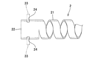
- a pair of slits 24 and 24 into which the inner side portions of the sandwiching pieces 33 and 33 of the electrode plate 3 are inserted are formed on the peripheral surface of the conductive connection portion 22 according to this modification.
- the conductive connecting portion 22 is slid downward along the inner side portions of the holding pieces 33 and 33 in a state where the inner side portions of the holding pieces 33 and 33 and the slits 24 and 24 are engaged.
- FIG. 7 and 8 are a front view and a side view showing a modified example of the coiled electronic component 1.
- the coiled electronic component 1 includes a connecting member 6 made of a non-conductive member made of a plastic material or a ceramic material.
- the connecting member 6 connects the left and right electrode plates 3 and 3 to each other, for example, by bonding the upper surface of the joint portion 31 of the electrode plate 3 to the lower surfaces of both end portions.
- the conductive connection portions 22 provided at both ends of the electronic component body 2 are respectively inserted between the sandwiching pieces 33 and 33 of the electrode plates 3 and 3 that are phase-connected by the connecting member 6.
- the electronic component main body 2, the electrode plates 3 and 3, and the connecting member 6 are integrated by holding the conductive connection portion 22 of the electronic component main body 2 between the protrusion 34 and the concave portion 35 of the electrode plate 3.
- a chip-type electronic component is obtained.
- the electrode plates 3 and 3 are placed on the assembly target 5, and the assembly portion composed of the pair of electrode pads 51 and 51 provided on the assembly target 5 is joined to the electrode plates 3 and 3.
- FIG. 9 and 10 are a plan view and a front sectional view showing a second embodiment of the coiled electronic component 1
- FIG. 11 is a side sectional view showing a state in which the coiled electronic component 1 is assembled to the assembly target 5. is there.
- the coiled electronic component 1 according to the second embodiment includes a coil portion 21 having a spiral structure formed of a conductive material and conductive connections provided at both ends of the coil portion 21.
- the electronic component main body 2 including the portion 22 is provided.
- circular openings 25 that are externally fitted to positioning and fixing portions 52 made of ball-shaped solder material provided on the assembly target 5 are respectively formed in the conductive connection portions 22 and 22 of the electronic component body 2.
- the coiled electronic component 1 according to the second embodiment is different from the first embodiment.
- the electronic component main body 2 is set in a state where the opening 25 is externally fitted to the positioning fixing portion 52.
- the positioning fixing portion 52 is heated to a predetermined temperature to melt the ball-shaped solder material, so that the opening 25 of the conductive connection portion 22 is positioned at the assembly position of the assembly target 5 as shown in FIG. Soldered in the combined state.
- the coil portion 21 having a spiral structure formed of a conductive material as described above and the conductive connection portions 22 and 22 provided at both ends thereof are provided on the assembly target 5.
- the opening 25 of the conductive connection portion 22 is soldered to the positioning and fixing portion 52 of the assembly target 5 or the like.
- FIG. 12 is a side sectional view showing a first modification of the coiled electronic component 1 according to the second embodiment
- FIG. 13 is a side sectional view showing a second modification of the coiled electronic component 1 according to the second embodiment.
- FIG. 14 and FIG. 14 are partially enlarged views showing modifications of the electronic component main body 2.
- the assembly target 5 to which the coiled electronic component 1 according to the first modification is assembled is formed of a conductive material and has a protrusion 53 having a large-diameter spherical portion 54 on the upper part.
- a positioning and fixing portion is provided.
- the conductive connection portion 22 of the electronic component body 2 is formed with an opening 25 on the lower surface that is slightly smaller in diameter than the spherical portion 54 and slightly smaller in diameter than the body portion of the protrusion 53.
- the opening 25 of the conductive connection portion 22 is externally fitted to the protrusion 53 of the assembly target 5 and press-fitted below the spherical portion 54, whereby the opening 25 and the assembly target 5 of the conductive connection portion 22 are pressed.
- a connection state in which the inner peripheral surface of the opening 25 is press-contacted with the outer peripheral surface of the protrusion 53 is obtained in a state where the assembly position is aligned.
- the coiled electronic component 1 according to the second modification has the first and second openings 25 and 26 formed in the conductive connection portion 22 of the electronic component body 2 as shown in FIG. It is different from one modification.
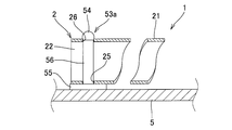
- a spherical portion 54 having a larger diameter than the upper opening 26 is formed above the protrusion 53a made of a conductive material provided on the assembly target 5, and below the protrusion 53a, a lower portion is formed.
- a flange 55 having a diameter larger than that of the opening 25 is formed.
- a columnar body portion 56 having a smaller diameter than the openings 25 and 26 and a length corresponding to the outer diameter of the conductive connection portion 22.
- the openings 25 and 26 of the conductive connection portion 22 are externally fitted to the protrusions 53a of the assembly target 5, and are press-fitted below the spherical portion 54, whereby the inner peripheral surfaces of both openings 25 and 26 are obtained.
- a connection state is obtained in which the lower surface of the conductive connection portion 22 is in pressure contact with the upper surface of the flange portion 55.
- the opening portion 25 of the conductive connection portion 22 and the assembly target are visually observed. It is possible to easily determine whether or not the connection with the five protrusions 53a has been successfully made.
- the one slit 23 extended spirally toward the other end part from the one end part of the cylindrical body which consists of a raw material which has electroconductivity is formed along the surrounding surface of the said cylindrical body.
- the example in which the coil portion 21 of the electronic component main body 2 is formed has been described.
- the spiral is formed from the conductive connection portion 22 provided on one end portion side of the electronic component main body 2 toward the other end portion side. It is good also as a structure which provided the pair of coil parts 21a and 21b extended in parallel with a fixed space
- a coiled electronic component includes an electronic component main body having a spiral coil portion formed of a conductive material, and conductive connection portions provided at both ends thereof, and the conductive connection portion.
- An opening is provided so as to receive the insertion of the conductive connection portion therebetween.
- the pair of sandwiching pieces have a configuration in which a protrusion projecting inwardly into the opening is provided at a site upstream in the insertion direction of the conductive connection portion.
- the conductive connection portion of the electronic component main body is pressed against the protrusion from the upstream side in the insertion direction to elastically deform both sandwiching pieces, thereby the conductive connection portion on the downstream side in the insertion direction of the protrusion. Can be inserted smoothly.
- the conductive connection portion is fitted on the downstream side of the protrusion and the conductive connection portion is sandwiched between the two sandwiching pieces, the movement of the conductive connection portion is regulated by the protrusions of the sandwiching piece, and the dropping is prevented. There is an advantage that it can be effectively prevented.
- the conductive connection portion may be formed with a slit into which the inner side portions of the pair of sandwiching pieces are inserted.
- the conductive connection portion can be smoothly moved to the holding position by slidingly moving the conductive connection portion along the pair of holding pieces in a state where the inner side portion of the holding piece and the slit are engaged. It is possible to move. And, by sandwiching the conductive connection portion of the electronic component body between both sandwiching pieces, the connection state between the conductive connection portion and the electrode can be stably maintained, and the electronic component body can be removed from the electrode. There is an advantage that it can be surely prevented.
- it may be configured to include a connecting member made of a non-conductive member that connects the pair of electrodes to each other.
- the chip-type electronic component in which the electronic component main body, the electrode, and the connecting member are integrated by inserting and holding the conductive connection portion of the electronic component main body between the electrode clamping pieces. It is possible to form the electronic component, and it is possible to easily perform an operation of mounting and mounting the electronic component on an assembly target.
- a coiled electronic component includes a spiral coil portion formed of a conductive material, and conductive connection portions provided at both ends of the coil portion. An opening corresponding to the positioning and fixing portion provided on the assembly target is formed.
- FIG. 15 is a perspective view schematically showing a configuration of coil component 1A according to one aspect of the present invention.
- FIG. 16 is a plan view showing a state in which the coil component 1A is disassembled into components
- FIG. 17 is a plan sectional view showing a specific structure of the coil component 1A
- FIG. 18 shows a specific structure of the coil component 1A.
- 15 is a cross-sectional view taken along line IV-IV in FIG. 15, FIG.
- FIG. 19 is a front cross-sectional view showing a state where the coil component 1A is mounted on the assembly target 5A
- FIG. 20 is a modified example of the electronic component body 2A constituting the coil component 1A
- FIG. 21 is a plan sectional view showing a state of the magnetic flux J generated when the coil component 1A is energized.
- the coil component 1A includes an electronic component main body 2A made of a nickel or nickel alloy conductive material, a housing case 3A made of a non-conductive material for housing the electronic component main body 2A, and both ends of the electronic component main body 2A. A pair of electrodes 4A and 4A to be connected is provided.
- the coil component 1A is a chip-type electronic component having a so-called chip component shape.
- the electronic component body 2A is formed of a cylindrical body having a diameter of about 50 ⁇ m to 500 ⁇ m.
- a coil portion 21A having a spiral structure is formed in the central portion of the electronic component main body 2A over a length of, for example, about 0.5 to 1.0 mm, and cylindrical electric connection portions 22A are formed at both ends thereof. Is provided.
- a slit 23A that spirally extends from one end portion to the other end portion is formed on the peripheral surface of the cylindrical body. Is formed along the slit 23A to form a predetermined region of the electronic component main body 2A with the spiral coil portion 21A.
- the coil portion 21A can be easily and appropriately formed on the extremely small electronic component body 2A.
- the mass production can be achieved.
- the coil portion 21A and the slit 23A are simultaneously formed by an electroforming method or a forming method using a three-dimensional metal printer. It may be.
- the cross-sectional shape of the electronic component main body 2A is not limited to a circle, and may be various shapes such as a square or a hexagon.
- a non-conductive material such as a ceramic material or a plastic material has a U-shaped cross section having a bottom wall portion 31A and a pair of left and right side wall portions 32A, 32A, and the upper surface and both end surfaces thereof are respectively
- the opened storage case 3A is formed.
- the total length L3 of the housing case 3A is formed to be shorter than the total length L2 of the electronic component main body 2A.
- the installation interval W3 between the side wall portions 32A and 32A is set to a value larger than the diameter D2 of the electronic component main body 2A, so that the electronic component main body 2A can be accommodated in the accommodating case 3A ( (See FIG. 16).
- the electrode 4A has an end plate 41A that covers an opening formed on the end surface of the housing case 3A, and a peripheral wall 42A that is fitted around the end of the housing case 3A. Further, the electrode 4A is formed with a through hole 43A made of a round hole or the like for allowing the magnetic flux J (see FIG. 21) generated when the electronic component main body 2A is energized to pass through substantially the center of the end plate 41A. Furthermore, the installation interval of both electrodes 4A, 4A, specifically, the installation interval of the inner wall surface of the end plate 41A is set equal to the total length L3 of the housing case 3A, thereby being shorter than the total length L2 of the electronic component main body 2A. Is set to a value.
- the electrode 4A including the end plate 41A and the peripheral wall 42A is formed by, for example, bending a plate material made of a conductive material such as copper, nickel, or silver. Then, in the step of disposing the electrode 4A, the peripheral wall 42A of the electrode 4A is externally fitted to the end portion of the housing case 3A, so that the end surface of the housing case 3A is covered with the end plate 41A of the electrode 4A.
- the electrode 4A can also be formed by applying a conductive paste obtained by adding glass frit to a metal powder to the end of the housing case 3A and then heating and baking it at a predetermined temperature. According to this method, it is possible to simultaneously form the electrode 4A and dispose the electrode 4A.
- the installation interval (L3) between the electrodes 4A and 4A is set to be shorter than the total length L2 of the electronic component main body 2A. For this reason, if the electronic component main body 2A is compressed and deformed and accommodated in the accommodating case 3A, as shown in FIG. 17, the electrical connection portion 22A is connected to the electrode 4A according to the restoring force of the electronic component main body 2A. The two end portions of the electronic component main body 2A are electrically connected to both the electrodes 4A by being pressed against the end plate 41A.
- the electrode 4A is disposed at both ends of the housing case 3A in the disposing step of the electrode 4A.
- the electrical connection portions 22A provided at both ends of the electronic component body 2A It can be electrically connected respectively is pressed against the face to the end plate 41A of the electrode 4A.
- the electrodes 4A and 4A disposed at both ends of the housing case 3A are replaced with a printed wiring board, a flexible board, a ceramic multilayer wiring board, an electrode plate for a liquid crystal display or a plasma display, a semiconductor substrate.
- Is mounted on the assembly target 5A, and the pair of electrode pads 51A, 51A provided on the assembly target 5A and the bottom surfaces of the electrodes 4A, 4A are connected by the solder 52 or the like to form a spiral structure.
- the coil component 1A having the electronic component body 2A in which the coil portion 21A is formed can be used as an inductance element, a T-type filter, an oscillation circuit, or the like.
- the electronic component main body 2A having the spiral coil portion 21A formed of a conductive material and the nonconductive material that accommodates the electronic component main body 2A are used.
- the cylindrical electrical connection portions 22A provided at both ends thereof are disposed at both ends of the housing case 3A.
- the electrodes 4A are configured to contact each other and connect.
- a plurality of thin ceramic plates each having a circular conductor portion are laminated, and formed on both ends of a chip coil body made of a laminate of the ceramic plates.
- the coil component 1A is less likely to cause poor contact between the conductor portions, and the coil component 1A is formed very easily. can do.
- the electronic component body 2A can be accommodated in the housing case 3A and protected, the damage can be prevented even in the extremely small coil component 1A in which the entire length and diameter of the electronic component body 2A are set to be extremely small.
- the coil component 1A can be easily and properly mounted on the assembly target 5A made of a substrate or the like.
- the slit 23A extends spirally from one end portion to the other end portion of the cylindrical body. Since the coil part 21A having a spiral structure is formed on the electronic component main body 2A by forming along the circumferential surface of the cylindrical body, by an etching method, a modeling processing method using a laser processing machine, or the like, The following extremely small electronic component main body 2A can be easily and appropriately molded and mass-produced.
- an inductance element having an inductance of about 100 pH can be easily and appropriately formed.
- the electronic component main body 2A is accommodated in the housing case.
- These electrical connections can be made easily and appropriately by accommodating the both ends of the electronic component main body 2A in contact with the electrode 4A.
- the installation interval (L3) between the electrodes 4A and 4A disposed at both ends of the housing case 3A is set shorter than the total length L2 of the electronic component body 2A
- the electronic component body 2A By simply compressing and deforming and accommodating in the housing case 3A, the both end portions are pressed against the end plate 41A of the electrode 4A according to the restoring force of the electronic component main body 2A. There is an advantage that an electrical connection state can be obtained.
- the housing case 3A is replaced in the connecting step between the electronic component main body 2A and the electrode 4A in place of the configuration in which both end portions are pressed against the end plate 41A of the electrode 4A or in accordance with the restoring force of the electronic component main body 2A.
- the both ends of the electronic component main body 2A are connected to the electrodes 4A and 4A, respectively, by soldering the end of the electronic component main body 2A accommodated in the electrode 4A to the electrode 4A or by adhering it with a conductive adhesive. Also good.
- the cylindrical electrical connection portions 22A provided at both ends of the electronic component main body 2A may be omitted, and the spiral coil portion 21A may be formed over the entire length of the electronic component main body 2A.
- the end portion of the coil portion 21A is pressed against the end plate 41A of the electrode 4A according to the restoring force of the electronic component main body 2A, or the end portion of the coil portion 21A and the electrode 4A are soldered.
- the end of the electronic component main body 2A can be electrically connected to the electrode 4A.
- the electronic component main body 2A is formed by forming a single slit 23A spirally extending from one end portion to the other end portion of the cylindrical body made of a conductive material along the peripheral surface of the cylindrical body.
- the example of forming the coil portion 21A has been described, but as shown in FIG. 20, a pair of spirally extending from the electrical connection portion 22A provided on one end side of the electronic component main body 2A toward the other end portion side.
- a pair of coil portions 21Aa and 21Ab extending in parallel at regular intervals may be provided in the electronic component main body 2A.
- the coil component 1A has a structure in which the through hole 43A for passing the magnetic flux generated when the electronic component main body 2A is energized is provided in the end plate 41A of the electrode 4A, the coil component 1A is used as an inductance element or the like.
- the flow of the magnetic flux J generated when the electronic component main body 2A is energized can be prevented from being obstructed by the electrode 4A, and the performance of the coil component 1A can be exhibited well. it can.
- both ends of the electronic component body 2A can be brought into contact with the electrode 4A and the magnetic flux J As long as the shape and position can pass through, it is possible to form through holes of various shapes such as square holes at arbitrary positions on the electrode 4A.
- the housing case 3A is not limited to a U-shaped cross section having a bottom wall portion 31A and a pair of left and right side wall portions 32A, 32A, but a cylindrical body having a circular cross section made of a nonconductive material such as a ceramic material or a plastic material, Alternatively, the housing case may be formed of a square cylinder having a square cross section, and the electronic component main body 2A may be inserted from one end thereof, and then the electrodes 4A may be disposed at both ends of the housing case.
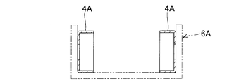
- FIGS. 23A and 23B are process diagrams showing a forming process of the housing case 34A according to this another embodiment.
- the housing case 34A In order to mold the housing case 34A, first, as shown in FIG. 23A, after the pair of electrodes 4A and 4A are set on the jig 6A at an interval corresponding to the entire length of the electronic component main body 2A, as shown in FIG. 23B, An electronic component body 2A is disposed between the electrodes 4A and 4A. Next, a filler made of a non-conductive material such as a silicon resin material is filled between the electrodes 4A and 4A so as to surround the outer peripheral portion of the electronic component main body 2A, and is cured. Thereby, as shown in FIG. 22, the housing case 34A composed of a covering layer surrounding the electronic component body 2A is formed, and the electrodes 4A and 4A are disposed so as to cover both ends thereof. 2A and electrodes 4A and 4A are joined.
- a filler made of a non-conductive material such as a silicon resin material
- a curable expansive material such as a curable expansive resin or gypsum having a property of expanding at the time of curing
- the storage case 34A is formed using the filler made of the curable and expansive material
- the electronic component main body 2A is expanded since the electronic component main body 2A is integrally held when the filler is cured.
- the housing case 34A when a heat-resistant material is used as the filler constituting the housing case 34A, even if the coil component 1A is used in a high temperature environment of, for example, 200 ° C. or higher, the electronic component main body 2A is thermally deteriorated. Can be effectively suppressed by the housing case 34A made of a heat-resistant material.
- FIG. 24 is an explanatory view showing a modified example of the connecting step of connecting both ends of the electronic component main body 2A to the electrode 4A.
- a welding current of about 1 ampere is applied to the electrodes 4A and 4A and the electronic component main body 2A disposed between the energizing device 7A having the power source 71A, the open / close switch 72A and the ammeter 73A.
- the joints between the electrodes 4A and 4A and the electronic component main body 2A are heated and welded.
- the both ends of the electronic component main body 2A are welded to the electrode 4A simply by supplying a welding current from the energizing device 7A to the electrodes 4A and 4A and the electronic component main body 2A disposed therebetween.
- a welding current from the energizing device 7A to the electrodes 4A and 4A and the electronic component main body 2A disposed therebetween.
- there is an advantage that whether or not the electrodes 4A, 4A and the electronic component main body 2A are properly welded can be inspected at the same time according to the measurement value of the ammeter 73A.
- the coil component according to one aspect of the present invention includes an electronic component main body having a spiral coil portion formed of a conductive material, and a housing case made of a non-conductive material that houses the electronic component main body, A pair of electrodes connected to both ends of the electronic component body, and the pair of electrodes are respectively disposed at both ends of the housing case.
- the electronic component main body having the coil portion of the spiral structure is accommodated in the accommodating case, so that the end portions of the electronic component main body are brought into contact with the electrodes disposed at both ends of the accommodating case. While being able to connect, the electronic component main body can be protected by the housing case. For this reason, even in a very small coil component in which the overall length and diameter of the electronic component main body are set to be extremely small, damage to the electronic component main body can be effectively prevented, and problems such as poor contact can be suppressed while the coil is suppressed. There exists an advantage that the manufacturing cost of components can be held down cheaply.
- the storage case may have an end plate in which both ends of the storage case are opened, and the electrodes are arranged so as to cover the opening of the storage case.
- the electronic component main body is accommodated in the housing case, and both the end portions of the electronic component main body are brought into contact with the end plates of the electrodes, respectively, so that the electrical connection can be easily and appropriately performed.
- the installation interval of the pair of electrodes is set to be shorter than the total length of the electronic component main body.
- each electrode has a through hole for allowing a magnetic flux generated when the electronic component body is energized to pass therethrough.
- the electronic component main body when used as an inductance element or the like, it is possible to prevent the magnetic flux generated when the electronic component main body is energized from being obstructed by the electrode.
- the performance of the main body can be exhibited well.
- a method of manufacturing a coil component according to one aspect of the present invention includes: (a) a molding step of the electronic component body that molds an electronic component body having a spiral coil portion formed of a conductive material; and (b). A forming step of the storage case for forming a storage case made of a non-conductive material for storing the electronic component main body; and (c) an electrode disposing step of disposing electrodes at both ends of the electronic component main body, respectively. (D) A step of connecting the electronic component main body and the electrode, wherein both ends of the electronic component main body are brought into contact with and connected to the electrodes, respectively.
- the electronic component main body is housed in the housing case in the connecting step (d). Both ends of the component main body are pressed and electrically connected to the electrodes, respectively, and the coil component in which the electronic component main body is protected by the housing case can be easily and appropriately manufactured.
- the spirally extending from one end portion to the other end portion of the cylindrical body along the peripheral surface of the cylindrical body made of a conductive material It is desirable to form the coil part of the electronic component body by forming a slit.
- the coil portion can be easily and appropriately formed on an extremely small electronic component main body by an etching method or a modeling method using a laser processing machine, so that mass production thereof is achieved. Can do.
- a non-conductive material is formed on the outer peripheral portion of the electronic component main body.
- a housing case surrounding the electronic component main body may be formed by filling and curing the filler.
- the electronic component main body can be held in a state where the electronic component main body is integrally held when the filler is cured, so that the electronic component main body can be stably held in the housing case. Can do.
- non-conductive material is preferably a curable and expandable material.
- the electronic component main body expands in a state of integrally holding the electronic component main body. There is an advantage that the state can be obtained.
- a current for welding is applied to the electronic component main body from between the electrodes so as to weld both ends of the electronic component main body to the electrode, respectively. It may be.
- both ends of the electronic component main body can be connected to the electrodes by simply passing a welding current through the electronic component main body and the electrodes disposed at both ends thereof, and the welding is performed.
- a welding current By measuring the current value for use, there is an advantage that it can be easily inspected whether or not the welding between the electrode and the electronic component main body is properly performed.
- the coil component having such a configuration and the manufacturing method thereof, it is possible to suppress the occurrence of contact failure in the electronic component and to suppress the manufacturing cost thereof at a low cost.
- inductance element a T-type filter, an oscillation circuit, and a method for manufacturing the inductance element will be described.
- the present invention relates to an inductance element having a plurality of coils, a T-type filter using the inductance element, an oscillation circuit, and a method for manufacturing the inductance element.
- circuits that require a coil have been widely used in various electronic circuits such as wireless communication devices.
- the frequencies handled by the oscillation circuit, the tuning circuit, the matching circuit, and the like are affected by the resonance frequency f of the LC circuit.
- the frequency handled by a circuit has increased, and a circuit having a high resonance frequency f is required. In order to increase the resonance frequency f, it is necessary to reduce the inductance L.
- each ring-shaped pattern does not conduct.
- the chip coil created by such a manufacturing method needs to be stacked by the number of turns of the coil, and the contact connection portion between the through hole and the ring-shaped pattern is generated. Inconvenient contact failure is likely to occur. Further, although this chip coil becomes a single coil, there is a need to increase the number of components that can be integrated into one component.
- An object of the present invention is to provide an inductance element that can easily reduce the possibility of occurrence of defects and improve the degree of integration of coils, a T-type filter using the inductance element, an oscillation circuit, and the inductance element It is to provide a manufacturing method.
- An inductance element connects a plurality of coils and makes them electrically connected to each other at a coil portion in which a plurality of coils are arranged so as to form a multiple helix separated from each other and one end of the multiple helix.
- a conduction connecting portion connects a plurality of coils and makes them electrically connected to each other at a coil portion in which a plurality of coils are arranged so as to form a multiple helix separated from each other and one end of the multiple helix.
- the inductance element having such a configuration can support a plurality of coils arranged so as to form a multiple helix apart from each other by a conductive connecting portion.
- a multiple helix can be manufactured without stacking a plurality of ceramic plates on which ring-shaped copper wiring patterns are formed as in the manufacturing method described in the background art. Therefore, there is no possibility of contact failure between the layers, and it is easy to reduce the risk of failure.
- the plurality of coils are arranged so as to form a multiple helix separated from each other, the plurality of coils can be integrated in a single element. Therefore, the inductance element having such a configuration can easily improve the degree of integration of the coil.
- the conduction connecting portion has a cylindrical shape concentric with the multiple helix.
- the inductance element having such a shape can be formed by processing a cylindrical body having a cylindrical shape, manufacture is facilitated.
- the multiple helix preferably has a shape in which the coils are separated by a spiral slit along a circumferential surface of a cylindrical body obtained by extending the conductive connecting portion in the axial direction.
- the inductance element can be formed by forming the plurality of spiral slits along the peripheral surface of the cylindrical body, the plurality of coils can be easily formed integrally. .
- the transformer is a transformer in which one of the plurality of coils is a primary coil and at least one of the plurality of coils different from the primary coil is a secondary coil.
- this inductance element can function as a transformer.
- the length of the coil part is preferably 0.5 mm to 1 mm, and the diameter of the coil part is preferably 50 ⁇ m to 500 ⁇ m.
- the self-inductance of each coil can be set to about 30 to 100 pH.
- a coil having such a small value of self-inductance can be easily applied to a high-frequency circuit.
- a T-type filter includes the above-described inductance element and a capacitor, the number of the coils is two, and one terminal of the capacitor is connected to the conduction connecting portion.
- the two coils are connected in series, and one terminal of the capacitor is connected to the connection point of the two coils.
- the T-type filter can be configured by combining a single inductance element and a capacitor, it is easy to configure a T-type filter circuit.
- An oscillation circuit includes the above-described inductance element and a capacitor, wherein one terminal of the capacitor is connected to one of the plurality of coils, and the other terminal of the capacitor is the one terminal.
- the coil is connected to a position that is a predetermined distance away from the connection point of the one terminal or to the conduction connecting portion.
- the oscillation circuit can be configured by combining a single inductance element and a capacitor, it is easy to configure the oscillation circuit.
- An inductance element manufacturing method is the above-described inductance element manufacturing method, wherein one end portion of the cylindrical body is disposed along the peripheral surface of the conductive cylindrical body, By forming a plurality of spiral slits spaced apart from each other in a region between the other end of the cylindrical body and a predetermined position spaced apart by a predetermined length in the direction of the one end, the spiral region is formed in the region between A plurality of coils are formed as the coil portion, and a region from the other end portion to the predetermined position is defined as the conduction connecting portion.
- a plurality of coils are formed on a conductive cylindrical body by forming a plurality of spiral slits along the peripheral surface thereof to form a coil portion, and a slit is formed. Since the unconnected region can be used as the conductive connection portion, it is easy to form the above-described inductance element. Further, according to this manufacturing method, the entire inductance element can be manufactured as an integral part. Therefore, unlike the manufacturing method described in the background art, there is no need to stack a plurality of ceramic plates on which a ring-shaped copper wiring pattern is formed, so that there is no possibility of poor contact between the stacks. Therefore, according to this manufacturing method, it is easy to reduce the possibility that the inductance element is defective.
- the slits by etching or laser processing.
- Etching or laser processing is suitable as a processing means for forming a spiral slit in a cylindrical body.
- the inductance element having such a configuration, the T-type filter using the inductance element, and the oscillation circuit can easily reduce the risk of occurrence of defects and improve the degree of integration of the coils. Moreover, such a manufacturing method is suitable for manufacturing this inductance element. (Fourth embodiment)
- FIG. 25 is a front view showing an appearance of the inductance element according to the embodiment of the present invention.
- the inductance element 1B shown in FIG. 25 connects the coils 2B and 3B at one end of the multiple helix and a coil portion 11B arranged so that a plurality of coils 2B and 3B are separated from each other. It is configured to include a multi-spiral and a concentric cylindrical part 12B (conducting connection part) to be conducted.
- the inductance element 1B shows an example in which the number of coils has a double spiral structure with two coils.
- the inductance element 1B includes two coils 2B and 3B, and the coil portion 11B has a double helix. However, there may be three or more coils, and the coil portion 11B. May have a triple or more multi-helical structure. Moreover, although the example in which the length and the number of turns of the coil 2B and the coil 3B are equal is shown, the length and the number of turns of each coil may be different from each other.
- FIG. 26 is a circuit diagram showing an electrical configuration of the inductance element 1B shown in FIG.
- the end of the coil 2B serves as one terminal 21B of the coil 2B
- the end of the coil 3B serves as one terminal 31B of the coil 3B
- the cylindrical portion 12B serves as a common terminal for the coils 2B and 3B. Since the coil 2B and the coil 3B are coaxially wound so as to be combined with each other to form a double helix, a magnetic flux penetrates the coil 2B and the coil 3B, thereby generating a mutual inductance.
- the inductance element 1B constitutes a transformer having one of the coils 2B and 3B as a primary coil and the other as a secondary coil. Further, since the inductance element 1B can integrate the two coils 2B and 3B with a single element, it is easy to improve the degree of integration of the coils. Further, the inductance element 1B can form a transformer with a single element.
- the length A of the coil part 11B is preferably 0.5 mm to 1 mm, and the diameter D of the coil part 11B is preferably 50 ⁇ m to 500 ⁇ m.
- the length A of the coil portion 11B is 1 mm, the number of turns of each of the coils 2B and 3B is 5 times, and the diameter D of the coil portion 11B is 130 ⁇ m, the self-inductance of the coils 2B and 3B is 44 pH.
- the resonance frequency f is 24 GHz. If the number of turns of the coils 2B and 3B is set to 3 and the diameter D is adjusted, the resonance frequency f can be set to 70 GHz in combination with a 1 pF capacitor.
- a method for manufacturing the inductance element 1B will be described.
- a cylindrical body having conductivity such as nickel or a nickel alloy is prepared.
- the peripheral surface of the cylindrical body from one end of the cylindrical body (right end in the example of FIG. 25) and the other end of the cylindrical body (left end in the example of FIG. 25)
- a plurality of spiral slits spaced apart from each other in a region between the predetermined position B separated by a predetermined length in the direction of one end, a plurality of spiral coils 2B and 3B are formed in that region.
- a cylindrical portion 12B is formed in a region from the other end portion to a predetermined position B as a portion 11B.
- Etching or laser processing can be suitably used as the slit formation method.
- the present invention is not limited to an example in which a plurality of coils are formed by forming slits in a conductive cylindrical body, and the inductance element 1B may be formed by using, for example, electroforming or a three-dimensional printer.
- the cylindrical-shaped cylindrical part 12B was shown as an example of a conduction
- the inductance element 1B shown in FIG. 25 can be manufactured as an integral part by using the above-described manufacturing method. Therefore, there is no need to stack a plurality of ceramic plates on which ring-shaped copper wiring patterns are formed as in the manufacturing method described in the background art, and contact the wiring patterns of each layer, which may cause poor contact between the stacks. There is no. Therefore, according to the inductance element 1B and the manufacturing method thereof shown in FIG. 25, it is easy to reduce the possibility that the inductance element 1B is defective. (Fifth embodiment)
- FIG. 27 is a front view showing an example of the configuration of the T-type filter according to the fifth embodiment of the present invention.
- a T-type filter 5B shown in FIG. 27 includes an inductance element 1B and a capacitor 4B.
- the capacitor 4B includes a substantially rectangular parallelepiped chip body 41B and electrodes 42B and 43B formed on both ends of the chip body 41B.
- the electrode 42B of the capacitor 4B and the cylindrical portion 12B are connected by the connecting portion 6B.
- connection means between the cylindrical part 12B and the electrode 42B by the connection part 6B various connection means such as electric welding, brazing with silver wax, adhesion with a conductive adhesive, and soldering can be used.
- the cylindrical portion 12B and the electrode 42B are not limited to an example of being directly connected, and may be connected by a connection portion 6B including a connection member such as a printed wiring board or a metal fitting.
- FIG. 28 is a circuit diagram showing an example of the electrical configuration of the T-type filter 5B shown in FIG.
- the coils 2B and 3B are connected in series, and the electrode 42B of the capacitor 4B is connected to the cylindrical portion 12B that is the connection point of the coils 2B and 3B.
- a T-type filter is obtained in which the electrode 43B of the capacitor 4B constitutes the filter terminal.
- the T-type filter 5B can be configured by combining the single inductance element 1B and the capacitor 4B, it is easy to configure the T-type filter circuit. (Sixth embodiment)
- FIG. 29 is a front view showing an example of the configuration of the oscillation circuit according to the sixth embodiment of the present invention.
- An oscillation circuit 7B shown in FIG. 29 includes an inductance element 1B and a capacitor 4B.
- An inductance element 1B shown in FIG. 29 shows an example in which the number of turns and the length of the coil 3B are shorter than those of the coil 2B.
- the electrode 42B of the capacitor 4B and the cylindrical portion 12B are connected by the connecting portion 6B, and the electrode 43B of the capacitor 4B and the terminal 31B of the coil 3B are connected by the connecting portion 8B.
- connection unit 8B the same connection means as the connection unit 6B can be used.
- An oscillation circuit 7B shown in FIG. 29 shows an example in which the connection portions 6B and 8B connect the capacitor 4B and the inductance element 1B via a connection member such as a printed wiring board or a metal fitting.
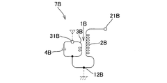
- FIG. 30 is a circuit diagram showing an example of the electrical configuration of the oscillation circuit 7B shown in FIG.
- the coil 3B and the capacitor 4B are connected in parallel to constitute an LC resonance circuit, and the coil 3B and the coil 2B constitute a transformer.
- an oscillation circuit is configured.
- the wireless tuning circuit can be configured by connecting the cylindrical portion 12B to the circuit ground and connecting the terminal 31B to the antenna.
- the electrode 43B is not necessarily limited to the example connected to the terminal 31B of the coil 3B, and may be connected to an intermediate position of the coil 3B. Further, the electrode 42B is not necessarily limited to the example of being connected to the cylindrical portion 12B, and may be connected to the position of the coil 3B that is separated from the connection portion between the electrode 43B and the coil 3B by a predetermined distance according to a desired inductance. Good.
Landscapes
- Engineering & Computer Science (AREA)
- Power Engineering (AREA)
- Manufacturing & Machinery (AREA)
- Microelectronics & Electronic Packaging (AREA)
- Computer Networks & Wireless Communication (AREA)
- Signal Processing (AREA)
- Coils Or Transformers For Communication (AREA)
Abstract
コイル状電子部品は、導電性素材により形成された螺旋構造のコイル部と、その両端部に設けられた導電接続部とを有する電子部品本体と、前記導電接続部を組付対象に設けられた組付部にそれぞれ接続する一対の電極とを備え、当該電極が、前記導電接続部を挟持する一対の挟持片を有し、前記一対の挟持片は、互いの間に前記導電接続部の嵌入を受け入れるように開口している。
Description
本発明は、基板等からなる組付対象に組み付けられるコイル状電子部品、コイル部品、コイル部品の製造方法、インダクタンス素子、T型フィルタ、発振回路、及びインダクタンス素子の製造方法に関する。
近年、車載用の通信装置等に使用される電子部品は、その機能の向上とともに、ますます小型化が図られている。このような極小の電子部品を製造する方法として、リング状の銅配線パターンが形成された複数枚のセラミック板(ガラス層)を積層し、このセラミック板からなる積層体の両端に外部電極を形成し、この外部電極により各セラミック板の導体部同士を接続するようにした製造方法が知られている(例えば、特許文献1参照)。
しかしながら、上述の製造方法では、複数枚のセラミック板を極めて高精度に位置決めする必要がある。そのため、この位置決めがずれると各リング状パターンが導通しない導通不良が生じることが避けられない。また、このような製造方法で作成されたチップコイルは、コイルの巻数の数だけセラミック板を積層する必要があり、その数だけスルーホールとリング状パターンとの接続部が形成される。そのため、リング状パターン相互間で接触不良が生じ易かったり、製造コストが高価になったりする等の不都合があった。
本発明の目的は、電子部品に接触不良が発生するのを抑制し、かつその製造コストを安価に抑えることが容易なコイル状電子部品を提供することである。
本発明の一局面に従うコイル状電子部品は、導電性素材により形成された螺旋構造のコイル部と、その両端部に設けられた導電接続部とを有する電子部品本体と、前記導電接続部を組付対象に設けられた組付部にそれぞれ接続するための一対の電極とを備え、前記電極は、前記導電接続部を挟持する一対の挟持片を有し、前記一対の挟持片は、互いの間に前記導電接続部の嵌入を受け入れるように開口している。
また、本発明の一局面に従うコイル状電子部品は、導電性素材により形成された螺旋構造のコイル部と、当該コイル部の両端部に設けられた導電接続部とを備え、当該導電接続部に、組付対象に設けられた位置決め固定部に対応する開口部が形成されたものである。
本発明の一局面に従うコイル部品は、導電性を有する素材により形成された螺旋構造のコイル部を有する電子部品本体と、当該電子部品本体を収容する非導電性素材からなる収容ケースと、前記電子部品本体の両端部に接続される一対の電極とを備え、当該一対の電極が、前記収容ケースの両端部にそれぞれ配設されたものである。
本発明の一局面に従うコイル部品の製造方法は、(a)導電性を有する素材により形成された螺旋構造のコイル部を有する電子部品本体を成形する当該電子部品本体の成形工程と、(b)当該電子部品本体を収容する非導電性素材からなる収容ケースを成形する当該収容ケースの成形工程と、(c)前記電子部品本体の両端部にそれぞれ電極を配設する当該電極の配設工程と、(d)前記電子部品本体の両端部を前記電極にそれぞれ当接させて接続する前記電子部品本体と前記電極との接続工程とを備えたものである。
本発明の一局面に従うインダクタンス素子は、複数のコイルが互いに離間した多重螺旋を構成するように配置されたコイル部と、前記多重螺旋の一端部で、前記複数のコイルを連結すると共に互いに導通させる導通連結部とを備える。
また、本発明の一局面に従うT型フィルタは、上述のインダクタンス素子と、キャパシタとを備え、前記コイルの数は二つであり、前記キャパシタの一方端子が前記導通連結部に接続されていることによって前記二つのコイルが直列接続され、当該二つのコイルの接続点に前記キャパシタの一方端子が接続されている。
また、本発明の一局面に従う発振回路は、上述のインダクタンス素子と、キャパシタとを備え、前記キャパシタの一方端子が前記複数のコイルのうち一つに接続され、前記キャパシタの他方端子が前記一つのコイルにおける前記一方端子の接続箇所から所定距離離間した位置又は前記導通連結部に接続されている。
また、本発明の一局面に従うインダクタンス素子の製造方法は、上述のインダクタンス素子の製造方法であって、導電性の筒状体の周面に沿うように、前記筒状体の一端部と、前記筒状体の他端部から前記一端部方向へ所定長さ離間した所定位置との間の領域に互いに離間した螺旋状の複数のスリットを形成することによって、前記間の領域に前記螺旋状の複数のコイルを形成して前記コイル部とし、前記他端部から前記所定位置までの領域を前記導通連結部とする。
以下、本発明の一局面に従うコイル状電子部品1の実施形態を図面に基づいて説明する。なお、各図において同一の符号を付したものは、同一の構成であることを示し、その具体的な説明を省略する。
(第一実施形態)
(第一実施形態)
図1は、本発明の第一実施形態に係るコイル状電子部品1を示す斜視図、図2は、コイル状電子部品1を構成する電子部品本体2と電極板3,3(電極)とを分解した状態を示す正面図、図3は、コイル状電子部品1の具体的構造を示す側面図、図4は、基板等からなる組付対象5にコイル状電子部品1を組み付けた状態を示す正面図である。
コイル状電子部品1は、ニッケルあるいはニッケル合金の導電性を有する素材からなる電子部品本体2と、この電子部品本体2の両端部を、組付対象に設けられた電極パッド51,51からなる組付部に接続する一対の電極板3,3とを備えている。
電子部品本体2は、約50μm~500μmの直径(外径)を有する筒状体からなっている。電子部品本体2の中央部には、螺旋構造のコイル部21が例えば約0.5~1.0mmの長さに亘って形成されるとともに、その両端部には、円筒状の導電接続部22がそれぞれ設けられている。なお、電子部品本体2の内周面に、金メッキ等のメッキ層を設け、かつ電子部品本体2の外周部に、絶縁被覆層を設けた構造としてもよい。
電子部品本体2の成形方法としては、例えば導電性を有する素材からなる筒状体を形成した後、その一端部から他端部に向けて螺旋状に延びるスリット23を、前記筒状体の周面に沿って形成することにより、このスリット23を介して区画された螺旋構造のコイル部21を電子部品本体2の所定領域に形成する方法等が採用される。
また、スリット23の成形方法として、エッチング法、又はレーザ加工機を使用した造形加工法等を採用すれば、以下のような極小の電子部品本体2にコイル部21を容易かつ適正に成形して、その量産化を図ることができる。
例えば、電子部品本体2に設けられたコイル部21の全長を0.5mm~1.0mm、コイル部21の直径を50μm~500μmとし、コイル部の21の巻数を適宜に選定することにより、30pH~100pH程度のインダクタンスを有するインダクタンス素子を容易かつ適正に成形することができる。
なお、筒状体を形成した後にスリット23を形成するようにした前記実施形態に代え、電鋳法、または三次元金属プリンタを使用した成形法により、コイル部21とスリット23とを同時に成形するようにしてもよい。また、電子部品本体2の断面形状は、円形に限らず、正方形又は六角形等の種々の形状とすることができる。
電極板3は、組付対象5の組付部に設けられた電極パッド51に、はんだ付けされる等により接合される接合部31と、この接合部31の一端部から起立する起立部32とを有し、例えば銅、ニッケル又は銀等の導電性を有する素材からなるプレート材を折り曲げ加工される等により形成される。なお、電極の一例として板状の電極板3を示したが、電極は必ずしも板状、あるいは板状部材を加工したものに限らない。
起立部32は、電子部品本体2の導電接続部22を挟持する一対の挟持片33,33を有し、一対の挟持片33,33は、互いの間に導電接続部22の嵌入を受け入れるように開口しており、両挟持片33,33の間に電子部品本体2の導電接続部22が嵌入されて挟持されるように構成されている。具体的には、両挟持片33,33の内側面の離間距離が、電子部品本体2の外径と略同一か、この外径よりもやや小さい値に設定されている。これにより、両挟持片33,33の間に電子部品本体2の導電接続部22が嵌入された場合に、その周面に両挟持片33,33の内側面が圧接された状態で、電子部品本体2の導電接続部22が挟持されるようになっている。
また、挟持片33の上部、つまり導電接続部22の嵌入方向の上流側には、内向きに突出した三角形状の突部34が設けられている。この突部34の上面に電子部品本体2の導電接続部22を押し当てて、両挟持片33,33を弾性変形させることにより、突部34の下方(嵌入方向下流側)に導電接続部22をスムーズに嵌入し得るように構成されている。そして、導電接続部22の嵌入後には、挟持片33の突部34により導電接続部22の上方移動が規制されて、導電接続部22の脱落が防止されるようになっている。
さらに、電極板3の起立部32には、一対の傾斜面を有するV字型の凹部35が形成されている。そして、電子部品本体2の導電接続部22を突部34の下方に嵌入した際に、突部34の下面と凹部35の傾斜面とが導電接続部22の周面にそれぞれ圧接されるように、突部34と凹部35との間隔が設定されている。
上述の構成を有するコイル状電子部品1を、プリント配線基板、フレキシブル基板、セラミック多層配線基板、液晶ディスプレイやプラズマディスプレイ用の電極板、半導体基板等からなる組付対象5に組み付けるには、まず図4に示すように、電極板3,3を組付対象5の上に載置し、この組付対象5に設けられた一対の電極パッド51,51からなる組付部と電極板3,3の接合部31,31とをはんだ52等で接続する。
次いで、電極板3の起立部32に設けられた両挟持片33,33の間に、電子部品本体2の導電接続部22を嵌入して抱持させる。このようにして、螺旋構造のコイル部21を有する電子部品本体2が電極板3,3を介して組付対象5の電極パッド51,51に接続されることにより、インダクタンス素子、T型フィルタ又は発振回路等として使用されるコイル状電子部品1とすることができる。
本発明の一局面に従うコイル状電子部品1は、上述のように導電性素材により形成された螺旋構造のコイル部21と、その両端部に設けられた導電接続部22,22とを有する電子部品本体2と、この電子部品本体2の導電接続部22,22を、組付対象5に設けられた組付部にそれぞれ接続する一対の電極板3,3とを備え、この電極板3が、電子部品本体2の導電接続部22を挟持する一対の挟持片33,33を有し、前記一対の挟持片33,33が、互いの間に前記導電接続部22の嵌入を受け入れるように開口した構造を有している。その結果、コイル状電子部品1を極めて小型に形成した場合においても、コイル状電子部品1に接触不良が発生するのを抑制しつつ、その製造コストを安価に抑えることができるという利点がある。
すなわち、電子部品本体2の両端部に設けられた導電接続部22を、電極板3の挟持片33,33間に嵌入することにより、その内側面を前記円筒状の導電接続部22の周面にそれぞれ当接させて接続することができる。そのため、コイル状電子部品1は、特許文献1に示される従来技術のように、円形の導体部が形成された複数枚の薄いセラミック板を積層し、このセラミック板の積層体からなるチップコイル素体の両端に形成された外部電極により各セラミック板の導体部同士を接続する場合と比べて、導体部同士の接触不良が頻繁に生じる虞が少なく、かつ極めて簡単に前記コイル状電子部品1を形成することができる。
また、第一実施形態に示すように、挟持片33の上部に位置する導電接続部22の嵌入方向の上流側に、内向きに突出した三角形状の突部34を設けた構造とした場合には、この突部34の上面に電子部品本体2の導電接続部22を押し当てて、両挟持片33,33を弾性変形させることにより、突部34の下方に前記導電接続部22をスムーズに嵌入することができる。
しかも、導電接続部22を突部34の下方に嵌入して、導電接続部22を両挟持片33,33により挟持した状態では、この挟持片33の突部34により導電接続部22の上方移動を規制して、その脱落を効果的に防止できるという利点がある。なお、突部34の形状は、三角形に限られず、円弧状または台形状等の種々の形状に変更可能である。
さらに、第一実施形態に示すように、電極板3の起立部32に、一対の傾斜面を有するV字型の凹部35を形成し、この凹部35の傾斜面と突部34の下面とを導電接続部22の周面にそれぞれ圧接させるように、突部34と凹部35との間隔を設定した場合には、導電接続部22と電極板3とを、より確実に接続することができるという利点がある。
図5及び図6は、電子部品本体2の両端部に設けられた導電接続部22の変形例を示す正面図及び平面図である。
この変形例に係る導電接続部22の周面には、電極板3の挟持片33,33の内側辺部が挿入される一対のスリット24,24が形成されている。この構成によれば、挟持片33,33の内側辺部とスリット24,24とを係合した状態で、挟持片33,33の内側辺部に沿って導電接続部22を下方にスライド変位させることにより、その挟持位置へとスムーズに移動させることが可能である。
そして、挟持片33の内側辺部とスリット24とを係合することにより、導電接続部22と電極板3との接続状態を安定して保持することができる。しかも、電子部品本体2の前後方向(軸方向に沿う方向)の移動を挟持片33,33により規制することができるため、電極板3,3から電子部品本体2が脱落するのを確実に防止できるという利点がある。なお、スリット24,24に代えて、導電接続部22の周面を内方側に凹入させた凹部を設けることによっても同様の作用効果を得ることができる。
図7及び図8は、コイル状電子部品1の変形例を示す正面図及び側面図である。このコイル状電子部品1は、プラスチック材又はセラミックス材等からなる非導電性部材からなる連結部材6を備えている。この連結部材6は、両端部下面に電極板3の接合部31の上面が接着される等により、左右の電極板3,3を互いに連結するものである。
この構成によれば、連結部材6により相連結された両電極板3,3の挟持片33,33の間に、電子部品本体2の両端部に設けられた導電接続部22をそれぞれ嵌入して、電極板3の突部34と凹部35との間に電子部品本体2の導電接続部22を保持させることにより、電子部品本体2と、電極板3,3と、連結部材6とが一体化されたチップ型の電子部品が得られる。このため、電極板3,3を組付対象5の上に載置し、この組付対象5に設けられた一対の電極パッド51,51からなる組付部と、電極板3,3の接合部31,31とをはんだ52等で接続する作業を容易に行うことができる。
(第二実施形態)
(第二実施形態)
図9及び図10は、コイル状電子部品1の第二実施形態を示す平面図及び正面断面図、図11は、コイル状電子部品1を組付対象5に組み付けた状態を示す側面断面図である。
この第二実施形態に係るコイル状電子部品1は、第一実施形態と同様に、導電性素材により形成された螺旋構造のコイル部21と、このコイル部21の両端部に設けられた導電接続部22とからなる電子部品本体2を備えている。そして、組付対象5に設けられたボール状のはんだ材からなる位置決め固定部52に外嵌される円形の開口部25が、電子部品本体2の導電接続部22,22にそれぞれ形成されている点で、第二実施形態に係るコイル状電子部品1は、第一実施形態とは異なっている。
第二実施形態に係るコイル状電子部品1を組付対象5に組み付けるには、導電接続部22の開口部25と、組付対象5に設けられた位置決め固定部52とを位置合わせしつつ、電子部品本体2を組付対象5上に載置することにより、位置決め固定部52に開口部25を外嵌した状態で、電子部品本体2をセットする。次いで、位置決め固定部52を所定温度に加熱してボール状のはんだ材を溶融させることにより、図11に示すように、導電接続部22の開口部25が組付対象5の組付位置に位置合わせされた状態で、はんだ付けされるようになっている。
上述のように導電性素材により形成された螺旋構造のコイル部21と、その両端部に設けられた導電接続部22,22とを備え、この導電接続部22に、組付対象5に設けられた位置決め固定部52に対応する開口部25が形成されてなるコイル状電子部品1によれば、導電接続部22の開口部25を組付対象5の位置決め固定部52に、はんだ付けする等により容易に組み付けることができる。そのため、コイル状電子部品1を極めて小型に形成した場合においても、コイル状電子部品1に接触不良が発生するのを抑制しつつ、その製造コストを安価に抑えることができるという利点がある。
図12は、第二実施形態に係るコイル状電子部品1の第一変形例を示す側面断面図、図13は、第二実施形態に係るコイル状電子部品1の第二変形例を示す側面断面図、図14は、電子部品本体2の変形例を示す部分拡大図である。
第一変形例に係るコイル状電子部品1が組み付けられる組付対象5には、図12に示すように、導電性素材により形成されるとともに、上部に大径の球状部54を有する突起53からなる位置決め固定部が設けられている。また、電子部品本体2の導電接続部22には、球状部54よりもやや小径で、かつ突起53の本体部よりもやや小径の開口部25が、下面に形成されている。
上述構成において、導電接続部22の開口部25を組付対象5の突起53に外嵌して、球状部54の下方に圧入することにより、導電接続部22の開口部25と組付対象5の組付位置とを位置合わせした状態で、開口部25の内周面を突起53の外周面に圧接させた接続状態が得られることになる。
一方、第二変形例に係るコイル状電子部品1は、図13に示すように、電子部品本体2の導電接続部22に上下一対の開口部25,26が形成されている点で、前記第一変形例とは異なっている。そして、組付対象5に設けられた導電性素材からなる突起53aの上方には、上方の開口部26よりも大径の球状部54が形成されるとともに、突起53aの下方には、下方の開口部25よりも大径のフランジ部55が形成されている。また、球状部54とフランジ部55との間には、開口部25,26より小径で、かつ導電接続部22の外径に対応した長さを有する柱状の本体部56が設けられている。
上述の構成において、導電接続部22の開口部25,26を組付対象5の突起53aに外嵌して、球状部54の下方に圧入することにより、両開口部25,26の内周面を突起53の外周面にそれぞれ圧接させるとともに、導電接続部22の下面をフランジ部55の上面に圧接させた接続状態が得られる。また、コイル状電子部品1の組付状態では、大径の球状部54が導電接続部22の上方に突出するため、これを目視することにより、導電接続部22の開口部25と組付対象5の突起53aとの接続が良好に行われたか否かを容易に判別することができる。
なお、前記実施形態では、導電性を有する素材からなる筒状体の一端部から他端部に向けて螺旋状に延びる一本のスリット23を前記筒状体の周面に沿って形成することにより電子部品本体2のコイル部21を形成した例について説明したが、図14に示すように、電子部品本体2の一端部側に設けられた導電接続部22から他端部側に向けて螺旋状に延びる一対のスリット23a,23bを筒状体の周面に沿って形成することにより、一定間隔で平行に延びる一対のコイル部21a,21bを電子部品本体2に設けた構造としてもよい。
すなわち、本発明の一局面に従うコイル状電子部品は、導電性素材により形成された螺旋構造のコイル部と、その両端部に設けられた導電接続部とを有する電子部品本体と、前記導電接続部を組付対象に設けられた組付部にそれぞれ接続する一対の電極とを備え、前記電極は、前記導電接続部を挟持する一対の挟持片を有し、前記一対の挟持片は、互いの間に前記導電接続部の嵌入を受け入れるように開口している。
この構成によれば、電子部品本体の両端部に設けられた導電接続部を、電極の挟持片間に嵌入することにより、その内側面を前記円筒状の導電接続部の周面にそれぞれ当接させて接続することができるため、導体部同士の接触不良が頻繁に生じる虞がなく、かつ極めて簡単にコイル状電子部品を形成できるという利点がある。
また、前記一対の挟持片には、前記開口内に内向きに突出した突部が、前記導電接続部の嵌入方向の上流側の部位に設けられている構成とすることが好ましい。
この構成によれば、嵌入方向の上流側から突部に電子部品本体の導電接続部を押し当てて、両挟持片を弾性変形させることにより、突部の嵌入方向の下流側に前記導電接続部をスムーズに嵌入することができる。しかも、前記導電接続部を突部の下流側に嵌入して、導電接続部を両挟持片により挟持した状態では、この挟持片の突部により導電接続部の移動を規制して、その脱落を効果的に防止できるという利点がある。
また、前記導電接続部に、前記一対の挟持片の内側辺部が挿入されるスリットが形成されている構成としてもよい。
この構成によれば、前記挟持片の内側辺部とスリットとを係合した状態で、導電接続部を一対の挟持片に沿ってスライド変位させることにより、導電接続部を挟持位置へとスムーズに移動させることが可能である。そして、電子部品本体の導電接続部を両挟持片の間に挟持させることにより、導電接続部と電極との接続状態を安定して保持することができ、電極から電子部品本体が脱落するのを確実に防止できるという利点がある。
また、前記一対の電極を互いに連結する非導電性部材からなる連結部材を備えている構成としてもよい。
この構成によれば、電極の挟持片間に電子部品本体の導電接続部を挿入して保持させることにより、電子部品本体と、電極と、連結部材とが一体化されたチップ型の電子部品を形成することができ、この電子部品を組付対象の上に載置して組み付ける作業等を容易に行うことができる。
また、本発明の一局面に従うコイル状電子部品は、導電性素材により形成された螺旋構造のコイル部と、当該コイル部の両端部に設けられた導電接続部とを備え、当該導電接続部に、組付対象に設けられた位置決め固定部に対応する開口部が形成されたものである。
この構成によれば、導電接続部の開口部と、組付対象に設けられた位置決め固定部とを適正に位置合わせした状態で、はんだ付けする等により容易に接続することができため、コイル状電子部品を極めて小型に形成した場合においても、コイル状電子部品に接触不良が発生するのを抑制しつつ、その製造コストを安価に抑えることができるという利点がある。
このような構成のコイル状電子部品によれば、接触不良が発生するのを抑制することができるとともに、その製造コストを安価に抑えることができる。
(第三実施形態)
(第三実施形態)
以下、本発明の一局面に従うコイル部品1Aの実施形態を図面に基づいて説明する。なお、各図において同一の符号を付した構成は、同一の構成であることを示し、その説明を省略する。図15は、本発明の一局面に従うコイル部品1Aの構成を概略的に示す斜視図である。図16は、コイル部品1Aを各構成部品に分解した状態を示す平面図、図17は、コイル部品1Aの具体的構造を示す平面断面図、図18は、コイル部品1Aの具体的構造を示す図15のIV-IV線断面図、図19は、組付対象5A上にコイル部品1Aを搭載した状態を示す正面断面図、図20は、コイル部品1Aを構成する電子部品本体2Aの変形例を示す部分拡大図、図21は、コイル部品1Aに対する通電時に発生する磁束Jの状態を示す平面断面図である。
コイル部品1Aは、ニッケルあるいはニッケル合金の導電性を有する素材からなる電子部品本体2Aと、この電子部品本体2Aを収容する非導電性素材からなる収容ケース3Aと、電子部品本体2Aの両端部に接続される一対の電極4A,4Aとを備える。コイル部品1Aは、いわゆるチップ部品の形状を有するチップ型電子部品である。
電子部品本体2Aは、約50μm~500μmの直径を有する筒状体からなっている。電子部品本体2Aの中央部には、螺旋構造のコイル部21Aが例えば約0.5~1.0mmの長さに亘って形成されるとともに、その両端部には、円筒状の電気接続部22Aが設けられている。なお、電子部品本体2Aの内周面に、金メッキ等のメッキ層を設け、かつ電子部品本体2Aの外周部に、絶縁被覆層を設けた構造としてもよい。
電子部品本体2Aの成形工程では、例えば導電性を有する素材からなる筒状体を形成した後、その一端部から他端部に向けて螺旋状に延びるスリット23Aを、前記筒状体の周面に沿って形成することにより、このスリット23Aを介して区画された螺旋構造のコイル部21Aを電子部品本体2Aの所定領域を形成する方法が採用される。
また、スリット23Aの形成方法として、エッチング法、又はレーザ加工機を使用した造形加工法等を採用すれば、極めて小型の電子部品本体2Aにコイル部21Aを容易かつ適正に成形することができるため、その量産化を図ることができる。なお、筒状体を形成した後にスリット23Aを形成するようにした実施形態に代え、電鋳法、または三次元金属プリンタを使用した成形法により、コイル部21Aとスリット23Aとを同時に成形するようにしてもよい。また、電子部品本体2Aの断面形状は、円形に限らず、正方形又は六角形等の種々の形状とすることができる。
収容ケース3Aの成形工程では、セラミックス材またはプラスチック材等の非導電性素材により、底壁部31Aと左右一対の側壁部32A,32Aとを有する断面コ字状で、その上面及び両端面がそれぞれ開口した収容ケース3Aが成形される。収容ケース3Aの全長L3は、電子部品本体2Aの全長L2よりも短い値に形成されている。また、両側壁部32A,32Aの設置間隔W3は、電子部品本体2Aの直径D2よりも大きい値に設定されることにより、電子部品本体2Aが収容ケース3A内に収容可能に構成されている(図16参照)。
電極4Aは、収容ケース3Aの端面に形成された開口部を覆う端板41Aと、収容ケース3Aの端部に外嵌される周壁42Aとを有している。また、電極4Aには、電子部品本体2Aに対する通電時に発生する磁束J(図21参照)を通過させるための丸孔等からなる透孔43Aが端板41Aのほぼ中央に形成されている。さらに、両電極4A,4Aの設置間隔、具体的には端板41Aの内壁面の設置間隔は、収容ケース3Aの全長L3と等しく設定されることにより、電子部品本体2Aの全長L2よりも短い値に設定されている。
電極4Aの成形工程では、例えば銅、ニッケル又は銀等の導電性を有する素材からなるプレート材を折り曲げる等により、端板41Aと周壁42Aとを備えた電極4Aが形成される。そして、電極4Aの配設工程で、電極4Aの周壁42Aを収容ケース3Aの端部に外嵌することにより、収容ケース3Aの端面が電極4Aの端板41Aで覆われた状態となる。
なお、金属粉末にガラスフリットを添加してなる導電性ペーストを収容ケース3Aの端部に塗布した後、所定温度に加熱して焼成することによっても電極4Aを形成することが可能である。この方法によれば、電極4Aの成形と電極4Aの配設とを同時に行うことができる。
このようにして電極4Aを収容ケース3Aの両端部にそれぞれ配設した後、電子部品本体2Aと電極4Aとの接続工程で、収容ケース3Aの上方開口部から収容ケース3A内に電子部品本体2Aを挿入することにより、電子部品本体2Aの両端部に設けられた電気接続部22Aの端面を、電極4Aの端板41Aにそれぞれ圧接させて、これらを電気的に接続することができる。
すなわち、前記実施形態では、両電極4A,4Aの設置間隔(L3)を電子部品本体2Aの全長L2よりも短く設定している。このため、電子部品本体2Aを圧縮して変形させた状態で収容ケース3A内に収容すれば、図17に示すように、電子部品本体2Aの復元力に応じて電気接続部22Aが電極4Aの端板41Aに圧接され、これによって電子部品本体2Aの両端部が両電極4Aにそれぞれ電気的に接続されることになる。
上述のように導電性を有する素材により形成された螺旋構造のコイル部21Aを有する電子部品本体2Aを成形する電子部品本体2Aの成形工程と、電子部品本体2Aを収容する非導電性素材からなる収容ケース3Aを成形する収容ケース3Aの成形工程と、電子部品本体2Aの両端部にそれぞれ電極4Aを配設する電極4Aの配設工程と、電子部品本体2Aの両端部を電極4Aにそれぞれ当接させて接続する電子部品本体2Aと電極4Aとの接続工程とを備えてなるコイル部品1Aの製造方法によれば、電極4Aの配設工程で、電極4Aを収容ケース3Aの両端部にそれぞれ取り付けた後、接続工程で収容ケース3Aの上方開口部から電子部品本体2Aを挿入することにより、電子部品本体2Aの両端部に設けられた電気接続部22Aの端面を電極4Aの端板41Aにそれぞれ圧接させて電気的に接続させることができる。
そして、図19に示すように、収容ケース3Aの両端部に配設された電極4A,4Aを、プリント配線基板、フレキシブル基板、セラミック多層配線基板、液晶ディスプレイやプラズマディスプレイ用の電極板、半導体基板等からなる組付対象5A上に載置し、この組付対象5Aに設けられた一対の電極パッド51A,51Aと電極4A,4Aの底面部とをはんだ52等で接続することにより、螺旋構造のコイル部21Aが形成された電子部品本体2Aを有するコイル部品1Aを、インダクタンス素子、T型フィルタ又は発振回路等として使用することができる。
このように本発明の一局面に従うコイル部品1Aでは、導電性を有する素材により形成された螺旋構造のコイル部21Aを有する電子部品本体2Aと、この電子部品本体2Aを収容する非導電性素材からなる収容ケース3Aと、電子部品本体2Aの両端部に接続される一対の電極4A,4Aとを備え、収容ケース3Aの両端部に電極4Aを配設した構造としたため、コイル部品1Aを極めて小型に形成した場合においても、コイル部品1Aに接触不良が発生するのを抑制しつつ、その製造コストを安価に抑えることができるという利点がある。
すなわち、非導電性素材からなる収容ケース3A内に電子部品本体2Aを収容することにより、その両端部に設けられた円筒状の電気接続部22Aを、収容ケース3Aの両端部に配設された電極4Aにそれぞれ当接させて接続するように構成した。その結果、特許文献1に示される従来技術のように、円形の導体部が形成された複数枚の薄いセラミック板を積層し、このセラミック板の積層体からなるチップコイル素体の両端に形成された外部電極により各セラミック板の導体部同士を接続する構成とした場合と比べて、コイル部品1Aは、導体部同士の接触不良が頻繁に生じる虞が少なく、かつ極めて簡単にコイル部品1Aを形成することができる。
しかも、電子部品本体2Aを収容ケース3A内に収容してこれを保護することができるため、電子部品本体2Aの全長及び直径が極めて小さく設定された極小のコイル部品1Aにおいても、その損傷を防止しつつ、基板等からなる組付対象5Aに対してコイル部品1Aを容易かつ適正に搭載することができる。
また、前記実施形態では、電子部品本体2Aの成形工程において、導電性を有する素材からなる筒状体を形成した後、筒状体の一端部から他端部に向けて螺旋状に延びるスリット23Aを前記筒状体の周面に沿って形成することにより、電子部品本体2Aに螺旋構造のコイル部21Aを形成するようにしたため、エッチング法、又はレーザ加工機を使用した造形加工法等により、以下のような極小の電子部品本体2Aを容易かつ適正に成形して、その量産化を図ることができる。
例えば、電子部品本体2Aに設けられたコイル部21Aの全長0.5mm~1.0mm、コイル部21Aの直径D2を50μm~500μmとし、コイル部21Aの巻数を適宜に選定することにより、30pH~100pH程度のインダクタンスを有するインダクタンス素子を容易かつ適正に成形することができる。
また、上述のように収容ケース3Aの両側端部をそれぞれ開口させた形状とし、かつこの収容ケース3Aの開口を覆うように電極4Aを配設した構造によれば、電子部品本体2Aを収容ケース3A内に収容して電子部品本体2Aの両端部を電極4Aに当接させることにより、これらの電気接続を容易かつ適正に行うことができる。
特に、上述したように、収容ケース3Aの両端部に配設された電極4A,4Aの設置間隔(L3)を、電子部品本体2Aの全長L2よりも短く設定した場合には、電子部品本体2Aを圧縮変形させて収容ケース3A内に収容するという極めて簡単な作業を行うだけで、電子部品本体2Aの復元力に応じて、その両端部を電極4Aの端板41Aに圧接させることにより、安定した電気接続状態が得られるという利点がある。
なお、電子部品本体2Aの復元力に応じ、その両端部を電極4Aの端板41Aに圧接させる構成に代え、あるいはこの構成とともに、電子部品本体2Aと電極4Aとの接続工程において、収容ケース3A内に収容された電子部品本体2Aの端部を電極4Aにはんだ付けしたり、導電性接着剤で接着したりする等により、電子部品本体2Aの両端部を電極4A,4Aにそれぞれ接続してもよい。
また、電子部品本体2Aの両端部に設けられた円筒状の電気接続部22Aを省略し、電子部品本体2Aの全長に亘って螺旋構造のコイル部21Aを形成した構造としてもよい。この場合には、電子部品本体2Aの復元力に応じてコイル部21Aの端部を電極4Aの端板41Aに圧接させ、あるいはコイル部21Aの端部と電極4Aとをはんだ付けする等により、電子部品本体2Aの端部を電極4Aに対して電気的に接続することができる。
また、導電性を有する素材からなる筒状体の一端部から他端部に向けて螺旋状に延びる一本のスリット23Aを前記筒状体の周面に沿って形成することにより電子部品本体2Aのコイル部21Aを形成した例について説明したが、図20に示すように、電子部品本体2Aの一端部側に設けられた電気接続部22Aから他端部側に向けて螺旋状に延びる一対のスリット23Aa,23Abを筒状体の周面に沿って形成することにより、一定間隔で平行に延びる一対のコイル部21Aa,21Abを電子部品本体2Aに設けた構造としてもよい。
さらに、コイル部品1Aは、電子部品本体2Aに対する通電時に発生する磁束を通過させるための透孔43Aを電極4Aの端板41Aに設けた構造としたため、コイル部品1Aをインダクタンス素子等として使用する場合に、図21に示すように、電子部品本体2Aに対する通電時に発生する磁束Jの流れが、電極4Aによって阻害されるのを防止することができ、コイル部品1Aの性能を良好に発揮させることができる。
なお、丸孔等からなる透孔43Aを電極4Aの端板41Aの中央部に形成した例について説明したが、電子部品本体2Aの両端部を電極4Aに当接させることができ、かつ磁束Jを通過させることが可能な形状及び位置であれば、角孔等からなる種々の形状の透孔を電極4Aの任意に位置に形成することが可能である。
また、収容ケース3Aは、底壁部31Aと左右一対の側壁部32A,32Aとを有する断面コ字状に限られず、セラミックス材またはプラスチック材等の非導電性素材からなる断面円形の円筒体、又は断面正方形の角筒体等により収容ケースを形成し、その一端部から電子部品本体2Aを挿入した後、収容ケースの両端部に電極4Aを配設するようにしてもよい。
図22は、本発明の一局面に従うコイル部品1Aの別の実施形態を示す断面図、図23A、図23Bは、この別の実施形態に係る収容ケース34Aの成形工程を示す工程図である。
収容ケース34Aを成形するには、まず図23Aに示すように、一対の電極4A,4Aを電子部品本体2Aの全長に対応した間隔で治具6Aにセットした後、図23Bに示すように、両電極4A,4A間に電子部品本体2Aを配設する。次いで、電子部品本体2Aの外周部を囲繞するように、シリコン樹脂材等の非導電性素材からなる充填剤を、電極4A,4A間に充填して硬化させる。これにより、図22に示すように電子部品本体2Aを囲繞する被覆層からなる収容ケース34Aが成形されるとともに、その両端部を覆うように電極4A,4Aが配設された状態で電子部品本体2Aと電極4A,4Aとが接合される。
この場合、収容ケース34Aを構成する充填剤としては、その硬化時に膨張する性質を備えた硬化膨張性樹脂又は石膏等の硬化膨張性材料を使用することが好ましい。この硬化膨張性材料からなる充填剤を使用して収容ケース34Aを形成した場合には、充填剤が硬化する際に電子部品本体2Aを一体に抱持した状態で膨張するため、電子部品本体2Aの両端部を、治具6A等により保持された電極4A,4Aに確実に圧接させて、安定した電気接続状態が得られるという利点がある。
また、収容ケース34Aを構成する充填剤として耐熱性を有する素材を使用した場合には、コイル部品1Aを、例えば200℃以上の高温の環境下で使用したとしても、電子部品本体2Aの熱劣化を、耐熱性を有する素材からなる収容ケース34Aにより効果的に抑制することができる。
図24は、電子部品本体2Aの両端部を電極4Aに接続する接続工程の変形例を示す説明図である。この接続工程では、電源71A、開閉スイッチ72A及び電流計73Aを有する通電装置7Aから、電極4A,4A及びその間に配設された電子部品本体2Aに、1アンペア程度の溶着用電流を通電することにより、電極4A,4Aと電子部品本体2Aとの接合部を加熱して溶着するようにしている。
この構成によれば、電極4A,4A及びその間に配設された電子部品本体2Aに通電装置7Aから溶着用の電流を通電するだけで、電子部品本体2Aの両端部を電極4Aに溶着して接続することができるとともに、電流計73Aの測定値に応じて電極4A,4Aと電子部品本体2Aとの溶着が適正に行われたか否かを同時に検査できるという利点がある。
すなわち、電子部品本体2Aと電極4Aとの間に異物が介在している等により、通電装置7Aから通電された溶着用の電流が遮断される等の不都合が生じている場合には、電流計73Aの計測値が0になるので、電流計測値からコイル部品1Aが適正に製造されたか否かを判断できる。そこで、コイル部品1Aの製造時に、電流計73Aによって電流値を測定すれば、不良品が製造されたか否かを容易かつ適正に検出できるという利点がある。
すなわち、本発明の一局面に従うコイル部品は、導電性を有する素材により形成された螺旋構造のコイル部を有する電子部品本体と、当該電子部品本体を収容する非導電性素材からなる収容ケースと、前記電子部品本体の両端部に接続される一対の電極とを備え、当該一対の電極が、前記収容ケースの両端部にそれぞれ配設されたものである。
この構成によれば、螺旋構造のコイル部を有する電子部品本体を収容ケース内に収容することにより、収容ケースの両端部に配設された電極に電子部品本体の端部をそれぞれ当接させて接続することができるとともに、電子部品本体を収容ケースよって保護することができる。このため、電子部品本体の全長及び直径が極めて小さく設定された極小のコイル部品においても、電子部品本体の損傷を効果的に防止できるとともに、接触不良などの問題が生じるのを抑制しつつ、コイル部品の製造コストを安価に抑えることができるという利点がある。
また、前記収容ケースの両端部がそれぞれ開口され、前記各電極が前記収容ケースの開口を覆うように配設される端板を備えた構成としてもよい。
この構成によれば、電子部品本体を収容ケース内に収容して電子部品本体の両端部を電極の端板にそれぞれ当接させることにより、これらの電気的接続を容易かつ適正に行うことができる。
さらに、前記一対の電極の設置間隔が、前記電子部品本体の全長よりも短く設定されている構成とすることが好ましい。
この構成によれば、電子部品本体を圧縮変形させて収容ケース内に収容するという極めて簡単な作業を行うだけで、電子部品本体の復元力に応じて、その両端部を電極に圧接させることにより、安定した電気的な接続状態が得られるという利点がある。
また、前記各電極には、前記電子部品本体に対する通電時に発生する磁束を通過させるための透孔が形成されている構成とすることが好ましい。
この構成によれば、電子部品本体をインダクタンス素子等として使用する場合に、この電子部品本体に対する通電時に発生する磁束の流れが、前記電極によって阻害されるのを防止することができるため、電子部品本体の性能を良好に発揮させることができる。
本発明の一局面に従うコイル部品の製造方法は、(a)導電性を有する素材により形成された螺旋構造のコイル部を有する電子部品本体を成形する当該電子部品本体の成形工程と、(b)当該電子部品本体を収容する非導電性素材からなる収容ケースを成形する当該収容ケースの成形工程と、(c)前記電子部品本体の両端部にそれぞれ電極を配設する当該電極の配設工程と、(d)前記電子部品本体の両端部を前記電極にそれぞれ当接させて接続する前記電子部品本体と前記電極との接続工程とを備えたものである。
この構成によれば前記電極の配設工程(c)で、電極を収容ケースの両端部にそれぞれ取り付けた後、前記接続工程(d)で収容ケース内に電子部品本体を収容することにより、電子部品本体の両端部が電極にそれぞれ圧接されて電気的に接続されるとともに、電子部品本体が収容ケースよって保護されたコイル部品を容易かつ適正に製造できるという利点がある。
また、前記電子部品本体の成形工程(a)において、導電性を有する素材からなる筒状体の周面に沿って、当該筒状体の一端部から他端部に向けて螺旋状に延びる前記スリットを形成することにより、前記電子部品本体のコイル部を形成することが望ましい。
この構成によれば、エッチング法、又はレーザ加工機を使用した造形加工法等により、極めて小型の電子部品本体に前記コイル部を容易かつ適正に成形することができるため、その量産化を図ることができる。
また、前記収容ケースの成形工程(b)において、一対の電極を対向配置した状態で、前記電極間に前記電子部品本体を配設した後、前記電子部品本体の外周部に、非導電性素材からなる充填剤を充填して硬化させることにより前記電子部品本体を囲繞する収容ケースを形成するようにしてもよい。
この構成によれば、充填剤が硬化する際に前記電子部品本体を一体に抱持した状態で電子部品本体を保持することができるので、収容ケース内に電子部品本体を安定して保持することができる。
また、前記非導電性素材は、硬化膨張性材料であることが好ましい。
この構成によれば、充填剤が硬化する際に前記電子部品本体を一体に抱持した状態で膨張するため、電子部品本体の両端部を電極に確実に圧接させて、安定した電気的な接続状態が得られるという利点がある。
さらに、前記電子部品本体と前記電極との接続工程(d)において、前記電極間から前記電子部品本体に溶接用の電流を通電して前記電子部品本体の両端部を前記電極にそれぞれ溶着するようにしてもよい。
この構成によれば、電子部品本体とその両端部に配設された電極とに溶着用の電流を通電するだけで、電子部品本体の両端部を電極にそれぞれ接続することができるとともに、前記溶着用の電流値を測定することにより、電極と電子部品本体との溶着が適正に行われたか否かを容易に検査できるという利点がある。
このような構成のコイル部品及びその製造方法によれば、電子部品に接触不良が発生するのを抑制することができるとともに、その製造コストを安価に抑えることができる。
以下、インダクタンス素子、T型フィルタ、発振回路、及びインダクタンス素子の製造方法について説明する。
本発明は、複数のコイルを備えたインダクタンス素子、このインダクタンス素子を用いたT型フィルタ、発振回路、及びこのインダクタンス素子の製造方法に関する。
従来より、例えば無線通信装置等の種々の電子回路で発振回路、同調回路、及び整合回路等、コイルを必要とする回路が広く用いられている。発振回路、同調回路、及び整合回路等が扱う周波数は、LC回路の共振周波数fの影響を受ける。共振周波数fは、コイルのインダクタンスL、キャパシタの静電容量Cに対して、f=1/{2π(LC)1/2}で表される。近年、回路で扱う周波数が増大し、共振周波数fの高い回路が必要とされている。共振周波数fを大きくするためにはインダクタンスLを小さくする必要がある。
インダクタンスLの小さなコイルを作成するためには、コイルの長さや直径を小さくする必要がある。このような小さなコイルの製造方法として、リング状の銅配線パターンが形成されたセラミック板を複数積層し、セラミック板を貫通するスルーホールによって隣接するリング状パターンを電気接触させて導通させる製造方法が知られている(例えば、特許文献1参照。)。
しかしながら、上述の製造方法では、複数のセラミック板を極めて高精度に位置決めする必要があり、位置決めがずれると各リング状パターンが導通しない不良が生じる。また、このような製造方法で作成されたチップコイルは、コイルの巻数の数だけ積層する必要があり、その数だけスルーホールとリング状パターンとの接触接続箇所が生じるため、リング状パターン相互間で接触不良が生じやすいという不都合があった。また、このチップコイルは単一のコイルとなるが、一つの部品に集積できる部品を増やしたいというニーズもある。
本発明の目的は、不良が生じるおそれを低減することが容易であると共にコイルの集積度を向上することが容易なインダクタンス素子、このインダクタンス素子を用いたT型フィルタ、発振回路、及びこのインダクタンス素子の製造方法を提供することである。
本発明の一局面に従うインダクタンス素子は、複数のコイルが互いに離間した多重螺旋を構成するように配置されたコイル部と、前記多重螺旋の一端部で、前記複数のコイルを連結すると共に互いに導通させる導通連結部とを備える。
このような構成のインダクタンス素子は、互いに離間して多重螺旋を構成するように配置された複数のコイルを導通連結部によって支持することができる。このような多重螺旋は、背景技術に記載の製造方法のようにリング状の銅配線パターンが形成されたセラミック板を複数積層しなくても、製造することができる。従って、積層間での接触不良が生じるおそれがないから、不良が生じるおそれを低減することが容易である。また、複数のコイルが互いに離間した多重螺旋を構成するように配置されるから、単一の素子に複数のコイルを集積することができる。従って、このような構成のインダクタンス素子は、コイルの集積度を向上することが容易である。
また、前記導通連結部は、前記多重螺旋と同心の筒状形状を有することが好ましい。
このような形状のインダクタンス素子は、筒状形状を有する筒状体を加工することによって、形成することが可能になるので、製造が容易になる。
また、前記多重螺旋は、前記導通連結部をその軸方向に延長した筒状体の周面に沿う螺旋状のスリットにより前記各コイルが分離された形状を有することが好ましい。
この構成によれば、筒状体の周面に沿うように複数の螺旋状のスリットを形成することによってインダクタンス素子を形成することができるので、複数のコイルを一体に容易に形成することができる。
また、前記複数のコイルのうち一つを一次コイルとし、前記複数のコイルのうち前記一次コイルとは異なる少なくとも一つを二次コイルとするトランスであることが好ましい。
この構成によれば、複数のコイルが多重螺旋を構成するため、各コイル相互間で相互インダクタンスが生じる結果、複数のコイルのうち一つを一次コイルとし、他のコイルを二次コイルとすることによって、このインダクタンス素子をトランスとして機能させることができる。
また、前記コイル部の長さは0.5mm~1mm、前記コイル部の直径は50μm~500μmであることが好ましい。
この構成によれば、各コイルの自己インダクタンスを30pH~100pH程度とすることができる。このような小さな値の自己インダクタンスを有するコイルは、高周波回路に適用することが容易である。
また、本発明の一局面に従うT型フィルタは、上述のインダクタンス素子と、キャパシタとを備え、前記コイルの数は二つであり、前記キャパシタの一方端子が前記導通連結部に接続されていることによって前記二つのコイルが直列接続され、当該二つのコイルの接続点に前記キャパシタの一方端子が接続されている。
この構成によれば、単一のインダクタンス素子と、キャパシタとを組み合わせることによってT型フィルタを構成することができるので、T型フィルタ回路を構成することが容易である。
また、本発明の一局面に従う発振回路は、上述のインダクタンス素子と、キャパシタとを備え、前記キャパシタの一方端子が前記複数のコイルのうち一つに接続され、前記キャパシタの他方端子が前記一つのコイルにおける前記一方端子の接続箇所から所定距離離間した位置又は前記導通連結部に接続されている。
この構成によれば、単一のインダクタンス素子と、キャパシタとを組み合わせることによって発振回路を構成することができるので、発振回路を構成することが容易である。
また、本発明の一局面に従うインダクタンス素子の製造方法は、上述のインダクタンス素子の製造方法であって、導電性の筒状体の周面に沿うように、前記筒状体の一端部と、前記筒状体の他端部から前記一端部方向へ所定長さ離間した所定位置との間の領域に互いに離間した螺旋状の複数のスリットを形成することによって、前記間の領域に前記螺旋状の複数のコイルを形成して前記コイル部とし、前記他端部から前記所定位置までの領域を前記導通連結部とする。
この製造方法によれば、導電性の筒状体に対して、その周面に沿うように螺旋状の複数のスリットを形成することによって複数のコイルを形成してコイル部とし、スリットを形成していない領域を導通連結部とすることができるので、上述のインダクタンス素子を形成することが容易である。また、この製造方法によれば、インダクタンス素子全体を一体の部品として製造することができる。従って、背景技術に記載の製造方法のように、リング状の銅配線パターンが形成されたセラミック板を複数積層する必要がないので、積層間での接触不良が生じるおそれがない。従って、この製造方法によれば、インダクタンス素子の不良が生じるおそれを低減することが容易である。
また、前記スリットの形成を、エッチング又はレーザ加工によって行うことが好ましい。
エッチング又はレーザ加工は、筒状体に対して螺旋状のスリットを形成する加工手段として適している。
このような構成のインダクタンス素子、このインダクタンス素子を用いたT型フィルタ、及び発振回路は、不良が生じるおそれを低減することが容易であると共にコイルの集積度を向上することが容易となる。また、このような製造方法は、このインダクタンス素子の製造に適している。
(第四実施形態)
(第四実施形態)
図25は、本発明の一実施形態に係るインダクタンス素子の外観を示す正面図である。図25に示すインダクタンス素子1Bは、複数のコイル2B,3Bが互いに離間した多重螺旋を構成するように配置されたコイル部11Bと、多重螺旋の一端部で、コイル2B,3Bを連結すると共に互いに導通させる、多重螺旋と同心の筒状部12B(導通連結部)とを備えて構成されている。インダクタンス素子1Bは、コイルの数が二つの二重螺旋構造を有する例を示している。
なお、図25では、インダクタンス素子1Bは、二つのコイル2B,3Bを備え、コイル部11Bが二重螺旋を構成する例を示したが、コイルは三つ以上であってもよく、コイル部11Bは三重以上の多重螺旋構造であってもよい。また、コイル2Bとコイル3Bの長さ及び巻数が等しい例を示したが、各コイルの長さ及び巻数は互いに異なっていてもよい。
図26は、図25に示すインダクタンス素子1Bの電気的構成を示す回路図である。インダクタンス素子1Bは、コイル2Bの端部がコイル2Bの一方の端子21Bとなり、コイル3Bの端部がコイル3Bの一方の端子31Bとなり、筒状部12Bがコイル2B,3Bの共通端子となる。コイル2Bとコイル3Bは、同軸で互いに組み合わさるように螺旋状に巻回されて二重螺旋を構成しているので、コイル2Bとコイル3Bとを磁束が貫くことによって、相互インダクタンスが生じる。
従って、インダクタンス素子1Bは、コイル2B,3Bのうち一方を一次コイル、他方を二次コイルとするトランスを構成する。また、インダクタンス素子1Bは、単一の素子で二つのコイル2B,3Bを集積可能であるから、コイルの集積度を向上することが容易である。また、インダクタンス素子1Bは、単一の素子でトランスを構成することができる。
コイル部11Bの長さAは0.5mm~1mm、コイル部11Bの直径Dは50μm~500μmが好ましい。例えば、コイル部11Bの長さAを1mm、コイル2B,3Bの各巻数を5回、コイル部11Bの直径Dを130μmとすれば、コイル2B,3Bの自己インダクタンスは、それぞれ44pHとなる。
44pHのインダクタンスに1pFのキャパシタを組み合わせてLC共振回路を構成すると、その共振周波数fは24GHzとなる。コイル2B,3Bの巻数を3回とし、直径Dを調整すれば、1pFのキャパシタと組み合わせて共振周波数fを70GHzとすることも可能である。
次に、インダクタンス素子1Bの製造方法について説明する。インダクタンス素子1Bを製造する場合、まずニッケルあるいはニッケル合金等の導電性を有する筒状の筒状体を準備する。次に、その筒状体の周面に沿うように、筒状体の一端部(図25の例では右端部)と、筒状体の他端部(図25の例では左端部)からその一端部方向へ所定長さ離間した所定位置Bとの間の領域に互いに離間した螺旋状の複数のスリットを形成することによって、その領域に螺旋状の複数のコイル2B,3Bを形成してコイル部11Bとし、他端部から所定位置Bまでの領域に筒状部12Bを形成する。
スリットの形成方法としては、エッチング又はレーザ加工を好適に用いることができる。なお、導電性の筒状体にスリットを形成して複数のコイルを形成する例に限られず、例えば電鋳や三次元プリンタを用いてインダクタンス素子1Bを形成してもよい。また、導通連結部の一例として筒状形状の筒状部12Bを示したが、導通連結部は、多重螺旋の一端部で複数のコイルを連結すると共に導通させるものであればよく、筒状形状のものに限らない。
図25に示すインダクタンス素子1Bは、上述の製造方法によって、インダクタンス素子1B全体を一体の部品として製造することができる。従って、背景技術に記載の製造方法のようにリング状の銅配線パターンが形成されたセラミック板を複数積層して各層の配線パターンを接触させる必要がないので、積層間での接触不良が生じるおそれがない。従って、図25に示すインダクタンス素子1B及びその製造方法によれば、インダクタンス素子1Bの不良が生じるおそれを低減することが容易である。
(第五実施形態)
(第五実施形態)
次に、本発明の第五実施形態に係るT型フィルタについて説明する。図27は、本発明の第五実施形態に係るT型フィルタの構成の一例を示す正面図である。図27に示すT型フィルタ5Bは、インダクタンス素子1Bと、キャパシタ4Bとを備えている。キャパシタ4Bは、略直方体形状のチップ本体41Bと、チップ本体41Bの両端部に形成された電極42B,43Bとを備えている。そして、キャパシタ4Bの電極42Bと筒状部12Bとが接続部6Bによって接続されて構成されている。
接続部6Bによる筒状部12Bと電極42Bとの接続手段としては、例えば電気溶接、銀蝋などの蝋付け、導電性接着剤による接着、及びハンダ付け等、種々の接続手段を用いることができる。筒状部12Bと電極42Bとは、直接接続される例に限られず、プリント配線基板や金具等の接続部材を含む接続部6Bによって接続されていてもよい。
図28は、図27に示すT型フィルタ5Bの電気的構成の一例を示す回路図である。図28に示すように、図27に示すT型フィルタ5Bによれば、コイル2B,3Bが直列接続され、コイル2B,3Bの接続点である筒状部12Bにキャパシタ4Bの電極42Bが接続され、キャパシタ4Bの電極43Bがフィルタの端子を構成するT型フィルタが得られる。
この場合、単一のインダクタンス素子1Bと、キャパシタ4Bとを組み合わせることによってT型フィルタ5Bを構成することができるので、T型フィルタ回路を構成することが容易である。
(第六実施形態)
(第六実施形態)
次に、本発明の第六実施形態に係る発振回路について説明する。図29は、本発明の第六実施形態に係る発振回路の構成の一例を示す正面図である。図29に示す発振回路7Bは、インダクタンス素子1Bと、キャパシタ4Bとを備えている。図29に示すインダクタンス素子1Bは、コイル3Bの巻数及び長さがコイル2Bよりも短い例を示している。そして、キャパシタ4Bの電極42Bと筒状部12Bとが接続部6Bによって接続され、キャパシタ4Bの電極43Bとコイル3Bの端子31Bとが接続部8Bによって接続されている。
接続部8Bとしては、接続部6Bと同様の接続手段を用いることができる。図29に示す発振回路7Bは、接続部6B,8Bが、プリント配線基板や金具等の接続部材を介してキャパシタ4Bとインダクタンス素子1Bとを接続する例を示している。
図30は、図29に示す発振回路7Bの電気的構成の一例を示す回路図である。図30に示すように、図29に示す発振回路7Bによれば、コイル3Bとキャパシタ4Bとが並列接続されてLC共振回路を構成し、さらにコイル3Bとコイル2Bとがトランスを構成し、全体として発振回路が構成される。さらに破線で示すように、筒状部12Bを回路グラウンドに接続し、端子31Bをアンテナに接続することによって、無線同調回路を構成することができる。
電極43Bは必ずしもコイル3Bの端子31Bと接続される例に限られず、コイル3Bの中間位置に接続されていてもよい。また、電極42Bも必ずしも筒状部12Bと接続される例に限られず、電極43Bとコイル3Bとの接続箇所から、所望のインダクタンスに応じた所定距離離間したコイル3Bの位置に接続されていてもよい。
この出願は、2017年2月28日に出願された日本国特許出願特願2017-036354、特願2017-037481、及び特願2017-035642を基礎とするものであり、その内容は、本願に含まれるものである。
なお、発明を実施するための形態の項においてなされた具体的な実施態様又は実施例は、あくまでも、本発明の技術内容を明らかにするものであって、本発明は、そのような具体例にのみ限定して狭義に解釈されるべきものではない。
1 コイル状電子部品
2 電子部品本体
3 電極板
5 組付対象
6 連結部材
21 コイル部
21a,21b コイル部
22 導電接続部
23 スリット
23a,23b スリット
24 スリット
25,26 開口部
31 接合部
32 起立部
33 挟持片
34 突部
35 凹部
52 位置決め固定部
53,53a 突起(位置決め固定部)
1A コイル部品
2A 電子部品本体
3A,34A 収容ケース
4A 電極
6A 治具
21A コイル部
23A,23Aa,23Ab スリット
41A 端板
43A 透孔
J 磁束
1B インダクタンス素子
2B,3B コイル
4B キャパシタ
5B T型フィルタ
6B,8B 接続部
7B 発振回路
11B コイル部
12B 筒状部(導通連結部)
21B,31B 端子
41B チップ本体
42B,43B 電極
A 長さ
B 所定位置
D 直径
f 共振周波数
2 電子部品本体
3 電極板
5 組付対象
6 連結部材
21 コイル部
21a,21b コイル部
22 導電接続部
23 スリット
23a,23b スリット
24 スリット
25,26 開口部
31 接合部
32 起立部
33 挟持片
34 突部
35 凹部
52 位置決め固定部
53,53a 突起(位置決め固定部)
1A コイル部品
2A 電子部品本体
3A,34A 収容ケース
4A 電極
6A 治具
21A コイル部
23A,23Aa,23Ab スリット
41A 端板
43A 透孔
J 磁束
1B インダクタンス素子
2B,3B コイル
4B キャパシタ
5B T型フィルタ
6B,8B 接続部
7B 発振回路
11B コイル部
12B 筒状部(導通連結部)
21B,31B 端子
41B チップ本体
42B,43B 電極
A 長さ
B 所定位置
D 直径
f 共振周波数
Claims (23)
- 導電性素材により形成された螺旋構造のコイル部と、その両端部に設けられた導電接続部とを有する電子部品本体と、
前記導電接続部を組付対象に設けられた組付部にそれぞれ接続するための一対の電極とを備え、
前記電極は、前記導電接続部を挟持する一対の挟持片を有し、
前記一対の挟持片は、互いの間に前記導電接続部の嵌入を受け入れるように開口しているコイル状電子部品。 - 前記一対の挟持片には、前記開口内に内向きに突出した突部が、前記導電接続部の嵌入方向の上流側の部位に設けられている請求項1記載のコイル状電子部品。
- 前記導電接続部に、前記一対の挟持片の内側辺部が挿入されるスリットが形成されている請求項1又は2記載のコイル状電子部品。
- 前記一対の電極を互いに連結する非導電性部材からなる連結部材を備えている請求項1~3のいずれか1項に記載のコイル状電子部品。
- 導電性素材により形成された螺旋構造のコイル部と、
当該コイル部の両端部に設けられた導電接続部とを備え、
当該導電接続部に、組付対象に設けられた位置決め固定部に対応する開口部が形成されているコイル状電子部品。 - 導電性を有する素材により形成された螺旋構造のコイル部を有する電子部品本体と、
当該電子部品本体を収容する非導電性素材からなる収容ケースと、
前記電子部品本体の両端部に接続される一対の電極とを備え、
当該一対の電極が、前記収容ケースの両端部にそれぞれ配設されているコイル部品。 - 前記収容ケースの両端部がそれぞれ開口され、
前記各電極が前記収容ケースの開口を覆うように配設される端板を備えている請求項6記載のコイル部品。 - 前記一対の電極の設置間隔が、前記電子部品本体の全長よりも短く設定されている請求項6又は7記載のコイル部品。
- 前記各電極には、前記電子部品本体に対する通電時に発生する磁束を通過させるための透孔が形成されている請求項6~8のいずれか1項に記載のコイル部品。
- (a)導電性を有する素材により形成された螺旋構造のコイル部を有する電子部品本体を成形する当該電子部品本体の成形工程と、
(b)当該電子部品本体を収容する非導電性素材からなる収容ケースを成形する当該収容ケースの成形工程と、
(c)前記電子部品本体の両端部にそれぞれ電極を配設する当該電極の配設工程と、
(d)前記電子部品本体の両端部を前記電極にそれぞれ当接させて接続する前記電子部品本体と前記電極との接続工程とを備えているコイル部品の製造方法。 - 前記電子部品本体の成形工程(a)において、導電性を有する素材からなる筒状体の周面に沿って、当該筒状体の一端部から他端部に向けて螺旋状に延びる前記スリットを形成することにより、前記電子部品本体のコイル部を形成する請求項10記載のコイル部品の製造方法。
- 前記収容ケースの成形工程(b)において、一対の電極を対向配置した状態で、前記電極間に前記電子部品本体を配設した後、
前記電子部品本体の外周部に、非導電性素材からなる充填剤を充填して硬化させることにより前記電子部品本体を囲繞する収容ケースを形成する請求項10又は11記載のコイル部品の製造方法。 - 前記非導電性素材は、硬化膨張性材料である請求項12記載のコイル部品の製造方法。
- 前記電子部品本体と前記電極との接続工程(d)において、前記電極間から前記電子部品本体に溶着用の電流を通電して前記電子部品本体の両端部を前記電極にそれぞれ溶着する請求項10~13のいずれか1項に記載のコイル部品の製造方法。
- 複数のコイルが互いに離間した多重螺旋を構成するように配置されたコイル部と、
前記多重螺旋の一端部で、前記複数のコイルを連結すると共に導通させる導通連結部とを備えるインダクタンス素子。 - 前記導通連結部は、前記多重螺旋と同心の筒状形状を有する請求項15記載のインダクタンス素子。
- 前記多重螺旋は、前記導通連結部をその軸方向に延長した筒状体の周面に沿う螺旋状のスリットにより前記各コイルが分離された形状を有する請求項16記載のインダクタンス素子。
- 前記複数のコイルのうち一つを一次コイルとし、前記複数のコイルのうち前記一次コイルとは異なる少なくとも一つを二次コイルとするトランスである請求項15~17のいずれか1項に記載のインダクタンス素子。
- 前記コイル部の長さは0.5mm~1mm、前記コイル部の直径は50μm~500μmである請求項15~18のいずれか1項に記載のインダクタンス素子。
- 請求項15~19のいずれか1項に記載のインダクタンス素子と、
キャパシタとを備え、
前記コイルの数は二つであり、前記キャパシタの一方端子が前記導通連結部に接続されていることによって前記二つのコイルが直列接続され、当該二つのコイルの接続点に前記キャパシタの一方端子が接続されたT型フィルタ。 - 請求項15~19のいずれか1項に記載のインダクタンス素子と、
キャパシタとを備え、
前記キャパシタの一方端子が前記複数のコイルのうち一つに接続され、
前記キャパシタの他方端子が前記一つのコイルにおける前記一方端子の接続箇所から所定距離離間した位置又は前記導通連結部に接続された発振回路。 - 請求項16又は17に記載のインダクタンス素子の製造方法であって、
導電性の筒状体の周面に沿うように、前記筒状体の一端部と、前記筒状体の他端部から前記一端部方向へ所定長さ離間した所定位置との間の領域に互いに離間した螺旋状の複数のスリットを形成することによって、前記間の領域に前記螺旋状の複数のコイルを形成して前記コイル部とし、前記他端部から前記所定位置までの領域を前記導通連結部とするインダクタンス素子の製造方法。 - 前記スリットの形成を、エッチング又はレーザ加工によって行う請求項22記載のインダクタンス素子の製造方法。
Priority Applications (2)
| Application Number | Priority Date | Filing Date | Title |
|---|---|---|---|
| US16/488,242 US11527341B2 (en) | 2017-02-28 | 2018-02-16 | Coiled electronic component, coil component, manufacturing method of coil component, inductance element, T-type filter, oscillation circuit, and manufacturing method of inductance |
| US17/985,134 US11830670B2 (en) | 2017-02-28 | 2022-11-10 | Coiled electronic component |
Applications Claiming Priority (6)
| Application Number | Priority Date | Filing Date | Title |
|---|---|---|---|
| JP2017-036354 | 2017-02-28 | ||
| JP2017-035642 | 2017-02-28 | ||
| JP2017-037481 | 2017-02-28 | ||
| JP2017035642A JP6903948B2 (ja) | 2017-02-28 | 2017-02-28 | T型フィルタ、発信回路、及びインダクタンス素子の製造方法 |
| JP2017037481A JP6838426B2 (ja) | 2017-02-28 | 2017-02-28 | コイル部品、及びコイル部品の製造方法 |
| JP2017036354A JP6841085B2 (ja) | 2017-02-28 | 2017-02-28 | コイル状電子部品 |
Related Child Applications (2)
| Application Number | Title | Priority Date | Filing Date |
|---|---|---|---|
| US16/488,242 A-371-Of-International US11527341B2 (en) | 2017-02-28 | 2018-02-16 | Coiled electronic component, coil component, manufacturing method of coil component, inductance element, T-type filter, oscillation circuit, and manufacturing method of inductance |
| US17/985,134 Division US11830670B2 (en) | 2017-02-28 | 2022-11-10 | Coiled electronic component |
Publications (1)
| Publication Number | Publication Date |
|---|---|
| WO2018159333A1 true WO2018159333A1 (ja) | 2018-09-07 |
Family
ID=63370015
Family Applications (1)
| Application Number | Title | Priority Date | Filing Date |
|---|---|---|---|
| PCT/JP2018/005562 Ceased WO2018159333A1 (ja) | 2017-02-28 | 2018-02-16 | コイル状電子部品、コイル部品、コイル部品の製造方法、インダクタンス素子、t型フィルタ、発振回路、及びインダクタンス素子の製造方法 |
Country Status (3)
| Country | Link |
|---|---|
| US (2) | US11527341B2 (ja) |
| TW (1) | TWI785012B (ja) |
| WO (1) | WO2018159333A1 (ja) |
Cited By (2)
| Publication number | Priority date | Publication date | Assignee | Title |
|---|---|---|---|---|
| WO2020165438A1 (de) * | 2019-02-15 | 2020-08-20 | Tdk Electronics Ag | Spule und verfahren zur herstellung der spule |
| DE102020110850A1 (de) | 2020-04-21 | 2021-10-21 | Tdk Electronics Ag | Spule und Verfahren zur Herstellung der Spule |
Families Citing this family (4)
| Publication number | Priority date | Publication date | Assignee | Title |
|---|---|---|---|---|
| US11855540B2 (en) * | 2019-03-26 | 2023-12-26 | Texas Instruments Incorporated | Leadframe for conductive winding |
| EP4068313B1 (en) * | 2021-03-29 | 2024-10-09 | ABB Schweiz AG | Method for manufacturing choke coil, choke coil and electrical assembly comprising the choke coil |
| CN115295299B (zh) * | 2022-04-27 | 2023-09-22 | 广东泛瑞新材料有限公司 | 一体成型电感的制备方法及其应用 |
| EP4372770A1 (en) * | 2022-11-16 | 2024-05-22 | Abb Schweiz Ag | Coil and method of manufacturing a coil |
Citations (4)
| Publication number | Priority date | Publication date | Assignee | Title |
|---|---|---|---|---|
| JPH0377414U (ja) * | 1989-11-30 | 1991-08-05 | ||
| JPH03261114A (ja) * | 1990-03-12 | 1991-11-21 | Matsushita Electric Ind Co Ltd | チップインダクタ |
| JPH0636930A (ja) * | 1992-05-26 | 1994-02-10 | Siemens Ag | 電気デバイス |
| JPH06196330A (ja) * | 1992-12-25 | 1994-07-15 | Taiyo Yuden Co Ltd | チップ状電子部品 |
Family Cites Families (14)
| Publication number | Priority date | Publication date | Assignee | Title |
|---|---|---|---|---|
| JPH0377414A (ja) | 1989-08-19 | 1991-04-03 | Fujitsu General Ltd | Agc回路 |
| JPH05191130A (ja) | 1992-01-09 | 1993-07-30 | Hitachi Ltd | 3並列ヘリカルアンテナ |
| US5428337A (en) * | 1992-02-21 | 1995-06-27 | Vlt Corporation | Conductive winding |
| JP2000100625A (ja) | 1998-09-22 | 2000-04-07 | Hokuriku Electric Ind Co Ltd | コイル部品 |
| JP2005318103A (ja) | 2004-04-27 | 2005-11-10 | Alps Electric Co Ltd | Lc回路 |
| JP4591689B2 (ja) | 2005-04-28 | 2010-12-01 | Tdk株式会社 | Lc複合部品の製造方法 |
| JP5156190B2 (ja) | 2005-12-21 | 2013-03-06 | 株式会社 Jeol Resonance | Nmr用複合型円筒形コイル |
| US7956713B2 (en) * | 2007-09-25 | 2011-06-07 | Intel Corporation | Forming a helical inductor |
| DE102008030631A1 (de) * | 2008-06-24 | 2009-12-31 | Würth Elektronik iBE GmbH | Elektronisches Bauelement |
| JP2011100886A (ja) | 2009-11-06 | 2011-05-19 | Kitagawa Ind Co Ltd | ノイズフィルタ |
| JP5275959B2 (ja) | 2009-11-17 | 2013-08-28 | 株式会社ワコム | コイル、位置指示器、位置検出装置及びコイル巻回方法 |
| JP6130257B2 (ja) | 2013-07-19 | 2017-05-17 | 本田技研工業株式会社 | ステータ製造装置及びステータ製造方法 |
| KR101836983B1 (ko) | 2015-07-16 | 2018-04-19 | 김형우 | 스프링구조체의 제조방법. |
| KR102747798B1 (ko) * | 2018-06-27 | 2024-12-31 | 니덱 어드밴스 테크놀로지 가부시키가이샤 | Mi 센서 및 mi 센서의 제조 방법 |
-
2018
- 2018-02-16 US US16/488,242 patent/US11527341B2/en active Active
- 2018-02-16 WO PCT/JP2018/005562 patent/WO2018159333A1/ja not_active Ceased
- 2018-02-26 TW TW107106268A patent/TWI785012B/zh active
-
2022
- 2022-11-10 US US17/985,134 patent/US11830670B2/en active Active
Patent Citations (4)
| Publication number | Priority date | Publication date | Assignee | Title |
|---|---|---|---|---|
| JPH0377414U (ja) * | 1989-11-30 | 1991-08-05 | ||
| JPH03261114A (ja) * | 1990-03-12 | 1991-11-21 | Matsushita Electric Ind Co Ltd | チップインダクタ |
| JPH0636930A (ja) * | 1992-05-26 | 1994-02-10 | Siemens Ag | 電気デバイス |
| JPH06196330A (ja) * | 1992-12-25 | 1994-07-15 | Taiyo Yuden Co Ltd | チップ状電子部品 |
Cited By (6)
| Publication number | Priority date | Publication date | Assignee | Title |
|---|---|---|---|---|
| WO2020165438A1 (de) * | 2019-02-15 | 2020-08-20 | Tdk Electronics Ag | Spule und verfahren zur herstellung der spule |
| CN113396462A (zh) * | 2019-02-15 | 2021-09-14 | Tdk电子股份有限公司 | 线圈和用于制造线圈的方法 |
| JP2022520617A (ja) * | 2019-02-15 | 2022-03-31 | ティーディーケイ・エレクトロニクス・アクチェンゲゼルシャフト | コイル及び当該コイルの製造方法 |
| EP4614535A3 (de) * | 2019-02-15 | 2025-11-26 | TDK Electronics AG | Spule und verfahren zur herstellung der spule |
| DE102020110850A1 (de) | 2020-04-21 | 2021-10-21 | Tdk Electronics Ag | Spule und Verfahren zur Herstellung der Spule |
| US12573541B2 (en) | 2020-04-21 | 2026-03-10 | Tdk Electronics Ag | Coil and method of manufacturing the coil |
Also Published As
| Publication number | Publication date |
|---|---|
| US20200234860A1 (en) | 2020-07-23 |
| US11830670B2 (en) | 2023-11-28 |
| US11527341B2 (en) | 2022-12-13 |
| TWI785012B (zh) | 2022-12-01 |
| TW201836241A (zh) | 2018-10-01 |
| US20230068243A1 (en) | 2023-03-02 |
Similar Documents
| Publication | Publication Date | Title |
|---|---|---|
| WO2018159333A1 (ja) | コイル状電子部品、コイル部品、コイル部品の製造方法、インダクタンス素子、t型フィルタ、発振回路、及びインダクタンス素子の製造方法 | |
| JP6537522B2 (ja) | ワイヤレス充電コイル | |
| CN108735435B (zh) | 电感器和电感器的制造方法 | |
| JP6732721B2 (ja) | 積層体の製造方法、および、積層体 | |
| US10453587B2 (en) | Conductor assembly, electronic component using same, and manufacturing method thereof | |
| JP7450331B2 (ja) | コイル装置およびパルストランス | |
| JP2016187031A (ja) | コイル部品およびその製造方法 | |
| US20160165720A1 (en) | Multilayer substrate manufacturing method and multilayer substrate | |
| WO2015194413A1 (ja) | 電流検出用抵抗器 | |
| US11367555B2 (en) | Mounting substrate | |
| US10476133B2 (en) | Electrical element, mobile device, and method for manufacturing electrical element | |
| EP2688375A1 (en) | Three-dimensional circuit component, method of making the same, and physical-quantity measuring instrument | |
| JP6838426B2 (ja) | コイル部品、及びコイル部品の製造方法 | |
| JPWO2019131581A1 (ja) | インダクタブリッジおよび電子機器 | |
| JP6841085B2 (ja) | コイル状電子部品 | |
| WO2006011383A1 (ja) | 非可逆回路素子、その製造方法及び通信装置 | |
| US20230073373A1 (en) | Coil component | |
| CN112562986A (zh) | 磁感应线圈模组 | |
| JP7720560B2 (ja) | インダクタ | |
| JP2018142619A (ja) | インダクタンス素子、t型フィルタ、発振回路、及びインダクタンス素子の製造方法 | |
| CN101281813A (zh) | 电感器及其制造方法 | |
| JP2020161552A (ja) | コイル、インダクタ素子、コイルの製造方法、及びインダクタ素子の製造方法 | |
| JP2005295166A (ja) | 電子部品モジュール、非可逆回路素子及びその製造方法 |
Legal Events
| Date | Code | Title | Description |
|---|---|---|---|
| 121 | Ep: the epo has been informed by wipo that ep was designated in this application |
Ref document number: 18761521 Country of ref document: EP Kind code of ref document: A1 |
|
| NENP | Non-entry into the national phase |
Ref country code: DE |
|
| 122 | Ep: pct application non-entry in european phase |
Ref document number: 18761521 Country of ref document: EP Kind code of ref document: A1 |