WO2018164163A1 - 薄膜状ナノ結晶複合体 - Google Patents
薄膜状ナノ結晶複合体 Download PDFInfo
- Publication number
- WO2018164163A1 WO2018164163A1 PCT/JP2018/008689 JP2018008689W WO2018164163A1 WO 2018164163 A1 WO2018164163 A1 WO 2018164163A1 JP 2018008689 W JP2018008689 W JP 2018008689W WO 2018164163 A1 WO2018164163 A1 WO 2018164163A1
- Authority
- WO
- WIPO (PCT)
- Prior art keywords
- nanocrystal
- thin
- film
- main surface
- catalyst
- Prior art date
- Legal status (The legal status is an assumption and is not a legal conclusion. Google has not performed a legal analysis and makes no representation as to the accuracy of the status listed.)
- Ceased
Links
Images


Classifications
-
- C—CHEMISTRY; METALLURGY
- C01—INORGANIC CHEMISTRY
- C01G—COMPOUNDS CONTAINING METALS NOT COVERED BY SUBCLASSES C01D OR C01F
- C01G3/00—Compounds of copper
- C01G3/02—Oxides; Hydroxides
-
- B—PERFORMING OPERATIONS; TRANSPORTING
- B01—PHYSICAL OR CHEMICAL PROCESSES OR APPARATUS IN GENERAL
- B01D—SEPARATION
- B01D53/00—Separation of gases or vapours; Recovering vapours of volatile solvents from gases; Chemical or biological purification of waste gases, e.g. engine exhaust gases, smoke, fumes, flue gases, aerosols
- B01D53/34—Chemical or biological purification of waste gases
- B01D53/74—General processes for purification of waste gases; Apparatus or devices specially adapted therefor
- B01D53/86—Catalytic processes
-
- B—PERFORMING OPERATIONS; TRANSPORTING
- B01—PHYSICAL OR CHEMICAL PROCESSES OR APPARATUS IN GENERAL
- B01J—CHEMICAL OR PHYSICAL PROCESSES, e.g. CATALYSIS OR COLLOID CHEMISTRY; THEIR RELEVANT APPARATUS
- B01J23/00—Catalysts comprising metals or metal oxides or hydroxides, not provided for in group B01J21/00
- B01J23/70—Catalysts comprising metals or metal oxides or hydroxides, not provided for in group B01J21/00 of the iron group metals or copper
- B01J23/72—Copper
-
- B—PERFORMING OPERATIONS; TRANSPORTING
- B01—PHYSICAL OR CHEMICAL PROCESSES OR APPARATUS IN GENERAL
- B01J—CHEMICAL OR PHYSICAL PROCESSES, e.g. CATALYSIS OR COLLOID CHEMISTRY; THEIR RELEVANT APPARATUS
- B01J23/00—Catalysts comprising metals or metal oxides or hydroxides, not provided for in group B01J21/00
- B01J23/70—Catalysts comprising metals or metal oxides or hydroxides, not provided for in group B01J21/00 of the iron group metals or copper
- B01J23/76—Catalysts comprising metals or metal oxides or hydroxides, not provided for in group B01J21/00 of the iron group metals or copper combined with metals, oxides or hydroxides provided for in groups B01J23/02 - B01J23/36
-
- B—PERFORMING OPERATIONS; TRANSPORTING
- B01—PHYSICAL OR CHEMICAL PROCESSES OR APPARATUS IN GENERAL
- B01J—CHEMICAL OR PHYSICAL PROCESSES, e.g. CATALYSIS OR COLLOID CHEMISTRY; THEIR RELEVANT APPARATUS
- B01J35/00—Catalysts, in general, characterised by their form or physical properties
- B01J35/30—Catalysts, in general, characterised by their form or physical properties characterised by their physical properties
- B01J35/33—Electric or magnetic properties
-
- B—PERFORMING OPERATIONS; TRANSPORTING
- B01—PHYSICAL OR CHEMICAL PROCESSES OR APPARATUS IN GENERAL
- B01J—CHEMICAL OR PHYSICAL PROCESSES, e.g. CATALYSIS OR COLLOID CHEMISTRY; THEIR RELEVANT APPARATUS
- B01J35/00—Catalysts, in general, characterised by their form or physical properties
- B01J35/30—Catalysts, in general, characterised by their form or physical properties characterised by their physical properties
- B01J35/39—Photocatalytic properties
-
- B—PERFORMING OPERATIONS; TRANSPORTING
- B01—PHYSICAL OR CHEMICAL PROCESSES OR APPARATUS IN GENERAL
- B01J—CHEMICAL OR PHYSICAL PROCESSES, e.g. CATALYSIS OR COLLOID CHEMISTRY; THEIR RELEVANT APPARATUS
- B01J35/00—Catalysts, in general, characterised by their form or physical properties
- B01J35/30—Catalysts, in general, characterised by their form or physical properties characterised by their physical properties
- B01J35/391—Physical properties of the active metal ingredient
- B01J35/393—Metal or metal oxide crystallite size
-
- B—PERFORMING OPERATIONS; TRANSPORTING
- B01—PHYSICAL OR CHEMICAL PROCESSES OR APPARATUS IN GENERAL
- B01J—CHEMICAL OR PHYSICAL PROCESSES, e.g. CATALYSIS OR COLLOID CHEMISTRY; THEIR RELEVANT APPARATUS
- B01J35/00—Catalysts, in general, characterised by their form or physical properties
- B01J35/40—Catalysts, in general, characterised by their form or physical properties characterised by dimensions, e.g. grain size
- B01J35/45—Nanoparticles
-
- B—PERFORMING OPERATIONS; TRANSPORTING
- B01—PHYSICAL OR CHEMICAL PROCESSES OR APPARATUS IN GENERAL
- B01J—CHEMICAL OR PHYSICAL PROCESSES, e.g. CATALYSIS OR COLLOID CHEMISTRY; THEIR RELEVANT APPARATUS
- B01J35/00—Catalysts, in general, characterised by their form or physical properties
- B01J35/50—Catalysts, in general, characterised by their form or physical properties characterised by their shape or configuration
-
- B—PERFORMING OPERATIONS; TRANSPORTING
- B01—PHYSICAL OR CHEMICAL PROCESSES OR APPARATUS IN GENERAL
- B01J—CHEMICAL OR PHYSICAL PROCESSES, e.g. CATALYSIS OR COLLOID CHEMISTRY; THEIR RELEVANT APPARATUS
- B01J35/00—Catalysts, in general, characterised by their form or physical properties
- B01J35/60—Catalysts, in general, characterised by their form or physical properties characterised by their surface properties or porosity
- B01J35/61—Surface area
- B01J35/612—Surface area less than 10 m2/g
-
- C—CHEMISTRY; METALLURGY
- C09—DYES; PAINTS; POLISHES; NATURAL RESINS; ADHESIVES; COMPOSITIONS NOT OTHERWISE PROVIDED FOR; APPLICATIONS OF MATERIALS NOT OTHERWISE PROVIDED FOR
- C09K—MATERIALS FOR MISCELLANEOUS APPLICATIONS, NOT PROVIDED FOR ELSEWHERE
- C09K5/00—Heat-transfer, heat-exchange or heat-storage materials, e.g. refrigerants; Materials for the production of heat or cold by chemical reactions other than by combustion
- C09K5/08—Materials not undergoing a change of physical state when used
- C09K5/14—Solid materials, e.g. powdery or granular
-
- B—PERFORMING OPERATIONS; TRANSPORTING
- B01—PHYSICAL OR CHEMICAL PROCESSES OR APPARATUS IN GENERAL
- B01D—SEPARATION
- B01D2255/00—Catalysts
- B01D2255/20—Metals or compounds thereof
- B01D2255/207—Transition metals
-
- B—PERFORMING OPERATIONS; TRANSPORTING
- B01—PHYSICAL OR CHEMICAL PROCESSES OR APPARATUS IN GENERAL
- B01J—CHEMICAL OR PHYSICAL PROCESSES, e.g. CATALYSIS OR COLLOID CHEMISTRY; THEIR RELEVANT APPARATUS
- B01J2235/00—Indexing scheme associated with group B01J35/00, related to the analysis techniques used to determine the catalysts form or properties
- B01J2235/15—X-ray diffraction
-
- B—PERFORMING OPERATIONS; TRANSPORTING
- B01—PHYSICAL OR CHEMICAL PROCESSES OR APPARATUS IN GENERAL
- B01J—CHEMICAL OR PHYSICAL PROCESSES, e.g. CATALYSIS OR COLLOID CHEMISTRY; THEIR RELEVANT APPARATUS
- B01J2235/00—Indexing scheme associated with group B01J35/00, related to the analysis techniques used to determine the catalysts form or properties
- B01J2235/30—Scanning electron microscopy; Transmission electron microscopy
-
- B—PERFORMING OPERATIONS; TRANSPORTING
- B82—NANOTECHNOLOGY
- B82Y—SPECIFIC USES OR APPLICATIONS OF NANOSTRUCTURES; MEASUREMENT OR ANALYSIS OF NANOSTRUCTURES; MANUFACTURE OR TREATMENT OF NANOSTRUCTURES
- B82Y30/00—Nanotechnology for materials or surface science, e.g. nanocomposites
-
- C—CHEMISTRY; METALLURGY
- C01—INORGANIC CHEMISTRY
- C01P—INDEXING SCHEME RELATING TO STRUCTURAL AND PHYSICAL ASPECTS OF SOLID INORGANIC COMPOUNDS
- C01P2002/00—Crystal-structural characteristics
- C01P2002/70—Crystal-structural characteristics defined by measured X-ray, neutron or electron diffraction data
- C01P2002/74—Crystal-structural characteristics defined by measured X-ray, neutron or electron diffraction data by peak-intensities or a ratio thereof only
-
- C—CHEMISTRY; METALLURGY
- C01—INORGANIC CHEMISTRY
- C01P—INDEXING SCHEME RELATING TO STRUCTURAL AND PHYSICAL ASPECTS OF SOLID INORGANIC COMPOUNDS
- C01P2004/00—Particle morphology
- C01P2004/60—Particles characterised by their size
- C01P2004/61—Micrometer sized, i.e. from 1-100 micrometer
-
- C—CHEMISTRY; METALLURGY
- C01—INORGANIC CHEMISTRY
- C01P—INDEXING SCHEME RELATING TO STRUCTURAL AND PHYSICAL ASPECTS OF SOLID INORGANIC COMPOUNDS
- C01P2004/00—Particle morphology
- C01P2004/60—Particles characterised by their size
- C01P2004/64—Nanometer sized, i.e. from 1-100 nanometer
-
- C—CHEMISTRY; METALLURGY
- C01—INORGANIC CHEMISTRY
- C01P—INDEXING SCHEME RELATING TO STRUCTURAL AND PHYSICAL ASPECTS OF SOLID INORGANIC COMPOUNDS
- C01P2006/00—Physical properties of inorganic compounds
- C01P2006/12—Surface area
Definitions
- the present invention relates to a thin-film nanocrystal composite having excellent handleability.
- Nanocrystalline materials are widely used in various fields such as catalysts and electrode materials.
- nanocrystal materials have been actively studied for further miniaturization and active surface control as nanoparticles having a nanometer-scale particle size.
- Patent Document 1 a nano single crystal plate material integrated catalyst in which a nano single crystal plate material having a specific surface of a specific single crystal as one surface is integrated without contacting catalytic active surfaces between adjacent nano single crystal plate materials. (Nanoflower) has been proposed. Patent Document 1 also uses a nano-single crystal plate-integrated catalyst, so that the catalytic active surfaces are not in contact with each other even when thermally aggregated, and a space (void) is secured in front of the catalytic active surfaces.
- the decrease in the catalytic activity due to thermal aggregation can be suppressed, the catalytic activity can be increased, and the nano single crystal plate material is made of a nano-crystal of CuO, which is a transition metal oxide, having the catalytic active surface as the (001) surface. It is described that the material cost of the catalyst can be reduced by using a single crystal plate.
- the nano single crystal plate material accumulation catalyst described in Patent Document 1 and general nanocrystal powder have a nanoscale (about 20 to 200 nm) particle size, and thus there is a problem in handling in actual use. It was.
- the present invention has been made in view of the above circumstances, and has solved the problems of the powder-shaped nanocrystalline material as described above while maintaining good characteristics (for example, excellent catalytic activity) as the nanocrystalline material.
- An object of the present invention is to provide a thin film-like nanocrystal composite as a nanocrystal material that is excellent in handleability.
- the present inventors have formed thin-film nanocrystal composites in the form of flakes, and a plurality of nanocrystal pieces having a main surface and end faces are interconnected.
- the main surface of the plurality of nanocrystal pieces which is formed of a thin film-like connected assembly and is exposed to the outside of the connected assembly, is disposed with a gap, and the connected assembly is a flat surface of 1 mm 2 or more.
- the gist configuration of the present invention is as follows.
- a thin film-like connected assembly in which a plurality of nanocrystal pieces each having a flaky shape and having a main surface and an end face are connected to each other, The main surface of the plurality of nanocrystal pieces exposed outside the connected assembly is disposed with a gap, A thin-film nanocrystal composite, wherein the connected assembly has a planar view area of 1 mm 2 or more.
- the nanocrystal piece is made of copper oxide, When the maximum peak intensity between 35.0 and 36.0 degrees is I1 and the maximum peak intensity between 38.5 and 40.0 degrees is I2 at the diffraction angle (2 ⁇ ) of the X-ray diffraction spectrum.
- the present invention it is possible to provide a thin-film nanocrystal composite capable of realizing excellent handling properties of millimeter scale or more while maintaining nanoscale characteristics.
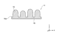
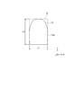
- FIG. 1 is a schematic perspective view of a thin film nanocrystal composite according to the present invention.
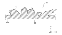
- FIG. 2 is a more detailed schematic perspective view of the thin film nanocrystal composite according to the present invention.
- FIG. 3 is a schematic cross-sectional view showing an II cross section (XY plane) of the schematic perspective view of the thin film nanocrystal composite of FIG.
- FIG. 4 is a more detailed schematic cross-sectional view showing the II cross section (XY plane) of the schematic perspective view of the thin film nanocrystal composite of FIG.
- FIG. 5 is a schematic perspective view showing a region P of the thin film nanocrystal composite in FIG. 1 in an enlarged manner.
- FIG. 6 is a more detailed schematic perspective view showing a region P of the thin film nanocrystal composite of FIG.
- FIG. 7 is a schematic view showing an enlarged view of a nanocrystal piece separated from the thin-film nanocrystal composite shown in FIG. 1 in plan view on the XY plane.
- FIG. 8 is a more detailed schematic view showing a nanocrystal piece separated from the thin film nanocrystal composite of FIG. 2 in an enlarged view in plan view in the XY plane.
- FIG. 9 is an example of an X-ray diffraction spectrum when the structure is analyzed by the nanocrystal composite X-ray diffraction of the present invention.
- FIG. 10 is an observation photograph of the thin-film nanocrystal composite according to Example 1 of the present invention.
- FIG. 11 is an SEM image of the thin film nanocrystal composite according to Example 2 of the present invention.
- FIG. 12 is an SEM image of the powdered nanocrystal piece produced in Comparative Example 1.
- the thin-film nanocrystal composite according to the present invention is formed of a thin-film-like connected assembly in which a plurality of nanocrystal pieces having a main surface and an end face are connected to each other.
- the exposed main surfaces of the plurality of nanocrystal pieces are arranged with a gap, and the connected assembly has a planar view area of 1 mm 2 or more.
- Such a nanocrystal composite is different from conventional nanocrystal materials in the form of powder, and has a macroscopic size of millimeter scale or more by connecting a plurality of nanocrystal pieces to each other. Therefore, in actual use, since it can be used as a thin film-like or sheet-like material, (i) it is possible to selectively cover a portion to be covered of the carrier, and a necessary amount of nanocrystal composite Just prepare. In addition, since (ii) a nanocrystalline composite in the form of a thin film can be attached with an adhesive, for example, when it is assumed to be used as a catalyst, the nanocrystalline composite is formed on a portion (reaction surface) to be supported by a carrier.
- the active surface can be efficiently arranged, and excellent catalytic activity can be realized. Furthermore, (iii) since it is a thin film shape, it is easy to handle and excellent in handling, and (iv) it is easy to clean and isolate after production, and there is no problem such as dissipation, so it can be stored easily.
- FIGS. 1 and 2 show an embodiment of a thin-film nanocrystal composite according to the present invention.
- reference numeral 1 denotes a thin-film nanocrystal composite (hereinafter simply referred to as “nanocrystal composite”). It may be called “body”.)
- 3 and 4 are II sectional views (XY plane) of the thin-film nanocrystal composite 1 shown in FIGS. 1 and 2, respectively.
- 13 is a nanocrystal piece
- 15 is a connecting portion
- 15 a is an exposed portion of the connecting portion 15.
- FIGS. 5 and 6 are schematic perspective views showing an enlarged region P of the thin film nanocrystal composite shown in FIGS. 1 and 2, respectively.
- reference numeral 13 a denotes the main surface of the nanocrystal piece 13
- Reference numeral 13 b denotes an end face of the nanocrystal piece 13.
- the nanocrystal composite 1 of the present invention is in the form of a thin piece, and is a thin film-like connection in which a plurality of nanocrystal pieces having a main surface 13a and an end face 13b are connected to each other. It consists of an assembly 11.
- the connection state of the nanocrystal pieces is not particularly limited, and may be a chemical bond such as crystal growth, an electrical bond such as electrostatic force, or a bond due to accumulation such as intermolecular force.
- the nanocrystal pieces may be connected as a whole to form a thin film aggregate.
- the linked assembly 11 is preferably such that the nanocrystal pieces are linked and integrated by chemical bonding.
- the connection assembly 11 includes a thin-film connection portion 15 having an exposed portion 15 a having a planar view area of 1 mm 2 or more.
- the exposed portion 15a of the connecting portion 15 may be a portion formed by crystal growth of nanocrystal pieces, or may be a portion formed by accumulating nanocrystal pieces.
- Such an exposed part 15a is 1 mm 2 or more in a plan view area, and preferably 100 mm 2 or more.
- the connected assembly 11 having such a millimeter-scale or larger exposed portion 15a is excellent in handleability in actual use.
- assembly 11 is connected to the exposed part 15a of the connection part 15 by each end surface 13b connecting several nanocrystal pieces. , Are arranged at intervals.
- the main surfaces 13a of the plurality of nanocrystal pieces 13 protrude from the exposed portion 15a to the outside of the connection assembly 11, and the main surface 13a is disposed along the surface direction of the thin-film connection portion 15. .
- the main surface 13a protrudes from the exposed portion 15a in a random direction.
- the main surface 13a of the nanocrystal piece 13 faces a random direction.
- Such a linked assembly 11 having a plurality of nanocrystal pieces 13 can exhibit characteristics peculiar to a nanocrystal material while having a size of a millimeter scale or more.
- the connection state of the nanocrystal pieces 13 having the main surface 13 a protruding from the exposed portion 15 a of the connection portion 15 is not particularly limited, and examples thereof include the above-described combined state.
- the nanocrystal pieces 13 are preferably connected to each other by chemical bonding in the connecting portion 15.
- the nanocrystal piece 13 is a part constituting the connected assembly 11 and is in a state where the main surface 13a is connected to the exposed part 15a of the connecting part 15. As shown in FIGS. 5 and 6, such a nanocrystal piece 13 has a thin piece shape and has a main surface 13a and an end face 13b.
- the main surface 13a of the nanocrystal piece 13 is specifically a surface having a large surface area among the outer surfaces constituting the flaky nanocrystal piece 13, and is above and below the end face 13b having a small surface area. It means both surfaces that define the edge.
- the minimum dimension of the main surface 13a of the nanocrystal piece 13 is preferably 1 nm to 2 ⁇ m, and the maximum dimension is preferably 10 nm to 10 ⁇ m. Moreover, it is preferable that the maximum dimension of the end surface of the nanocrystal piece 13 is 1/10 or 10 nm or less of the minimum dimension of the main surface. Moreover, in the nanocrystal piece 13, it is preferable that the ratio of the surface area of the main surface 13a to the end face 13b is 10 times or more in that excellent catalytic activity is obtained, for example, when used as a catalyst. Further, the thickness t of the nanocrystal piece 13 is preferably 0.5 to 100 nm, more preferably 1 to 20 nm. In addition, the minimum dimension of the main surface 13a of the nanocrystal piece 13 is preferably 10 times or more, more preferably 20 times or more of the thickness t in relation to the thickness t.
- the minimum dimension and the maximum dimension of the main surface 13a of the nanocrystal piece 13 measure the nanocrystal piece 13 separated from the connection part 15 as an individual nanocrystal piece so that the shape of the nanocrystal piece 13 is not impaired.
- a rectangle Q having a minimum area that circumscribes the main surface 13a of the nanocrystal piece as the nanocrystal piece 13 is drawn, and the short side L1 and the long side of the rectangle Q are drawn.
- the side L2 is measured as the minimum dimension and the maximum dimension of the nanocrystal piece 13, respectively.
- connection aggregate 11 since the some nanocrystal piece 13 protrudes from the exposed part 15a of the connection part 15, the connection aggregate 11 has a comparatively large specific surface area.
- the specific surface area of such a linked assembly 11 is preferably 5 m 2 / g or more, and more preferably 10 m 2 / g or more.
- the nanocrystal composite 1 composed of such a linked assembly 11 exhibits excellent catalytic activity when used as a catalyst, for example.
- assembly 11 is not specifically limited, The upper limit as a manufacturing or physical limit is 100 m ⁇ 2 > / g, for example.
- the nanocrystal piece constituting the crystal complex 1 of the present invention is preferably constituted of at least one of a metal and a metal oxide.
- the metal include noble metals, transition metals, and alloys containing these metals.
- the noble metal and its alloy are composed of one component selected from the group consisting of palladium (Pd), rhodium (Rh), ruthenium (Ru), platinum (Pt), silver (Ag) and gold (Au). Examples thereof include metals and alloys containing one or more components selected from these groups.
- the transition metal and its alloy are selected from a metal consisting of one component selected from the group of copper (Cu), nickel (Ni), cobalt (Co) and zinc (Zn), or from these groups. Examples include alloys containing one or more components.
- the metal oxide include oxides and composite oxides of noble metals, transition metals, or alloys thereof. Examples of the noble metal and transition metal include those exemplified above.
- the nanocrystal piece is preferably made of a metal oxide containing one or more metals selected from the group of transition metals.
- metal oxides are abundant on the earth as metal resources, and are cheaper than noble metals, and thus are preferable in terms of cost reduction.
- the metal oxide as described above include nickel oxide, copper oxide, Ni—Cu oxide, Cu—Pd oxide, and the like. Among these, copper oxide and Ni—Cu composite oxide are preferable.
- the nanocrystal composite 1 of the present invention is a thin film having a certain size of millimeter order or more, and is an integrated body in which a plurality of nanocrystal pieces are connected to each other. It also exhibits unique properties of nanocrystalline materials. Since such a nanocrystal composite 1 could be handled as a macro thin film of the order of millimeters or more, the nanocrystal material can realize excellent handling properties and workability that are not conventionally provided. On the other hand, it is possible to realize surface properties that could not be realized with conventional metal foils such as electrolytic copper foils, and to exhibit characteristics peculiar to nanocrystalline materials such as nanocrystalline powders while having a thin film shape.
- Such a nanocrystal composite 1 of the present invention can be used for various applications, and can be suitably used as, for example, a catalyst, an electrode material, or an artificial photosynthetic material.
- the nanocrystal composite 1 of the present invention when used as a catalyst, it is not necessary to disperse and embed the nanocrystal composite in an adhesive like a nanocrystal powder when supported on a substrate.
- the active surface can be efficiently arranged on the reaction surface, and the catalyst efficiency is improved.
- the main surface 13a of the nanocrystal piece 13 is an active surface, and thus the main surface 13a of the nanocrystal piece 13 is configured to have a specific crystal orientation. It is preferable.
- a nanocrystal piece is comprised with a metal oxide.
- the main surface 13a of the nanocrystal piece 13 in order to configure the main surface 13a of the nanocrystal piece 13 to be a reducing active surface, in the metal oxide constituting the nanocrystal piece, the surface of the metal atom exhibiting catalytic activity is changed to the main surface.
- the main surface 13a may be composed of a metal atom plane by being oriented so as to be located at 13a. Specifically, the metal atoms occupying the metal atoms and oxygen atoms constituting the metal oxide present on the main surface 13a.
- the number ratio is preferably 80% or more.
- the main surface 13a in order to configure the main surface 13a to be an oxidative active surface, in the metal oxide composing the nanocrystal piece, the surface of the oxygen atom exhibiting catalytic activity is oriented so as to be located on the main surface 13a.
- the main surface 13a may be constituted by an oxygen atom plane.
- the number ratio of oxygen atoms in the metal atoms and oxygen atoms constituting the metal oxide existing on the main surface 13a is 80% or more. It is preferable that
- the main surface 13a is adjusted by adjusting the ratio of the number of metal atoms or oxygen atoms in the metal atoms and oxygen atoms constituting the metal oxide existing on the main surface 13a of the nanocrystal piece 13.
- the catalytic activity function of the nanocrystal 13 can be enhanced, and the nanocrystal piece 13, and thus the nanocrystal composite 1, can exhibit sufficient catalytic activity.
- the main surface 13a of the nanocrystal piece 13 has a specific crystal orientation is that, depending on the type of metal oxide constituting the nanocrystal piece 13, the crystal orientation that exists in the main surface 13a is different. Therefore, the crystal orientation of the main surface 13a is not specifically described.
- the metal oxide is copper oxide (CuO)
- the main crystal orientation of the single crystal constituting the main surface is preferably ⁇ 001 ⁇ .
- the nanocrystal composite 1 has a maximum diffraction angle (2 ⁇ ) of 35.0 to 36.0 degrees in the X-ray diffraction spectrum.
- the peak intensity is I1 and the maximum peak intensity between 38.5 and 40.0 degrees is I2, the peak intensity is preferably I1> I2, more preferably the peak intensity ratio I1 / I2 is 1. It is desirable that the crystal has a degree of crystal orientation that is 0.05 or more, and more preferably has a peak intensity I1 / I2 of 1.2 or more.
- FIG. 9 shows a peak result showing an example of the X-ray diffraction spectrum when the nanocrystal composite 1 of the present invention is subjected to structural analysis by X-ray diffraction. The measurement method will be described on the page of the example.
- the highest peaks I1 and I2 are in the relationship of I1> I2 in terms of peak intensity.
- the highest peak intensity I1 is 35.64 degrees of the crystal plane (002), and the highest peak intensity I2 is It was 39.2 degrees on the (200) plane.
- the maximum peaks I1 and I2 have a peak intensity relationship of I1 ⁇ I2
- the maximum peak intensity I1 is 35.76 degrees of the crystal plane ( ⁇ 111) and the maximum peak intensity I2 is (111). ) Plane of 38.96 degrees.
- the main surface 13a has a metal atomic plane.
- the metal oxide crystal structure is a regular structure in which metal atomic planes and oxygen atomic planes are regularly and alternately stacked, and the arrangement of atoms is regular.
- the main surface 13a is preferably configured such that the metal atomic plane is located.
- the main surface 13a is different not only in the case of a structure composed of an aggregate of single crystals having the same orientation, but is different. Even a structure composed of single crystal aggregates having different crystal structures or different orientations or aggregates including crystal grain boundaries and polycrystals is included when the metal surface is present on the main surface 13a.
- Examples of the method for producing the thin film nanocrystal composite of the present invention include a method for preferentially causing two-dimensional growth of nanocrystal pieces.
- a boundary surface in contact with a boundary where different phases exist such as a gas and a solution, is used as a nucleation priority place. That is, for example, a nanocrystal complex is formed as a thin film on the interface between a gas and a solution, an interface between different types of liquids, or an interface with a substrate (support) placed in the solution.
- a nucleation place is limited and it grows two-dimensionally, it is desirable to manufacture at a temperature lower than a normal hydrothermal method.
- the material of the support base is not particularly limited, and examples thereof include metals, oxides, nitrides, and the like. From the viewpoint of supporting a thin film, Teflon (registered trademark) having excellent chemical resistance at temperatures up to 200 degrees. ) Is desirable.
- Example 1 After mixing 2.0 g of copper chloride (II) dihydrate (manufactured by Junsei Chemical Co., Ltd.) and 1.6 g of urea (manufactured by Junsei Chemical Co., Ltd.), 180 ml of ethylene glycol (manufactured by Junsei Chemical Co., Ltd.) ) And 120 ml of water were added and further mixed. The obtained mixed solution of copper chloride and urea was poured into a pressure resistant glass container having an internal volume of 500 ml, and heat treatment was performed at 150 ° C. for 12 hours in a sealed atmosphere inside the container.
- copper chloride (II) dihydrate manufactured by Junsei Chemical Co., Ltd.
- urea manufactured by Junsei Chemical Co., Ltd.
- 120 ml of water were added and further mixed.
- the obtained mixed solution of copper chloride and urea was poured into a pressure resistant glass container having an internal volume of 500 ml, and heat treatment was performed at 150
- the mixed solution is cooled to room temperature and kept for 1 day, and further, a thin film-shaped precipitate formed from the sealed container is recovered, and this precipitate is washed with methanol and pure water, and is subjected to 70% under vacuum.
- the nanocrystal copper oxide catalyst which consists of the thin film-like connection aggregate
- Example 2 After mixing 1.4 g of copper (II) chloride dihydrate (same as above) and 1.0 g of urea (same as above), 108 ml of ethylene glycol (same as above) and 72 ml of water were added and further mixed.
- the obtained mixed solution of copper chloride and urea was poured into an SUS autoclave hermetically sealed container having an internal volume of 300 ml, and heat treatment was performed in the container at 150 ° C. for 24 hours. Thereafter, the mixed solution is cooled to room temperature and kept for 1 day, and further, a thin film-shaped precipitate formed from the sealed container is recovered, and this precipitate is washed with methanol and pure water, and is subjected to 70% under vacuum.
- the nanocrystal copper oxide catalyst which consists of the thin film-like connection aggregate
- Comparative Example 2 As Comparative Example 2, commercially available copper oxide nanoparticles (544868 Copper (II) oxide manufactured by Sigma Aldrich Japan GK) were prepared and used as a nanocrystalline copper oxide catalyst composed of spherical nanocrystal grains of copper oxide.
- FIG. 10A is an external photograph of a nanocrystalline copper oxide catalyst (area of about 255 mm 2 and weight of 20.06 g) made of a thin film-like connected assembly produced in Example 1, and FIG.
- FIG. 11 is an SEM image at a magnification of 30,000 of the nanocrystalline copper oxide catalyst composed of the thin film-like connected assembly produced in Example 2.
- FIG. 12 is an SEM image when the nanocrystalline copper oxide catalyst composed of powdered nanocrystal pieces prepared in Comparative Example 1 is observed at a magnification of 50,000 times.
- the planar view area of the connecting portion of the connected assembly was calculated by identifying the outline of the connected assembly in the appearance photograph taken from the vertical direction with respect to the surface of the connected assembly, and analyzing the image.
- the thickness and minimum dimensions of the nanocrystal pieces and powdered nanocrystal pieces constituting the linked aggregate, and the particle size of the powdered spherical nanocrystal grains are measured by analyzing SEM images at a magnification of 50,000 times. did.
- the thickness and minimum dimension of the nanocrystal piece were calculated by individualizing the nanocrystal piece so as not to break the shape, observing the individualized nanocrystal piece at the above magnification, and analyzing the SEM image.
- the thickness and minimum dimensions of the nanocrystal pieces and powdered nanocrystal pieces constituting the linked assembly, and the particle size of the powdered spherical nanocrystal grains were arbitrarily selected from 10 nanocrystal pieces and nanocrystal pieces. The value measured and averaged for the crystal grains.
- the take-out rate was 90% or more as an acceptable level.
- Catalyst performance Evaluation of catalyst performance was performed using an apparatus including a gas supply line, a reaction tube, and a gas sampling unit. Specifically, it is as follows. First, 20 mg of the catalyst was charged between the glass filters of the reaction tube. Next, the reaction tube filled with the catalyst was set in the apparatus, and the thermostatic chamber containing the reaction tube was heated from room temperature to 200 ° C. at 10 ° C./min. At this time, reaction tube inlet gas (raw material gas) and reaction tube outlet gas were sampled and subjected to gas analysis to calculate NO conversion rate and CO conversion rate. In addition, the mixed gas of carbon monoxide and nitric oxide (Ar: CO: NO is 98: 1: 1 by mass ratio) was used for source gas.
- the flow rate of the raw material gas is such that the flow rate of each gas (Ar, CO and NO) is measured with a float type flow meter and adjusted with a secondary pressure fluctuation type flow controller valve so that the flow rate of the mixed gas becomes 50 mL / min. Adjusted.
- the material of the reaction tube was quartz glass, and a SUS tube was connected for preheating of the gas supplied to the reaction tube.
- the reaction tube inlet gas and the reaction tube outlet gas were collected from the outlets of the four-way valve and the three-way valve with a 1 L aluminum bag for 20 minutes.
- the collected gas was analyzed using a gas chromatograph (GC-8A, manufactured by Shimadzu Corporation) for nitrogen (N 2 ), nitric oxide (NO), and carbon monoxide (CO), and carbon dioxide (CO 2 ).
- a gas chromatograph (GC-2010, manufactured by Shimadzu Corporation) was used. Further, the NO conversion rate and the CO conversion rate can be calculated from the following formulas (1) from the amounts (ppm) of nitrogen, nitrogen monoxide, carbon monoxide and carbon dioxide in the respective gases collected at the inlet and outlet of the reaction tube. ) And (2).
- NO conversion rate (%) ⁇ N 2 (outlet) ⁇ N 2 (inlet) ⁇ ⁇ 100 / NO (inlet) (1)
- CO conversion rate (%) CO 2 (outlet) ⁇ 100 / CO (raw material gas) (2)
- NO conversion rate and the CO conversion rate were each evaluated as good when 50% or more.
- FIG. 10C and FIG. 11 in Examples 1 and 2, the main surfaces of the plurality of nanocrystal pieces protrude from the exposed portion, and the main surfaces extend along the surface direction of the thin film-like connecting portion. Since it is arranged, it was confirmed to be a thin film-like connected assembly having a certain continuity (Note that FIGS. 10 (a) and (b) are those of Example 1, A similar thin film-like connected assembly was also observed in Example 2). Therefore, in Examples 1 and 2, it was confirmed that it was not a powder of nanocrystal pieces.
- Such a thin-film nanocrystal composite of the present invention adheres to a container or the like to some extent due to the influence of static electricity, but can be collected with tweezers and does not collapse by sampling, and has strength to support its own weight. confirmed.
- the thin film-like crystal composite of the present invention exhibits excellent balanced characteristics in all items of handling property, dissipation resistance and catalyst performance, particularly when used as a catalyst. It has been confirmed that it works.
- the catalyst comprising the thin film nanocrystal composite of the present invention did not change in shape or the like before and after the catalytic reaction, and the stability against the catalytic reaction was also confirmed.
- the catalyst of Comparative Example 1 is configured such that the main surfaces of the plurality of nanocrystal pieces do not protrude from the exposed portion and the powdery nanocrystal pieces are aggregated. It was confirmed that In particular, since the catalyst of Comparative Example 1 is in the form of a powder, there is no continuity between the nanocrystal pieces, and it is impossible to collect in a collective state such as pinching with tweezers. It was confirmed that the film was inferior in terms of handleability compared to the thin film nanocrystal composites of the present invention (Examples 1 and 2), such as scattering and adhesion to containers and the like, which were easily lost. In addition, the catalyst which consists of a powdery nanocrystal piece of the comparative example 1 also did not change the shape etc. before and after the catalytic reaction, and the stability against the catalytic reaction was confirmed.
- the catalyst of Comparative Example 2 is composed of powdered spherical nanocrystal grains. For this reason, in particular, since it is in the form of a powder, it is impossible to collect in a collective state such as pinching with tweezers, as in the case of the nanocrystal piece of Comparative Example 1. It was confirmed that the film was inferior in terms of handleability compared to the thin film nanocrystal composites of the present invention (Examples 1 and 2), such as adhesion to a container and the like, which was easily lost.
- the catalysts of Comparative Examples 1 and 2 are in powder form, they are inferior to the thin film nanocrystal composites of the present invention (Examples 1 and 2) from the viewpoint of dissipation resistance and removal rate. It was confirmed that Furthermore, the catalysts of Comparative Examples 1 and 2 were significantly inferior to the thin-film nanocrystal composites of the present invention (Examples 1 and 2) in terms of NO conversion ratio among the catalyst performances. Further, the catalyst of Comparative Example 2 was inferior to Examples 1 and 2 not only in NO conversion rate but also in CO conversion rate. Further, in the catalyst of Comparative Example 2, the powder was dissipated and partially changed to copper before and after the catalytic reaction, and in particular, the dissipating property and the instability to the catalytic reaction were confirmed.
Landscapes
- Chemical & Material Sciences (AREA)
- Engineering & Computer Science (AREA)
- Organic Chemistry (AREA)
- Chemical Kinetics & Catalysis (AREA)
- Materials Engineering (AREA)
- Environmental & Geological Engineering (AREA)
- General Chemical & Material Sciences (AREA)
- Health & Medical Sciences (AREA)
- Biomedical Technology (AREA)
- Analytical Chemistry (AREA)
- Oil, Petroleum & Natural Gas (AREA)
- Inorganic Chemistry (AREA)
- Thermal Sciences (AREA)
- Combustion & Propulsion (AREA)
- Physics & Mathematics (AREA)
- Catalysts (AREA)
- Crystallography & Structural Chemistry (AREA)
Abstract
本発明は、ナノ結晶材料としての特性(例えば優れた触媒活性等)を良好に維持しつつ、上記のような粉末形状のナノ結晶材料の問題点を解決した、取り扱い性に優れたナノ結晶材料としての薄膜状ナノ結晶複合体を提供することを目的とする。 薄片状をなし、主表面および端面をもつ複数のナノ結晶片が相互に連結された、薄膜状の連結集合体からなり、前記連結集合体の外側に露出する、前記複数のナノ結晶片の前記主表面が間隙を有して配置され、前記連結集合体が、1mm2以上の平面視面積を有することを特徴とする、薄膜状ナノ結晶複合体。
Description
本発明は、取り扱い性に優れた薄膜状のナノ結晶複合体に関する。
ナノ結晶材料は、触媒や、電極材料等に様々な分野で広く用いられている。近年、ナノ結晶材料では、ナノメートルスケールの粒径をもつナノ粒子として、さらなる微細化や、活性面の制御等の検討が積極的に行われている。
例えば特許文献1では、特定の単結晶の特定な面を一面とするナノ単結晶板材を、隣接するナノ単結晶板材間で触媒活性面同士を接面させることなく集積したナノ単結晶板材集積触媒(ナノフラワー)が提案されている。また特許文献1には、ナノ単結晶板材集積触媒を用いることによって、熱凝集しても、触媒活性面同士が接面されることがなく、触媒活性面の前にスペース(空隙部)が確保され、熱凝集による触媒活性の低下を抑制でき、触媒活性を高くすることができ、さらに、ナノ単結晶板材を、触媒活性面を(001)面とする、遷移金属酸化物であるCuOのナノ単結晶板材とすることによって、触媒の材料コストを低減できることが記載されている。
しかし、特許文献1記載のナノ単結晶板材集積触媒や、一般的なナノ結晶粉末は、粒径がナノスケール(20~200nm程度)であるため、実際の使用にあたっては、取り扱い性に問題があった。
例えば、次のような取り扱い性の問題が挙げられる。(i)粉末形状のナノ結晶材料は、そのままの状態では使用できないため、接着剤等を用いて、一定の大きさをもつ担体に固定する必要がある。その際、担持されるナノ結晶材料の量の10倍以上の材料を準備する必要があり、これは材料ロスの問題となる。また、(ii)担持するにあたっては接着剤に粉末形状のナノ結晶材料を分散させて埋め込むことになるため、例えば触媒としての使用を想定した場合には、担持した面に、ナノ結晶材料の活性面が効率的に配置できず、ナノ結晶材料としての触媒活性を十分に発揮できないという問題がある。さらに、(iii)粉末形状のナノ結晶材料は、微細であるため、飛散防止等の観点でその取り扱いに際して特殊な治具や設備が必要となるという問題がある。また、(iv)このような微細なナノ結晶材料は、製造後の洗浄や単離が煩雑であるほか、微細な状態での保管が困難で散逸の問題もある。
本発明は、上記実情に鑑みてなされたものであり、ナノ結晶材料としての特性(例えば優れた触媒活性等)を良好に維持しつつ、上記のような粉末形状のナノ結晶材料の問題点を解決した、取り扱い性に優れたナノ結晶材料としての薄膜状ナノ結晶複合体を提供することを目的とする。
本発明者らは、新規のナノ結晶複合体について鋭意研究を重ねた結果、薄膜状ナノ結晶複合体が、薄片状をなし、主表面および端面をもつ複数のナノ結晶片が相互に連結された、薄膜状の連結集合体からなり、前記連結集合体の外側に露出する、前記複数のナノ結晶片の前記主表面が間隙を有して配置され、前記連結集合体が、1mm2以上の平面視面積を有することによって、特に、ナノ(メートル)スケールの特性を維持しつつ、ミリ(メートル)スケール以上の優れた取り扱い性を実現し得ることを見出し、かかる知見に基づき本発明を完成させるに至った。
すなわち、本発明の要旨構成は、以下のとおりである。
[1] 薄片状をなし、主表面および端面をもつ複数のナノ結晶片が相互に連結された、薄膜状の連結集合体からなり、
前記連結集合体の外側に露出する、前記複数のナノ結晶片の前記主表面が間隙を有して配置され、
前記連結集合体が、1mm2以上の平面視面積を有することを特徴とする、薄膜状ナノ結晶複合体。
[2] 前記ナノ結晶片は、厚さが0.5~100nmであり、かつ主表面の最小寸法が前記厚さの10倍以上である、上記[1]に記載の薄膜状ナノ結晶複合体。
[3] 前記平面視面積が100mm2以上である、上記[1]または[2]に記載の薄膜状ナノ結晶複合体。
[4] 比表面積が5m2/g以上である、上記[1]~[3]のいずれか1つに記載の薄膜状ナノ結晶複合体。
[5] 前記ナノ結晶片は、酸化銅で構成されており、
X線回折スペクトルの回折角度(2θ)にて、35.0~36.0度の間の最高ピーク強度をI1とし、38.5~40.0度の間の最高ピーク強度をI2としたときに、ピーク強度比I1/I2が1.05以上である結晶配向度を有する、上記[1]~[4]のいずれか1つに記載の薄膜状ナノ結晶複合体。
本発明によれば、ナノスケールの特性を維持しつつ、ミリスケール以上の優れた取り扱い性を実現し得る、薄膜状ナノ結晶複合体を提供することができる。
<薄膜状ナノ結晶複合体>
本発明に従う薄膜状ナノ結晶複合体は、薄片状をなし、主表面および端面をもつ複数のナノ結晶片が相互に連結された、薄膜状の連結集合体からなり、前記連結集合体の外側に露出する、前記複数のナノ結晶片の前記主表面が間隙を有して配置され、前記連結集合体が、1mm2以上の平面視面積を有することを特徴とする。
本発明に従う薄膜状ナノ結晶複合体は、薄片状をなし、主表面および端面をもつ複数のナノ結晶片が相互に連結された、薄膜状の連結集合体からなり、前記連結集合体の外側に露出する、前記複数のナノ結晶片の前記主表面が間隙を有して配置され、前記連結集合体が、1mm2以上の平面視面積を有することを特徴とする。
このようなナノ結晶複合体は、従来の粉末形状のナノ結晶材料とは異なり、複数のナノ結晶片が相互に連結されてミリスケール以上のマクロな大きさを有している。そのため、実際の使用にあたっては、薄膜形状やシート形状の材料のような使用が可能となるため、(i)担体の覆いたい部分を選択的に覆うことができ、必要な分量のナノ結晶複合体を準備すればよい。また、(ii)薄膜形状のナノ結晶複合体を接着剤で貼り付けて使用できるため、例えば触媒としての使用を想定した場合には、担体の担持したい部分(反応面)に、ナノ結晶複合体の活性面を効率的に配置でき、優れた触媒活性を実現できる。さらに、(iii)薄膜形状なので取り扱いが容易で、取り回し性に優れ、(iv)製造後の洗浄や単離も容易であるほか、散逸等の問題もないので保管も容易である。
図1、2は、本発明に従う薄膜状ナノ結晶複合体の一実施形態を示したものであって、図1、2中、符号1は薄膜状ナノ結晶複合体(以下、単に「ナノ結晶複合体」ということがある。)である。また、図3、4は、それぞれ、図1、2に示す薄膜状ナノ結晶複合体1のI-I断面図(X-Y面)であって、図3、4中、符号11は連結集合体、13はナノ結晶片、15は連結部、15aは連結部15の表出部である。図5、6は、それぞれ、図1、2の薄膜状ナノ結晶複合体の領域Pを拡大して示す概略斜視図あって、図5、6中、符号13aはナノ結晶片13の主表面、13bはナノ結晶片13の端面である。
図1~図6に示されるように、本発明のナノ結晶複合体1は、薄片状をなし、主表面13aおよび端面13bをもつ複数のナノ結晶片が相互に連結された、薄膜状の連結集合体11からなる。ナノ結晶片の連結状態は特に限定されず、結晶成長のような化学的な結合であってもよいし、静電気力のような電気的な結合や、分子間力のような集積による結合であってもよく、全体としてナノ結晶片が連結して薄膜状の集合体を形成していればよい。特に、連結集合体11は、ナノ結晶片同士が互いに化学的な結合により連結一体化されていることが好ましい。
また、図3、4に示されるように、連結集合体11は、1mm2以上の平面視面積の表出部15aをもつ、薄膜状の連結部15を有する。連結部15の表出部15aは、ナノ結晶片が結晶成長してできた部位であってもよいし、ナノ結晶片が集積してできた部位であってもよい。このような表出部15aは、平面視面積で1mm2以上であり、好ましくは100mm2以上である。このようなミリスケール以上の表出部15aをもつ、連結集合体11は、実際の使用に際しての取り扱い性に優れる。
また、連結部15の表出部15aには、複数のナノ結晶片がそれぞれの端面13bで連結されることで連結集合体11の外側に露出した、それぞれのナノ結晶片13の主表面13aが、間隔を有して配置されている。複数のナノ結晶片13の主表面13aは、表出部15aから連結集合体11の外方向へ突出しており、主表面13aは、薄膜状の連結部15の面方向に沿って配置されている。また、主表面13aは、表出部15aからランダムな方向へ突出している。さらに、ナノ結晶片13の主表面13aは、ランダムな方向を向いている。このような複数のナノ結晶片13を有する連結集合体11は、ミリスケール以上の大きさでありながら、ナノ結晶材料特有の特性を発揮し得る。このような連結集合体11において、連結部15の表出部15aから突出している主表面13aを有するナノ結晶片13の連結状態は、特に限定されず、上述のような結合状態が挙げられるが、特に、連結部15におけるナノ結晶片13の結合強度を高める観点からは、ナノ結晶片13は連結部15において化学的な結合により相互に連結されていることが好ましい。
ここでナノ結晶片13は、連結集合体11を構成する部分であって、連結部15の表出部15aに、主表面13aが連結されている状態である。このようなナノ結晶片13は、図5、6に示されるように、薄片状をなし、主表面13aおよび端面13bをもつ。ここで、ナノ結晶片13の主表面13aとは、具体的には、薄片状のナノ結晶片13を構成する外面のうち、表面積が広い面のことであって、表面積が狭い端面13bの上下端縁を区画形成する両表面のことを意味する。ナノ結晶片13の主表面13aの最小寸法は1nm~2μmであることが好ましく、最大寸法は10nm~10μmであることが好ましい。また、ナノ結晶片13の端面の最大寸法は、主表面の最小寸法の1/10もしくは10nm以下であることが好ましい。また、ナノ結晶片13において、主表面13aの端面13bに対する表面積の割合は、10倍以上であることが、例えば触媒として用いた場合に優れた触媒活性を奏する点で好ましい。また、ナノ結晶片13の厚さtは、好ましくは0.5~100nmであり、より好ましくは1~20nmである。また、ナノ結晶片13の主表面13aの最小寸法は、厚さtとの関係では、厚さtの10倍以上であることが好ましく、より好ましくは20倍以上である。
なお、ナノ結晶片13の主表面13aの最小寸法および最大寸法は、ナノ結晶片13の形状を損なわないように、連結部15から分離したナノ結晶片13を、個別のナノ結晶片として測定することにより求める。具体的には、例えば図7、8に示されるように、ナノ結晶片13としてのナノ結晶片の主表面13aに対し、外接する最小面積の長方形Qを描き、長方形Qの短辺L1および長辺L2を、ナノ結晶片13の最小寸法および最大寸法としてそれぞれ測定する。なお、具体的な測定方法は、実施例の頁にて説明する。
また、連結集合体11は、連結部15の表出部15aから複数のナノ結晶片13が突出しているため、比表面積が比較的大きい。このような連結集合体11の比表面積は、5m2/g以上であることが好ましく、10m2/g以上であることがより好ましい。このような連結集合体11からなるナノ結晶複合体1は、例えば触媒として用いた場合に、優れた触媒活性を発揮する。なお、連結集合体11の比表面積の上限は特に限定しないが、製造上または物理上の限界としての上限は、例えば、100m2/gである。
本発明の結晶複合体1を構成するナノ結晶片は、金属および金属酸化物の少なくとも一方で構成されることが好ましい。
ここで、金属としては、例えば、貴金属や、遷移金属、これらの金属を含む合金が挙げられる。特に、貴金属およびその合金としては、パラジウム(Pd)、ロジウム(Rh)、ルテニウム(Ru)、白金(Pt)、銀(Ag)および金(Au)の群から選択される1種の成分からなる金属またはこれらの群から選択される1種以上の成分を含む合金が挙げられる。また、遷移金属およびその合金としては、銅(Cu)、ニッケル(Ni)、コバルト(Co)および亜鉛(Zn)の群から選択される1種の成分からなる金属またはこれらの群から選択される1種以上の成分を含む合金が挙げられる。
また、金属酸化物としては、例えば、貴金属、遷移金属またはそれらの合金の酸化物や複合酸化物等が挙げられる。貴金属や遷移金属は上記で例示したもの等が挙げられる。
特にナノ結晶片は、遷移金属の群から選択される1種または2種以上の金属を含む金属酸化物からなることが好ましい。このような金属酸化物は、金属資源として地球上に豊富に存在しており、貴金属に比べて安価であることから、価格を抑える点で好ましい。中でも、Cu、Ni、CoおよびZnの群から選択される1種または2種以上の金属を含む金属酸化物からなることが好ましく、このような金属酸化物は少なくとも銅を含むことがより好ましい。また、上記のような金属酸化物としては、例えば、酸化ニッケル、酸化銅、Ni-Cu酸化物、Cu-Pd酸化物等が挙げられ、中でも酸化銅、Ni-Cu複合酸化物が好ましい。
以上説明してきたように、本発明のナノ結晶複合体1は、ミリオーダー以上の一定の大きさをもつ薄膜状でありながら、複数のナノ結晶片が相互に連結された集積体であるため、ナノ結晶材料特有の特性も発揮する。このようなナノ結晶複合体1は、ミリオーダー以上のマクロな薄膜として取り扱うことができたため、ナノ結晶材料として、従来にはない優れた取り扱い性や作業性を実現できる。一方で、電解銅箔のような従来の金属箔等では実現できなかった表面性状を実現でき、薄膜形状でありながらナノ結晶粉末のようなナノ結晶材料特有の特性を発揮し得る。
このような本発明のナノ結晶複合体1は、様々な用途に用いることができるが、例えば触媒や、電極材料、人工光合成材料として好適に用いることができる。
特に、本発明のナノ結晶複合体1を触媒として用いる場合には、基材に担持する際に、ナノ結晶粉末のように接着剤中に分散させて埋め込む必要がないため、ナノ結晶複合体の活性面を効率的に反応表面に配置でき、触媒効率が向上する。
このような触媒としての本発明のナノ結晶複合体1では、ナノ結晶片13の主表面13aが活性表面となるため、ナノ結晶片13の主表面13aが特定の結晶方位を有するように構成することが好ましい。また、ナノ結晶複合体1を触媒として用いる場合には、ナノ結晶片は金属酸化物により構成されることが好ましい。
ここで、ナノ結晶片13の主表面13aが還元性の活性面になるように構成するには、ナノ結晶片を構成する金属酸化物において、触媒活性を発揮する金属原子の面を、主表面13aに位置するように配向させて、主表面13aを金属原子面で構成すればよく、具体的には、主表面13aに存在する金属酸化物を構成する、金属原子および酸素原子に占める金属原子の個数割合を80%以上とすることが好ましい。
また主表面13aが酸化性の活性面になるように構成するには、ナノ結晶片を構成する金属酸化物において、触媒活性を発揮する酸素原子の面を、主表面13aに位置するように配向させて、主表面13aを酸素原子面で構成すればよく、具体的には、主表面13aに存在する金属酸化物を構成する、金属原子および酸素原子に占める酸素原子の個数割合を80%以上とすることが好ましい。
活性面の役割に応じて、ナノ結晶片13の主表面13aに存在する金属酸化物を構成する、金属原子および酸素原子に占める金属原子または酸素原子の個数割合を調整することにより、主表面13aの触媒活性機能を高めることができ、ナノ結晶片13、ひいてはナノ結晶複合体1として、十分な触媒活性を発揮できる。
また、ナノ結晶片13の主表面13aが特定の結晶方位を有するとしたのは、ナノ結晶片13を構成する金属酸化物の種類に応じて、主表面13aに多く存在する結晶方位が異なるためであり、このため、主表面13aの結晶方位は具体的には記載はしない。例えば、金属酸化物が酸化銅(CuO)の場合には、主表面を構成する単結晶の主な結晶方位は{001}であることが好ましい。
また、ナノ結晶片13が酸化銅(CuO)で構成されている場合、このナノ結晶複合体1は、X線回折スペクトルの回折角度(2θ)の35.0~36.0度の間の最高ピーク強度をI1とし、38.5~40.0度の間の最高ピーク強度をI2としたときに、ピーク強度がI1>I2であることが好ましく、より好ましくはピーク強度比I1/I2が1.05以上であり、さらに好ましくはピーク強度がI1/I2が1.2以上である、結晶配向度を有することが望ましい。
図9に、本発明のナノ結晶複合体1をX線回折で構造分析を行なった際の、X線回折スペクトルの一例を示すピークの結果を示す。なお、測定方法については、実施例の頁にて説明する。
図9では、上記最高ピークI1とI2とが、ピーク強度でI1>I2の関係にあり、このとき、最高ピーク強度I1は、結晶面(002)の35.64度、最高ピーク強度I2は、(200)面の39.2度であった。
また一方で、上記最高ピークI1とI2とが、ピーク強度でI1<I2の関係である場合、最高ピーク強度I1は結晶面(-1 11)の35.76度、最高ピーク強度I2は(111)面の38.96度となる。
すなわち上記最高ピークI1とI2とが、I1>I2であり、かつピーク強度比I1/I2が1.05以上の場合、ナノ結晶複合体1の表面の酸化銅ナノ結晶(すなわち、ナノ結晶片13を構成する酸化銅ナノ結晶)は、触媒性能に有効な活性面である(002)に配向しており、高い触媒性能を発揮し得る。
また一方で、上記最高ピークI1とI2とが、ピーク強度でI1<I2の関係である場合、最高ピーク強度I1は結晶面(-1 11)の35.76度、最高ピーク強度I2は(111)面の38.96度となる。
すなわち上記最高ピークI1とI2とが、I1>I2であり、かつピーク強度比I1/I2が1.05以上の場合、ナノ結晶複合体1の表面の酸化銅ナノ結晶(すなわち、ナノ結晶片13を構成する酸化銅ナノ結晶)は、触媒性能に有効な活性面である(002)に配向しており、高い触媒性能を発揮し得る。
また、主表面13aを金属原子面とする構成としては、金属酸化物の結晶構造を、金属原子面と酸素原子面が規則的に交互に積層され、原子の並び方に規則性を有する規則構造として、主表面13aに金属原子面が位置するように構成することが好ましく、具体的には、主表面13aが、同じ配向をもつ単結晶の集合体で構成された構造の場合だけではなく、異なる結晶構造や異なる配向をもつ単結晶の集合体や、結晶粒界や多結晶を含んだ集合体で構成された構造であっても、主表面13aに金属原子面が存在する場合は含まれる。
<薄膜状ナノ結晶複合体の製造方法>
本発明の薄膜状ナノ結晶複合体の製造方法としては、例えば、ナノ結晶片の二次元成長を優先的に起こす方法が挙げられる。このような方法では、例えば気体と溶液の間のような、異なる相が存在する境界に接する境界面を、核生成優先場所として利用する。すなわち、例えば気体と溶液の境界面、異なる種類の液体の界面、または溶液中に配置した基材(支持台)との界面等に、薄膜としてナノ結晶複合体を形成する。なお、本発明の製造方法では、核生成場所を限定して二次元成長させるので、通常の水熱法よりは低い温度で製造することが望ましい。
本発明の薄膜状ナノ結晶複合体の製造方法としては、例えば、ナノ結晶片の二次元成長を優先的に起こす方法が挙げられる。このような方法では、例えば気体と溶液の間のような、異なる相が存在する境界に接する境界面を、核生成優先場所として利用する。すなわち、例えば気体と溶液の境界面、異なる種類の液体の界面、または溶液中に配置した基材(支持台)との界面等に、薄膜としてナノ結晶複合体を形成する。なお、本発明の製造方法では、核生成場所を限定して二次元成長させるので、通常の水熱法よりは低い温度で製造することが望ましい。
ここで、二次元方向への成長を誘導する観点から、溶液内の、気体と溶液の境界面下方に支持台を設置することが望ましい。支持台の材質としては、特に限定しないが、例えば、金属や酸化物、窒化物等が挙げられ、また薄膜の支持の観点から、200度までの温度で、耐薬品性に優れるテフロン(登録商標)が望ましい。
以上、本発明の実施形態について説明したが、本発明は上記実施形態に限定されるものではなく、本発明の概念および請求の範囲に含まれるあらゆる態様を含み、本発明の範囲内で種々に改変することができる。
次に、本発明の効果をさらに明確にするために、実施例および比較例について説明するが、本発明はこれら実施例に限定されるものではない。
(実施例1)
2.0gの塩化銅(II)二水和物(純正化学株式会社製)と、1.6gの尿素(純正化学株式会社製)とを混合した後、180mlのエチレングリコール(純正化学株式会社製)と120mlの水を添加してさらに混合した。得られた塩化銅と尿素の混合溶液を、内容積500mlの耐圧硝子容器に注入し、該容器内の密閉雰囲気下で150℃、12時間の熱処理を行った。
その後、混合溶液を、室温に冷却して1日保持した後、さらに密閉容器から生成した薄膜形状の沈殿物を回収し、この沈殿物を、メタノールおよび純水で洗浄して、真空下、70℃で10時間真空乾燥させ、銅酸化物のナノ結晶片が連結された薄膜状の連結集合体からなるナノ結晶銅酸化物触媒を得た。
(実施例2)
1.4gの塩化銅(II)二水和物(同上)と1.0gの尿素(同上)とを混合した後、108mlのエチレングリコール(同上)と72mlの水を添加してさらに混合した。得られた塩化銅と尿素の混合溶液を、内容積300mlのSUS製のオートクレーブ密閉容器に注入し、該容器内で150℃、24時間の熱処理を行った。
その後、混合溶液を、室温に冷却して1日保持した後、さらに密閉容器から生成した薄膜形状の沈殿物を回収し、この沈殿物を、メタノールおよび純水で洗浄して、真空下、70℃で10時間真空乾燥させ、銅酸化物のナノ結晶片が連結された薄膜状の連結集合体からなるナノ結晶銅酸化物触媒を得た。
1.4gの塩化銅(II)二水和物(同上)と1.0gの尿素(同上)とを混合した後、108mlのエチレングリコール(同上)と72mlの水を添加してさらに混合した。得られた塩化銅と尿素の混合溶液を、内容積300mlのSUS製のオートクレーブ密閉容器に注入し、該容器内で150℃、24時間の熱処理を行った。
その後、混合溶液を、室温に冷却して1日保持した後、さらに密閉容器から生成した薄膜形状の沈殿物を回収し、この沈殿物を、メタノールおよび純水で洗浄して、真空下、70℃で10時間真空乾燥させ、銅酸化物のナノ結晶片が連結された薄膜状の連結集合体からなるナノ結晶銅酸化物触媒を得た。
(比較例1)
2.0gの塩化銅(II)二水和物(同上)と1.4gの尿素(同上)とを混合した後、160mlのエチレングリコール(同上)と240mlの水を添加してさらに混合した。得られた塩化銅と尿素の混合溶液を、内容積500mlのSUS製のオートクレーブ密閉容器に注入し、該容器内で180℃、36時間の熱処理を行った。
その後、混合溶液を、室温に冷却した後、密閉容器から取り出した。さらに、混合溶液中に生成した沈殿物を回収し、この沈殿物を、メタノールおよび純水で洗浄し真空下、70℃で10時間真空乾燥させ、銅酸化物のナノ結晶片(粉末状)からなるナノ結晶銅酸化物触媒を得た。
2.0gの塩化銅(II)二水和物(同上)と1.4gの尿素(同上)とを混合した後、160mlのエチレングリコール(同上)と240mlの水を添加してさらに混合した。得られた塩化銅と尿素の混合溶液を、内容積500mlのSUS製のオートクレーブ密閉容器に注入し、該容器内で180℃、36時間の熱処理を行った。
その後、混合溶液を、室温に冷却した後、密閉容器から取り出した。さらに、混合溶液中に生成した沈殿物を回収し、この沈殿物を、メタノールおよび純水で洗浄し真空下、70℃で10時間真空乾燥させ、銅酸化物のナノ結晶片(粉末状)からなるナノ結晶銅酸化物触媒を得た。
(比較例2)
比較例2として市販の酸化銅ナノ粒子(シグマ アルドリッチ ジャパン合同会社製 544868 Copper(II) oxide)を準備し、これを銅酸化物の球状ナノ結晶粒からなるナノ結晶銅酸化物触媒とした。
比較例2として市販の酸化銅ナノ粒子(シグマ アルドリッチ ジャパン合同会社製 544868 Copper(II) oxide)を準備し、これを銅酸化物の球状ナノ結晶粒からなるナノ結晶銅酸化物触媒とした。
[評価]
上記実施例および比較例に係る触媒を用いて、下記に示す特性評価を行った。各特性の評価条件は下記の通りである。結果を表1に示す。
上記実施例および比較例に係る触媒を用いて、下記に示す特性評価を行った。各特性の評価条件は下記の通りである。結果を表1に示す。
[1]組織観察
組織観察は、マイクロスコープ(株式会社キーエンス製)および走査型電子顕微鏡(SEM、日本電子株式会社製)を用いて行った。マイクロスコープ観察では、膜全体の全体外観と、膜としての連続性を確認した。また、SEM観察では、ナノ結晶の組織を確認した。なお、図10~12に、実施例1および2、並びに比較例1の観察結果を、写真として示す。特に図10(a)は、実施例1で作製した薄膜状の連結集合体からなるナノ結晶銅酸化物触媒(面積約255mm2、重さ20.06g)の外観写真であり、(b)は倍率100倍で観察した際のSEM画像であり、(c)は倍率5万倍で観察した際のSEM画像である。また、図11は、実施例2で作製した薄膜状の連結集合体からなるナノ結晶銅酸化物触媒の倍率3万のSEM画像である。さらに図12は、比較例1で作製した粉末状のナノ結晶片からなるナノ結晶銅酸化物触媒を、倍率5万倍で観察した際のSEM画像である。
組織観察は、マイクロスコープ(株式会社キーエンス製)および走査型電子顕微鏡(SEM、日本電子株式会社製)を用いて行った。マイクロスコープ観察では、膜全体の全体外観と、膜としての連続性を確認した。また、SEM観察では、ナノ結晶の組織を確認した。なお、図10~12に、実施例1および2、並びに比較例1の観察結果を、写真として示す。特に図10(a)は、実施例1で作製した薄膜状の連結集合体からなるナノ結晶銅酸化物触媒(面積約255mm2、重さ20.06g)の外観写真であり、(b)は倍率100倍で観察した際のSEM画像であり、(c)は倍率5万倍で観察した際のSEM画像である。また、図11は、実施例2で作製した薄膜状の連結集合体からなるナノ結晶銅酸化物触媒の倍率3万のSEM画像である。さらに図12は、比較例1で作製した粉末状のナノ結晶片からなるナノ結晶銅酸化物触媒を、倍率5万倍で観察した際のSEM画像である。
ここで、連結集合体の連結部の平面視面積は、連結集合体の表面に対し鉛直方向から撮影した外観写真において、連結集合体の輪郭を特定し、画像解析することにより算出した。
また、連結集合体を構成するナノ結晶片と粉末状のナノ結晶片の厚さおよび最小寸法、並びに粉末状の球状ナノ結晶粒の粒径は、倍率5万倍のSEM画像を解析して測定した。特に、ナノ結晶片の厚さおよび最小寸法は、ナノ結晶片の形状を壊さないように個別化し、個別化したナノ結晶片を上記倍率で観察し、SEM画像を解析して算出した。
なお、連結集合体を構成するナノ結晶片と粉末状のナノ結晶片の厚さおよび最小寸法、並びに粉末状の球状ナノ結晶粒の粒径は、任意に選択した10個のナノ結晶片およびナノ結晶粒について測定し、平均した値である。
また、連結集合体を構成するナノ結晶片と粉末状のナノ結晶片の厚さおよび最小寸法、並びに粉末状の球状ナノ結晶粒の粒径は、倍率5万倍のSEM画像を解析して測定した。特に、ナノ結晶片の厚さおよび最小寸法は、ナノ結晶片の形状を壊さないように個別化し、個別化したナノ結晶片を上記倍率で観察し、SEM画像を解析して算出した。
なお、連結集合体を構成するナノ結晶片と粉末状のナノ結晶片の厚さおよび最小寸法、並びに粉末状の球状ナノ結晶粒の粒径は、任意に選択した10個のナノ結晶片およびナノ結晶粒について測定し、平均した値である。
[2]X線回折による結晶配向性測定
X線回折装置(D8 DISCOVER、ブルカー・エイエックスエス株式会社製)による構造分析を行なった。X線回折で、各触媒の組成の同定を行い、酸化銅(CuO)単体であることを確認した。さらに、X線回折スペクトルの回折角度(2θ)の35.0~36.0度の間の最高ピーク強度をI1とし、38.5~40.0度の間の最高ピーク強度をI2としたときの、ピーク強度比I1/I2を、結晶配向度として求めた。
X線回折装置(D8 DISCOVER、ブルカー・エイエックスエス株式会社製)による構造分析を行なった。X線回折で、各触媒の組成の同定を行い、酸化銅(CuO)単体であることを確認した。さらに、X線回折スペクトルの回折角度(2θ)の35.0~36.0度の間の最高ピーク強度をI1とし、38.5~40.0度の間の最高ピーク強度をI2としたときの、ピーク強度比I1/I2を、結晶配向度として求めた。
[3]比表面積測定
JIS Z 8830:2013に準拠したBET法により、高精度・多検体ガス吸着量測定装置(AutoSorb-iQ2、カンタクローム・インスツルメンツ・ジャパン合同会社製)で、窒素ガスを用いて測定した。なお、前処理条件として、200℃で3時間の真空脱気した後に、測定した。
JIS Z 8830:2013に準拠したBET法により、高精度・多検体ガス吸着量測定装置(AutoSorb-iQ2、カンタクローム・インスツルメンツ・ジャパン合同会社製)で、窒素ガスを用いて測定した。なお、前処理条件として、200℃で3時間の真空脱気した後に、測定した。
[4]取り出し率の測定(取り扱い性)
取り扱い性を評価するために、次の方法で取り出し率を測定した。
まず、長さ200mmのガラス試験管にガラスウール20mgを詰め、触媒を5mg秤量して上記試験管内のガラスウール上に載せ、さらに触媒上にガラスウール20mgを詰める。その後、すべてのガラスウールと、触媒を上記試験管から取り出し、薬包紙に並べ、再度、同じ手順で一度取り出したガラスウールと触媒を上記試験管に詰めた。そして、すべてのガラスウールと、触媒を上記試験管から取り出し、2度目に取り出された触媒の重量を測定し、最初に秤量した触媒の重量に対する比率(2度目に取り出された触媒の重量×100/最初に秤量した触媒の重量)を求め、取り出し率(%)として評価した。本実施例では、取り出し率が90%以上を合格レベルとした。
[5]回収率の測定(耐散逸性)
耐散逸性を評価するために、次の方法で回収率を測定した。
まず、触媒10mgをガラスウールに分散させ、アルゴン(Ar)ガスを充填した密閉ガラス容器内に入れて、200℃に加熱後、該容器内に一酸化炭素(CO)と一酸化窒素(NO)の混合ガス(Ar:CO:NOが質量比で98:1:1)を導入し、該容器内のガスを上記混合ガスに置換し、触媒反応を行った。その後、触媒を、上記ガラス容器から取り出し、ガラスウールから分離して、回収した触媒の重量を測定した。最初に秤量した触媒の重量に対する比率(回収した触媒の重量×100/最初に秤量した触媒の重量)を求め、回収率(%)として評価した。本実施例では、回収率が90%以上を合格レベルとした。
[6]触媒性能
触媒性能の評価は、ガス供給ライン、反応管およびガスサンプリング部よりなる装置を用いて行った。具体的には以下の通りである。
まず、反応管のガラスフィルタの間に、触媒を20mg充填した。次に、触媒を充填した反応管を、装置にセットし、反応管が入っている恒温槽を室温から200℃まで10℃/minで昇温した。このとき反応管入口ガス(原料ガス)および反応管出口ガスを採取し、ガス分析を行い、NO転換率およびCO転換率を算出した。
なお、原料ガスは、一酸化炭素と一酸化窒素の混合ガス(Ar:CO:NOが質量比で98:1:1)を用いた。原料ガスの流量は、各ガス(Ar、COおよびNO)の流量をフロート式流量計で計測し、二次圧変動型フローコントローラバルブで調節して、混合ガスの流量で50mL/minとなるように調節した。また、反応管の材質は石英ガラスであり、反応管へ供給するガスの予備加熱にはSUS管を接続して用いた。
また、反応管入口ガスおよび反応管出口ガスの採取は、四方バルブおよび三方バルブの出口から、1Lアルミニウムバッグで、20分間行った。採取したガスの分析は、窒素(N2)、一酸化窒素(NO)および一酸化炭素(CO)にはガスクロマトグラフ(GC-8A、株式会社島津製作所製)を用い、二酸化炭素(CO2)にはガスクロマトグラフ(GC-2010、株式会社島津製作所製)を用いた。さらにNO転換率およびCO転換率は、上記反応管の入口および出口で採取されたそれぞれのガス中の窒素、一酸化窒素、一酸化炭素および二酸化炭素の各量(ppm)から、下記式(1)および(2)により算出した。
NO転換率(%)={N2(出口)-N2(入口)}×100/NO(入口)・・・(1)
CO転換率(%)=CO2(出口)×100/CO(原料ガス)・・・(2)
本実施例では、NO転換率およびCO転換率がそれぞれ50%以上を良好と評価した。

図10(c)および図11に示されるように、実施例1および2では、複数のナノ結晶片の主表面が表出部から突出し、主表面は薄膜状の連結部の面方向に沿って配置されていることから、一定の連続性をもった薄膜状の連結集合体であることが確認された(なお、図10(a)および(b)は、実施例1のものであるが、実施例2でも同様の薄膜状の連結集合体が観察された)。従って、実施例1および2では、ナノ結晶片の粉末ではないことが確認された。このような本発明の薄膜状ナノ結晶複合体は、静電気の影響で多少容器等に付着するが、ピンセットで採取可能で、採取により崩れることはなく、自重を支える強度を有していることが確認された。また、本発明の薄膜状結晶複合体は、表1に示されるように、特に触媒として用いた場合に、取り扱い性、耐散逸性および触媒性能の全て項目で、バランスのとれた優れた特性を発揮することが確認された。また、本発明の薄膜状ナノ結晶複合体からなる触媒は、触媒反応の前後において形状等に変化は見られず、触媒反応に対する安定性も確認された。
これに対し、比較例1の触媒は、図12に示されるように、複数のナノ結晶片の主表面が表出部から突出しておらず、粉末状のナノ結晶片が凝集して構成されていることが確認された。特に、比較例1の触媒は粉末形状であるため、ナノ結晶片同士の連続性は無く、ピンセットでつまむ等のまとまった状態での採取は不可能で、また、静電気の影響により大気中への飛散や、容器等への付着が生じるため、消失もし易い等、本発明の薄膜状ナノ結晶複合体(実施例1および2)に比べて、取り扱い性の観点で劣ることが確認された。なお、比較例1の粉末状のナノ結晶片からなる触媒も、触媒反応の前後において形状等に変化は見られず、触媒反応に対する安定性は確認された。
また、比較例2の触媒は、粉末状の球状ナノ結晶粒で構成されている。そのため、特に、粉末形状であるため、比較例1のナノ結晶片の場合と同様、ピンセットでつまむ等のまとまった状態での採取は不可能で、また、静電気の影響により大気中への飛散や、容器等への付着が生じるため、消失もし易い等、本発明の薄膜状ナノ結晶複合体(実施例1および2)に比べて、取り扱い性の観点で劣ることが確認された。また、表1から、比較例1、2の触媒は、粉末状であるため、耐散逸性と取り出し率の観点でも、本発明の薄膜状ナノ結晶複合体(実施例1および2)に劣っていることが確認された。さらに、比較例1、2の触媒は、触媒性能のうちNO転換率の点でも本発明の薄膜状ナノ結晶複合体(実施例1および2)に著しく劣っていた。また、比較例2の触媒は、NO転換率だけではなく、CO転換率でも、実施例1および2に劣っていた。また、比較例2の触媒では、触媒反応の前後において、粉末の散逸と一部銅への変化が見られ、特に散逸性と触媒反応に対する不安定性が確認された。
1 薄膜状ナノ結晶複合体
11 連結集合体
13 ナノ結晶片
13a 主表面
13b 端面
15 連結部
15a 表出部
11 連結集合体
13 ナノ結晶片
13a 主表面
13b 端面
15 連結部
15a 表出部
Claims (5)
- 薄片状をなし、主表面および端面をもつ複数のナノ結晶片が相互に連結された、薄膜状の連結集合体からなり、
前記連結集合体の外側に露出する、前記複数のナノ結晶片の前記主表面が間隙を有して配置され、
前記連結集合体が、1mm2以上の平面視面積を有することを特徴とする、薄膜状ナノ結晶複合体。 - 前記ナノ結晶片は、厚さが0.5~100nmであり、かつ主表面の最小寸法が前記厚さの10倍以上である、請求項1に記載の薄膜状ナノ結晶複合体。
- 前記平面視面積が100mm2以上である、請求項1または2に記載の薄膜状ナノ結晶複合体。
- 比表面積が5m2/g以上である、請求項1~3のいずれか1項に記載の薄膜状ナノ結晶複合体。
- 前記ナノ結晶片は、酸化銅で構成されており、
X線回折スペクトルの回折角度(2θ)にて、35.0~36.0度の間の最高ピーク強度をI1とし、38.5~40.0度の間の最高ピーク強度をI2としたときに、ピーク強度比I1/I2が1.05以上である結晶配向度を有する、請求項1~4のいずれか1項に記載の薄膜状ナノ結晶複合体。
Priority Applications (4)
| Application Number | Priority Date | Filing Date | Title |
|---|---|---|---|
| EP18763816.8A EP3594180A4 (en) | 2017-03-07 | 2018-03-07 | THIN-LAYER NANOCRYSTAL COMPOSITE |
| JP2019504626A JP7060574B2 (ja) | 2017-03-07 | 2018-03-07 | 薄膜状ナノ結晶複合体 |
| CN201880003095.9A CN109562954B (zh) | 2017-03-07 | 2018-03-07 | 薄膜状纳米晶体复合体 |
| US16/563,180 US11958756B2 (en) | 2017-03-07 | 2019-09-06 | Thin-film-like composite of nanocrystal |
Applications Claiming Priority (2)
| Application Number | Priority Date | Filing Date | Title |
|---|---|---|---|
| JP2017043204 | 2017-03-07 | ||
| JP2017-043204 | 2017-03-07 |
Related Child Applications (1)
| Application Number | Title | Priority Date | Filing Date |
|---|---|---|---|
| US16/563,180 Continuation US11958756B2 (en) | 2017-03-07 | 2019-09-06 | Thin-film-like composite of nanocrystal |
Publications (1)
| Publication Number | Publication Date |
|---|---|
| WO2018164163A1 true WO2018164163A1 (ja) | 2018-09-13 |
Family
ID=63447640
Family Applications (1)
| Application Number | Title | Priority Date | Filing Date |
|---|---|---|---|
| PCT/JP2018/008689 Ceased WO2018164163A1 (ja) | 2017-03-07 | 2018-03-07 | 薄膜状ナノ結晶複合体 |
Country Status (5)
| Country | Link |
|---|---|
| US (1) | US11958756B2 (ja) |
| EP (1) | EP3594180A4 (ja) |
| JP (1) | JP7060574B2 (ja) |
| CN (1) | CN109562954B (ja) |
| WO (1) | WO2018164163A1 (ja) |
Cited By (2)
| Publication number | Priority date | Publication date | Assignee | Title |
|---|---|---|---|---|
| WO2020162336A1 (ja) * | 2019-02-06 | 2020-08-13 | 古河電気工業株式会社 | ナノ結晶複合体 |
| EP3778470A4 (en) * | 2018-03-27 | 2021-12-22 | Furukawa Electric Co., Ltd. | CRISTAL ORIENTATION CONTROL COMPLEX |
Citations (7)
| Publication number | Priority date | Publication date | Assignee | Title |
|---|---|---|---|---|
| US20130089739A1 (en) * | 2011-10-07 | 2013-04-11 | King Abdullah University of Science and Technology (KAUST) | Nanostructured metal oxides and mixed metal oxides, methods of making these nanoparticles, and methods of their use |
| WO2013133412A1 (ja) * | 2012-03-08 | 2013-09-12 | 堺化学工業株式会社 | 板状集積型球状酸化亜鉛粒子、それらの製造方法、化粧料及び放熱性フィラー |
| JP2013240756A (ja) | 2012-05-21 | 2013-12-05 | National Institute For Materials Science | ナノ単結晶板材集積触媒及びその製造方法 |
| CN103708551A (zh) * | 2013-12-26 | 2014-04-09 | 湛江师范学院 | 一种乙二醇-水混合溶剂热合成碳酸氧铋花状微球的制备方法 |
| JP2016011247A (ja) * | 2014-06-03 | 2016-01-21 | 株式会社豊田中央研究所 | 板状リン酸化合物粒子、それを含む板状リン酸化合物粉体、及び、板状リン酸化合物粉体の製造方法、並びに板状リン酸化合物粉体を用いた結晶配向アパタイトの製造方法 |
| WO2017010492A1 (ja) * | 2015-07-15 | 2017-01-19 | 古河電気工業株式会社 | 基材一体型ナノ結晶金属酸化物複合体含有触媒およびその製造方法ならびに触媒部品 |
| WO2017010491A1 (ja) * | 2015-07-15 | 2017-01-19 | 古河電気工業株式会社 | 水素貯蔵・供給用ナノ結晶複合体触媒および水素貯蔵・供給用ナノ結晶複合体触媒混合物並びに水素の供給方法 |
Family Cites Families (1)
| Publication number | Priority date | Publication date | Assignee | Title |
|---|---|---|---|---|
| CN104176763B (zh) * | 2014-07-22 | 2017-04-05 | 惠州学院 | 一种特殊结构纳米氧化铜薄膜及其制备方法和应用 |
-
2018
- 2018-03-07 EP EP18763816.8A patent/EP3594180A4/en active Pending
- 2018-03-07 JP JP2019504626A patent/JP7060574B2/ja active Active
- 2018-03-07 WO PCT/JP2018/008689 patent/WO2018164163A1/ja not_active Ceased
- 2018-03-07 CN CN201880003095.9A patent/CN109562954B/zh active Active
-
2019
- 2019-09-06 US US16/563,180 patent/US11958756B2/en active Active
Patent Citations (7)
| Publication number | Priority date | Publication date | Assignee | Title |
|---|---|---|---|---|
| US20130089739A1 (en) * | 2011-10-07 | 2013-04-11 | King Abdullah University of Science and Technology (KAUST) | Nanostructured metal oxides and mixed metal oxides, methods of making these nanoparticles, and methods of their use |
| WO2013133412A1 (ja) * | 2012-03-08 | 2013-09-12 | 堺化学工業株式会社 | 板状集積型球状酸化亜鉛粒子、それらの製造方法、化粧料及び放熱性フィラー |
| JP2013240756A (ja) | 2012-05-21 | 2013-12-05 | National Institute For Materials Science | ナノ単結晶板材集積触媒及びその製造方法 |
| CN103708551A (zh) * | 2013-12-26 | 2014-04-09 | 湛江师范学院 | 一种乙二醇-水混合溶剂热合成碳酸氧铋花状微球的制备方法 |
| JP2016011247A (ja) * | 2014-06-03 | 2016-01-21 | 株式会社豊田中央研究所 | 板状リン酸化合物粒子、それを含む板状リン酸化合物粉体、及び、板状リン酸化合物粉体の製造方法、並びに板状リン酸化合物粉体を用いた結晶配向アパタイトの製造方法 |
| WO2017010492A1 (ja) * | 2015-07-15 | 2017-01-19 | 古河電気工業株式会社 | 基材一体型ナノ結晶金属酸化物複合体含有触媒およびその製造方法ならびに触媒部品 |
| WO2017010491A1 (ja) * | 2015-07-15 | 2017-01-19 | 古河電気工業株式会社 | 水素貯蔵・供給用ナノ結晶複合体触媒および水素貯蔵・供給用ナノ結晶複合体触媒混合物並びに水素の供給方法 |
Non-Patent Citations (4)
| Title |
|---|
| KHUN, K. ET AL.: "Urea Assisted Synthesis of Flower Like CuO Nanostructures and Their Chemical Sensing Application for the Determination of Cadmium Ions", ELECTROANALYSIS, vol. 25, no. 6, 1 June 2013 (2013-06-01), pages 1425 - 1432, XP009516660, ISSN: 1040-0397 * |
| See also references of EP3594180A4 |
| VASEEM, M. ET AL.: "Flower-shaped CuO nanostructures: structral, photocatalytic and XANES studies", CATALYSIS COMMUNICATIONS, vol. 10, no. 1, 29 July 2008 (2008-07-29), pages 11 - 16, XP025479496, ISSN: 1566-7367, DOI: 10.1016/j.catcom.2008.07.022 * |
| ZHU, LU-PING ET AL.: "Self-assembled 3D flower-like hierarchical beta-Ni(OH)2 hollow architectures and their in situ thermal Conversion to NiO", NANOSCALE RESEARCH LETTERS, vol. 4, 27 February 2009 (2009-02-27), pages 550 - 557, XP055348433, ISSN: 1931-7573, DOI: 10.1007/s11671-009-9279-9 * |
Cited By (5)
| Publication number | Priority date | Publication date | Assignee | Title |
|---|---|---|---|---|
| EP3778470A4 (en) * | 2018-03-27 | 2021-12-22 | Furukawa Electric Co., Ltd. | CRISTAL ORIENTATION CONTROL COMPLEX |
| WO2020162336A1 (ja) * | 2019-02-06 | 2020-08-13 | 古河電気工業株式会社 | ナノ結晶複合体 |
| JP2020127936A (ja) * | 2019-02-06 | 2020-08-27 | 古河電気工業株式会社 | ナノ結晶複合体 |
| CN112512686A (zh) * | 2019-02-06 | 2021-03-16 | 古河电气工业株式会社 | 纳米晶体复合体 |
| JP7498461B2 (ja) | 2019-02-06 | 2024-06-12 | 古河電気工業株式会社 | ナノ結晶複合体 |
Also Published As
| Publication number | Publication date |
|---|---|
| US20200017367A1 (en) | 2020-01-16 |
| CN109562954B (zh) | 2022-12-06 |
| EP3594180A1 (en) | 2020-01-15 |
| CN109562954A (zh) | 2019-04-02 |
| JPWO2018164163A1 (ja) | 2020-01-09 |
| JP7060574B2 (ja) | 2022-04-26 |
| US11958756B2 (en) | 2024-04-16 |
| EP3594180A4 (en) | 2021-01-13 |
Similar Documents
| Publication | Publication Date | Title |
|---|---|---|
| Lu et al. | Crystal phase control of gold nanomaterials by wet-chemical synthesis | |
| Leineweber et al. | Ordering of nitrogen in nickel nitride Ni3N determined by neutron diffraction | |
| Yu et al. | Controlled synthesis of monodisperse silver nanocubes in water | |
| Stoeva et al. | Face-centered cubic and hexagonal closed-packed nanocrystal superlattices of gold nanoparticles prepared by different methods | |
| Han et al. | Preparation of noble metal nanowires using hexagonal mesoporous silica SBA-15 | |
| Park et al. | Characterization of superparamagnetic “core− shell” nanoparticles and monitoring their anisotropic phase transition to ferromagnetic “solid solution” nanoalloys | |
| Carim et al. | Bicrystalline silicon nanowires | |
| JP4728093B2 (ja) | 固/液界面に形成された吸着ミセル膜を反応場として形成される単結晶質の貴金属超薄膜ナノ粒子及びその製造方法 | |
| Sow et al. | Noble metal nanomaterials with nontraditional crystal structures | |
| JP6757726B2 (ja) | 基材一体型ナノ結晶金属酸化物複合体含有触媒およびその製造方法ならびに触媒部品 | |
| Sharma et al. | Single source precursor routes for synthesis of PdTe nanorods and particles: solvent dependent control of shapes | |
| WO2018164163A1 (ja) | 薄膜状ナノ結晶複合体 | |
| Shaalan et al. | Synthesis of metal and metal oxide nanostructures and their application for gas sensing | |
| EP3323506A1 (en) | Nanocrystal complex catalyst for storing/supplying hydrogen, nanocrystal complex catalyst mixture for storing/supplying hydrogen, and method for supplying hydrogen | |
| JP4958109B2 (ja) | ナノホールを有するシート状白金ナノ粒子及びその製造法 | |
| CN111629992B (zh) | 晶体取向控制复合体 | |
| Li et al. | Ultrasound-assisted preparation, characterization and properties of porous Cu 2 O microcubes | |
| Geng et al. | Multi-layer ZnO architectures: Polymer induced synthesis and their application as gas sensors | |
| Quang Dat et al. | Preparation and gas sensing properties of rGO/CuO nanocomposites | |
| Chu et al. | Size-tunable Au nanoparticles on MoS2 (0001) | |
| Kong et al. | Nanocube-aggregated cauliflower-like copper hierarchical architectures: synthesis, growth mechanism and electrocatalytic activity | |
| JP7498461B2 (ja) | ナノ結晶複合体 | |
| CN112771210B (zh) | 具有铜铁矿氧化物abo2的用于析氢反应(her)的电催化剂 | |
| Wu et al. | Preparation of ZnO/In 2 O 3 (ZnO) n heterostructure nanobelts | |
| Ding et al. | Self-feeding formation of atomically thin molybdenum nanoflakes on MoS2 monolayer |
Legal Events
| Date | Code | Title | Description |
|---|---|---|---|
| 121 | Ep: the epo has been informed by wipo that ep was designated in this application |
Ref document number: 18763816 Country of ref document: EP Kind code of ref document: A1 |
|
| ENP | Entry into the national phase |
Ref document number: 2019504626 Country of ref document: JP Kind code of ref document: A |
|
| NENP | Non-entry into the national phase |
Ref country code: DE |
|
| ENP | Entry into the national phase |
Ref document number: 2018763816 Country of ref document: EP Effective date: 20191007 |