WO2018166037A1 - 一种像素驱动电路及oled显示装置 - Google Patents
一种像素驱动电路及oled显示装置 Download PDFInfo
- Publication number
- WO2018166037A1 WO2018166037A1 PCT/CN2017/081248 CN2017081248W WO2018166037A1 WO 2018166037 A1 WO2018166037 A1 WO 2018166037A1 CN 2017081248 W CN2017081248 W CN 2017081248W WO 2018166037 A1 WO2018166037 A1 WO 2018166037A1
- Authority
- WO
- WIPO (PCT)
- Prior art keywords
- thin film
- film transistor
- signal
- electrically connected
- data signal
- Prior art date
- Legal status (The legal status is an assumption and is not a legal conclusion. Google has not performed a legal analysis and makes no representation as to the accuracy of the status listed.)
- Ceased
Links
Images


Classifications
-
- G—PHYSICS
- G09—EDUCATION; CRYPTOGRAPHY; DISPLAY; ADVERTISING; SEALS
- G09G—ARRANGEMENTS OR CIRCUITS FOR CONTROL OF INDICATING DEVICES USING STATIC MEANS TO PRESENT VARIABLE INFORMATION
- G09G3/00—Control arrangements or circuits, of interest only in connection with visual indicators other than cathode-ray tubes
- G09G3/20—Control arrangements or circuits, of interest only in connection with visual indicators other than cathode-ray tubes for presentation of an assembly of a number of characters, e.g. a page, by composing the assembly by combination of individual elements arranged in a matrix no fixed position being assigned to or needed to be assigned to the individual characters or partial characters
- G09G3/22—Control arrangements or circuits, of interest only in connection with visual indicators other than cathode-ray tubes for presentation of an assembly of a number of characters, e.g. a page, by composing the assembly by combination of individual elements arranged in a matrix no fixed position being assigned to or needed to be assigned to the individual characters or partial characters using controlled light sources
- G09G3/30—Control arrangements or circuits, of interest only in connection with visual indicators other than cathode-ray tubes for presentation of an assembly of a number of characters, e.g. a page, by composing the assembly by combination of individual elements arranged in a matrix no fixed position being assigned to or needed to be assigned to the individual characters or partial characters using controlled light sources using electroluminescent panels
- G09G3/32—Control arrangements or circuits, of interest only in connection with visual indicators other than cathode-ray tubes for presentation of an assembly of a number of characters, e.g. a page, by composing the assembly by combination of individual elements arranged in a matrix no fixed position being assigned to or needed to be assigned to the individual characters or partial characters using controlled light sources using electroluminescent panels semiconductive, e.g. using light-emitting diodes [LED]
- G09G3/3208—Control arrangements or circuits, of interest only in connection with visual indicators other than cathode-ray tubes for presentation of an assembly of a number of characters, e.g. a page, by composing the assembly by combination of individual elements arranged in a matrix no fixed position being assigned to or needed to be assigned to the individual characters or partial characters using controlled light sources using electroluminescent panels semiconductive, e.g. using light-emitting diodes [LED] organic, e.g. using organic light-emitting diodes [OLED]
- G09G3/3266—Details of drivers for scan electrodes
-
- G—PHYSICS
- G09—EDUCATION; CRYPTOGRAPHY; DISPLAY; ADVERTISING; SEALS
- G09G—ARRANGEMENTS OR CIRCUITS FOR CONTROL OF INDICATING DEVICES USING STATIC MEANS TO PRESENT VARIABLE INFORMATION
- G09G3/00—Control arrangements or circuits, of interest only in connection with visual indicators other than cathode-ray tubes
- G09G3/20—Control arrangements or circuits, of interest only in connection with visual indicators other than cathode-ray tubes for presentation of an assembly of a number of characters, e.g. a page, by composing the assembly by combination of individual elements arranged in a matrix no fixed position being assigned to or needed to be assigned to the individual characters or partial characters
- G09G3/22—Control arrangements or circuits, of interest only in connection with visual indicators other than cathode-ray tubes for presentation of an assembly of a number of characters, e.g. a page, by composing the assembly by combination of individual elements arranged in a matrix no fixed position being assigned to or needed to be assigned to the individual characters or partial characters using controlled light sources
- G09G3/30—Control arrangements or circuits, of interest only in connection with visual indicators other than cathode-ray tubes for presentation of an assembly of a number of characters, e.g. a page, by composing the assembly by combination of individual elements arranged in a matrix no fixed position being assigned to or needed to be assigned to the individual characters or partial characters using controlled light sources using electroluminescent panels
- G09G3/32—Control arrangements or circuits, of interest only in connection with visual indicators other than cathode-ray tubes for presentation of an assembly of a number of characters, e.g. a page, by composing the assembly by combination of individual elements arranged in a matrix no fixed position being assigned to or needed to be assigned to the individual characters or partial characters using controlled light sources using electroluminescent panels semiconductive, e.g. using light-emitting diodes [LED]
- G09G3/3208—Control arrangements or circuits, of interest only in connection with visual indicators other than cathode-ray tubes for presentation of an assembly of a number of characters, e.g. a page, by composing the assembly by combination of individual elements arranged in a matrix no fixed position being assigned to or needed to be assigned to the individual characters or partial characters using controlled light sources using electroluminescent panels semiconductive, e.g. using light-emitting diodes [LED] organic, e.g. using organic light-emitting diodes [OLED]
- G09G3/3225—Control arrangements or circuits, of interest only in connection with visual indicators other than cathode-ray tubes for presentation of an assembly of a number of characters, e.g. a page, by composing the assembly by combination of individual elements arranged in a matrix no fixed position being assigned to or needed to be assigned to the individual characters or partial characters using controlled light sources using electroluminescent panels semiconductive, e.g. using light-emitting diodes [LED] organic, e.g. using organic light-emitting diodes [OLED] using an active matrix
- G09G3/3233—Control arrangements or circuits, of interest only in connection with visual indicators other than cathode-ray tubes for presentation of an assembly of a number of characters, e.g. a page, by composing the assembly by combination of individual elements arranged in a matrix no fixed position being assigned to or needed to be assigned to the individual characters or partial characters using controlled light sources using electroluminescent panels semiconductive, e.g. using light-emitting diodes [LED] organic, e.g. using organic light-emitting diodes [OLED] using an active matrix with pixel circuitry controlling the current through the light-emitting element
- G09G3/3241—Control arrangements or circuits, of interest only in connection with visual indicators other than cathode-ray tubes for presentation of an assembly of a number of characters, e.g. a page, by composing the assembly by combination of individual elements arranged in a matrix no fixed position being assigned to or needed to be assigned to the individual characters or partial characters using controlled light sources using electroluminescent panels semiconductive, e.g. using light-emitting diodes [LED] organic, e.g. using organic light-emitting diodes [OLED] using an active matrix with pixel circuitry controlling the current through the light-emitting element the current through the light-emitting element being set using a data current provided by the data driver, e.g. by using a two-transistor current mirror
-
- G—PHYSICS
- G09—EDUCATION; CRYPTOGRAPHY; DISPLAY; ADVERTISING; SEALS
- G09G—ARRANGEMENTS OR CIRCUITS FOR CONTROL OF INDICATING DEVICES USING STATIC MEANS TO PRESENT VARIABLE INFORMATION
- G09G3/00—Control arrangements or circuits, of interest only in connection with visual indicators other than cathode-ray tubes
- G09G3/20—Control arrangements or circuits, of interest only in connection with visual indicators other than cathode-ray tubes for presentation of an assembly of a number of characters, e.g. a page, by composing the assembly by combination of individual elements arranged in a matrix no fixed position being assigned to or needed to be assigned to the individual characters or partial characters
- G09G3/22—Control arrangements or circuits, of interest only in connection with visual indicators other than cathode-ray tubes for presentation of an assembly of a number of characters, e.g. a page, by composing the assembly by combination of individual elements arranged in a matrix no fixed position being assigned to or needed to be assigned to the individual characters or partial characters using controlled light sources
- G09G3/30—Control arrangements or circuits, of interest only in connection with visual indicators other than cathode-ray tubes for presentation of an assembly of a number of characters, e.g. a page, by composing the assembly by combination of individual elements arranged in a matrix no fixed position being assigned to or needed to be assigned to the individual characters or partial characters using controlled light sources using electroluminescent panels
- G09G3/32—Control arrangements or circuits, of interest only in connection with visual indicators other than cathode-ray tubes for presentation of an assembly of a number of characters, e.g. a page, by composing the assembly by combination of individual elements arranged in a matrix no fixed position being assigned to or needed to be assigned to the individual characters or partial characters using controlled light sources using electroluminescent panels semiconductive, e.g. using light-emitting diodes [LED]
- G09G3/3208—Control arrangements or circuits, of interest only in connection with visual indicators other than cathode-ray tubes for presentation of an assembly of a number of characters, e.g. a page, by composing the assembly by combination of individual elements arranged in a matrix no fixed position being assigned to or needed to be assigned to the individual characters or partial characters using controlled light sources using electroluminescent panels semiconductive, e.g. using light-emitting diodes [LED] organic, e.g. using organic light-emitting diodes [OLED]
- G09G3/3225—Control arrangements or circuits, of interest only in connection with visual indicators other than cathode-ray tubes for presentation of an assembly of a number of characters, e.g. a page, by composing the assembly by combination of individual elements arranged in a matrix no fixed position being assigned to or needed to be assigned to the individual characters or partial characters using controlled light sources using electroluminescent panels semiconductive, e.g. using light-emitting diodes [LED] organic, e.g. using organic light-emitting diodes [OLED] using an active matrix
- G09G3/3233—Control arrangements or circuits, of interest only in connection with visual indicators other than cathode-ray tubes for presentation of an assembly of a number of characters, e.g. a page, by composing the assembly by combination of individual elements arranged in a matrix no fixed position being assigned to or needed to be assigned to the individual characters or partial characters using controlled light sources using electroluminescent panels semiconductive, e.g. using light-emitting diodes [LED] organic, e.g. using organic light-emitting diodes [OLED] using an active matrix with pixel circuitry controlling the current through the light-emitting element
-
- H—ELECTRICITY
- H10—SEMICONDUCTOR DEVICES; ELECTRIC SOLID-STATE DEVICES NOT OTHERWISE PROVIDED FOR
- H10D—INORGANIC ELECTRIC SEMICONDUCTOR DEVICES
- H10D86/00—Integrated devices formed in or on insulating or conducting substrates, e.g. formed in silicon-on-insulator [SOI] substrates or on stainless steel or glass substrates
- H10D86/40—Integrated devices formed in or on insulating or conducting substrates, e.g. formed in silicon-on-insulator [SOI] substrates or on stainless steel or glass substrates characterised by multiple TFTs
-
- H—ELECTRICITY
- H10—SEMICONDUCTOR DEVICES; ELECTRIC SOLID-STATE DEVICES NOT OTHERWISE PROVIDED FOR
- H10D—INORGANIC ELECTRIC SEMICONDUCTOR DEVICES
- H10D86/00—Integrated devices formed in or on insulating or conducting substrates, e.g. formed in silicon-on-insulator [SOI] substrates or on stainless steel or glass substrates
- H10D86/40—Integrated devices formed in or on insulating or conducting substrates, e.g. formed in silicon-on-insulator [SOI] substrates or on stainless steel or glass substrates characterised by multiple TFTs
- H10D86/60—Integrated devices formed in or on insulating or conducting substrates, e.g. formed in silicon-on-insulator [SOI] substrates or on stainless steel or glass substrates characterised by multiple TFTs wherein the TFTs are in active matrices
-
- G—PHYSICS
- G09—EDUCATION; CRYPTOGRAPHY; DISPLAY; ADVERTISING; SEALS
- G09G—ARRANGEMENTS OR CIRCUITS FOR CONTROL OF INDICATING DEVICES USING STATIC MEANS TO PRESENT VARIABLE INFORMATION
- G09G2300/00—Aspects of the constitution of display devices
- G09G2300/04—Structural and physical details of display devices
- G09G2300/0421—Structural details of the set of electrodes
- G09G2300/043—Compensation electrodes or other additional electrodes in matrix displays related to distortions or compensation signals, e.g. for modifying TFT threshold voltage in column driver
-
- G—PHYSICS
- G09—EDUCATION; CRYPTOGRAPHY; DISPLAY; ADVERTISING; SEALS
- G09G—ARRANGEMENTS OR CIRCUITS FOR CONTROL OF INDICATING DEVICES USING STATIC MEANS TO PRESENT VARIABLE INFORMATION
- G09G2300/00—Aspects of the constitution of display devices
- G09G2300/04—Structural and physical details of display devices
- G09G2300/0439—Pixel structures
-
- G—PHYSICS
- G09—EDUCATION; CRYPTOGRAPHY; DISPLAY; ADVERTISING; SEALS
- G09G—ARRANGEMENTS OR CIRCUITS FOR CONTROL OF INDICATING DEVICES USING STATIC MEANS TO PRESENT VARIABLE INFORMATION
- G09G2300/00—Aspects of the constitution of display devices
- G09G2300/08—Active matrix structure, i.e. with use of active elements, inclusive of non-linear two terminal elements, in the pixels together with light emitting or modulating elements
- G09G2300/0809—Several active elements per pixel in active matrix panels
-
- G—PHYSICS
- G09—EDUCATION; CRYPTOGRAPHY; DISPLAY; ADVERTISING; SEALS
- G09G—ARRANGEMENTS OR CIRCUITS FOR CONTROL OF INDICATING DEVICES USING STATIC MEANS TO PRESENT VARIABLE INFORMATION
- G09G2300/00—Aspects of the constitution of display devices
- G09G2300/08—Active matrix structure, i.e. with use of active elements, inclusive of non-linear two terminal elements, in the pixels together with light emitting or modulating elements
- G09G2300/0809—Several active elements per pixel in active matrix panels
- G09G2300/0819—Several active elements per pixel in active matrix panels used for counteracting undesired variations, e.g. feedback or autozeroing
-
- G—PHYSICS
- G09—EDUCATION; CRYPTOGRAPHY; DISPLAY; ADVERTISING; SEALS
- G09G—ARRANGEMENTS OR CIRCUITS FOR CONTROL OF INDICATING DEVICES USING STATIC MEANS TO PRESENT VARIABLE INFORMATION
- G09G2300/00—Aspects of the constitution of display devices
- G09G2300/08—Active matrix structure, i.e. with use of active elements, inclusive of non-linear two terminal elements, in the pixels together with light emitting or modulating elements
- G09G2300/0809—Several active elements per pixel in active matrix panels
- G09G2300/0842—Several active elements per pixel in active matrix panels forming a memory circuit, e.g. a dynamic memory with one capacitor
-
- G—PHYSICS
- G09—EDUCATION; CRYPTOGRAPHY; DISPLAY; ADVERTISING; SEALS
- G09G—ARRANGEMENTS OR CIRCUITS FOR CONTROL OF INDICATING DEVICES USING STATIC MEANS TO PRESENT VARIABLE INFORMATION
- G09G2300/00—Aspects of the constitution of display devices
- G09G2300/08—Active matrix structure, i.e. with use of active elements, inclusive of non-linear two terminal elements, in the pixels together with light emitting or modulating elements
- G09G2300/0809—Several active elements per pixel in active matrix panels
- G09G2300/0842—Several active elements per pixel in active matrix panels forming a memory circuit, e.g. a dynamic memory with one capacitor
- G09G2300/0861—Several active elements per pixel in active matrix panels forming a memory circuit, e.g. a dynamic memory with one capacitor with additional control of the display period without amending the charge stored in a pixel memory, e.g. by means of additional select electrodes
-
- G—PHYSICS
- G09—EDUCATION; CRYPTOGRAPHY; DISPLAY; ADVERTISING; SEALS
- G09G—ARRANGEMENTS OR CIRCUITS FOR CONTROL OF INDICATING DEVICES USING STATIC MEANS TO PRESENT VARIABLE INFORMATION
- G09G2310/00—Command of the display device
- G09G2310/02—Addressing, scanning or driving the display screen or processing steps related thereto
- G09G2310/0243—Details of the generation of driving signals
- G09G2310/0251—Precharge or discharge of pixel before applying new pixel voltage
-
- G—PHYSICS
- G09—EDUCATION; CRYPTOGRAPHY; DISPLAY; ADVERTISING; SEALS
- G09G—ARRANGEMENTS OR CIRCUITS FOR CONTROL OF INDICATING DEVICES USING STATIC MEANS TO PRESENT VARIABLE INFORMATION
- G09G2310/00—Command of the display device
- G09G2310/02—Addressing, scanning or driving the display screen or processing steps related thereto
- G09G2310/0262—The addressing of the pixel, in a display other than an active matrix LCD, involving the control of two or more scan electrodes or two or more data electrodes, e.g. pixel voltage dependent on signals of two data electrodes
-
- G—PHYSICS
- G09—EDUCATION; CRYPTOGRAPHY; DISPLAY; ADVERTISING; SEALS
- G09G—ARRANGEMENTS OR CIRCUITS FOR CONTROL OF INDICATING DEVICES USING STATIC MEANS TO PRESENT VARIABLE INFORMATION
- G09G2320/00—Control of display operating conditions
- G09G2320/04—Maintaining the quality of display appearance
- G09G2320/043—Preventing or counteracting the effects of ageing
-
- G—PHYSICS
- G09—EDUCATION; CRYPTOGRAPHY; DISPLAY; ADVERTISING; SEALS
- G09G—ARRANGEMENTS OR CIRCUITS FOR CONTROL OF INDICATING DEVICES USING STATIC MEANS TO PRESENT VARIABLE INFORMATION
- G09G2320/00—Control of display operating conditions
- G09G2320/06—Adjustment of display parameters
- G09G2320/0693—Calibration of display systems
-
- G—PHYSICS
- G09—EDUCATION; CRYPTOGRAPHY; DISPLAY; ADVERTISING; SEALS
- G09G—ARRANGEMENTS OR CIRCUITS FOR CONTROL OF INDICATING DEVICES USING STATIC MEANS TO PRESENT VARIABLE INFORMATION
- G09G3/00—Control arrangements or circuits, of interest only in connection with visual indicators other than cathode-ray tubes
- G09G3/20—Control arrangements or circuits, of interest only in connection with visual indicators other than cathode-ray tubes for presentation of an assembly of a number of characters, e.g. a page, by composing the assembly by combination of individual elements arranged in a matrix no fixed position being assigned to or needed to be assigned to the individual characters or partial characters
- G09G3/22—Control arrangements or circuits, of interest only in connection with visual indicators other than cathode-ray tubes for presentation of an assembly of a number of characters, e.g. a page, by composing the assembly by combination of individual elements arranged in a matrix no fixed position being assigned to or needed to be assigned to the individual characters or partial characters using controlled light sources
- G09G3/30—Control arrangements or circuits, of interest only in connection with visual indicators other than cathode-ray tubes for presentation of an assembly of a number of characters, e.g. a page, by composing the assembly by combination of individual elements arranged in a matrix no fixed position being assigned to or needed to be assigned to the individual characters or partial characters using controlled light sources using electroluminescent panels
- G09G3/32—Control arrangements or circuits, of interest only in connection with visual indicators other than cathode-ray tubes for presentation of an assembly of a number of characters, e.g. a page, by composing the assembly by combination of individual elements arranged in a matrix no fixed position being assigned to or needed to be assigned to the individual characters or partial characters using controlled light sources using electroluminescent panels semiconductive, e.g. using light-emitting diodes [LED]
- G09G3/3208—Control arrangements or circuits, of interest only in connection with visual indicators other than cathode-ray tubes for presentation of an assembly of a number of characters, e.g. a page, by composing the assembly by combination of individual elements arranged in a matrix no fixed position being assigned to or needed to be assigned to the individual characters or partial characters using controlled light sources using electroluminescent panels semiconductive, e.g. using light-emitting diodes [LED] organic, e.g. using organic light-emitting diodes [OLED]
- G09G3/3225—Control arrangements or circuits, of interest only in connection with visual indicators other than cathode-ray tubes for presentation of an assembly of a number of characters, e.g. a page, by composing the assembly by combination of individual elements arranged in a matrix no fixed position being assigned to or needed to be assigned to the individual characters or partial characters using controlled light sources using electroluminescent panels semiconductive, e.g. using light-emitting diodes [LED] organic, e.g. using organic light-emitting diodes [OLED] using an active matrix
- G09G3/3233—Control arrangements or circuits, of interest only in connection with visual indicators other than cathode-ray tubes for presentation of an assembly of a number of characters, e.g. a page, by composing the assembly by combination of individual elements arranged in a matrix no fixed position being assigned to or needed to be assigned to the individual characters or partial characters using controlled light sources using electroluminescent panels semiconductive, e.g. using light-emitting diodes [LED] organic, e.g. using organic light-emitting diodes [OLED] using an active matrix with pixel circuitry controlling the current through the light-emitting element
- G09G3/3241—Control arrangements or circuits, of interest only in connection with visual indicators other than cathode-ray tubes for presentation of an assembly of a number of characters, e.g. a page, by composing the assembly by combination of individual elements arranged in a matrix no fixed position being assigned to or needed to be assigned to the individual characters or partial characters using controlled light sources using electroluminescent panels semiconductive, e.g. using light-emitting diodes [LED] organic, e.g. using organic light-emitting diodes [OLED] using an active matrix with pixel circuitry controlling the current through the light-emitting element the current through the light-emitting element being set using a data current provided by the data driver, e.g. by using a two-transistor current mirror
- G09G3/325—Control arrangements or circuits, of interest only in connection with visual indicators other than cathode-ray tubes for presentation of an assembly of a number of characters, e.g. a page, by composing the assembly by combination of individual elements arranged in a matrix no fixed position being assigned to or needed to be assigned to the individual characters or partial characters using controlled light sources using electroluminescent panels semiconductive, e.g. using light-emitting diodes [LED] organic, e.g. using organic light-emitting diodes [OLED] using an active matrix with pixel circuitry controlling the current through the light-emitting element the current through the light-emitting element being set using a data current provided by the data driver, e.g. by using a two-transistor current mirror the data current flowing through the driving transistor during a setting phase, e.g. by using a switch for connecting the driving transistor to the data driver
-
- G—PHYSICS
- G09—EDUCATION; CRYPTOGRAPHY; DISPLAY; ADVERTISING; SEALS
- G09G—ARRANGEMENTS OR CIRCUITS FOR CONTROL OF INDICATING DEVICES USING STATIC MEANS TO PRESENT VARIABLE INFORMATION
- G09G3/00—Control arrangements or circuits, of interest only in connection with visual indicators other than cathode-ray tubes
- G09G3/20—Control arrangements or circuits, of interest only in connection with visual indicators other than cathode-ray tubes for presentation of an assembly of a number of characters, e.g. a page, by composing the assembly by combination of individual elements arranged in a matrix no fixed position being assigned to or needed to be assigned to the individual characters or partial characters
- G09G3/22—Control arrangements or circuits, of interest only in connection with visual indicators other than cathode-ray tubes for presentation of an assembly of a number of characters, e.g. a page, by composing the assembly by combination of individual elements arranged in a matrix no fixed position being assigned to or needed to be assigned to the individual characters or partial characters using controlled light sources
- G09G3/30—Control arrangements or circuits, of interest only in connection with visual indicators other than cathode-ray tubes for presentation of an assembly of a number of characters, e.g. a page, by composing the assembly by combination of individual elements arranged in a matrix no fixed position being assigned to or needed to be assigned to the individual characters or partial characters using controlled light sources using electroluminescent panels
- G09G3/32—Control arrangements or circuits, of interest only in connection with visual indicators other than cathode-ray tubes for presentation of an assembly of a number of characters, e.g. a page, by composing the assembly by combination of individual elements arranged in a matrix no fixed position being assigned to or needed to be assigned to the individual characters or partial characters using controlled light sources using electroluminescent panels semiconductive, e.g. using light-emitting diodes [LED]
- G09G3/3208—Control arrangements or circuits, of interest only in connection with visual indicators other than cathode-ray tubes for presentation of an assembly of a number of characters, e.g. a page, by composing the assembly by combination of individual elements arranged in a matrix no fixed position being assigned to or needed to be assigned to the individual characters or partial characters using controlled light sources using electroluminescent panels semiconductive, e.g. using light-emitting diodes [LED] organic, e.g. using organic light-emitting diodes [OLED]
- G09G3/3275—Details of drivers for data electrodes
- G09G3/3291—Details of drivers for data electrodes in which the data driver supplies a variable data voltage for setting the current through, or the voltage across, the light-emitting elements
-
- H—ELECTRICITY
- H10—SEMICONDUCTOR DEVICES; ELECTRIC SOLID-STATE DEVICES NOT OTHERWISE PROVIDED FOR
- H10K—ORGANIC ELECTRIC SOLID-STATE DEVICES
- H10K59/00—Integrated devices, or assemblies of multiple devices, comprising at least one organic light-emitting element covered by group H10K50/00
- H10K59/10—OLED displays
- H10K59/12—Active-matrix OLED [AMOLED] displays
Definitions
- the present invention relates to the field of liquid crystal display, and in particular to a pixel driving circuit and an OLED display device.
- the current Organic Light Emitting Diode (OLED) display device has many advantages such as small size, simple structure, independent illumination, high brightness, large viewing angle, short response time, etc., and is recognized as the most promising in the industry. Liquid crystal display device.
- the OLED display device is a current driving device.
- the organic light emitting diode When a current flows through the organic light emitting diode, the organic light emitting diode emits light, and the luminance of the light is determined by the current flowing through the organic light emitting diode itself.
- Most existing integrated circuits only transmit voltage signals, so the pixel driving circuit of the OLED display device needs to complete the task of converting the voltage signal into a current signal.
- the conventional pixel driving circuit is 2T1C, that is, two thin film transistors plus one capacitor structure to convert voltage into current, but the conventional 2T1C pixel driving circuit generally has no compensation function.
- the 2T1C pixel driving circuit includes a first thin film transistor T10, a second thin film transistor T20, and a capacitor Cs.
- the first thin film transistor T10 is a driving thin film transistor
- the second thin film transistor T20 is a switching thin film transistor
- the capacitor Cs is a storage capacitor.
- the gate of the second thin film transistor T20 is electrically connected to the scan signal Vsel, the source is electrically connected to the data signal Vdata, and the drain is electrically connected to the gate of the first thin film transistor T10; the drain of the first thin film transistor T10 The pole is electrically connected to the anode of the organic light emitting diode D; the cathode of the organic light emitting diode D is electrically connected to the ground; the one end of the capacitor Cs is electrically connected to the drain of the second thin film transistor T20, and the other end is electrically connected The source of the first thin film transistor T10 is electrically connected.
- FIG. 2 is an operation timing diagram of the 2T1C pixel driving circuit shown in FIG. 1.
- the operation process of the 2T1C pixel driving circuit is divided into a first working phase S10 and a second working phase S20.
- the data signal Vdata is the display data signal high potential VDATA, and the scan signal Vsel is at a high potential;
- the second working phase S20 the data signal Vdata is at a low potential, and the scan signal Vsel is at a low potential.
- the power signal Vdd is a constant high voltage.
- the organic light emitting diode D emits light.
- the gate-source voltage V gs of the first thin film transistor T10 that drives the organic light-emitting diode D to emit light satisfies the following formula:
- V gs VDATA-V OLED ;
- VDATA is a high potential of the data signal
- V OLED is an anode point potential of the organic light emitting diode D.
- the threshold voltage of the first thin film transistor T10 is not involved in the gate-source voltage V gs for driving the organic light-emitting diode D to emit light. Therefore, the 2T1C pixel driving circuit cannot compensate the driving thin film transistor (that is, the first thin film transistor). Threshold voltage of T10).
- the technical problem to be solved by the present invention is to provide a pixel driving circuit and an OLED display device capable of effectively compensating for a threshold voltage variation of a driving thin film transistor.
- a technical solution adopted by the present invention is to provide a pixel driving circuit including: a first thin film transistor, a second thin film transistor, a third thin film transistor, a fourth thin film transistor, a capacitor, And an organic light emitting diode; a gate of the first thin film transistor is electrically connected to the first node, a source is electrically connected to the second node, and a drain is electrically connected to the power signal; and a gate of the second thin film transistor is electrically connected to the a scan signal, the source is electrically connected to the first reference voltage signal, the drain is electrically connected to the first node; the gate of the third thin film transistor is electrically connected to the scan signal, and the source is electrically connected to the fourth thin film transistor a drain and a drain are electrically connected to the second node; a gate of the fourth thin film transistor is electrically connected to the data signal, and a source is electrically connected to the second reference voltage signal; one end of the capacitor is electrically connected to the first node
- Vgs is a gate-source voltage of the first thin film transistor
- Vb is a second reference voltage provided by the second reference voltage signal
- VDATA1 is a high potential of the display data signal supplied by the data signal
- Vth3 is the threshold voltage of the third thin film transistor
- Vth1 is the threshold voltage of the first thin film transistor.
- a pixel driving circuit including: a first thin film transistor, a second thin film transistor, a third thin film transistor, a fourth thin film transistor, and a capacitor And an organic light emitting diode; the gate of the first thin film transistor is electrically connected to the first node, the source is electrically connected to the second node, the drain is electrically connected to the power signal; and the gate of the second thin film transistor is electrically connected In the scan signal, the source is electrically connected to the first reference voltage signal, and the drain is electrically connected to the first node; the gate of the third thin film transistor is electrically connected to the scan signal, and the source is electrically connected to the fourth thin film transistor The drain is electrically connected to the second node; the gate of the fourth thin film transistor is electrically connected to the data signal, and the source is electrically connected to the second reference voltage signal; one end of the capacitor is electrically connected to the first node The other end is electrically connected to the second node;
- an OLED display device including a pixel driving circuit
- the pixel driving circuit includes: a first thin film transistor, a second thin film transistor, a third thin film transistor, and a first a thin film transistor, a capacitor, and an organic light emitting diode; a gate of the first thin film transistor is electrically connected to the first node, a source is electrically connected to the second node, and a drain is electrically connected to the power signal; and the second thin film transistor is The gate is electrically connected to the scan signal, the source is electrically connected to the first reference voltage signal, and the drain is electrically connected to the first node; the gate of the third thin film transistor Electrically connected to the scan signal, the source is electrically connected to the drain of the fourth thin film transistor, and the drain is electrically connected to the second node; the gate of the fourth thin film transistor is electrically connected to the data signal, and the source is electrically connected The second reference voltage signal; one end of the capacitor
- the pixel driving circuit and the OLED display device of the present invention can control the current flowing through the first thin film transistor by using the data signal and the second reference voltage signal in the threshold voltage compensation phase by introducing the fourth thin film transistor.
- compensation of the threshold voltage of the first thin film transistor, that is, the driving thin film transistor is achieved; by introducing the third thin film transistor, it is possible to prevent the second reference voltage signal from affecting the gate potential of the first thin film transistor during the light emitting phase.
- FIG. 1 is a circuit diagram of a prior art 2T1C pixel driving circuit
- FIG. 2 is an operation timing chart of the 2T1C pixel driving circuit shown in FIG. 1;
- FIG. 3 is a circuit diagram of a pixel driving circuit according to a first embodiment of the present invention.
- FIG. 4 is a timing chart showing the operation of the pixel driving circuit shown in FIG. 3;
- FIG. 5 is a circuit diagram of a pixel driving circuit according to a second embodiment of the present invention.
- Figure 6 is a timing chart showing the operation of the pixel driving circuit shown in Figure 5;
- FIG. 7 is a current simulation data diagram of a corresponding organic light emitting diode flowing through a threshold voltage drift of a driving thin film transistor in a conventional 2T1C pixel driving circuit;
- FIG. 8 is a current simulation data diagram of a corresponding current flowing through an organic light emitting diode when a threshold voltage of a driving thin film transistor is shifted in a pixel driving circuit of the present invention
- FIG. 9 is a schematic structural diagram of an OLED display device according to an embodiment of the present invention.
- the pixel driving circuit 100 includes a first thin film transistor T1, a second thin film transistor T2, a third thin film transistor T3, a fourth thin film transistor T4, a capacitor C1, and an organic light emitting diode D1.
- the first thin film transistor T1 is a driving thin film transistor
- the second thin film transistor T2 and the third thin film transistor T3 are switching thin film transistors
- the capacitor C1 is a storage capacitor.
- the gate of the first thin film transistor T1 is electrically connected to the first node g
- the source is electrically connected to the second node s
- the drain is electrically connected to the power signal Vdd1
- the gate of the second thin film transistor T2 Electrically connected to the scan signal Vsel1
- the source is electrically connected to the first reference voltage signal Vref1
- the drain is electrically connected to the first node g
- the gate of the third thin film transistor T3 is electrically connected to the scan signal Vsel1
- the source Electrically connected to the drain of the fourth thin film transistor T4, the drain is electrically connected to the second node s
- the gate of the fourth thin film transistor T4 is electrically connected to the data signal Vdata1
- the source is electrically connected to the second reference voltage a signal Vref2
- one end of the capacitor C1 is electrically connected to the first node g, and the other end is electrically connected to the second node s
- the first thin film transistor T1, the second thin film transistor T2, the third thin film transistor T3, and the fourth thin film transistor T4 are all low temperature polysilicon thin film transistors, oxide semiconductor thin film transistors, or amorphous silicon thin film transistors.
- FIG. 4 is a timing chart showing the operation of the pixel driving circuit shown in FIG. As shown in FIG. 4, the operation of the pixel driving circuit 100 is divided into a threshold voltage compensation phase S1 and an emission phase S2.
- the first reference voltage signal Vref1 and the second reference voltage signal Vref2 are constant low voltages, which are respectively used to provide the first reference voltage Va and the second reference voltage Vb, and the power supply signal Vdd1 during the operation of the pixel driving circuit 100.
- the data signal Vdata1 and the scan signal Vsel1 are sequentially combined to correspond to the threshold voltage compensation phase S1 and the light-emitting phase S2.
- the data signal Vdata1 and the scan signal Vsel1 are generated by an external timing controller.
- the first reference voltage signal Vref1, the second reference voltage signal Vref2, and the power supply signal Vdd1 are generated by a constant voltage source.
- the data signal Vdata1 is the display data signal high potential VDATA1, and the scan signal Vsel1 is high, so that the first thin film transistor T1, the second thin film transistor T2, the third thin film transistor T3, and the fourth thin film transistor T4 Both are open.
- the data signal Vdata1 is written to the source of the first thin film transistor T1 via the third thin film transistor T3 and the fourth thin film transistor T4, and the first reference voltage Va1 is supplied by the first reference voltage signal Vref1.
- the second thin film transistor T2 is written to the gate of the first thin film transistor T1.
- V g V a ;
- Vg represents the potential of the first node g (that is, the gate potential of the first thin film transistor T1)
- Vs represents the potential of the second power saving s (that is, the source potential of the first thin film transistor T1)
- Vgs represents the first a gate-to-source voltage of a thin film transistor T1
- Va is a first reference voltage
- Vb is a second reference voltage
- VDATA1 is a high potential of the data signal
- Vth3 is a threshold voltage of the third thin film transistor T3
- Vth1 is a threshold voltage of the first thin film transistor T1.
- the data signal Vdata1 is at a low potential
- the scan signal Vsel1 is at a low potential
- the first thin film transistor T1 and the fourth thin film transistor T4 are in an open state
- the second thin film transistor T2 and the third thin film transistor T3 are turned off. status.
- the first film due to the storage function of the capacitor C1
- the gate-to-source voltage Vgs of the transistor T1 remains unchanged.
- the gate-source voltage V gs that drives the organic light-emitting diode D1 to emit light includes the threshold voltage Vth1 of the first thin film transistor T10, and the current flowing through the organic light-emitting diode D1 and the gate-source voltage Vgs and the first thin film transistor T10.
- the square of the difference of the threshold voltage Vth1 is proportional, so that the current flowing through the organic light emitting diode D1 is independent of the threshold voltage Vth1 of the first thin film transistor T10 (that is, the driving thin film transistor), and the threshold voltage compensation function is realized.
- the gate of the fourth thin film transistor T4 is controlled by the data signal high potential VDATA1, and the source is controlled by the second reference voltage Vb, so that the data signal high potential VDATA1 and the second can be realized.
- the reference voltage Vb controls the current flowing through the first thin film transistor T10; in the light emitting phase S2, the third thin film transistor T3 can prevent the second reference voltage Vb from affecting the gate potential of the first thin film transistor T10.
- the second reference voltage Vb satisfies the following formula:
- the first reference voltage Va satisfies the following formula:
- Voled1 is the anode point potential of the organic light emitting diode D1 in the threshold voltage compensation phase.
- Fig. 5 is a circuit diagram showing a pixel driving circuit of a second embodiment of the present invention. As shown in FIG. 5, the difference between the pixel driving circuit 200 shown in FIG. 5 and the pixel driving circuit 100 shown in FIG. 3 is that the first reference voltage signal Vref1 is the power supply signal Vdd1.
- the pixel drive circuit 200 does not have the first reference voltage signal Vref1, and the source of the second thin film transistor T2 is directly connected to the power supply signal Vdd1.
- FIG. 6 is a timing chart of the operation of the pixel driving circuit shown in FIG. 5.
- the difference between the operation timing chart of the pixel driving circuit 200 shown in FIG. 6 and the operation timing chart of the pixel driving circuit 100 shown in FIG. 4 is that the power supply signal Vdd1 is low in the reference voltage compensation phase S1.
- the potential, wherein the reference low potential is the first reference voltage Va; and in the light emitting phase S2, the power supply signal Vdd1 is at a high potential.
- the power supply signal Vdd1, the data signal Vdata1, and the scan signal Vsel1 are generated by an external timing controller.
- the second reference voltage signal Vref2 is generated by a constant voltage source.
- the gate potential, the source potential, and the gate-source voltage of the first thin film transistor T1 satisfy the formula (1); the first reference voltage Va satisfies the formula (3); and the second reference voltage Vb satisfies the formula (2) ).
- the first reference voltage Va is the reference low potential of the power supply signal Vdd1.
- FIG. 7 and FIG. 8 are threshold voltages of the driving thin film transistor, that is, the first thin film transistor T10, respectively, in the conventional uncompensated 2T1C pixel driving circuit and the pixel driving circuit 100 or 200 of the present invention.
- the analog data map of the current IOLED flowing through the organic light emitting diode when the drift value ⁇ Vth of the Vth and the drift value ⁇ Voled of the threshold voltage Vth1 of the first thin film transistor T1 are 0 V, +0.5 V, and -0.5 V, respectively.
- the amount of current flowing through the organic light emitting diode in the circuit of the present invention is significantly smaller than the amount of current flowing through the organic light emitting diode in the conventional uncompensated 2T1C pixel driving circuit, so that the present invention can effectively compensate the driving of the thin film transistor.
- the threshold voltage ensures the light-emitting stability of the organic light-emitting diode, and the display brightness of the OLED display panel can be kept uniform, and the threshold voltage does not change with the use time, thereby improving the display quality.
- FIG. 9 is a schematic structural diagram of an OLED display device according to an embodiment of the present invention.
- the OLED display device 1 includes a pixel driving circuit 2, wherein the pixel driving circuit 2 is the above-described pixel driving circuit 100 or pixel driving circuit 200.
- the beneficial effects of the present invention are: the pixel driving circuit and the OLED display device of the present invention are introduced
- the fourth thin film transistor can realize the control of the current flowing through the first thin film transistor by using the data signal and the second reference voltage signal in the threshold voltage compensation phase, thereby realizing compensation of the threshold voltage of the first thin film transistor, that is, the driving thin film transistor;
- Introducing the third thin film transistor can prevent the second reference voltage signal from affecting the gate potential of the first thin film transistor during the light emitting phase.
Landscapes
- Engineering & Computer Science (AREA)
- Physics & Mathematics (AREA)
- Computer Hardware Design (AREA)
- General Physics & Mathematics (AREA)
- Theoretical Computer Science (AREA)
- Electroluminescent Light Sources (AREA)
- Control Of El Displays (AREA)
- Control Of Indicators Other Than Cathode Ray Tubes (AREA)
- Devices For Indicating Variable Information By Combining Individual Elements (AREA)
Abstract
Description


Claims (20)
- 一种像素驱动电路,其中,所述像素驱动电路包括:第一薄膜晶体管、第二薄膜晶体管、第三薄膜晶体管、第四薄膜晶体管、电容、及有机发光二极管;所述第一薄膜晶体管的栅极电性连接于第一节点,源极电性连接于第二节点,漏极电性连接于电源信号;所述第二薄膜晶体管的栅极电性连接于扫描信号,源极电性连接于第一参考电压信号,漏极电性连接于所述第一节点;所述第三薄膜晶体管的栅极电性连接于扫描信号,源极电性连接于所述第四薄膜晶体管的漏极,漏极电性连接于所述第二节点;所述第四薄膜晶体管的栅极电性连接于数据信号,源极电性连接于第二参考电压信号;所述电容的一端电性连接于第一节点,另一端电性连接于第二节点;所述发光二极管的阳极电性连接于第二节点,所述发光二极管的阴极电性连接于接地端;其中,所述第一参考电压信号为所述电源信号;其中,在发光阶段,所述第一薄膜晶体管的栅源极电压满足如下公式:
 其中,Vgs为所述第一薄膜晶体管的栅源极电压,Vb为所述第二参考电压信号提供的第二参考电压,为所述第四薄膜晶体管的沟道的宽度长度比,
 为所述第一薄膜晶体管的沟道的宽度长度比,VDATA1为所述数据信号提供的显示数据信号高电位,Vth3为所述第三薄膜晶体管的阈值电压,Vth1为所 述第一薄膜晶体管的阈值电压。
- 根据权利要求1所述的像素驱动电路,其中,所述第二参考电压信号为恒定低电压,所述电源信号、所述扫描信号、所述数据信号相组合先后对应于阈值电压补偿阶段和发光阶段;在所述阈值电压补偿阶段,所述电源信号为参考低电位,所述数据信号为显示数据信号高电位,所述扫描信号为高电位;在所述发光阶段,所述电源信号为高电位,所述数据信号为低电位,所述扫描信号为低电。
- 一种像素驱动电路,其中,所述像素驱动电路包括:第一薄膜晶体管、第二薄膜晶体管、第三薄膜晶体管、第四薄膜晶体管、电容、及有机发光二极管;所述第一薄膜晶体管的栅极电性连接于第一节点,源极电性连接于第二节点,漏极电性连接于电源信号;所述第二薄膜晶体管的栅极电性连接于扫描信号,源极电性连接于第一参考电压信号,漏极电性连接于所述第一节点;所述第三薄膜晶体管的栅极电性连接于扫描信号,源极电性连接于所述第四薄膜晶体管的漏极,漏极电性连接于所述第二节点;所述第四薄膜晶体管的栅极电性连接于数据信号,源极电性连接于第二参考电压信号;所述电容的一端电性连接于第一节点,另一端电性连接于第二节点;所述发光二极管的阳极电性连接于第二节点,所述发光二极管的阴极电性连接于接地端。
- 根据权利要求3所述的像素驱动电路,其中,所述第一参考电压信号、所述第二参考电压信号为恒定低电压,所述电源信号为恒定高电压,所述数据信号、所述扫描信号相组合先后对应于阈值电压补偿阶段和发光阶段;在所述阈值电压补偿阶段,所述数据信号为显示数据信号高电位,所述扫 描信号为高电位;在所述发光阶段,所述数据信号为低电位,所述扫描信号为低电位。
- 根据权利要求4所述的像素驱动电路,其中,所述数据信号和所述扫描信号通过外部时序控制器产生。
- 根据权利要求3所述的像素驱动电路,其中,所述第一参考电压信号为所述电源信号。
- 根据权利要求6所述的像素驱动电路,其中,所述第二参考电压信号为恒定低电压,所述电源信号、所述扫描信号、所述数据信号相组合先后对应于阈值电压补偿阶段和发光阶段;在所述阈值电压补偿阶段,所述电源信号为参考低电位,所述数据信号为显示数据信号高电位,所述扫描信号为高电位;在所述发光阶段,所述电源信号为高电位,所述数据信号为低电位,所述扫描信号为低电位。
- 根据权利要求7所述的像素驱动电路,其中,所述电源信号、所述数据信号和所述扫描信号通过外部时序控制器产生。
- 根据权利要求3所述的像素驱动电路,其中,在发光阶段,所述第一薄膜晶体管的栅源极电压满足如下公式:
 其中,Vgs为所述第一薄膜晶体管的栅源极电压,Vb为所述第二参考电压信号提供的第二参考电压,为所述第四薄膜晶体管的沟道的宽度长度比,
 为所述第一薄膜晶体管的沟道的宽度长度比,VDATA1为所述数据信号提供的显示数据信号高电位,Vth3为所述第三薄膜晶体管的阈值电压,Vth1为所述第一薄膜晶体管的阈值电压。
- 根据权利要求3所述的像素驱动电路,其中,所述第二参考电压信号提供的第二参考电压Vb满足如下公式:Vb<VDATA1-Vth3;其中,VDATA1为所述数据信号提供的显示数据信号高电位,Vth3为所述第三薄膜晶体管的阈值电压。
- 根据权利要求3所述的像素驱动电路,其中,所述第一薄膜晶体管、第二薄膜晶体管、第三薄膜晶体管、第四薄膜晶体管均为低温多晶硅薄膜晶体管、氧化物半导体薄膜晶体管或非晶硅薄膜晶体管。
- 一种OLED显示装置,其中,包括像素驱动电路,所述像素驱动电路包括:第一薄膜晶体管、第二薄膜晶体管、第三薄膜晶体管、第四薄膜晶体管、电容、及有机发光二极管;所述第一薄膜晶体管的栅极电性连接于第一节点,源极电性连接于第二节点,漏极电性连接于电源信号;所述第二薄膜晶体管的栅极电性连接于扫描信号,源极电性连接于第一参考电压信号,漏极电性连接于所述第一节点;所述第三薄膜晶体管的栅极电性连接于扫描信号,源极电性连接于所述第四薄膜晶体管的漏极,漏极电性连接于所述第二节点;所述第四薄膜晶体管的栅极电性连接于数据信号,源极电性连接于第二参考电压信号;所述电容的一端电性连接于第一节点,另一端电性连接于第二节点;所述发光二极管的阳极电性连接于第二节点,所述发光二极管的阴极电性连接于接地端。
- 根据权利要求12所述的OLED显示装置,其中,所述第一参考电压信号、所述第二参考电压信号为恒定低电压,所述电源信号为恒定高电压,所述数据信号、所述扫描信号相组合先后对应于阈值电压补偿阶段和发光阶段;在所述阈值电压补偿阶段,所述数据信号为显示数据信号高电位,所述扫 描信号为高电位;在所述发光阶段,所述数据信号为低电位,所述扫描信号为低电位。
- 根据权利要求13所述的OLED显示装置,其中,所述数据信号和所述扫描信号通过外部时序控制器产生。
- 根据权利要求12所述的OLED显示装置,其中,所述第一参考电压信号为所述电源信号。
- 根据权利要求15所述的OLED显示装置,其中,所述第二参考电压信号为恒定低电压,所述电源信号、所述扫描信号、所述数据信号相组合先后对应于阈值电压补偿阶段和发光阶段;在所述阈值电压补偿阶段,所述电源信号为参考低电位,所述数据信号为显示数据信号高电位,所述扫描信号为高电位;在所述发光阶段,所述电源信号为高电位,所述数据信号为低电位,所述扫描信号为低电位。
- 根据权利要求16所述的OLED显示装置,其中,所述电源信号、所述数据信号和所述扫描信号通过外部时序控制器产生。
- 根据权利要求12所述的OLED显示装置,其中,在发光阶段,所述第一薄膜晶体管的栅源极电压满足如下公式:
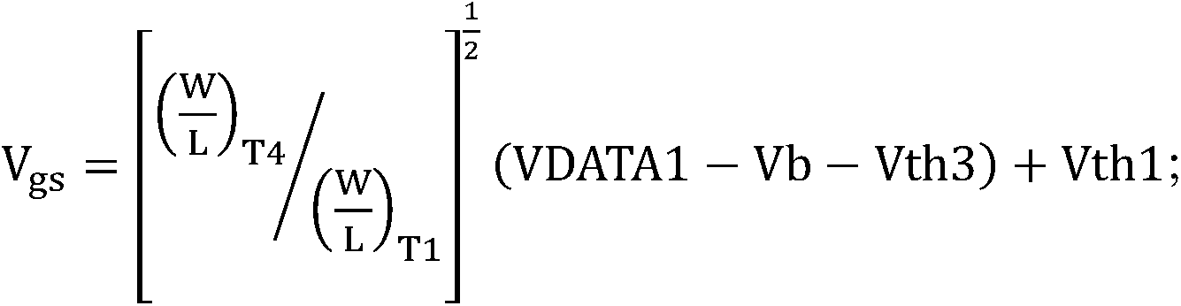 其中,Vgs为所述第一薄膜晶体管的栅源极电压,Vb为所述第二参考电压信号提供的第二参考电压,为所述第四薄膜晶体管的沟道的宽度长度比,
 为所述第一薄膜晶体管的沟道的宽度长度比,VDATA1为所述数据信号提供的显示数据信号高电位,Vth3为所述第三薄膜晶体管的阈值电压,Vth1为所述第一薄膜晶体管的阈值电压。
- 根据权利要求12所述的OLED显示装置,其中,所述第二参考电压信号提供的第二参考电压Vb满足如下公式:Vb<VDATA1-Vth3;其中,VDATA1为所述数据信号提供的显示数据信号高电位,Vth3为所述第三薄膜晶体管的阈值电压。
- 根据权利要求12所述的OLED显示装置,其中,所述第一薄膜晶体管、第二薄膜晶体管、第三薄膜晶体管、第四薄膜晶体管均为低温多晶硅薄膜晶体管、氧化物半导体薄膜晶体管或非晶硅薄膜晶体管。
Priority Applications (4)
| Application Number | Priority Date | Filing Date | Title |
|---|---|---|---|
| US15/533,445 US10347658B2 (en) | 2017-03-16 | 2017-04-20 | Pixel driving circuit and OLED display device that effectively compensate for threshold voltage imposed on a driving TFT |
| KR1020197030476A KR20190129948A (ko) | 2017-03-16 | 2017-04-20 | 픽셀 구동 회로 및 oled 디스플레이 장치 |
| JP2019550839A JP6911276B2 (ja) | 2017-03-16 | 2017-04-20 | ピクセル駆動回路及びoledディスプレイ装置 |
| EP17900438.7A EP3598427A4 (en) | 2017-03-16 | 2017-04-20 | PIXEL DRIVING CIRCUIT AND OLED DISPLAY DEVICE |
Applications Claiming Priority (2)
| Application Number | Priority Date | Filing Date | Title |
|---|---|---|---|
| CN201710156977.6 | 2017-03-16 | ||
| CN201710156977.6A CN106782340B (zh) | 2017-03-16 | 2017-03-16 | 一种像素驱动电路及oled显示装置 |
Publications (1)
| Publication Number | Publication Date |
|---|---|
| WO2018166037A1 true WO2018166037A1 (zh) | 2018-09-20 |
Family
ID=58966921
Family Applications (1)
| Application Number | Title | Priority Date | Filing Date |
|---|---|---|---|
| PCT/CN2017/081248 Ceased WO2018166037A1 (zh) | 2017-03-16 | 2017-04-20 | 一种像素驱动电路及oled显示装置 |
Country Status (6)
| Country | Link |
|---|---|
| US (1) | US10347658B2 (zh) |
| EP (1) | EP3598427A4 (zh) |
| JP (1) | JP6911276B2 (zh) |
| KR (1) | KR20190129948A (zh) |
| CN (1) | CN106782340B (zh) |
| WO (1) | WO2018166037A1 (zh) |
Families Citing this family (10)
| Publication number | Priority date | Publication date | Assignee | Title |
|---|---|---|---|---|
| CN107393466B (zh) * | 2017-08-14 | 2019-01-15 | 深圳市华星光电半导体显示技术有限公司 | 耗尽型tft的oled外部补偿电路 |
| CN107507568B (zh) | 2017-08-24 | 2019-08-13 | 深圳市华星光电半导体显示技术有限公司 | 一种oled像素电路及减缓oled器件老化的方法 |
| CN110060627B (zh) * | 2019-04-08 | 2020-11-10 | 深圳市华星光电半导体显示技术有限公司 | 像素驱动电路及显示面板 |
| CN111833817B (zh) * | 2019-04-22 | 2021-10-08 | 成都辰显光电有限公司 | 像素驱动电路、驱动方法及显示面板 |
| CN110706599B (zh) * | 2019-10-25 | 2022-01-25 | Tcl华星光电技术有限公司 | 显示面板及显示装置 |
| CN111063305A (zh) * | 2020-01-07 | 2020-04-24 | 深圳市华星光电半导体显示技术有限公司 | 像素电路、显示面板及像素电路基准电压的补偿方法 |
| CN112289266B (zh) * | 2020-10-30 | 2021-11-16 | 维沃移动通信有限公司 | 像素补偿电路、显示装置和像素补偿方法 |
| US12014683B2 (en) | 2021-04-26 | 2024-06-18 | Chengdu Boe Optoelectronics Technology Co., Ltd. | Pixel circuit, pixel driving method and display device |
| TWI826107B (zh) * | 2022-11-09 | 2023-12-11 | 友達光電股份有限公司 | 畫素電路及其驅動方法 |
| CN118379961B (zh) * | 2024-05-24 | 2024-10-15 | 国鲸合创(青岛)科技有限公司 | 主动式有机发光显示外部补偿电路及方法 |
Citations (7)
| Publication number | Priority date | Publication date | Assignee | Title |
|---|---|---|---|---|
| CN101271663A (zh) * | 2006-09-26 | 2008-09-24 | 卡西欧计算机株式会社 | 显示驱动装置及其驱动方法、显示装置及其驱动方法 |
| CN101421772A (zh) * | 2006-09-25 | 2009-04-29 | 卡西欧计算机株式会社 | 显示驱动装置和用于驱动显示驱动装置的方法以及显示装置和用于驱动显示装置的方法 |
| CN101542573A (zh) * | 2007-03-30 | 2009-09-23 | 卡西欧计算机株式会社 | 显示驱动设备、显示设备及其驱动方法 |
| US20110096061A1 (en) * | 2009-10-26 | 2011-04-28 | Industrial Technology Research Institute | Driving method and pixel driving circuit for led display panel |
| CN104680982A (zh) * | 2015-03-27 | 2015-06-03 | 深圳市华星光电技术有限公司 | Amoled像素驱动电路及像素驱动方法 |
| CN104835453A (zh) * | 2015-05-28 | 2015-08-12 | 京东方科技集团股份有限公司 | 一种像素电路、驱动方法及显示装置 |
| CN106205495A (zh) * | 2016-09-09 | 2016-12-07 | 深圳市华星光电技术有限公司 | Amoled像素驱动电路及像素驱动方法 |
Family Cites Families (10)
| Publication number | Priority date | Publication date | Assignee | Title |
|---|---|---|---|---|
| JP2004361753A (ja) * | 2003-06-05 | 2004-12-24 | Chi Mei Electronics Corp | 画像表示装置 |
| JP4747552B2 (ja) * | 2004-10-19 | 2011-08-17 | セイコーエプソン株式会社 | 電気光学装置、電子機器および方法 |
| EP2383721B1 (en) * | 2004-11-16 | 2015-04-08 | Ignis Innovation Inc. | System and Driving Method for Active Matrix Light Emitting Device Display |
| CA2495726A1 (en) * | 2005-01-28 | 2006-07-28 | Ignis Innovation Inc. | Locally referenced voltage programmed pixel for amoled displays |
| TWI424408B (zh) * | 2005-08-12 | 2014-01-21 | 半導體能源研究所股份有限公司 | 半導體裝置,和安裝有該半導體裝置的顯示裝置和電子裝置 |
| KR101809293B1 (ko) * | 2010-09-06 | 2017-12-14 | 가부시키가이샤 제이올레드 | 표시 장치 및 그 제어 방법 |
| KR101985933B1 (ko) * | 2011-11-15 | 2019-10-01 | 엘지디스플레이 주식회사 | 유기발광다이오드 표시장치 |
| US9697767B2 (en) * | 2013-07-08 | 2017-07-04 | Boe Technology Group Co., Ltd. | LED pixel unit circuit, driving method thereof, and display panel |
| US9231063B2 (en) * | 2014-02-24 | 2016-01-05 | International Business Machines Corporation | Boron rich nitride cap for total ionizing dose mitigation in SOI devices |
| CN104167177A (zh) * | 2014-08-15 | 2014-11-26 | 合肥鑫晟光电科技有限公司 | 像素电路、有机电致发光显示面板及显示装置 |
-
2017
- 2017-03-16 CN CN201710156977.6A patent/CN106782340B/zh active Active
- 2017-04-20 KR KR1020197030476A patent/KR20190129948A/ko not_active Ceased
- 2017-04-20 WO PCT/CN2017/081248 patent/WO2018166037A1/zh not_active Ceased
- 2017-04-20 JP JP2019550839A patent/JP6911276B2/ja active Active
- 2017-04-20 EP EP17900438.7A patent/EP3598427A4/en not_active Withdrawn
- 2017-04-20 US US15/533,445 patent/US10347658B2/en active Active
Patent Citations (7)
| Publication number | Priority date | Publication date | Assignee | Title |
|---|---|---|---|---|
| CN101421772A (zh) * | 2006-09-25 | 2009-04-29 | 卡西欧计算机株式会社 | 显示驱动装置和用于驱动显示驱动装置的方法以及显示装置和用于驱动显示装置的方法 |
| CN101271663A (zh) * | 2006-09-26 | 2008-09-24 | 卡西欧计算机株式会社 | 显示驱动装置及其驱动方法、显示装置及其驱动方法 |
| CN101542573A (zh) * | 2007-03-30 | 2009-09-23 | 卡西欧计算机株式会社 | 显示驱动设备、显示设备及其驱动方法 |
| US20110096061A1 (en) * | 2009-10-26 | 2011-04-28 | Industrial Technology Research Institute | Driving method and pixel driving circuit for led display panel |
| CN104680982A (zh) * | 2015-03-27 | 2015-06-03 | 深圳市华星光电技术有限公司 | Amoled像素驱动电路及像素驱动方法 |
| CN104835453A (zh) * | 2015-05-28 | 2015-08-12 | 京东方科技集团股份有限公司 | 一种像素电路、驱动方法及显示装置 |
| CN106205495A (zh) * | 2016-09-09 | 2016-12-07 | 深圳市华星光电技术有限公司 | Amoled像素驱动电路及像素驱动方法 |
Non-Patent Citations (1)
| Title |
|---|
| See also references of EP3598427A4 * |
Also Published As
| Publication number | Publication date |
|---|---|
| CN106782340A (zh) | 2017-05-31 |
| CN106782340B (zh) | 2018-09-07 |
| KR20190129948A (ko) | 2019-11-20 |
| JP2020514821A (ja) | 2020-05-21 |
| EP3598427A1 (en) | 2020-01-22 |
| JP6911276B2 (ja) | 2021-07-28 |
| EP3598427A4 (en) | 2020-11-25 |
| US20180269232A1 (en) | 2018-09-20 |
| US10347658B2 (en) | 2019-07-09 |
Similar Documents
| Publication | Publication Date | Title |
|---|---|---|
| KR102176454B1 (ko) | Amoled 픽셀 구동 회로 및 구동 방법 | |
| CN106782340B (zh) | 一种像素驱动电路及oled显示装置 | |
| CN110036435B (zh) | 像素电路、主动矩阵有机发光二极管显示面板、显示设备和补偿驱动晶体管阈值电压的方法 | |
| US10354592B2 (en) | AMOLED pixel driver circuit | |
| US10332451B2 (en) | AMOLED pixel driver circuit and pixel driving method | |
| CN106297662B (zh) | Amoled像素驱动电路及驱动方法 | |
| WO2023005621A1 (zh) | 像素电路及其驱动方法、显示面板 | |
| WO2016119304A1 (zh) | Amoled像素驱动电路及像素驱动方法 | |
| WO2018045659A1 (zh) | Amoled像素驱动电路及像素驱动方法 | |
| WO2017020360A1 (zh) | Amoled像素驱动电路及像素驱动方法 | |
| WO2016155053A1 (zh) | Amoled像素驱动电路及像素驱动方法 | |
| WO2016145693A1 (zh) | Amoled像素驱动电路及像素驱动方法 | |
| WO2018036169A1 (zh) | 像素电路、显示面板、显示设备及驱动方法 | |
| WO2017117940A1 (zh) | 像素驱动电路、像素驱动方法、显示面板和显示装置 | |
| WO2016155087A1 (zh) | Amoled像素驱动电路及像素驱动方法 | |
| WO2019033487A1 (zh) | 用于oled显示设备的像素驱动电路及oled显示设备 | |
| WO2018072298A1 (zh) | Amoled像素驱动电路及驱动方法 | |
| WO2016123855A1 (zh) | Amoled像素驱动电路及像素驱动方法 | |
| WO2016150232A1 (zh) | 像素电路及其驱动方法、显示装置 | |
| WO2019090907A1 (zh) | 一种像素驱动电路及有机发光二极管显示装置 | |
| CN108777131B (zh) | Amoled像素驱动电路及驱动方法 | |
| WO2016119305A1 (zh) | Amoled像素驱动电路及像素驱动方法 | |
| US10475385B2 (en) | AMOLED pixel driving circuit and driving method capable of ensuring uniform brightness of the organic light emitting diode and improving the display effect of the pictures | |
| WO2018149008A1 (zh) | Amoled像素驱动电路及amoled像素驱动方法 | |
| WO2019165650A1 (zh) | Amoled像素驱动电路及驱动方法 |
Legal Events
| Date | Code | Title | Description |
|---|---|---|---|
| WWE | Wipo information: entry into national phase |
Ref document number: 15533445 Country of ref document: US |
|
| 121 | Ep: the epo has been informed by wipo that ep was designated in this application |
Ref document number: 17900438 Country of ref document: EP Kind code of ref document: A1 |
|
| ENP | Entry into the national phase |
Ref document number: 2019550839 Country of ref document: JP Kind code of ref document: A |
|
| NENP | Non-entry into the national phase |
Ref country code: DE |
|
| ENP | Entry into the national phase |
Ref document number: 20197030476 Country of ref document: KR Kind code of ref document: A |
|
| ENP | Entry into the national phase |
Ref document number: 2017900438 Country of ref document: EP Effective date: 20191016 |