WO2018168308A1 - 検体検出システム - Google Patents
検体検出システム Download PDFInfo
- Publication number
- WO2018168308A1 WO2018168308A1 PCT/JP2018/005166 JP2018005166W WO2018168308A1 WO 2018168308 A1 WO2018168308 A1 WO 2018168308A1 JP 2018005166 W JP2018005166 W JP 2018005166W WO 2018168308 A1 WO2018168308 A1 WO 2018168308A1
- Authority
- WO
- WIPO (PCT)
- Prior art keywords
- temperature
- sensor chip
- temperature control
- liquid
- sensor
- Prior art date
- Legal status (The legal status is an assumption and is not a legal conclusion. Google has not performed a legal analysis and makes no representation as to the accuracy of the status listed.)
- Ceased
Links
Images






Classifications
-
- G—PHYSICS
- G01—MEASURING; TESTING
- G01N—INVESTIGATING OR ANALYSING MATERIALS BY DETERMINING THEIR CHEMICAL OR PHYSICAL PROPERTIES
- G01N33/00—Investigating or analysing materials by specific methods not covered by groups G01N1/00 - G01N31/00
- G01N33/48—Biological material, e.g. blood, urine; Haemocytometers
- G01N33/50—Chemical analysis of biological material, e.g. blood, urine; Testing involving biospecific ligand binding methods; Immunological testing
- G01N33/53—Immunoassay; Biospecific binding assay; Materials therefor
- G01N33/543—Immunoassay; Biospecific binding assay; Materials therefor with an insoluble carrier for immobilising immunochemicals
-
- G—PHYSICS
- G01—MEASURING; TESTING
- G01N—INVESTIGATING OR ANALYSING MATERIALS BY DETERMINING THEIR CHEMICAL OR PHYSICAL PROPERTIES
- G01N21/00—Investigating or analysing materials by the use of optical means, i.e. using sub-millimetre waves, infrared, visible or ultraviolet light
- G01N21/62—Systems in which the material investigated is excited whereby it emits light or causes a change in wavelength of the incident light
- G01N21/63—Systems in which the material investigated is excited whereby it emits light or causes a change in wavelength of the incident light optically excited
- G01N21/64—Fluorescence; Phosphorescence
- G01N21/6428—Measuring fluorescence of fluorescent products of reactions or of fluorochrome labelled reactive substances, e.g. measuring quenching effects, using measuring "optrodes"
-
- B—PERFORMING OPERATIONS; TRANSPORTING
- B01—PHYSICAL OR CHEMICAL PROCESSES OR APPARATUS IN GENERAL
- B01L—CHEMICAL OR PHYSICAL LABORATORY APPARATUS FOR GENERAL USE
- B01L3/00—Containers or dishes for laboratory use, e.g. laboratory glassware; Droppers
- B01L3/50—Containers for the purpose of retaining a material to be analysed, e.g. test tubes
- B01L3/502—Containers for the purpose of retaining a material to be analysed, e.g. test tubes with fluid transport, e.g. in multi-compartment structures
- B01L3/5027—Containers for the purpose of retaining a material to be analysed, e.g. test tubes with fluid transport, e.g. in multi-compartment structures by integrated microfluidic structures, i.e. dimensions of channels and chambers are such that surface tension forces are important, e.g. lab-on-a-chip
-
- B—PERFORMING OPERATIONS; TRANSPORTING
- B01—PHYSICAL OR CHEMICAL PROCESSES OR APPARATUS IN GENERAL
- B01L—CHEMICAL OR PHYSICAL LABORATORY APPARATUS FOR GENERAL USE
- B01L7/00—Heating or cooling apparatus; Heat insulating devices
-
- G—PHYSICS
- G01—MEASURING; TESTING
- G01N—INVESTIGATING OR ANALYSING MATERIALS BY DETERMINING THEIR CHEMICAL OR PHYSICAL PROPERTIES
- G01N1/00—Sampling; Preparing specimens for investigation
- G01N1/28—Preparing specimens for investigation including physical details of (bio-)chemical methods covered elsewhere, e.g. G01N33/50, C12Q
- G01N1/42—Low-temperature sample treatment, e.g. cryofixation
-
- G—PHYSICS
- G01—MEASURING; TESTING
- G01N—INVESTIGATING OR ANALYSING MATERIALS BY DETERMINING THEIR CHEMICAL OR PHYSICAL PROPERTIES
- G01N1/00—Sampling; Preparing specimens for investigation
- G01N1/28—Preparing specimens for investigation including physical details of (bio-)chemical methods covered elsewhere, e.g. G01N33/50, C12Q
- G01N1/44—Sample treatment involving radiation, e.g. heat
-
- G—PHYSICS
- G01—MEASURING; TESTING
- G01N—INVESTIGATING OR ANALYSING MATERIALS BY DETERMINING THEIR CHEMICAL OR PHYSICAL PROPERTIES
- G01N21/00—Investigating or analysing materials by the use of optical means, i.e. using sub-millimetre waves, infrared, visible or ultraviolet light
- G01N21/01—Arrangements or apparatus for facilitating the optical investigation
- G01N21/03—Cuvette constructions
- G01N21/0332—Cuvette constructions with temperature control
-
- G—PHYSICS
- G01—MEASURING; TESTING
- G01N—INVESTIGATING OR ANALYSING MATERIALS BY DETERMINING THEIR CHEMICAL OR PHYSICAL PROPERTIES
- G01N21/00—Investigating or analysing materials by the use of optical means, i.e. using sub-millimetre waves, infrared, visible or ultraviolet light
- G01N21/62—Systems in which the material investigated is excited whereby it emits light or causes a change in wavelength of the incident light
- G01N21/63—Systems in which the material investigated is excited whereby it emits light or causes a change in wavelength of the incident light optically excited
- G01N21/64—Fluorescence; Phosphorescence
- G01N21/645—Specially adapted constructive features of fluorimeters
- G01N21/648—Specially adapted constructive features of fluorimeters using evanescent coupling or surface plasmon coupling for the excitation of fluorescence
-
- G—PHYSICS
- G01—MEASURING; TESTING
- G01N—INVESTIGATING OR ANALYSING MATERIALS BY DETERMINING THEIR CHEMICAL OR PHYSICAL PROPERTIES
- G01N33/00—Investigating or analysing materials by specific methods not covered by groups G01N1/00 - G01N31/00
- G01N33/48—Biological material, e.g. blood, urine; Haemocytometers
- G01N33/50—Chemical analysis of biological material, e.g. blood, urine; Testing involving biospecific ligand binding methods; Immunological testing
- G01N33/53—Immunoassay; Biospecific binding assay; Materials therefor
- G01N33/543—Immunoassay; Biospecific binding assay; Materials therefor with an insoluble carrier for immobilising immunochemicals
- G01N33/54366—Apparatus specially adapted for solid-phase testing
- G01N33/54373—Apparatus specially adapted for solid-phase testing involving physiochemical end-point determination, e.g. wave-guides, FETS, gratings
-
- G—PHYSICS
- G01—MEASURING; TESTING
- G01N—INVESTIGATING OR ANALYSING MATERIALS BY DETERMINING THEIR CHEMICAL OR PHYSICAL PROPERTIES
- G01N35/00—Automatic analysis not limited to methods or materials provided for in any single one of groups G01N1/00 - G01N33/00; Handling materials therefor
-
- B—PERFORMING OPERATIONS; TRANSPORTING
- B01—PHYSICAL OR CHEMICAL PROCESSES OR APPARATUS IN GENERAL
- B01L—CHEMICAL OR PHYSICAL LABORATORY APPARATUS FOR GENERAL USE
- B01L2200/00—Solutions for specific problems relating to chemical or physical laboratory apparatus
- B01L2200/14—Process control and prevention of errors
- B01L2200/143—Quality control, feedback systems
- B01L2200/147—Employing temperature sensors
-
- B—PERFORMING OPERATIONS; TRANSPORTING
- B01—PHYSICAL OR CHEMICAL PROCESSES OR APPARATUS IN GENERAL
- B01L—CHEMICAL OR PHYSICAL LABORATORY APPARATUS FOR GENERAL USE
- B01L2300/00—Additional constructional details
- B01L2300/08—Geometry, shape and general structure
- B01L2300/0861—Configuration of multiple channels and/or chambers in a single devices
- B01L2300/0877—Flow chambers
-
- B—PERFORMING OPERATIONS; TRANSPORTING
- B01—PHYSICAL OR CHEMICAL PROCESSES OR APPARATUS IN GENERAL
- B01L—CHEMICAL OR PHYSICAL LABORATORY APPARATUS FOR GENERAL USE
- B01L2300/00—Additional constructional details
- B01L2300/16—Surface properties and coatings
- B01L2300/168—Specific optical properties, e.g. reflective coatings
-
- G—PHYSICS
- G01—MEASURING; TESTING
- G01N—INVESTIGATING OR ANALYSING MATERIALS BY DETERMINING THEIR CHEMICAL OR PHYSICAL PROPERTIES
- G01N21/00—Investigating or analysing materials by the use of optical means, i.e. using sub-millimetre waves, infrared, visible or ultraviolet light
- G01N21/62—Systems in which the material investigated is excited whereby it emits light or causes a change in wavelength of the incident light
- G01N21/63—Systems in which the material investigated is excited whereby it emits light or causes a change in wavelength of the incident light optically excited
- G01N21/64—Fluorescence; Phosphorescence
- G01N21/6428—Measuring fluorescence of fluorescent products of reactions or of fluorochrome labelled reactive substances, e.g. measuring quenching effects, using measuring "optrodes"
- G01N2021/6439—Measuring fluorescence of fluorescent products of reactions or of fluorochrome labelled reactive substances, e.g. measuring quenching effects, using measuring "optrodes" with indicators, stains, dyes, tags, labels, marks
Definitions
- the present invention relates to a sample detection system that detects a measurement target substance contained in a sensor chip, and more specifically, a sample capable of strictly controlling the temperature of a reaction part of a sensor chip to which the measurement target substance is immobilized. Relates to the detection system.
- specimen detection methods when detecting a very small substance, various specimen detection methods have been proposed that can detect such a substance by applying a physical phenomenon of the substance.
- a specimen detection method for example, by using an antigen-antibody reaction between an antigen, which is a measurement target substance contained in a sample solution, and an antibody or antigen labeled with a labeling substance, the presence or absence of the measurement target substance or its Immunoassay methods (immunoassays) for measuring amounts are known.
- the immunoassay examples include an enzyme immunoassay (EIA) using an enzyme as a labeling substance, and a fluorescence immunoassay (FIA) using a fluorescent substance as a labeling substance.
- EIA enzyme immunoassay
- FIA fluorescence immunoassay
- a specimen detection device using a fluorescence immunoassay method a phenomenon in which high light output is obtained by resonating electrons and light in a fine region such as a nanometer level (SPR: Surface Plasmon Resonance)
- SPR apparatus surface plasmon resonance apparatus that detects minute alanite in a living body is used.
- SPFS device based on the principle of surface plasmon excitation enhanced fluorescence spectroscopy (SPFS) using surface plasmon resonance (SPR) phenomenon, analyte detection can be performed with higher accuracy than SPR equipment.
- SPFS device The surface plasmon excitation enhanced fluorescence spectrometer (hereinafter also referred to as “SPFS device”) is one of such specimen detection devices.
- surface plasmon excitation enhanced fluorescence spectroscopy SPFS
- surface plasmon light is applied to the surface of the metal film under the condition that excitation light such as laser light emitted from a light source attenuates total reflection (ATR) on the surface of the metal film.
- excitation light such as laser light emitted from a light source attenuates total reflection (ATR) on the surface of the metal film.
- ATR total reflection
- a sensor chip including a dielectric member, a metal film adjacent to the upper surface of the dielectric member, and a liquid holding member disposed on the upper surface of the metal film is used.
- a reaction part having a ligand for capturing an analyte is provided on a metal film.
- the analyte By supplying a sample solution containing the analyte to the liquid holding member, the analyte is captured by the ligand (primary reaction). In this state, a liquid (labeling liquid) containing a secondary antibody labeled with a fluorescent substance is introduced into the liquid holding member. In the solution holding member, the analyte captured by the ligand is labeled with a fluorescent substance by an antigen-antibody reaction (secondary reaction).
- the fluorescent material is excited by the surface plasmon light generated on the surface of the metal film, and fluorescence is generated from the fluorescent material. By detecting this fluorescence, the presence or absence of the analyte and the amount thereof can be measured.
- the reactivity of immune reactions such as primary reactions and secondary reactions generally varies depending on the temperature of the reaction field.
- specimen testing using an SPFS apparatus is performed with the SPFS apparatus installed at room temperature, but it is required to control the reaction field to a predetermined temperature from the viewpoint of promoting an immune reaction and stabilizing reaction efficiency. ing.
- Patent Document 1 Japanese Patent Application Laid-Open No. 2012-215465
- a first temperature sensor that measures the temperature around the sensor chip and a second temperature that measures the temperature of the contact portion between the sensor chip and the temperature control unit. It has been proposed to adjust the temperature of a sensor chip by using a sensor to perform feedback control of a temperature adjustment unit that contacts the sensor chip and adjusts the temperature of the sensor chip.
- the temperature of the heat transfer body surface of the temperature control part that contacts the sensor chip is obtained.
- the temperature of the heat transfer body surface of the temperature adjustment unit that is in contact with the sensor chip measured by the second temperature sensor is the target value. The temperature of the sensor chip is adjusted.
- the temperature of the reaction part of the sensor chip is controlled to be constant by setting the target value high.
- a temperature gradient or temperature unevenness occurs in a portion close to and far from the temperature control portion (or a portion that easily radiates heat).
- liquid such as sample liquid and cleaning solution is sequentially introduced into the sensor chip within the sample detection device, so the temperature of the reaction part of the sensor chip is introduced. It is affected by the temperature of the liquid.
- the present invention provides a sample detection system that can suppress temperature gradients and temperature unevenness in a sensor chip, and can control the temperature of the reaction section with higher accuracy without depending on the environmental temperature where the sample detection device is installed.
- the purpose is to do.
- a sample detection system for detecting an analyte using a sensor chip having a reaction field for capturing an analyte inside A contact temperature control unit disposed in contact with the sensor chip; A non-contact temperature control unit disposed in a non-contact manner with respect to the sensor chip, The contact-type temperature control unit includes first temperature control means, and a first temperature sensor that measures a temperature between the first temperature control means and the sensor chip, and an output value of the first temperature sensor; The first temperature control means is feedback-controlled based on a predetermined first temperature control means target temperature, The non-contact temperature control unit includes a second temperature control unit, and a second temperature sensor that measures a temperature between the second temperature control unit and the sensor chip, and an output value of the second temperature sensor. And the second temperature control means are feedback-controlled based on the predetermined second temperature control
- non-contact temperature control means such as hot and cold air
- the temperature of the reaction part can be controlled with high accuracy.
- the temperature of the environment in which the sample detection device is installed is measured, and the temperature target value of the non-contact temperature control means such as hot and cold air is controlled based on this environmental temperature. Regardless of the environmental temperature, the temperature of the reaction section can be controlled with high accuracy.
- FIG. 1 is a schematic diagram for explaining a configuration of a surface plasmon excitation enhanced fluorescence spectrometer (SPFS apparatus) according to an embodiment of the present invention.
- FIG. 2 is a flowchart illustrating an example of an operation procedure of the SPFS apparatus according to the present embodiment.
- FIG. 3 is a graph for explaining the relationship between the elapsed time from the start of specimen detection and the second temperature adjustment means target temperature T2.
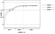
- FIG. 4 is a graph showing the relationship between the elapsed time and the reaction field temperature when the temperature of the sensor chip is controlled using the SPFS apparatus in the present embodiment.
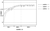
- FIG. 5 is a graph showing the relationship between the elapsed time and the reaction field temperature when the temperature of the sensor chip is adjusted as Comparative Example 1.
- FIG. 1 is a schematic diagram for explaining a configuration of a surface plasmon excitation enhanced fluorescence spectrometer (SPFS apparatus) according to an embodiment of the present invention.
- FIG. 2 is a flowchart illustrating an example of an
- FIG. 6 is a graph showing the relationship between the elapsed time and the reaction field temperature when the temperature of the sensor chip is adjusted as Comparative Example 2.
- FIG. 7 is a graph showing the relationship between the elapsed time and the reaction field temperature when the temperature of the sensor chip is adjusted as Comparative Example 3.
- FIG. 8 is a schematic view showing a modification of the contact temperature control unit.
- FIG. 9 is a schematic diagram showing a modification of the non-contact temperature control unit.
- FIG. 10 is a schematic diagram illustrating a modified example of the sensor chip.
- FIG. 1 is a schematic diagram for explaining a configuration of a surface plasmon excitation enhanced fluorescence spectrometer (SPFS apparatus) according to an embodiment of the present invention.
- SPFS apparatus surface plasmon excitation enhanced fluorescence spectrometer
- the SPFS apparatus 10 includes an excitation light irradiation unit 20, a fluorescence detection unit 30, a liquid feeding unit 40, a transport unit 50, a contact temperature control unit 60, a non-contact temperature control unit 70, and a control unit 80. Is housed in the housing 12.
- the SPFS device 10 is used in a state where the sensor chip 100 is mounted on the chip holder 54 of the transport unit 50.
- the sensor chip 100 is fixed on the dielectric member 102 having the incident surface 102a, the film formation surface 102b, and the emission surface 102c, the metal film 104 formed on the film formation surface 102b, and the film formation surface 102b or the metal film 104.
- a flow path forming member 106 that is a liquid holding member, and a liquid storage member 108 that stores a sample liquid, a labeling liquid, a cleaning liquid, and the like.
- the sensor chip 100 is replaced for each specimen test.
- the sensor chip 100 is preferably a structure having a length of several millimeters to several centimeters on each side, but is a smaller structure or a larger structure that is not included in the category of “chip”. It doesn't matter.
- the dielectric member 102 can be a prism made of a dielectric that is transparent to the excitation light ⁇ .
- the incident surface 102 a of the dielectric member 102 is a surface on which the excitation light ⁇ irradiated from the excitation light irradiation unit 20 is incident on the inside of the dielectric member 102.
- a metal film 104 is formed on the film formation surface 102b.
- the excitation light ⁇ incident on the inside of the dielectric member 102 is reflected at the interface between the metal film 104 and the film formation surface 102b of the dielectric member 102 (hereinafter referred to as “the back surface of the metal film 104” for convenience), and the emission surface.
- the excitation light ⁇ is emitted to the outside of the dielectric member 102 through 102c.
- the shape of the dielectric member 102 is not particularly limited, and the dielectric member 102 shown in FIG. 1 is a prism composed of a hexahedron having a substantially trapezoidal vertical cross-sectional shape (a truncated quadrangular pyramid shape).
- a prism having a cross-sectional shape of a triangle (a so-called triangular prism), a semicircular shape, or a semielliptical shape may be used.
- the incident surface 102 a is formed so that the excitation light ⁇ does not return to the excitation light irradiation unit 20.
- the light source of the excitation light ⁇ is, for example, a laser diode (hereinafter also referred to as “LD”)
- LD laser diode
- the angle of the incident surface 102a is set so that the excitation light ⁇ does not enter the incident surface 102a perpendicularly in the scanning range centered on the ideal enhancement angle.
- the resonance angle (and the enhancement angle in the vicinity thereof) is generally determined by the design of the sensor chip 100.
- the design elements are the refractive index of the dielectric member 102, the refractive index of the metal film 104, the film thickness of the metal film 104, the extinction coefficient of the metal film 104, the wavelength of the excitation light ⁇ , and the like.
- the resonance angle and the enhancement angle are shifted by the analyte immobilized on the metal film 104, but the amount is less than a few degrees.
- the dielectric member 102 has a considerable amount of birefringence.
- the material of the dielectric member 102 includes, for example, various inorganic materials such as glass and ceramics, natural polymers, synthetic polymers, and the like, and is excellent in chemical stability, manufacturing stability, optical transparency, and low birefringence. Is preferred.
- the material is not particularly limited as described above. In providing, for example, it is preferably formed from a resin material.
- the method for manufacturing the dielectric member 102 is not particularly limited, but injection molding using a mold is preferable from the viewpoint of manufacturing cost.
- the dielectric member 102 is formed from a resin material, for example, polyolefins such as polyethylene (PE) and polypropylene (PP), polycyclic olefins such as cyclic olefin copolymer (COC) and cyclic olefin polymer (COP), polystyrene, Polycarbonate (PC), acrylic resin, triacetyl cellulose (TAC), or the like can be used.
- PE polyethylene
- PP polypropylene
- polycyclic olefins such as cyclic olefin copolymer (COC) and cyclic olefin polymer (COP), polystyrene, Polycarbonate (PC), acrylic resin, triacetyl cellulose (TAC), or the like
- PC polycarbonate
- TAC triacetyl cellulose
- the metal film 104 is formed on the film formation surface 102 b of the dielectric member 102.
- an interaction (surface plasmon resonance) occurs between the photon of the excitation light ⁇ incident on the film formation surface 102b under the total reflection condition and the free electrons in the metal film 104, and is locally on the surface of the metal film 104. In-situ light can be generated.
- the material of the metal film 104 is not particularly limited as long as it is a metal capable of causing surface plasmon resonance.
- a metal capable of causing surface plasmon resonance.
- at least one metal selected from the group consisting of gold, silver, aluminum, copper, and platinum is used.
- Such a metal is suitable as the metal film 104 because it is stable against oxidation and has a large electric field enhancement by surface plasmon light.
- the method for forming the metal film 104 is not particularly limited, and examples thereof include sputtering, vapor deposition (resistance heating vapor deposition, electron beam vapor deposition, etc.), electrolytic plating, electroless plating, and the like. It is done.
- the sputtering method or the vapor deposition method is used because the adjustment of the metal film forming conditions is easy.
- the thickness of the metal film 104 is not particularly limited, but is preferably in the range of 5 to 500 nm, and more preferably gold, silver, copper, In the case of platinum, it is preferably in the range of 20 to 70 nm, in the case of aluminum, 10 to 50 nm, and in the case of these alloys, it is preferably in the range of 10 to 70 nm.
- the thickness of the metal film 104 is within the above range, it is preferable that surface plasmon light is easily generated.
- the size (length ⁇ width) dimensions and shape are not particularly limited.
- a ligand for capturing the analyte is immobilized on the surface of the metal film 104 that does not face the dielectric member 102 (hereinafter referred to as “the surface of the metal film 104” for convenience). Yes. By immobilizing the ligand, the analyte can be selectively detected.
- the ligand is uniformly immobilized in a predetermined region (reaction field) on the metal film 104.
- the type of the ligand is not particularly limited as long as the analyte can be captured.
- the ligand is an analyte specific antibody or fragment thereof.
- the flow path forming member 106 is disposed on the film formation surface 102 b of the dielectric member 102 or the metal film 104. Further, the flow path forming member 106 is formed with a flow path groove 110 on the surface facing the film formation surface 102 b or the metal film 104. The flow path forming member 106 is disposed so as to cover the reaction field on the metal film 104, and the flow path for feeding the sample liquid, the labeling liquid, the cleaning liquid, etc. by the flow path forming member 106 and the dielectric member 102. 112 is formed.
- the flow path forming member 106 can be bonded to the dielectric member 102 or the metal film 104 by, for example, adhesion using an adhesive or a transparent adhesive sheet, laser welding, ultrasonic welding, or pressure bonding using a clamp member. .
- the flow path forming member 106 and the dielectric member 102 or the metal film 104 are bonded to each other with the adhesive sheet in which the through hole is formed without forming the flow path groove 110, so that the through hole of the adhesive sheet is used as the flow path. It can also be used.
- the flow path forming member 106 has a first through hole 110 a formed at one end of the flow path groove 110 and a second through hole 110 b formed at the other end of the flow path groove 110.
- each of the first through hole 110a and the second through hole 110b has a substantially cylindrical shape.
- the first through hole 110a and the second through hole 110b serve as an inlet for injecting a sample liquid, a labeling liquid, a cleaning liquid, and the like into the flow path 112, and an outlet for taking out the sample liquid, the labeling liquid, the cleaning liquid, and the like. Function.
- the material of the flow path forming member 106 is not particularly limited as long as it is formed of a material that is optically transparent to at least the fluorescent ⁇ described later, but the sensor chip 100 that is inexpensive and excellent in handleability is used. In providing, for example, it is preferably formed from a resin material.
- the manufacturing method of the flow path forming member 106 is not particularly limited, but injection molding using a mold is preferable from the viewpoint of manufacturing cost.
- polyesters such as polyethylene terephthalate (PET) and polyethylene naphthalate
- polyolefins such as polyethylene (PE) and polypropylene (PP), cyclic olefin copolymer (COC)
- Polycyclic olefins such as cyclic olefin polymer (COP)
- vinyl resins such as polyvinyl chloride and polyvinylidene chloride, polystyrene, polyetheretherketone (PEEK), polysulfone (PSF), polyethersulfone (PES), polycarbonate (PC), polyamide, polyimide, acrylic resin, triacetyl cellulose (TAC), or the like
- PEEK polyetheretherketone
- PSF polysulfone
- PES polyethersulfone
- PC polycarbonate
- polyamide polyimide
- acrylic resin triacetyl cellulose
- the liquid storage member 108 has a well 108a for storing a sample liquid, a labeling liquid, a cleaning liquid, and the like.
- the liquid storage member 108 is formed integrally with the flow path forming member 106.
- a sample liquid, a labeling liquid, a cleaning liquid, and the like used for a primary reaction and a secondary reaction described later are stored, respectively.
- the shape of the well 108a is not particularly limited, and can be appropriately set according to the amount of the sample solution, labeling solution, washing solution, etc. to be stored.
- the SPFS device 10 shown in FIG. 1 only one well 108a is shown, but a plurality of wells 108a may be provided according to the number of liquids used for specimen detection.
- liquid storage member 108 and the flow path forming member 106 are integrally formed.
- the liquid storage member 108 may be configured as a separate chip from the flow path forming member 106.
- the material of the liquid storage member 108 is not particularly limited, but is preferably formed from, for example, a resin material in order to provide the sensor chip 100 that is inexpensive and excellent in handleability.
- the method for manufacturing the liquid storage member 108 is not particularly limited, but injection molding using a mold is preferable from the viewpoint of manufacturing cost.
- the liquid storage member 108 is formed of a resin material
- polyesters such as polyethylene terephthalate (PET) and polyethylene naphthalate
- polyolefins such as polyethylene (PE) and polypropylene (PP)
- COC cyclic olefin copolymer
- COP olefin polymer
- vinyl resins such as polyvinyl chloride and polyvinylidene chloride, polystyrene, polyether ether ketone (PEEK), polysulfone (PSF), polyether sulfone (PES), polycarbonate ( PC), polyamide, polyimide, acrylic resin, triacetyl cellulose (TAC), and the like
- PC polyamide
- polyimide acrylic resin
- TAC triacetyl cellulose
- the sensor chip 100 configured as described above is mounted on the chip holder 54 of the transport unit 50 of the SPFS apparatus 10, and specimen detection is performed by the SPFS apparatus 10.
- the SPFS device 10 includes the excitation light irradiation unit 20, the fluorescence detection unit 30, the liquid feeding unit 40, the transport unit 50, the contact temperature control unit 60, the non-contact temperature control unit 70, and the control.
- the part 80 is accommodated in the housing 12.
- the excitation light irradiation unit 20 irradiates the sensor chip 100 held by the chip holder 54 with the excitation light ⁇ . As will be described later, when measuring the fluorescence ⁇ , the excitation light irradiation unit 20 directs only the P wave with respect to the metal film 104 toward the incident surface 102a so that the incident angle with respect to the metal film 104 is an angle that causes surface plasmon resonance. And exit.
- the “excitation light” is light that directly or indirectly excites the fluorescent substance.
- the excitation light ⁇ is irradiated through the dielectric member 102 at an angle at which surface plasmon resonance occurs on the metal film 104, local field light that excites the fluorescent material is generated on the surface of the metal film 104. Light.
- the excitation light irradiation unit 20 includes a configuration for emitting the excitation light ⁇ toward the dielectric member 102 and a configuration for scanning the incident angle of the excitation light ⁇ with respect to the back surface of the metal film 104.
- the excitation light irradiation unit 20 includes a light source unit 21, an angle adjustment mechanism 22, and a light source control unit 23.
- the light source unit 21 irradiates collimated excitation light ⁇ having a constant wavelength and light amount so that the irradiation spot has a substantially circular shape on the back surface of the metal film 104.
- the light source unit 21 includes, for example, a light source of excitation light ⁇ , a beam shaping optical system, an APC (Automatic Power-Control) mechanism, and a temperature adjustment mechanism (all not shown).
- the type of light source is not particularly limited, and includes, for example, a laser diode (LD), a light emitting diode, a mercury lamp, and other laser light sources.
- LD laser diode
- the light emitted from the light source is converted into a beam by a lens, a mirror, a slit, or the like.
- the light emitted from the light source is not monochromatic light, the light emitted from the light source is converted into monochromatic light by a diffraction grating or the like.
- the light emitted from the light source is not linearly polarized light, the light emitted from the light source is converted into linearly polarized light by a polarizer or the like.
- the beam shaping optical system includes, for example, a collimator, a band pass filter, a linear polarization filter, a half-wave plate, a slit, and a zoom means.
- the beam shaping optical system may include all of these or only a part thereof.
- the collimator collimates the excitation light ⁇ irradiated from the light source.
- the band-pass filter turns the excitation light ⁇ irradiated from the light source into narrowband light having only the center wavelength. This is because the excitation light ⁇ from the light source has a slight wavelength distribution width.
- the linear polarization filter turns the excitation light ⁇ irradiated from the light source into completely linearly polarized light.
- the half-wave plate adjusts the polarization direction of the excitation light ⁇ so that the P-wave component is incident on the metal film 104.
- the slit and zoom means adjust the beam diameter, contour shape, and the like of the excitation light ⁇ so that the shape of the irradiation spot on the back surface of the metal film 104 is a circle having a predetermined size.
- the APC mechanism controls the light source so that the output of the light source is constant. More specifically, the APC mechanism detects the amount of light branched from the excitation light ⁇ with a photodiode (not shown) or the like. The APC mechanism controls the input energy by a regression circuit, thereby controlling the output of the light source to be constant.
- the temperature adjustment mechanism is, for example, a heater or a Peltier element.
- the wavelength and energy of the light emitted from the light source may vary depending on the temperature. For this reason, the wavelength and energy of the light emitted from the light source are controlled to be constant by keeping the temperature of the light source constant by the temperature adjusting mechanism.
- the angle adjustment mechanism 22 adjusts the incident angle of the excitation light ⁇ to the metal film 104.
- the angle adjustment mechanism 22 makes the optical axis of the excitation light ⁇ and the chip holder 54 relative to each other. Rotate.
- the angle adjusting mechanism 22 rotates the light source unit 21 around an axis (axis perpendicular to the paper surface of FIG. 1) orthogonal to the optical axis of the excitation light ⁇ .
- the position of the rotation axis is set so that the position of the irradiation spot on the metal film 104 hardly changes even when the incident angle is scanned.
- the angle at which the maximum amount of plasmon scattered light can be obtained is the enhancement angle.
- the basic incident condition of the excitation light ⁇ is determined by the material and shape of the dielectric member 102 of the sensor chip 100, the film thickness of the metal film 104, the refractive index of the sample liquid in the flow path 112, and the like.
- the optimum incident condition varies slightly depending on the type and amount of the analyte in the flow path 112, the shape error of the dielectric member 102, and the like. For this reason, it is preferable to obtain an optimal enhancement angle for each specimen test.
- the light source control unit 23 controls various devices included in the light source unit 21 to control the irradiation of the excitation light ⁇ of the light source unit 21.
- the light source control unit 23 includes, for example, a known computer or microcomputer including an arithmetic device, a control device, a storage device, an input device, and an output device.
- the fluorescence detection unit 30 detects the fluorescence ⁇ generated from the fluorescent material excited by the irradiation of the excitation light ⁇ to the metal film 104. If necessary, the fluorescence detection unit 30 also detects plasmon scattered light generated by the irradiation of the excitation light ⁇ to the metal film 104.
- the fluorescence detection unit 30 includes, for example, a light receiving unit 31, a position switching mechanism 37, and a sensor control unit 38.
- the light receiving unit 31 is disposed in the normal direction of the metal film 104 of the sensor chip 100 (z-axis direction in FIG. 1).
- the light receiving unit 31 includes a first lens 32, an optical filter 33, a second lens 34, and a light receiving sensor 35.
- the first lens 32 is, for example, a condensing lens and condenses light generated on the metal film 104.
- the second lens 34 is, for example, an imaging lens, and forms an image of the light collected by the first lens 32 on the light receiving surface of the light receiving sensor 35.
- the optical path between both lenses 32 and 34 is a substantially parallel optical path.
- the optical filter 33 is disposed between the lenses 32 and 34.
- the optical filter 33 guides only the fluorescent component to the light receiving sensor 35 and removes the excitation light component (plasmon scattered light) in order to detect the fluorescent ⁇ with high S / N.
- the optical filter 33 includes, for example, an excitation light reflection filter, a short wavelength cut filter, and a band pass filter.
- the optical filter 33 is, for example, a filter including a multilayer film that reflects a predetermined light component, but may be a colored glass filter that absorbs the predetermined light component.
- the light receiving sensor 35 detects fluorescence ⁇ .
- the light receiving sensor 35 is not particularly limited as long as it has a high sensitivity and can detect weak fluorescence ⁇ from a fluorescent substance labeled with a very small amount of analyte.
- a multiplier tube (PMT), an avalanche photodiode (APD), a low noise photodiode (PD), or the like can be used.
- the position switching mechanism 37 switches the position of the optical filter 33 on or off the optical path in the light receiving unit 31. Specifically, when the light receiving sensor 35 detects the fluorescence ⁇ , the optical filter 33 is disposed on the optical path of the light receiving unit 31, and when the light receiving sensor 35 detects plasmon scattered light, the optical filter 33 is placed on the light receiving unit 31. Place outside the optical path.
- the position switching mechanism 37 includes, for example, a rotation driving unit and a known mechanism (such as a turntable or a rack and pinion) that moves the optical filter 33 in the horizontal direction by using a rotational motion.
- the sensor control unit 38 controls detection of an output value of the light receiving sensor 35, management of sensitivity of the light receiving sensor 35 based on the detected output value, change of sensitivity of the light receiving sensor 35 for obtaining an appropriate output value, and the like.
- the sensor control unit 38 includes, for example, a known computer or microcomputer including an arithmetic device, a control device, a storage device, an input device, and an output device.
- the liquid feeding unit 40 supplies a sample liquid, a labeling liquid, a cleaning liquid, and the like into the flow path 112 of the sensor chip 100 mounted on the chip holder 54.
- the liquid feeding unit 40 includes a syringe pump 41, a pipette nozzle 46, a pipette tip 45, and a liquid feeding pump drive mechanism 44.
- the liquid feeding unit 40 is used with a pipette tip 45 attached to the tip of the pipette nozzle 46. If the pipette tip 45 is replaceable, the pipette tip 45 need not be washed, and contamination of impurities can be prevented.
- the syringe pump 41 includes a syringe 42 and a plunger 43 that can reciprocate inside the syringe 42. By the reciprocating motion of the plunger 43, the liquid is sucked and discharged quantitatively.
- the liquid feed pump driving mechanism 44 includes a driving device for the syringe pump 41 and a moving device for the pipette nozzle 46 to which the pipette tip 45 is attached.
- the drive device of the syringe pump 41 is a device for reciprocating the plunger 43, and includes, for example, a stepping motor.
- a drive device including a stepping motor is preferable from the viewpoint of managing the remaining liquid amount of the sensor chip 100 because it can manage the liquid feeding amount and the liquid feeding speed of the syringe pump 41.
- the moving device of the pipette nozzle 46 freely moves the pipette nozzle 46 in two directions, that is, an axial direction (for example, a vertical direction) of the pipette nozzle 46 and a direction crossing the axial direction (for example, a horizontal direction).
- the moving device of the pipette nozzle 46 is constituted by, for example, a robot arm, a two-axis stage, or a turntable that can move up and down.
- the liquid feeding unit 40 is provided at the tip of the pipette tip 45. It is preferable to further have a mechanism for detecting the position.
- the liquid feeding unit 40 sucks various liquids from the liquid storage member 108 and supplies them into the flow path 112 of the sensor chip 100. At this time, by moving the plunger 43, the liquid reciprocates in the flow path 112 of the sensor chip 100, and the liquid in the flow path 112 is stirred. As a result, it is possible to make the liquid concentration uniform and promote the reaction (for example, antigen-antibody reaction) in the flow path 112.
- the inlet (first through hole 110a) of the sensor chip 100 is protected by the multilayer film 111 and the first through hole when the pipette chip 45 penetrates the multilayer film.
- the sensor chip 100 and the pipette chip 45 are preferably configured so that the 110a can be sealed.
- the liquid in the flow path 112 is again sucked by the syringe pump 41 and discharged to the liquid storage member 108 and the like.
- reaction with various liquids, washing, and the like can be performed, and the analyte labeled with the fluorescent substance can be immobilized in the reaction field in the channel 112.
- the transport unit 50 transports and fixes the sensor chip 100 mounted on the chip holder 54 to the liquid feeding position or the measurement position by the user.
- the “liquid feeding position” is a position where the liquid feeding unit 40 supplies the liquid into the flow path 112 of the sensor chip 100 or removes the liquid in the flow path 112.
- the “measurement position” is a position where the excitation light irradiation unit 20 irradiates the sensor chip 100 with the excitation light ⁇ , and the fluorescence detection unit 30 detects the fluorescence ⁇ generated therewith.
- the transport unit 50 is also used to change the distance between the sensor chip 100 and the light source unit 21 of the excitation light irradiation unit 20 in a position detection and position adjustment process described later.
- the transfer unit 50 includes a transfer stage 52 and a chip holder 54.
- the chip holder 54 is fixed to the transfer stage 52 and holds the sensor chip 100 in a detachable manner.
- the shape of the chip holder 54 is not particularly limited as long as it can hold the sensor chip 100 and does not obstruct the optical paths of the excitation light ⁇ and the fluorescence ⁇ .
- the chip holder 54 is provided with an opening through which excitation light ⁇ and fluorescence ⁇ pass.
- the transfer stage 52 is configured to be able to move the chip holder 54 in one direction (x-axis direction in FIG. 1) and in the opposite direction.
- the transport stage 52 is driven by, for example, a stepping motor.
- the contact temperature control unit 60 includes a first temperature control unit 61 disposed in contact with the sensor chip 100, and a first temperature sensor disposed between the first temperature control unit 61 and the reaction field of the sensor chip 100. 62.
- the first temperature adjusting means 61 is controlled by the control unit 80 described later so as to reach a predetermined temperature.
- the first temperature adjustment means 61 includes a temperature adjustment element 61a and a heat transfer member 61b.
- the temperature control element 61a may be a heating element or a cooling element.
- the temperature control element 61a is not particularly limited, and for example, an electric resistance element, an infrared heater such as a cartridge heater, a rubber heater, or a ceramic heater, a Peltier element, or the like can be used.
- the heat transfer member 61b has a shape that does not block the optical paths of the excitation light ⁇ and the fluorescence ⁇ , and transfers heat from the temperature adjustment element 61a to the sensor chip 100.
- the material of such a heat transfer member 61b is not particularly limited, but for example, a metal having high thermal conductivity such as copper or aluminum can be used.
- the heat transfer member 61b is in contact with the lower surface 102d of the dielectric member 102 and is also in contact with the well 108a of the liquid storage member 108. Accordingly, the temperature of the liquid stored in the well 108a of the liquid storage member 108 can be adjusted simultaneously with the temperature adjustment of the reaction field of the sensor chip 100. For this reason, the temperature of the liquid introduced into the flow path 112 of the sensor chip 100 can be controlled in advance, and the change in the temperature of the reaction field accompanying the liquid introduction into the flow path 112 can be suppressed.
- the first temperature sensor 62 is not particularly limited as long as it can transmit a signal (output value) corresponding to the measured temperature to the control unit 80 described later.
- the thermistor, thermocouple, etc. Can be used.
- the first temperature sensor 62 only needs to be at a position where the temperature between the first temperature adjusting means 61 and the sensor chip 100 can be measured, and can be arranged at a position closer to the sensor chip 100 having the reaction field. preferable. For example, it can be provided at a position in contact with any surface of the dielectric member 102 on the heat transfer member 61 b or inside the heat transfer member 61 b close to the dielectric member 12.
- the non-contact type temperature control unit 70 includes a second temperature control unit 71 disposed away from the sensor chip 100, and a second temperature sensor 72 disposed between the second temperature control unit 71 and the sensor chip 100. And air blowing means 73 for sending the air heated or cooled by the second temperature adjusting means 71 to the sensor chip 100.
- the non-contact temperature control unit 70 is provided so that the temperature of the sensor chip 100 can be controlled in a state where the sensor chip 100 is in the liquid feeding position.
- the second temperature adjusting means 71 is controlled by the control unit 80 described later so as to reach a predetermined temperature.
- the second temperature adjusting means 71 may be a heating element or a cooling element.
- the second temperature adjusting means 71 is not particularly limited, and for example, an electric resistance element, an infrared heater such as a cartridge heater, a rubber heater, or a ceramic heater, a Peltier element, or the like can be used.
- the air heated or cooled by the second temperature control means 71 is blown to the sensor chip 100 by the air blowing means 73.
- the sensor chip 100 is heated or cooled by non-contact.
- the ventilation means 73 For example, well-known air blowers, such as an axial flow fan and a centrifugal air blower, can be used.
- the ventilation means 73 it is preferable to be comprised so that a pressure ratio can be changed by the control part 80 mentioned later.
- the second temperature sensor 72 is not particularly limited as long as it can transmit a signal (output value) corresponding to the measured temperature to the control unit 80 described later.
- a thermistor, a thermocouple, etc. can be used.
- the second temperature sensor 72 measures the temperature of air blown to the sensor chip 100.
- the control unit 80 controls the angle adjustment mechanism 22, the light source control unit 23, the position switching mechanism 37, the sensor control unit 38, the transport stage 52, the first temperature adjustment unit 61, the second temperature adjustment unit 71, and the blower unit 73.
- the control unit 80 includes, for example, a known computer or microcomputer including an arithmetic device, a control device, a storage device, an input device, and an output device.
- the casing 12 can accommodate the excitation light irradiation unit 20, the fluorescence detection unit 30, the liquid feeding unit 40, the transport unit 50, the contact-type temperature control unit 60, the non-contact-type temperature control unit 70, and the control unit 80.
- the housing 12 is provided with an intake port 13a and an exhaust port 13b. Thereby, it is possible to prevent heat from being accumulated in the housing 12. From the viewpoint of exhaust heat, it is preferable to provide the fan 14 at the intake port 13a and / or the exhaust port 13b. Thereby, it is possible to prevent heat from being accumulated in the housing 12 by discharging air inside the housing 12 and sucking air outside the housing 12.
- a third temperature sensor 15 is provided at the air inlet 13 a of the housing 12. In this manner, by providing the third temperature sensor 15 at the intake port 13a, the third temperature sensor 15 can measure the temperature of the environment where the SPFS device 10 is installed (the temperature outside the housing 12).
- the third temperature sensor 15 is not particularly limited as long as it can transmit a signal (output value) corresponding to the measured temperature to the control unit 80.
- a thermistor or a thermocouple is used. be able to.
- the third temperature sensor 15 only needs to be able to measure the temperature of the environment in which the SPFS device 10 is installed.
- the third temperature sensor 15 is provided in the housing 12, but the third temperature sensor 15 Can also be provided outside the housing 12.
- FIG. 2 is a flowchart showing an example of the operation procedure of the SPFS apparatus 10
- FIG. 3 is a graph for explaining the relationship between the elapsed time from the start of the specimen detection and the second temperature adjustment means target temperature T2.
- the user attaches the sensor chip 100 in which the sample liquid containing the analyte, the labeling liquid, the cleaning liquid, etc. are stored in the liquid storage member 108 to the chip holder 54 of the transport unit 50 (S100).
- sample liquid used here is a liquid prepared using a specimen, and for example, a specimen and a reagent are mixed to perform a treatment for binding a fluorescent substance to an analyte contained in the specimen. Things. Examples of such specimens include blood, serum, plasma, urine, nasal fluid, saliva, stool, body cavity fluid (spinal fluid, ascites, pleural effusion, etc.).
- the analyte contained in the sample is, for example, a nucleic acid (DNA that may be single-stranded or double-stranded, RNA, polynucleotide, oligonucleotide, PNA (peptide nucleic acid), etc., or nucleoside Nucleotides and their modified molecules), proteins (polypeptides, oligopeptides, etc.), amino acids (including modified amino acids), carbohydrates (oligosaccharides, polysaccharides, sugar chains, etc.), lipids, or modified molecules thereof, Specific examples thereof include a complex, and may be a carcinoembryonic antigen such as AFP ( ⁇ -fetoprotein), a tumor marker, a signal transduction substance, a hormone, and the like, and is not particularly limited.
- AFP ⁇ -fetoprotein
- the controller 80 operates the transfer stage 52 to move the sensor chip 100 mounted on the chip holder 54 to the liquid feeding position (S110).
- the controller 80 operates the contact temperature control unit 60 and the non-contact temperature control unit 70 to start temperature control of the sensor chip 100 (S120).
- the temperature control of the sensor chip 100 is performed as follows.
- the reaction field target temperature T, the first temperature adjustment means target temperature T1, and the second temperature adjustment means target temperature T2 are stored in advance.
- the reaction field target temperature T is appropriately changed depending on the type of ligand immobilized on the reaction field, the type of analyte, and the like.
- the reaction field target temperature T can be generally set to 24 ° C. to 26 ° C. or 35 ° C. to 37 ° C. In this embodiment, the reaction field target temperature T is 36 ° C.
- the SPFS device 10 is installed at room temperature, and the environmental temperature t3 is 25 ° C. in this embodiment.
- the contact temperature control unit 60 plays a role of controlling the temperature of the reaction field of the sensor chip 100 mainly by heat transfer via the contact portion.
- the first temperature control means target temperature T1 is preferably set to a temperature close to the reaction field target temperature T.
- between the first temperature control means target temperature T1 and the reaction field target temperature T is appropriately determined in consideration of the temperature gradient of heat transfer depending on the material and shape of the dielectric member 102 and the heat transfer member 61b. Can be set.
- between the first temperature control means target temperature T1 and the reaction field target temperature T is set as the temperature gradient of the heat transfer, and the reaction field target temperature T and the first temperature control means target temperature T1 are set to close temperatures.
- the first temperature control means target temperature T1 is 36.5 ° C.
- between the first temperature control means target temperature T1 and the reaction field target temperature T is 0.5 ° C. .
- the non-contact temperature control unit 70 mainly controls the environmental temperature of the portion where the sensor chip 100 is installed by blowing warm air, cold air, or the like on the sensor chip 100, thereby controlling the temperature of the sensor chip 100.
- the effect of controlling the amount of heat released from the sensor chip 100 plays a role in controlling the temperature of the reaction field more stably.
- the temperature of the liquid introduced into the flow path 112 also plays a role of adjusting the temperature of the liquid so that it is as close as possible to the reaction field target temperature T at the time of introduction or reciprocating.
- the second temperature control means target temperature T2 can be changed for each sample detection step, as will be described later.
- the second temperature control means target temperature T2 As an initial value of the second temperature control means target temperature T2, in order to quickly bring the temperature of the reaction field of the sensor chip 100 close to the reaction field target temperature T, the second temperature control means target temperature T2 and the reaction field target temperature T It is preferable that the difference
- By increasing T ⁇ T2
- the initial value of the second temperature control means target temperature T2 can be set so as to satisfy the following formula (1) when the temperature t3 measured by the third temperature sensor 15 is used.
- between the first temperature control means target temperature T1 and the reaction field target temperature T are It is preferable to set so as to satisfy the following formula (2).
- the temperature of the reaction field can be controlled more stably by controlling the environmental temperature of the part where the sensor chip 100 is installed and controlling the amount of heat released from the sensor chip 100. it can. Further, when the liquid is fed into the flow path 112, the temperature of the liquid to be introduced is different from the reaction field target temperature T, or the temperature of the liquid changes in the pipette tip 45 during the reciprocating liquid feeding. Although there is a possibility that the temperature of the reaction field is changed by the liquid, in such a case, the temperature of the reaction field can be stabilized by adjusting the temperature of the liquid by the non-contact temperature control unit 70. Can be controlled.
- the controller 80 Based on the signal (output value) from the first temperature sensor 62, the controller 80 controls the first temperature adjustment means 61 so that the temperature measured by the first temperature sensor 62 becomes the first temperature adjustment means target temperature T1. Feedback control.
- the controller 80 controls the second temperature adjustment so that the temperature measured by the second temperature sensor 72 becomes the second temperature adjustment means target temperature T2 based on the signal (output value) from the second temperature sensor 72.
- the means 71 and the air blowing means 73 are feedback-controlled.
- the control unit 80 operates the liquid feeding unit 40 to introduce the cleaning liquid in the well 108c of the liquid storage member 108 into the flow path 112, and to flow it.
- the channel 112 is washed, and the stored reagent in the channel 112 is removed (S130).
- the cleaning liquid used for the cleaning is discharged by the liquid feeding unit 40, and instead, the measurement liquid in the well 108 d of the liquid storage member 108 is introduced into the flow path 112. If the result of the enhancement angle detection (S150) in the subsequent process is not affected, the preserving reagent cleaning solution and the measurement solution can be used together, and the enhancement angle measurement can be performed without discharging the cleaning solution.
- control unit 80 operates the transport stage 52 to transport the sensor chip 100 mounted on the chip holder 54 to the measurement position (S140). Then, the control unit 80 operates the excitation light irradiation unit 20 and the fluorescence detection unit 30 to irradiate the sensor chip 100 with the excitation light ⁇ and to detect and enhance the plasmon scattered light having the same wavelength as the excitation light ⁇ . A corner is detected (S150).
- control unit 80 operates the excitation light irradiation unit 20 to scan the incident angle of the excitation light ⁇ with respect to the metal film 104 and operates the fluorescence detection unit 30 to detect plasmon scattered light. At this time, the control unit 80 operates the position switching mechanism 37 to place the optical filter 33 outside the optical path of the light receiving unit 31. And the control part 80 determines the incident angle of the excitation light (alpha) when the light quantity of plasmon scattered light is the maximum as an enhancement angle.
- control unit 80 operates the excitation light irradiation unit 20 and the fluorescence detection unit 30 to irradiate the sensor chip 100 disposed at an appropriate measurement position with the excitation light ⁇ , and outputs the output value (optical) of the light receiving sensor 35. (Blank value) is recorded (S160).
- control unit 80 operates the angle adjustment mechanism 22 to set the incident angle of the excitation light ⁇ to the enhancement angle. Further, the control unit 80 operates the position switching mechanism 37 to place the optical filter 33 in the optical path of the light receiving unit 31.
- control unit 80 operates the transport stage 52 to move the sensor chip 100 to the liquid feeding position (S170). Then, the controller 80 operates the liquid feeding unit 40 to discharge the measurement liquid in the flow path 112 and introduce the sample liquid in the well 108a of the liquid storage member 108 into the flow path 112 (S180). In the channel 112, the analyte is captured in the reaction field on the metal film 104 by the antigen-antibody reaction (primary reaction).
- the control unit 80 changes the second temperature adjusting means target temperature T2 so that the difference
- the effect of adjusting the temperature of the sample liquid during liquid introduction or reciprocating liquid feeding is reduced.
- the control unit 80 makes the difference
- the second temperature control means target temperature T2 is changed.
- the temperature of the reaction field can be quickly brought close to the reaction field target temperature T by appropriately changing the second temperature control means target temperature T2, and introduced into the reaction field.
- the influence of the difference in the liquid amount and the liquid temperature of various liquids can be reduced, and the reaction field temperature can be prevented from deviating from the reaction field target temperature T.
- the change of the second temperature control means target temperature T2 may be performed at the timing when each process starts or may be performed in the middle of each process.
- the control unit 80 operates the liquid feeding unit 40 to introduce the labeling liquid in the well 108b of the liquid storage member 108 into the flow path 112 (S200).
- the analyte captured on the metal film 104 is labeled with a fluorescent substance by an antigen-antibody reaction (secondary reaction).
- a liquid containing a secondary antibody labeled with a fluorescent substance can be used as the labeling liquid.
- the labeling liquid in the flow path 112 is removed, the flow path 112 is cleaned with the cleaning liquid, and after the cleaning liquid is removed, the measurement liquid is introduced into the flow path 112 (S210).
- control unit 80 operates the transfer stage 52 to move the sensor chip 100 to the measurement position (S220).
- control unit 80 operates the excitation light irradiation unit 20 and the fluorescence detection unit 30 to irradiate the sensor chip 100 arranged at the measurement position with the excitation light ⁇ and to label the analyte captured by the ligand.
- the fluorescent ⁇ emitted from the fluorescent substance to be detected is detected (S230). Based on the intensity of the detected fluorescence ⁇ , it can be converted into the amount or concentration of the analyte as required.
- the enhancement angle detection (S150) and the optical blank value measurement (S160) are performed before the primary reaction (S180). However, the enhancement angle detection is performed after the primary reaction (S180). (S150) and optical blank value measurement (S160) may be performed.
- the detection of the enhancement angle (S150) may be omitted.
- the secondary reaction (S200) for labeling the analyte with a fluorescent substance is performed after the primary reaction (S180) for reacting the analyte and the ligand (two-step method).
- the timing for labeling the analyte with a fluorescent substance is not particularly limited.
- a labeling solution may be added to the sample solution to label the analyte with a fluorescent substance in advance.
- the analyte labeled with the fluorescent substance is captured by the ligand.
- the analyte is labeled with a fluorescent substance, and the analyte is captured by the ligand.
- both the primary reaction and the secondary reaction can be completed by introducing the sample solution into the channel 112 (one-step method).
- the enhancement angle detection (S150) is performed before the antigen-antibody reaction.
- the second temperature adjustment means target temperature T2 is set. It has changed. More specifically, the process is changed so that the difference
- control unit 80 feedback-controls the first temperature adjusting means 61, the second temperature adjusting means 71, and the air blowing means 73.
- a temperature control unit may be provided in each contact temperature control unit 70, and the first temperature control unit 61, the second temperature control unit 71, and the blower unit 73 may be feedback-controlled by each temperature control unit.
- FIG. 4 is a graph showing the relationship between the elapsed time and the reaction field temperature when the temperature of the sensor chip is controlled using the SPFS apparatus in the present embodiment.
- the SPFS apparatus 10 was operated under the conditions shown in Table 1 below, and the elapsed time and reaction field temperature were measured.
- the second temperature control means target temperature T2 is set between the sample detection start to the middle of the primary reaction (region 1), the middle of the primary reaction to the end of the primary reaction (region 2). It was set so that it could be changed from the start of washing after the primary reaction to the end of specimen detection (region 3).
- Example 1-1 since the environmental temperature is relatively high and the difference from the reaction field target temperature T is small, the second temperature control means target temperature T2 is constant.
- Example 1-2 and Example 1-3 since the difference between the environmental temperature and the reaction field target temperature T is large, the region 1 which is the initial stage of specimen detection and the time required for each process such as secondary reaction and washing In the region 3 where the temperature is short and the frequency of liquid replacement is high, the second temperature control means target temperature T2 is set higher than that in the region 2.
- any of the environmental temperatures of Examples 1-1, 1-2, and 1-3 when the temperature of the reaction field becomes almost the same, the region 1 is shifted to the region 2, and the second temperature control is performed in the region 2.
- the means target temperature T2 is set to be the same.
- the second temperature control means target temperature T2 in the region 1 and the region 3 is set to be represented by the following formula (1) using the temperature t3 measured by the third temperature sensor 15. .
- the temperature of the reaction field can be quickly brought close to the reaction field target temperature T, and frequent liquid exchange occurs. Can also stabilize the temperature of the reaction field.
- the heat capacity of the first temperature control means 61 itself is large, and it is difficult to follow sensitively to changes in the set temperature, but in the non-contact temperature control unit 70, the set temperature It is possible to blow hot air that sensitively follows the change to the sensor chip 100, which is preferable as a means for changing the set temperature during the reaction.
- the initial temperature of the sensor chip 100 introduced into the SPFS device 10 is approximately t3 by measuring the environmental temperature t3.
- the second temperature control means target temperature T2 can be set according to the environmental temperature, temperature control that reflects the initial temperature of the reaction field of the sensor chip 100 is possible without directly measuring the temperature of the sensor chip 100.
- the temperature of the reaction field can be quickly and stably controlled by the reaction field target temperature T by a simple method that does not require the temperature measurement means of the sensor chip 100.
- FIG. 5 is a graph showing the relationship between the elapsed time and the reaction field temperature when the temperature of the sensor chip is adjusted as Comparative Example 1.
- the SPFS device used in Comparative Example 1 has the same device configuration as the SPFS device 10 in the above embodiment, and as shown in Table 2 below, without changing the second temperature adjustment means target temperature T2 in each step. The temperature is controlled. Further, the set value of the second temperature control means target temperature T2 was set to a value at which the reaction field becomes the reaction field target temperature T in the region 3 where the strictest temperature control is required.
- Comparative Example 1-1 was under the same conditions as Example 1-1, the temperature was adjusted without any problem.
- the second temperature control means target temperature T2 is relatively higher than the reaction field target temperature T. Therefore, during the primary reaction (region 2) where the reaction time is long. The non-contact temperature control unit 70 was excessively heated, and the temperature of the reaction field became too higher than the reaction field target temperature T.
- FIG. 6 is a graph showing the relationship between the elapsed time and the reaction field temperature when the temperature of the sensor chip is adjusted as Comparative Example 2.
- the SPFS device used in Comparative Example 2 has the same device configuration as the SPFS device 10 in the above embodiment, and as shown in Table 3 below, the second temperature adjustment means target temperature T2 is constant regardless of the environmental temperature. As a temperature control.
- Comparative Example 2-1 had the same conditions as Example 1-1, the temperature was adjusted without any problem.
- Comparative Example 2-2 and Comparative Example 2-3 the environmental temperature is lower than the reaction field target temperature T, so the rate of temperature increase in each region is slower than in Comparative Example 2-1, and the secondary reaction is in progress.
- the temperature of the reaction field in (region 3) does not reach the reaction field target temperature T.
- FIG. 7 is a graph showing the relationship between the elapsed time and the reaction field temperature when the temperature of the sensor chip is adjusted as Comparative Example 3.
- the SPFS device used in Comparative Example 3 has the same device configuration as the SPFS device 10 in the above-described embodiment. As shown in Table 4 below, the contact-type temperature control unit 70 is operated without operating the non-contact-type temperature control unit 70. The temperature adjustment is performed only by the adjustment unit 60.
- Comparative Example 3-1, Comparative Example 3-2, and Comparative Example 3-3 the temperature of the reaction field dropped greatly during the liquid exchange. Further, since the air temperature around the sensor chip 100 is low, the liquid temperature is lowered in the pipette chip 45 during reciprocating liquid feeding, and heat radiation from the surface side not in contact with the contact temperature control unit 60 is large, and the environmental temperature is high. In the low comparative example 3-2 and comparative example 3-3, the temperature of the reaction field is greatly different from the reaction field target temperature T. Also, a large temperature gradient between the heating side and the heat radiation side occurs in the sensor chip 100.
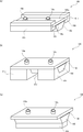
- FIG. 8 is a schematic view showing a modification of the contact temperature control unit. Since the contact-type temperature control unit 60 shown in FIG. 8 has basically the same configuration as the contact-type temperature control unit 60 shown in FIG. Detailed description is omitted.
- the heat transfer member 61b can be configured to cover the upper surface 106a, the side surface 106b, and the lower surface 106c of the flow path forming member 106.
- the heat transfer member 61b may be arranged such that the upper surface 106a, the side surface 106b, and the lower surface 106c of the flow path forming member 106 are sandwiched by a plurality of divided members, or the flow path forming is performed by an integral member. You may arrange
- the heat transfer member 61 b can be configured to cover the dielectric member 102.
- the heat transfer member 61b is provided with a hole 61b ′ in a portion that contacts the incident surface 102a and the emission surface 102c of the dielectric member 102 so as not to disturb the optical path of the excitation light ⁇ .
- the heat transfer member 61b can be configured to contact only the lower surface 102d of the dielectric member 102.
- the temperature control element 61a may be configured to contact the lower surface 102d of the dielectric member 102 without using the heat transfer member 61b.
- FIG. 9 is a schematic diagram showing a modification of the non-contact temperature control unit. Since the non-contact type temperature control unit 70 shown in FIG. 9 has basically the same configuration as the non-contact type temperature control unit 70 shown in FIG. Detailed description thereof will be omitted.
- the non-contact temperature control unit 70 can also be arranged so as to blow heated or cooled air from the horizontal direction with respect to the sensor chip 100. In this way, if it is arranged so as not to interfere with the excitation light irradiation unit 20, the fluorescence detection unit 30, the transport unit 50, etc., air heated or cooled from any direction is blown against the sensor chip 100. It doesn't matter.
- the non-contact temperature control unit 70 blows heated or cooled air to the pipette tip 45, and the sensor chip 100 also receives heated or cooled air. It can also be arranged.
- the non-contact temperature control unit 70 further includes a pipette tip casing 74.
- the pipette tip housing 74 has a pipette tip hole 74a through which the pipette tip 45 passes.
- the pipette tip 45 is inserted into the first through hole 110a of the sensor chip 100 in a state of passing through the pipette tip hole 74a.
- the temperature of the pipette tip 45 and the liquid collected in the pipette tip 45 can be controlled.
- the temperature of the liquid to be introduced into the flow path 112 of the sensor chip 100 can be controlled in advance, or the temperature of the liquid in the pipette tip 45 can be controlled during reciprocating liquid feeding. The accompanying change in the temperature of the reaction field can be suppressed.
- the air blown to the pipette tip 45 blows out from the gap between the pipette tip 45 and the pipette tip hole 74a, and heats or cools the sensor chip 100.
- the temperature of the reaction field is quickly brought close to the reaction field target temperature T, and the reaction field target It becomes easy to maintain the temperature T.
- the non-contact temperature control unit 70 includes a second temperature control means 71 and a second temperature sensor 72 that are infrared heaters that heat the sensor chip 100 by emitting infrared rays. You can also In this case, since the air blowing means 73 is not necessary as the non-contact temperature control unit 70, it is not necessary to consider the influence of wind.
- FIG. 10 is a schematic diagram illustrating a modified example of the sensor chip. Since the sensor chip 100 shown in FIG. 10 has basically the same configuration as the sensor chip 100 shown in FIG. 1, the same components are denoted by the same reference numerals, and detailed description thereof is omitted. .
- the liquid holding member of the sensor chip 100 can be a well member 107.
- the number of wells 107a of the well member 107 may be one as in this embodiment, or a plurality of wells 107a may be arranged in a matrix.
- the non-contact temperature control unit 70 is disposed so that the liquid in the well 107a is not directly exposed to air, or the upper surface opening of the well 107a is protected by a multilayer film or the like, and the pipette tip 45 is It is preferable that the liquid collected while penetrating through the multilayer film is introduced into the well 107a.
- the SPFS apparatus has been described in the above embodiment, but the sample detection system according to the present invention has an SPR. It can be applied to a specimen detection system using a fluorescent immunoassay (FIA) such as an apparatus, a specimen detection system using an enzyme immunoassay (EIA), etc. Can be changed.
- FIA fluorescent immunoassay
- EIA enzyme immunoassay
Landscapes
- Health & Medical Sciences (AREA)
- Chemical & Material Sciences (AREA)
- Immunology (AREA)
- Life Sciences & Earth Sciences (AREA)
- Physics & Mathematics (AREA)
- Analytical Chemistry (AREA)
- General Health & Medical Sciences (AREA)
- Biochemistry (AREA)
- General Physics & Mathematics (AREA)
- Pathology (AREA)
- Engineering & Computer Science (AREA)
- Hematology (AREA)
- Urology & Nephrology (AREA)
- Biomedical Technology (AREA)
- Molecular Biology (AREA)
- Chemical Kinetics & Catalysis (AREA)
- Nuclear Medicine, Radiotherapy & Molecular Imaging (AREA)
- Cell Biology (AREA)
- Microbiology (AREA)
- Biotechnology (AREA)
- Food Science & Technology (AREA)
- Medicinal Chemistry (AREA)
- Clinical Laboratory Science (AREA)
- Optics & Photonics (AREA)
- Dispersion Chemistry (AREA)
- Investigating, Analyzing Materials By Fluorescence Or Luminescence (AREA)
Abstract
Description
このような検体検出方法としては、例えば、試料液に含まれる測定対象物質である抗原と、標識物質で標識された抗体または抗原との抗原抗体反応を利用して、測定対象物質の有無やその量を測定する免疫測定法(イムノアッセイ)が知られている。
例えば、蛍光免疫測定法を利用した検体検出装置としては、ナノメートルレベルなどの微細領域中で電子と光が共鳴することにより、高い光出力を得る現象(表面プラズモン共鳴(SPR:Surface Plasmon Resonance)現象)を応用し、例えば、生体内の極微少なアラナイトの検出を行うようにした表面プラズモン共鳴装置(以下、「SPR装置」とも言う)が挙げられる。
アナライトを捕捉する反応場を内部に有するセンサーチップを用いて、アナライトの検出を行う検体検出システムであって、
前記センサーチップに対して接触して配置される接触式温調ユニットと、
前記センサーチップに対して非接触に配置される非接触式温調ユニットと、を備え、
前記接触式温調ユニットは、第1温調手段と、該第1温調手段と前記センサーチップとの間の温度を測定する第1温度センサーとを備え、前記第1温度センサーの出力値と所定の第1温調手段目標温度とに基づき前記第1温調手段がフィードバック制御され、
前記非接触式温調ユニットは、第2温調手段と、前記第2温調手段と前記センサーチップとの間の温度を測定する第2温度センサーとを備え、前記第2温度センサーの出力値と所定の第2温調手段目標温度とに基づき前記第2温調手段がフィードバック制御される。
図1は、本発明の一実施形態に係る表面プラズモン励起増強蛍光分光測定装置(SPFS装置)の構成を説明するための模式図である。
反応場目標温度Tは、反応場に固定化されたリガンドの種類や、アナライトの種類などによって適宜変更される。反応場目標温度Tは、一般的には、24℃~26℃、もしくは、35℃~37℃に設定することができる。本実施形態において、反応場目標温度Tは36℃である。また、SPFS装置10は室温に設置され、本実施形態において環境温度t3は25℃である。
第1温調手段目標温度T1は、反応場目標温度Tと近い温度に設定することが望ましい。第1温調手段目標温度T1と反応場目標温度Tとの差|T-T1|は、誘電体部材102や伝熱部材61bの材質及び形状などにより、熱伝達の温度勾配を考慮して適宜設定することができる。第1温調手段目標温度T1と反応場目標温度Tとの差|T-T1|を熱伝達の温度勾配程度として、反応場目標温度Tと第1温調手段目標温度T1とを近い温度に設定することで、センサーチップ100が第1温調手段61により過剰に温調されることを防ぎ、反応場を反応場目標温度Tに安定して制御することができる。本実施形態において、第1温調手段目標温度T1は36.5℃であり、第1温調手段目標温度T1と反応場目標温度Tとの差|T-T1|は0.5℃である。


そして制御部80は、送液ユニット40を操作して、流路112内の測定液を排出し、液貯留部材108のウェル108a内の試料液を流路112内に導入する(S180)。流路112内では、抗原抗体反応(1次反応)によって、金属膜104上の反応場にアナライトが捕捉される。
なお、本実施形態では、1次反応(S180)の前に、増強角検出(S150)、光学ブランク値測定(S160)を実施しているが、1次反応(S180)の後に、増強角検出(S150)、光学ブランク値測定(S160)を実施するようにしてもよい。
図4は、本実施形態におけるSPFS装置を用いてセンサーチップの温調を行った際の経過時間と反応場温度との関係を示すグラフである。
この実施例では、下記表1に示す条件でSPFS装置10を動作させ、経過時間と反応場温度を測定した。

実施例1-2及び実施例1-3では、環境温度と反応場目標温度Tとの差が大きいため、検体検出の初期段階である領域1と、2次反応や洗浄など各工程に要する時間が短く、液交換の頻度が高い領域3において、第2温調手段目標温度T2を領域2よりも高く設定している。

領域1では、a=0,b=-0.15,c=41.5
領域3では、a=-0.01,b=0.2,c=40となる条件で第2温調手段目標温度T2を設定し、制御している。
図5は、比較例1として、センサーチップの温調を行った際の経過時間と反応場温度との関係を示すグラフである。
この比較例1で使用したSPFS装置は、上記実施形態におけるSPFS装置10と同一の装置構成であり、下記表2に示すように、各工程における第2温調手段目標温度T2を変更せずに温調を行っている。また、第2温調手段目標温度T2の設定値は、最も厳密な温度制御が必要な領域3において、反応場が反応場目標温度Tとなる値に設定した。

比較例1-2、比較例1-3では、第2温調手段目標温度T2が反応場目標温度Tよりも比較的高い値であるため、反応時間が長い1次反応中(領域2)において、非接触式温調ユニット70による過度な加熱となり、反応場の温度が反応場目標温度Tよりも高くなりすぎてしまった。
図6は、比較例2として、センサーチップの温調を行った際の経過時間と反応場温度との関係を示すグラフである。
この比較例2で使用したSPFS装置は、上記実施形態におけるSPFS装置10と同一の装置構成であり、下記表3に示すように、環境温度によらず、第2温調手段目標温度T2を一定として温調を行っている。

比較例2-2、比較例2-3では、反応場目標温度Tと比較して環境温度が低いため、比較例2-1に比べて各領域での昇温速度が遅く、2次反応中(領域3)の反応場の温度は、反応場目標温度Tに達していない。
図7は、比較例3として、センサーチップの温調を行った際の経過時間と反応場温度との関係を示すグラフである。
この比較例3で使用したSPFS装置は、上記実施形態におけるSPFS装置10と同一の装置構成であり、下記表4に示すように、非接触式温調ユニット70を動作させずに、接触式温調ユニット60のみで温調を行っている。

図8は、接触式温調ユニットの変形例を示す模式図である。図8に示す接触式温調ユニット60は、基本的には、図1に示す接触式温調ユニット60と同様な構成であるため、同一の構成部材には同一の符号を付して、その詳細な説明を省略する。
また、図示しないが、伝熱部材61bを用いず、誘電体部材102の下面102dに温調素子61aを接触するように構成することもできる。
図9は、非接触式温調ユニットの変形例を示す模式図である。図9に示す非接触式温調ユニット70は、基本的には、図1に示す非接触式温調ユニット70と同様な構成であるため、同一の構成部材には同一の符号を付して、その詳細な説明を省略する。
このように、ピペットチップ45、ピペットチップ45内に採取された液体、センサーチップ100を同時に加熱または冷却することにより、反応場の温度を迅速に反応場目標温度Tに近づけ、かつ、反応場目標温度Tに維持することが容易となる。
図10は、センサーチップの変形例を示す模式図である。図10に示すセンサーチップ100は、基本的には、図1に示すセンサーチップ100と同様な構成であるため、同一の構成部材には同一の符号を付して、その詳細な説明を省略する。
12 筐体
13a 吸気口
13b 排気口
14 ファン
15 第3温度センサー
20 励起光照射ユニット
21 光源ユニット
22 角度調整機構
23 光源制御部
30 蛍光検出ユニット
31 受光ユニット
32 レンズ
33 光学フィルター
34 レンズ
35 受光センサー
37 位置切替機構
38 センサー制御部
40 送液ユニット
41 シリンジポンプ
42 シリンジ
43 プランジャー
44 送液ポンプ駆動機構
45 ピペットチップ
46 ピペットノズル
50 搬送ユニット
52 搬送ステージ
54 チップホルダー
60 接触式温調ユニット
61 第1温調手段
61a 温調素子
61b 伝熱部材
61b' 孔部
62 第1温度センサー
70 非接触式温調ユニット
71 第2温調手段
72 第2温度センサー
73 送風手段
74 シリンジ用筐体
74a シリンジ用孔
80 制御部
100 センサーチップ
102 誘電体部材
102a 入射面
102b 成膜面
102c 出射面
102d 下面
104 金属膜
106 流路形成部材
106a 上面
106b 側面
106c 下面
107 ウェル部材
107a ウェル
108 液貯留部材
108a ウェル
110 流路溝
110a 第1貫通孔
110b 第2貫通孔
111 多層フィルム
112 流路
Claims (8)
- アナライトを捕捉する反応場を内部に有するセンサーチップを用いて、アナライトの検出を行う検体検出システムであって、
前記センサーチップに対して接触して配置される接触式温調ユニットと、
前記センサーチップに対して非接触に配置される非接触式温調ユニットと、を備え、
前記接触式温調ユニットは、第1温調手段と、該第1温調手段と前記センサーチップとの間の温度を測定する第1温度センサーとを備え、前記第1温度センサーの出力値と所定の第1温調手段目標温度とに基づき前記第1温調手段がフィードバック制御され、
前記非接触式温調ユニットは、第2温調手段と、該第2温調手段と前記センサーチップとの間の温度を測定する第2温度センサーとを備え、前記第2温度センサーの出力値と所定の第2温調手段目標温度とに基づき前記第2温調手段がフィードバック制御される検体検出システム。 - 前記検体検出システムが設置される環境の温度が測定される第3温度センサーをさらに備え、
前記第3温度センサーの出力値に基づき、前記第2温調手段目標温度が設定される請求項1に記載の検体検出システム。 - 前記第3温度センサーで測定された温度t3と、前記第2温調手段目標温度T2とが、下記式(1)となるように設定される請求項2に記載の検体検出システム。

- 前記反応場の目標温度Tと前記第1温調手段目標温度T1との差|T-T1|と、前記反応場の目標温度Tと前記第2温調手段目標温度T2との差|T-T2|とが、下記式(2)となるように設定される請求項1から3のいずれかに記載の検体検出システム。

- 前記検体検出システムが、複数の工程からなる検体検出手順を実行するように構成され、
前記第2温調手段目標温度T2は、各工程において変更可能である請求項1から4のいずれかに記載の検体検出システム。 - 前記センサーチップに液体を導入する時間が短い工程ほど、前記反応場の目標温度Tと前記第2温調手段目標温度T2との差|T-T2|が大きくなるように、前記第2温調手段目標温度T2が設定される請求項5に記載の検体検出システム。
- 前記センサーチップに液体を導入する送液ユニットをさらに備え、
前記送液ユニットは、前記液体を採取して、前記センサーチップに該液体を供給するノズル及びシリンジポンプを少なくとも含み、
前記非接触式温調ユニットは、内部に液体を吸排する前記ノズルの加熱または冷却を行う請求項1から6のいずれかに記載の検体検出システム。 - 前記センサーチップが、
誘電体部材と、
前記誘電体部材の上面に隣接する金属膜と、
前記金属膜の上面に隣接する反応場と、
前記反応層の上面に配置される液保持部材と、を備えるとともに、
前記検体検出システムが、
前記金属膜に前記誘電体部材を介して励起光を照射する励起光照射ユニットと、
前記金属膜に照射された励起光に基づき、前記反応場に捕捉された蛍光標識された前記アナライトから生じる蛍光を検出する蛍光検出ユニットと、を備える請求項1から7のいずれかに記載の検体検出システム。
Priority Applications (3)
| Application Number | Priority Date | Filing Date | Title |
|---|---|---|---|
| JP2019505788A JP7093766B2 (ja) | 2017-03-17 | 2018-02-15 | 検体検出システム |
| EP18767630.9A EP3598129A4 (en) | 2017-03-17 | 2018-02-15 | SAMPLE DETECTION SYSTEM |
| US16/493,844 US20200124531A1 (en) | 2017-03-17 | 2018-02-15 | Sample detecting system |
Applications Claiming Priority (2)
| Application Number | Priority Date | Filing Date | Title |
|---|---|---|---|
| JP2017-052777 | 2017-03-17 | ||
| JP2017052777 | 2017-03-17 |
Publications (1)
| Publication Number | Publication Date |
|---|---|
| WO2018168308A1 true WO2018168308A1 (ja) | 2018-09-20 |
Family
ID=63523470
Family Applications (1)
| Application Number | Title | Priority Date | Filing Date |
|---|---|---|---|
| PCT/JP2018/005166 Ceased WO2018168308A1 (ja) | 2017-03-17 | 2018-02-15 | 検体検出システム |
Country Status (4)
| Country | Link |
|---|---|
| US (1) | US20200124531A1 (ja) |
| EP (1) | EP3598129A4 (ja) |
| JP (1) | JP7093766B2 (ja) |
| WO (1) | WO2018168308A1 (ja) |
Cited By (3)
| Publication number | Priority date | Publication date | Assignee | Title |
|---|---|---|---|---|
| WO2019230222A1 (ja) * | 2018-06-01 | 2019-12-05 | コニカミノルタ株式会社 | 表面プラズモン励起増強蛍光測定法 |
| US20210106987A1 (en) * | 2018-04-20 | 2021-04-15 | Q-Linea Ab | Analysis instrument and sample preparation cartridge |
| WO2025263386A1 (ja) * | 2024-06-18 | 2025-12-26 | キヤノン株式会社 | 反応測定装置 |
Families Citing this family (3)
| Publication number | Priority date | Publication date | Assignee | Title |
|---|---|---|---|---|
| EP3699601B1 (en) * | 2017-10-16 | 2022-06-08 | Otsuka Pharmaceutical Co., Ltd. | Reaction method |
| JP7249989B2 (ja) * | 2020-12-16 | 2023-03-31 | 日本電子株式会社 | 荷電粒子線装置 |
| CN117074423B (zh) * | 2023-10-16 | 2023-12-12 | 江苏图恩视觉科技有限公司 | 一种薄膜缺陷检测系统及其工作方法 |
Citations (8)
| Publication number | Priority date | Publication date | Assignee | Title |
|---|---|---|---|---|
| WO2003093835A1 (en) * | 2002-04-30 | 2003-11-13 | Arkray, Inc. | Method for adjusting temperature of analyzing tool and analyzing device having function of adjusting temperature |
| JP2006226780A (ja) * | 2005-02-16 | 2006-08-31 | Fuji Photo Film Co Ltd | 全反射減衰を利用した測定装置及びその測定方法 |
| JP2009002801A (ja) * | 2007-06-21 | 2009-01-08 | Olympus Corp | 分注方法及び、それを用いた分注装置 |
| WO2012070557A1 (ja) * | 2010-11-26 | 2012-05-31 | 株式会社日立ハイテクノロジーズ | 自動分析装置 |
| JP2012215465A (ja) | 2011-03-31 | 2012-11-08 | Fujifilm Corp | 分析装置 |
| JP2012215473A (ja) * | 2011-03-31 | 2012-11-08 | Fujifilm Corp | 分析装置および分析チップ、並びに分析装置における温度測定方法 |
| WO2014103744A1 (ja) * | 2012-12-26 | 2014-07-03 | 株式会社 日立ハイテクノロジーズ | 自動分析装置 |
| WO2015064757A1 (ja) * | 2013-10-31 | 2015-05-07 | コニカミノルタ株式会社 | 検出装置、当該検出装置を用いた検出方法および当該検出装置に用いられる検出チップ |
Family Cites Families (2)
| Publication number | Priority date | Publication date | Assignee | Title |
|---|---|---|---|---|
| US8120777B2 (en) * | 2007-12-10 | 2012-02-21 | Molecular Sensing, Inc. | Temperature-stable interferometer |
| US11079331B2 (en) * | 2015-11-13 | 2021-08-03 | Konica Minolta, Inc. | Inspection system |
-
2018
- 2018-02-15 US US16/493,844 patent/US20200124531A1/en not_active Abandoned
- 2018-02-15 EP EP18767630.9A patent/EP3598129A4/en not_active Withdrawn
- 2018-02-15 JP JP2019505788A patent/JP7093766B2/ja active Active
- 2018-02-15 WO PCT/JP2018/005166 patent/WO2018168308A1/ja not_active Ceased
Patent Citations (8)
| Publication number | Priority date | Publication date | Assignee | Title |
|---|---|---|---|---|
| WO2003093835A1 (en) * | 2002-04-30 | 2003-11-13 | Arkray, Inc. | Method for adjusting temperature of analyzing tool and analyzing device having function of adjusting temperature |
| JP2006226780A (ja) * | 2005-02-16 | 2006-08-31 | Fuji Photo Film Co Ltd | 全反射減衰を利用した測定装置及びその測定方法 |
| JP2009002801A (ja) * | 2007-06-21 | 2009-01-08 | Olympus Corp | 分注方法及び、それを用いた分注装置 |
| WO2012070557A1 (ja) * | 2010-11-26 | 2012-05-31 | 株式会社日立ハイテクノロジーズ | 自動分析装置 |
| JP2012215465A (ja) | 2011-03-31 | 2012-11-08 | Fujifilm Corp | 分析装置 |
| JP2012215473A (ja) * | 2011-03-31 | 2012-11-08 | Fujifilm Corp | 分析装置および分析チップ、並びに分析装置における温度測定方法 |
| WO2014103744A1 (ja) * | 2012-12-26 | 2014-07-03 | 株式会社 日立ハイテクノロジーズ | 自動分析装置 |
| WO2015064757A1 (ja) * | 2013-10-31 | 2015-05-07 | コニカミノルタ株式会社 | 検出装置、当該検出装置を用いた検出方法および当該検出装置に用いられる検出チップ |
Non-Patent Citations (1)
| Title |
|---|
| See also references of EP3598129A4 |
Cited By (4)
| Publication number | Priority date | Publication date | Assignee | Title |
|---|---|---|---|---|
| US20210106987A1 (en) * | 2018-04-20 | 2021-04-15 | Q-Linea Ab | Analysis instrument and sample preparation cartridge |
| US12318772B2 (en) * | 2018-04-20 | 2025-06-03 | Q-Linea Ab | Analysis instrument and sample preparation cartridge |
| WO2019230222A1 (ja) * | 2018-06-01 | 2019-12-05 | コニカミノルタ株式会社 | 表面プラズモン励起増強蛍光測定法 |
| WO2025263386A1 (ja) * | 2024-06-18 | 2025-12-26 | キヤノン株式会社 | 反応測定装置 |
Also Published As
| Publication number | Publication date |
|---|---|
| US20200124531A1 (en) | 2020-04-23 |
| JP7093766B2 (ja) | 2022-06-30 |
| EP3598129A1 (en) | 2020-01-22 |
| JPWO2018168308A1 (ja) | 2020-01-16 |
| EP3598129A4 (en) | 2020-03-11 |
Similar Documents
| Publication | Publication Date | Title |
|---|---|---|
| JP7093766B2 (ja) | 検体検出システム | |
| JP6337905B2 (ja) | 表面プラズモン共鳴蛍光分析方法および表面プラズモン共鳴蛍光分析装置 | |
| EP3674694B1 (en) | Analysis method and analysis device | |
| JP6399089B2 (ja) | 表面プラズモン共鳴蛍光分析方法、表面プラズモン共鳴蛍光分析装置および位置合わせ方法 | |
| JP6424890B2 (ja) | 表面プラズモン増強蛍光測定方法、表面プラズモン増強蛍光測定装置および分析チップ | |
| JP6648764B2 (ja) | 反応方法 | |
| JP7121742B2 (ja) | 回折光除去スリットを用いた光学式検体検出システム | |
| JP6848878B2 (ja) | 検出装置、検出方法および検出システム | |
| JPWO2019221040A1 (ja) | 検体検出チップ及びこれを用いた検体検出装置 | |
| JP7050776B2 (ja) | 検体検出装置及び検体検出方法 | |
| JP7093727B2 (ja) | 光学式検体検出システムにおけるセンサーチップの位置検出方法及び位置検出装置 | |
| JP6885458B2 (ja) | 検体検出システム用センサーチップ | |
| JP6658752B2 (ja) | 検出チップ、検出方法、検出装置および検出システム |
Legal Events
| Date | Code | Title | Description |
|---|---|---|---|
| 121 | Ep: the epo has been informed by wipo that ep was designated in this application |
Ref document number: 18767630 Country of ref document: EP Kind code of ref document: A1 |
|
| ENP | Entry into the national phase |
Ref document number: 2019505788 Country of ref document: JP Kind code of ref document: A |
|
| NENP | Non-entry into the national phase |
Ref country code: DE |
|
| WWE | Wipo information: entry into national phase |
Ref document number: 2018767630 Country of ref document: EP |
|
| ENP | Entry into the national phase |
Ref document number: 2018767630 Country of ref document: EP Effective date: 20191017 |