WO2018174139A1 - ダイヤモンド被覆超硬合金切削工具 - Google Patents
ダイヤモンド被覆超硬合金切削工具 Download PDFInfo
- Publication number
- WO2018174139A1 WO2018174139A1 PCT/JP2018/011328 JP2018011328W WO2018174139A1 WO 2018174139 A1 WO2018174139 A1 WO 2018174139A1 JP 2018011328 W JP2018011328 W JP 2018011328W WO 2018174139 A1 WO2018174139 A1 WO 2018174139A1
- Authority
- WO
- WIPO (PCT)
- Prior art keywords
- diamond
- substrate
- diamond film
- film
- cemented carbide
- Prior art date
- Legal status (The legal status is an assumption and is not a legal conclusion. Google has not performed a legal analysis and makes no representation as to the accuracy of the status listed.)
- Ceased
Links
Images


Classifications
-
- C—CHEMISTRY; METALLURGY
- C23—COATING METALLIC MATERIAL; COATING MATERIAL WITH METALLIC MATERIAL; CHEMICAL SURFACE TREATMENT; DIFFUSION TREATMENT OF METALLIC MATERIAL; COATING BY VACUUM EVAPORATION, BY SPUTTERING, BY ION IMPLANTATION OR BY CHEMICAL VAPOUR DEPOSITION, IN GENERAL; INHIBITING CORROSION OF METALLIC MATERIAL OR INCRUSTATION IN GENERAL
- C23C—COATING METALLIC MATERIAL; COATING MATERIAL WITH METALLIC MATERIAL; SURFACE TREATMENT OF METALLIC MATERIAL BY DIFFUSION INTO THE SURFACE, BY CHEMICAL CONVERSION OR SUBSTITUTION; COATING BY VACUUM EVAPORATION, BY SPUTTERING, BY ION IMPLANTATION OR BY CHEMICAL VAPOUR DEPOSITION, IN GENERAL
- C23C30/00—Coating with metallic material characterised only by the composition of the metallic material, i.e. not characterised by the coating process
- C23C30/005—Coating with metallic material characterised only by the composition of the metallic material, i.e. not characterised by the coating process on hard metal substrates
-
- C—CHEMISTRY; METALLURGY
- C23—COATING METALLIC MATERIAL; COATING MATERIAL WITH METALLIC MATERIAL; CHEMICAL SURFACE TREATMENT; DIFFUSION TREATMENT OF METALLIC MATERIAL; COATING BY VACUUM EVAPORATION, BY SPUTTERING, BY ION IMPLANTATION OR BY CHEMICAL VAPOUR DEPOSITION, IN GENERAL; INHIBITING CORROSION OF METALLIC MATERIAL OR INCRUSTATION IN GENERAL
- C23C—COATING METALLIC MATERIAL; COATING MATERIAL WITH METALLIC MATERIAL; SURFACE TREATMENT OF METALLIC MATERIAL BY DIFFUSION INTO THE SURFACE, BY CHEMICAL CONVERSION OR SUBSTITUTION; COATING BY VACUUM EVAPORATION, BY SPUTTERING, BY ION IMPLANTATION OR BY CHEMICAL VAPOUR DEPOSITION, IN GENERAL
- C23C16/00—Chemical coating by decomposition of gaseous compounds, without leaving reaction products of surface material in the coating, i.e. chemical vapour deposition [CVD] processes
- C23C16/22—Chemical coating by decomposition of gaseous compounds, without leaving reaction products of surface material in the coating, i.e. chemical vapour deposition [CVD] processes characterised by the deposition of inorganic material, other than metallic material
- C23C16/26—Deposition of carbon only
- C23C16/27—Diamond only
-
- B—PERFORMING OPERATIONS; TRANSPORTING
- B23—MACHINE TOOLS; METAL-WORKING NOT OTHERWISE PROVIDED FOR
- B23B—TURNING; BORING
- B23B27/00—Tools for turning or boring machines; Tools of a similar kind in general; Accessories therefor
- B23B27/14—Cutting tools of which the bits or tips or cutting inserts are of special material
-
- B—PERFORMING OPERATIONS; TRANSPORTING
- B23—MACHINE TOOLS; METAL-WORKING NOT OTHERWISE PROVIDED FOR
- B23B—TURNING; BORING
- B23B27/00—Tools for turning or boring machines; Tools of a similar kind in general; Accessories therefor
- B23B27/14—Cutting tools of which the bits or tips or cutting inserts are of special material
- B23B27/148—Composition of the cutting inserts
-
- B—PERFORMING OPERATIONS; TRANSPORTING
- B23—MACHINE TOOLS; METAL-WORKING NOT OTHERWISE PROVIDED FOR
- B23B—TURNING; BORING
- B23B27/00—Tools for turning or boring machines; Tools of a similar kind in general; Accessories therefor
- B23B27/14—Cutting tools of which the bits or tips or cutting inserts are of special material
- B23B27/18—Cutting tools of which the bits or tips or cutting inserts are of special material with cutting bits or tips or cutting inserts rigidly mounted, e.g. by brazing
- B23B27/20—Cutting tools of which the bits or tips or cutting inserts are of special material with cutting bits or tips or cutting inserts rigidly mounted, e.g. by brazing with diamond bits or cutting inserts
-
- B—PERFORMING OPERATIONS; TRANSPORTING
- B23—MACHINE TOOLS; METAL-WORKING NOT OTHERWISE PROVIDED FOR
- B23B—TURNING; BORING
- B23B51/00—Tools for drilling machines
-
- B—PERFORMING OPERATIONS; TRANSPORTING
- B23—MACHINE TOOLS; METAL-WORKING NOT OTHERWISE PROVIDED FOR
- B23C—MILLING
- B23C5/00—Milling-cutters
- B23C5/16—Milling-cutters characterised by physical features other than shape
-
- C—CHEMISTRY; METALLURGY
- C01—INORGANIC CHEMISTRY
- C01B—NON-METALLIC ELEMENTS; COMPOUNDS THEREOF; METALLOIDS OR COMPOUNDS THEREOF NOT COVERED BY SUBCLASS C01C
- C01B32/00—Carbon; Compounds thereof
- C01B32/25—Diamond
- C01B32/26—Preparation
-
- C—CHEMISTRY; METALLURGY
- C23—COATING METALLIC MATERIAL; COATING MATERIAL WITH METALLIC MATERIAL; CHEMICAL SURFACE TREATMENT; DIFFUSION TREATMENT OF METALLIC MATERIAL; COATING BY VACUUM EVAPORATION, BY SPUTTERING, BY ION IMPLANTATION OR BY CHEMICAL VAPOUR DEPOSITION, IN GENERAL; INHIBITING CORROSION OF METALLIC MATERIAL OR INCRUSTATION IN GENERAL
- C23C—COATING METALLIC MATERIAL; COATING MATERIAL WITH METALLIC MATERIAL; SURFACE TREATMENT OF METALLIC MATERIAL BY DIFFUSION INTO THE SURFACE, BY CHEMICAL CONVERSION OR SUBSTITUTION; COATING BY VACUUM EVAPORATION, BY SPUTTERING, BY ION IMPLANTATION OR BY CHEMICAL VAPOUR DEPOSITION, IN GENERAL
- C23C16/00—Chemical coating by decomposition of gaseous compounds, without leaving reaction products of surface material in the coating, i.e. chemical vapour deposition [CVD] processes
- C23C16/02—Pretreatment of the material to be coated
- C23C16/0227—Pretreatment of the material to be coated by cleaning or etching
-
- C—CHEMISTRY; METALLURGY
- C23—COATING METALLIC MATERIAL; COATING MATERIAL WITH METALLIC MATERIAL; CHEMICAL SURFACE TREATMENT; DIFFUSION TREATMENT OF METALLIC MATERIAL; COATING BY VACUUM EVAPORATION, BY SPUTTERING, BY ION IMPLANTATION OR BY CHEMICAL VAPOUR DEPOSITION, IN GENERAL; INHIBITING CORROSION OF METALLIC MATERIAL OR INCRUSTATION IN GENERAL
- C23C—COATING METALLIC MATERIAL; COATING MATERIAL WITH METALLIC MATERIAL; SURFACE TREATMENT OF METALLIC MATERIAL BY DIFFUSION INTO THE SURFACE, BY CHEMICAL CONVERSION OR SUBSTITUTION; COATING BY VACUUM EVAPORATION, BY SPUTTERING, BY ION IMPLANTATION OR BY CHEMICAL VAPOUR DEPOSITION, IN GENERAL
- C23C16/00—Chemical coating by decomposition of gaseous compounds, without leaving reaction products of surface material in the coating, i.e. chemical vapour deposition [CVD] processes
- C23C16/22—Chemical coating by decomposition of gaseous compounds, without leaving reaction products of surface material in the coating, i.e. chemical vapour deposition [CVD] processes characterised by the deposition of inorganic material, other than metallic material
- C23C16/26—Deposition of carbon only
- C23C16/27—Diamond only
- C23C16/271—Diamond only using hot filaments
-
- C—CHEMISTRY; METALLURGY
- C01—INORGANIC CHEMISTRY
- C01B—NON-METALLIC ELEMENTS; COMPOUNDS THEREOF; METALLOIDS OR COMPOUNDS THEREOF NOT COVERED BY SUBCLASS C01C
- C01B32/00—Carbon; Compounds thereof
- C01B32/90—Carbides
- C01B32/914—Carbides of single elements
- C01B32/949—Tungsten or molybdenum carbides
Definitions
- the present invention exhibits excellent chipping resistance and peel resistance by providing excellent impact resistance and adhesion in high-speed cutting of difficult-to-cut materials such as CFRP (carbon fiber reinforced plastic), and tool life.
- the present invention relates to a cutting tool made of diamond-coated tungsten carbide (WC) -based cemented carbide with improved resistance.
- diamond-coated tool in which a tool base made of a WC-based cemented carbide (hereinafter referred to as “superhard alloy”) is coated with a diamond film
- superhard alloy a tool base made of a WC-based cemented carbide
- various proposals have been made such as forming a diamond film on the tool base.
- Patent Document 1 discloses a cutting tool obtained by coating a surface of a cemented carbide substrate having irregularities with a diamond film through an intermediate layer that prevents diffusion of components of the cemented carbide substrate. ing.
- Patent Document 2 discloses that a diamond film is laminated so that the crystal grain size of the surface is 2 ⁇ m or less in order to perform processing with high surface processing accuracy.
- Patent Document 2 describes the roughness of the machined surface of a nonferrous metal such as an aluminum alloy, but does not describe application to difficult-to-cut materials such as CFRP. If the ratio of the fine crystal grains of the tool surface diamond is increased, the wear resistance may be lowered, and cannot be immediately applied to difficult-to-cut materials such as CFRP.
- the technical problem to be solved by the present invention is to improve the adhesion between the diamond coating and the tool base in the diamond-coated tool and improve the edge strength (impact resistance) of the diamond-coated tool.
- An object of the present invention is to provide a diamond-coated tool having a long cutting life and improved chipping resistance and peeling resistance in high-speed cutting of difficult-to-cut materials such as CFRP.
- the roughness of the interface of the cemented carbide substrate is predetermined, and the crystal grain size in the initial stage of the growth of the diamond film is in a predetermined range.
- the present invention “(1) A diamond-coated cemented carbide cutting tool in which a diamond film is formed on a WC-based cemented carbide substrate containing 3 to 15 mass% of Co, In the cut surface in the diamond film thickness direction of the diamond coated cemented carbide cutting tool, (A) The WC particles constituting the substrate have an average particle size of 0.5 to 0.9 ⁇ m, (B) The maximum height difference (R z ) of the irregularities at the interface of the substrate in contact with the diamond film is 0.5 to 1.0 ⁇ m, and the maximum value of the distance between the irregularities of the adjacent substrates at the interface ( ⁇ ) Is 0.5 to 1.5 ⁇ m, and the length (Y e ) in the thickness direction of the diamond film in the region where the binder phase of the substrate is removed is 0.5 to 2.0 ⁇ m, (C) When the sum of the areas occupied by the individual WC particles in contact with the diamond film at the interface is 100% by area, the maximum value (L 1 ) of the distance between the vertices
- the present invention can improve the adhesion of the diamond coating to the tool substrate, reduce the distortion contained in the diamond coating, and achieve high smoothness of the outer surface, so that the chipping of the diamond-coated cutting tool can be achieved. Can be suppressed, and the remarkable effect of extending the life of the cutting tool can be achieved.
- FIG. 1 It is a schematic diagram of a cross section in the thickness direction (longitudinal section) of a diamond film showing that the unevenness of the substrate of the cemented carbide has an influence on the unevenness of the diamond film.
- FIG. 1 It is the schematic diagram which expanded the longitudinal cross-section of the diamond-coated tool which concerns on one Embodiment of this invention (Because it is a schematic diagram, the scale is not accurate, and in order to emphasize the presence of a binder phase, the area is displayed larger than actual. ) It is a figure explaining the distance between the unevenness
- FIG. 3 is a schematic diagram of the shape of the WC particle in the region from which the binder phase is removed in FIG. 2, and is the maximum value (L 1 ) of the distance between the vertices of the WC particle diameter and the diameter of the inscribed circle inscribed in the WC particle or is a diagram illustrating the minimum distance (L 2) between tangents.
- the present invention suppresses chipping of the diamond coating tool by improving the adhesion of the diamond coating to the tool base, reducing the included strain, and high smoothness of the outer surface. This is based on the new knowledge of improving the peeling resistance of the diamond film and extending the tool life.
- the adhesiveness of the diamond film is determined by (1) Co content, (2) Average particle diameter of WC particles, (3) Maximum height difference of irregularities at the substrate interface in the WC-based cemented carbide substrate as a substrate ( R z ), (4) the distance ( ⁇ ) between the maximum irregularities of adjacent substrates at the interface, (5) the length (Y e ) in the thickness direction of the diamond film in the region where the binder phase of the substrate has been removed, (6) The maximum value (L 1 ) of the distance between the vertices of the WC particles in contact with the diamond film at the interface, the diameter of the inscribed circle inscribed in the WC particles, or the minimum distance (L 2 ) between the tangents of the opposing surface, (7 This is achieved by setting each factor of (L 1 ) / (L 2 ) and (8) the area ratio of WC particles corresponding to (6) and (7) above to a predetermined value.
- the smoothness of the surface of the diamond film is such that, in addition to setting the factor affecting the adhesion to a predetermined value, (9) diamond in the region of 0.5 to 1.5 ⁇ m from the substrate interface toward the diamond film.
- the average grain size of the crystal is 0.1 to 0.3 ⁇ m, (10) in contact with the diamond crystal (in contact with the diamond crystal described in (9) above), and the growth direction is the thickness of the diamond film.
- 90% or more, or ⁇ 110> orientation ratio is 30% or more (the ratio of columnar crystals whose angle between the growth direction and the thickness direction of the diamond film is within 10 degrees) with respect to the vertical direction. This is achieved by having columnar crystals constituting a diamond film that is at least one of ⁇ 70%.
- the diamond film controls factors affecting the adhesion force in order to obtain a predetermined adhesion force, while taking into consideration the influence of the factors affecting the adhesion force on the smoothness.
- factors affecting the adhesion force in order to improve adhesion, reduce the included strain, and improve smoothness, find the optimal range of each of the above factors, suppress chipping and improve peeling resistance, and have a long tool life Obtaining a coated cemented carbide cutting tool has the characteristics of the invention.
- the WC-based cemented carbide substrate 1 of the present embodiment contains WC and Co, and the Co content is 3 to 15% by mass.
- the reason for determining the numerical range of the Co content is as follows.
- the content of Co in the cemented carbide constituting the substrate 1 is less than 3% by mass, the toughness of the tool substrate 1 is lowered and defects are likely to occur during cutting, which is not preferable.
- the volume ratio occupied by the voids in the area where Co is removed after etching is increased, and the area where Co is removed becomes brittle, so the adhesion between the diamond film and the tool surface decreases. It is not preferable.
- the Co content in the cemented carbide is determined to be 3 to 15% by mass.
- the Co content is preferably 5 to 7% by mass.
- the WC average particle diameter of the WC-based cemented carbide substrate 1 of the present embodiment is 0.5 to 0.9 ⁇ m.
- the reason why the average particle diameter is in this range is that if it is less than 0.5 ⁇ m, the toughness of the substrate 1 is lowered, whereas if it exceeds 0.9 ⁇ m, the unevenness of the substrate after etching in the pretreatment process becomes large and the diamond film 2 is smooth. This is because it adversely affects sex and tends to cause chipping.
- the average particle diameter of WC is preferably 0.6 to 0.8 ⁇ m.
- the particle size of WC is the same at an arbitrary portion of the substrate 1 that has not been subjected to the etching treatment, and is determined as follows.
- the cross-section (the direction of the thickness of the diamond coating 2 (the direction perpendicular to the surface of the diamond coating 2)) of a 50 ⁇ m square region on the substrate side that is 10 ⁇ m away from the surface of the substrate 1 (interface 3 with the diamond coating 2).
- the crystal orientation of each WC particle 1a that has not been subjected to the etching treatment is measured on the condition of a step size of 0.1 ⁇ m using an electron back scatter diffraction pattern (EBSD). Then, a portion where the crystal orientations of adjacent measurement points are shifted by 5 degrees is regarded as a grain boundary, and a region surrounded by the grain boundary is defined as one particle.
- EBSD electron back scatter diffraction pattern
- the number of WC particles 1a included in the 10 ⁇ m line segment (overlapping the 10 ⁇ m line segment) is counted, and 10 ⁇ m is divided by the number of WC particles 1a obtained.
- the average value of the obtained three numerical values is taken as the average particle diameter of WC.
- Rz is in this range. if it is less than 0.5 ⁇ m, the anchor effect of the substrate interface with respect to the diamond coating 2 is not sufficient, and sufficient adhesion of the diamond coating 2 to the substrate 1 may not be obtained. On the other hand, if the thickness exceeds 1.0 ⁇ m, the smoothness of the diamond coating is adversely affected, and chipping is likely to occur.
- the maximum height difference (R z ) is preferably 0.6 to 0.8 ⁇ m.
- ⁇ is preferably 0.7 to 1.2 ⁇ m.
- ⁇ is defined as the distance between the projections and depressions where the height difference satisfies the range of 0.5 to 1.5 ⁇ m. See FIG. 3 for the distance between the irregularities.
- Ye is less than 0.5 ⁇ m
- the Co layer is not sufficiently removed from the surface of the cemented carbide substrate, so that Co diffuses to the interface 3 between the cemented carbide substrate 1 and the coating 2 during diamond film formation, The adhesion of the diamond film 2 is reduced.
- the value of Y e is preferably 0.7 ⁇ 1.5 [mu] m.
- the maximum value (L 1 ) of the distance between the vertices of the WC particles on the substrate interface and the minimum value (L 2 ) of the diameter of the inscribed circle inscribed in the WC particles of the particles or the tangent line of the opposite surface L 1 represents the value of the maximum distance (maximum length) connecting the vertices of the WC particles 1a, and is 0.4 to 0.8 ⁇ m.
- the maximum length (L 1 ) of the WC particle 1a depends on the particle size of the WC particle 1a, and the WC is eroded by etching. Therefore, the range is defined as not exceeding the particle size of the WC. Good adhesion of the diamond film 2 cannot be obtained.
- L 1 is preferably 0.5 to 0.7 ⁇ m.
- L 2 is the minimum value of the distance between the tangent line of the WC of the inscribed circle inscribing the particle 1a diameter or opposing surfaces.
- L 2 is the maximum value of the diameter of the inscribed circle inscribed in the WC particle when there are three vertices constituting the cross-sectional shape of the WC particle 1a of the particle, and the cross-sectional shape of the WC particle 1a of the particle Is the minimum value of the distance between the tangents of the opposing surfaces (sides facing each other in the cross section).
- Range of L 2 is 0.2 ⁇ 0.4 .mu.m.
- L 2 is less than 0.2 ⁇ m, the substrate strength in the region where the binder phase 1b of the substrate 1 is removed cannot be obtained, and cracks are likely to occur in the region of the substrate 1 where the binder phase 1b is removed.
- L 2 exceeds 0.4 ⁇ m, the anchor effect of the substrate interface with respect to the diamond film 2 cannot be sufficiently obtained, and there is a possibility that sufficient adhesion to the substrate 1 cannot be obtained.
- L 2 is preferably 0.25 to 0.35 ⁇ m. Refer to FIG.
- (L 1 ) / (L 2 ) is preferably 1.7 to 2.2. Note that the maximum value (L 1 ) of the distance between the vertices of the WC particles 1a at the substrate interface and the minimum value (L 2 ) of the diameter of the inscribed circle inscribed in the WC particles 1a of the particles or the tangents of the opposing surfaces.
- the crystal orientation is measured under the condition of 0.1 ⁇ m in size, the portion where the crystal orientation of adjacent measurement points is shifted by 5 degrees is regarded as a grain boundary, and the region surrounded by the grain boundary is regarded as one grain of the WC particle 1a.
- (L 1 ) and (L 2 ) of the particles in the same longitudinal section were determined.
- Area ratio of WC particles satisfying the above (6) and (7) includes the interface 3 between the diamond film 2 and the substrate 1.
- the sum of the areas occupied by the individual WC particles 1a in contact with the diamond film 2 at the interface 3 in the longitudinal cross-section (cut surface along the thickness direction of the diamond film) obtained by observing three 50 ⁇ m square regions. If the area occupied by the WC particles 1a satisfying the above (6) and (7) among these WC particles 1a is not more than 70% by area, the definition of the above (6) and (7) However, the adhesion and smoothness of the diamond film 2 cannot be obtained.
- the area ratio is preferably 85 area% or more, more preferably 90 to 100 area%.
- the average film thickness of the diamond film 2 is an average value of five points of the film thickness measured in a region of 50 ⁇ m in the horizontal direction (direction parallel to the substrate surface) with the substrate surface.
- the value is desirably 3 to 30 ⁇ m. By setting it within this range, sufficient wear resistance and peel resistance can be exhibited over a long period of use, the blade is more reliably prevented from being rounded, and a predetermined processing accuracy can be obtained.
- the average film thickness of the diamond film 2 is more preferably 8 to 18 ⁇ m.
- the average grain diameter of the diamond crystal is included in a 3 ⁇ m line segment at each of three arbitrary points in the initial growth region observed by angle selective backscattered electron (hereinafter referred to as ASB).
- ASB angle selective backscattered electron
- the reason for this numerical range is that if it is less than 0.1 ⁇ m, satisfactory adhesion cannot be obtained, and if it exceeds 0.3 ⁇ m, the diamond particles on the outer surface side of the grains are columnar, that is, the diamond film 2 This is because it does not grow in the thickness direction.
- the average grain size of diamond crystals in the initial growth region of the diamond coating 2 is preferably 0.15 to 0.25 ⁇ m.
- the tissue can be confirmed by tissue observation by ASB.
- the diamond film 2 grows in a columnar shape in the late stage 2a of the diamond film growth, and the crystal grain size has a growth ratio (hereinafter referred to as an aspect ratio) in the film thickness direction with respect to the lateral direction exceeding 3, and the aspect ratio increases with the film thickness.
- the deviation in the growth direction of the crystal grains of the film 2 and the ⁇ 110> orientation ratio are measured as follows.
- the growth direction of the diamond coating 2 is that the cutting edge of the diamond coating tool is cut, the cross section of the cutting edge (cut surface along the thickness direction of the diamond coating) is polished with CP, and the area of the coating cross section of 30 ⁇ m square by ASB.
- the area occupied by the crystal whose deviation in the growth direction of the film 2 (long axis direction of the columnar crystal) is within 10 degrees with respect to the film thickness direction is measured region
- the value divided by the total area of the inner coating 2 is defined as the rate of angle deviation within 10 degrees.
- an electron beam is irradiated on each of the crystal grains existing within the measurement range of the polished surface of the film cross section perpendicular to the three film surfaces by means of EBSD.
- the inclination angle between the normal of the plane and the film thickness direction is measured, and the sum of the frequencies where the inclination angle is in the range of 0 to 20 ° is defined as the ⁇ 110> orientation rate.
- the proportion of diamond crystals whose growth direction measured by the above method is within 10 degrees with respect to the normal direction of the substrate 1 (the thickness direction of the diamond film) is 90 °. % Or more, or at least one of ⁇ 110> orientation ratio of 30 to 70%.
- the reason for this numerical range is that if the proportion of the columnar crystals whose growth direction is in the thickness direction of the diamond film 2 is less than 90%, the diamond crystals are shattered at the time of cutting because of the distortion included in the diamond film 2. This is because chipping becomes prominent and chipping is likely to occur. Further, if the ⁇ 110> orientation ratio is less than 30%, the wear resistance of the diamond film 2 is insufficient, and if it exceeds 70%, the diamond crystal grains become coarse and impact resistance is lowered, and chipping is likely to occur. Because.
- the area occupied by the crystals whose deviation in the growth direction of the film 2 is within 10 degrees exceeds 90%.
- a predetermined cutting performance can be obtained.
- the predetermined cutting performance is obtained. can get. Therefore, what is necessary is just to satisfy at least one of both.
- the ratio of columnar crystals with a deviation in angle of the growth direction with respect to the thickness direction of the diamond coating 2 within 10 degrees is preferably 93% or more, and more preferably 95% or more and 100% or less.
- the ⁇ 110> orientation ratio is preferably 40% or more and 60% or less.
- a diamond-coated end mill will be described as a specific example of the diamond-coated tool according to the present invention, but the present invention is not limited to this, and can be applied to various diamond-coated tools such as diamond-coated alloy inserts and diamond-coated drills. Needless to say.
- Substrate manufacturing process WC powder, Co powder, TaC powder, NbC powder or Cr 3 C 2 powder having a predetermined average particle size in the range of 0.5 to 0.9 ⁇ m is used as a raw material powder.
- paraffin as a binder and toluene, xylene, mesitylene, tetralin, or decalin as a binder were added, followed by ball mill mixing in acetone for 24 hours, followed by drying under reduced pressure. Thereafter, both of them were extrusion press-molded to form round bar green compacts having a diameter of 10 mm and a length of 150 mm. These round bar green compacts were placed in a 1 Pa vacuum atmosphere at a temperature of 1380 to 1500 ° C.
- end mill substrate a WC cemented carbide end mill substrate
- (B) Etching treatment step Next, on the surface of the end mill base, the numerical values of R z , ⁇ , L 1 , L 2 , (L 1 ) / (L 2 ), and area% are satisfied. Etching was performed to form fine irregularities.
- the etching process has two stages, an alkali etching process and an acid etching process.
- the alkali etching process is performed by electrolytic etching
- the acid etching process is performed by immersing the substrate in dilute nitric acid. Specifically, it is as follows.
- (C) Pretreatment step for forming a diamond film As a pretreatment for forming a diamond film, an end mill substrate subjected to the above etching treatment is made to have a particle diameter of 1 ⁇ m in order to promote diamond nucleation at the initial stage of diamond film formation. Sonication was performed for 10 minutes in an ethyl alcohol solution containing diamond powder.
- (D) Film-forming process The pre-processed end mill substrate was charged into a hot filament CVD apparatus. Then, the flow rate ratio of hydrogen gas to methane gas is adjusted under a filament temperature of 2050 to 2100 ° C. and a gas pressure of 1 to 3 Torr (133.3 to 399.9 Pa), and the substrate temperature is set to a predetermined value of 750 to 800 ° C.
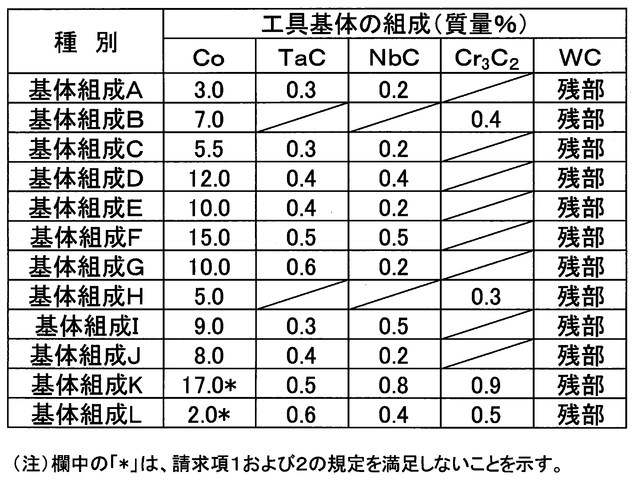
- a raw material powder containing WC powder having a predetermined average particle diameter in the range of 0.4 to 1.2 ⁇ m is blended in the ratio shown in Table 1, and in the step described in (a) above, A drill base was produced. Thereafter, processes corresponding to the above (b) to (d) (details are described in Table 2) were performed, and a comparative diamond film end mill (hereinafter referred to as “comparative end mill”) was prepared.
- the “preceding pretreatment step” in Table 2 is to remove a part of the binder phase near the substrate surface at room temperature (23 ° C.) for 8 to 15 seconds in 1 L of dilute nitric acid (0.5% by volume) solution. Yes, it precedes the aforementioned first pretreatment step.
- Table 2 The diagonal lines in Table 2 indicate that the corresponding process was not performed.
- the comparative end mill 15 and the comparative end mill 18 did not obtain a diamond film.
- Table 3 shows the WC grain size, R z , ⁇ , Y e , L 1 , L 2 , (L 1 ) / (L 2 ) of the substrate in the present invention and the comparative end mill obtained according to Table 2, and , The area percentage of WC particles, the average film thickness of the diamond film, the particle diameter in the region of 0.5 to 1.5 ⁇ m, the ratio of columnar crystals within 10 degrees, and the ⁇ 110> orientation rate.
- the hatched lines indicate that the corresponding item could not be measured.
- the normal cutting speed described in the following conditions is a cutting speed at which the efficiency (generally, the number of parts that can be processed before the tool life) is optimized when a conventional coated tool is used.
- Cutting speed 300 m / min
- Cutting condition Air blow protrusion length: 25mm Feed per tooth: 0.03mm / tooth
- the test was interrupted and the presence / absence of peeling / deficiency was confirmed.
- the processing length up to that time is defined as the processing life. Also, it does not break up to 25m length, the wear form on the flank in the center of the cutting edge is normal (no chipping or chipping), and the burr length or delamination width around the hole exceeds 1mm.
- the absence condition was regarded as a pass condition for the end mill of the present invention. Table 4 shows the evaluation results.
- the Co content constituting the substrate and the average particle diameter of the WC particles are both in a predetermined range, and the maximum height difference of the unevenness at the substrate interface in contact with the diamond film
- the maximum distance between the irregularities, the length in the thickness direction of the diamond film in the region where the binder phase of the substrate has been removed are each in a predetermined range, and further, WC particles of 70 area% or more of the interface are The maximum value of the distance between vertices within a predetermined range, the diameter of the inscribed inscribed circle or the minimum value of the distance between the tangents of the opposing surface, (the maximum value of the distance between the vertices of the WC particles on the substrate interface) / (inside the WC particles)
- the diameter of the inscribed circle in contact or the minimum value of the distance between the tangents of the opposing surface) and the average film thickness of the diamond film and the maximum height difference of the irregularities, 0.5 to 1.5 ⁇ m from
- the diamond-coated cemented carbide cutting tool of the present invention has improved tool life compared to difficult-to-cut materials such as CFRP because it shows excellent chipping resistance and wear resistance. Has been.
- the comparison end mill lacking one or more matters to be satisfied by the diamond-coated cemented carbide cutting tool of the present invention cannot ensure the adhesion and smoothness of the diamond film, so the cutting length is short, It can be seen that chipping occurs and the tool life is short.
- the diamond-coated cemented carbide cutting tool of the present invention is applicable not only to diamond-coated cemented carbide end mills but also to various diamond-coated tools such as diamond-coated cemented carbide inserts and diamond-coated cemented carbide drills. It is. For this reason, the diamond-coated cemented carbide cutting tool of the present invention exhibits excellent cutting edge strength and wear resistance, and thus can sufficiently satisfy the energy saving and cost reduction of the cutting process. Industrial applicability is enormous.
Landscapes
- Chemical & Material Sciences (AREA)
- Mechanical Engineering (AREA)
- Engineering & Computer Science (AREA)
- Organic Chemistry (AREA)
- Metallurgy (AREA)
- Chemical Kinetics & Catalysis (AREA)
- Materials Engineering (AREA)
- Inorganic Chemistry (AREA)
- General Chemical & Material Sciences (AREA)
- Life Sciences & Earth Sciences (AREA)
- General Life Sciences & Earth Sciences (AREA)
- Geology (AREA)
- Cutting Tools, Boring Holders, And Turrets (AREA)
- Chemical Vapour Deposition (AREA)
- Drilling Tools (AREA)
Abstract
Description
本願は、2017年3月22日に、日本に出願された特願2017-056084号に基づき優先権を主張し、その内容をここに援用する。
さらに、熱フィラメントCVD法によって超硬合金基体上に気相成長させたダイヤモンド皮膜は、柱状に成長することが知られているが、ダイヤモンド皮膜に接する基体界面の凹凸の性状がダイヤモンド皮膜の平滑性に与える影響を精査したところ、図1に示すように、ダイヤモンド皮膜に接する基体界面の凹凸が大きいと、基体界面から柱状に成長するダイヤモンド粒子の結晶は、その成長過程で隣接するダイヤモンド粒子の結晶と衝突し合い、歪みを内包しながら成長し、また、ダイヤモンド皮膜の外表面には大きな凹凸が生じて平滑性を大きく損ねられ、チッピングが発生しやすくなってしまう。
そこで、本発明者は、さらなる検討を行った結果、ダイヤモンド皮膜の外表面性状が平滑となるためには、基体界面の凹凸の性状の他に、ダイヤモンド皮膜の成長初期における結晶粒の大きさ、その後の成長方向および/または配向率が影響していることを発見した。
本発明は、超硬合金基体の界面の凹凸の性状を所定のものとし、さらに、ダイヤモンド皮膜の成長初期における結晶粒径を所定の範囲ものとし、加えて、その後成長するダイヤモンドの成長方向または配向率の少なくとも一方を所定の範囲ものとすることによって、ダイヤモンド皮膜に内包される歪みを低減させ、ダイヤモンド皮膜の基体への密着性と平滑性の両立性を確保したものであって、ダイヤモンド被覆工具のチッピングを抑制しダイヤモンド皮膜の耐剥離性を向上させ、工具寿命を延ばすことができるものである。
「(1)Coを3~15質量%含むWC基超硬合金基体にダイヤモンド皮膜を被覆形成したダイヤモンド被覆超硬合金切削工具であって、
当該ダイヤモンド被覆超硬合金切削工具のダイヤモンド皮膜厚さ方向の切断面において、
(a)前記基体を構成するWC粒子の平均粒径が0.5~0.9μmであり、
(b)前記ダイヤモンド皮膜に接する前記基体の界面の凹凸の最大高低差(Rz)が0.5~1.0μmであり、該界面における隣り合う前記基体の凹凸間の距離の最大値(Δ)が0.5~1.5μmであり、かつ基体の結合相が除去された領域のダイヤモンド皮膜の厚さ方向の長さ(Ye)が0.5~2.0μmであり、
(c)前記界面における前記ダイヤモンド皮膜に接する個々のWC粒子の占める面積の和を100面積%とするとき、界面におけるダイヤモンド皮膜に接するWC粒子の頂点間距離の最大値(L1)が0.4~0.8μmであって、当該WC粒子に内接する内接円の直径あるいは対向面の接線間の距離の最小値(L2)が0.2~0.4μm、(L1)/(L2)が1.5~2.5であるWC粒子の面積和が70面積%以上であり、
(d)前記基体界面からダイヤモンド皮膜に向かって0.5~1.5μmの領域におけるダイヤモンド結晶の平均粒径が0.1~0.3μmであって、
(e)前記ダイヤモンド結晶の上に接して、その成長方向がダイヤモンド皮膜の厚さ方向に対し10度以内の角度のずれである割合が90%以上または<110>配向率が30~70%の少なくとも一方であるダイヤモンド皮膜を構成する柱状晶を有することを特徴とする、ダイヤモンド被覆超硬合金切削工具。
(2)前記ダイヤモンド皮膜の平均膜厚は、3~30μmであることを特徴とする(1)に記載のダイヤモンド被覆超硬合金切削工具。」
である。
ここで、ダイヤモンド皮膜の密着性は、基体であるWC基超硬合金基体における、(1)Co含有量、(2)WC粒子の平均粒径、(3)基体界面の凹凸の最大高低差(Rz)、(4)該界面における隣り合う基体の最大凹凸間の距離(Δ)、(5)基体の結合相が除去された領域のダイヤモンド皮膜の厚さ方向の長さ(Ye)、(6)界面におけるダイヤモンド皮膜に接するWC粒子の頂点間距離の最大値(L1)、同WC粒子に内接する内接円の直径あるいは対向面の接線間の最小距離(L2)、(7)(L1)/(L2)、(8)前記(6)および(7)に該当するWC粒子の面積割合、の各因子を所定値にすることにより達成される。一方、ダイヤモンド皮膜表面の平滑性は、前記密着性に影響を与える因子を所定値にすることに加え、(9)前記基体界面からダイヤモンド皮膜に向かって0.5~1.5μmの領域におけるダイヤモンド結晶の平均粒径が0.1~0.3μmであって、(10)前記ダイヤモンド結晶上に接して(上記(9)に記載のダイヤモンド結晶に接して)、その成長方向がダイヤモンド皮膜の厚さ方向に対し10度以内の角度のずれである割合(成長方向とダイヤモンド皮膜の厚さ方向とのなす角度が10度以内の柱状晶の割合)が90%以上または<110>配向率が30~70%の少なくとも一方であるダイヤモンド皮膜を構成する柱状晶を有することにより達成される。
このため、本発明においては、ダイヤモンド皮膜が所定の密着力を得るために密着力に影響を与える因子を制御する一方で、これら密着力に影響を与える因子が平滑性に与える影響も考慮して、密着性の向上と内包される歪みの低減、平滑性の向上を図るべく、前記各因子の最適な範囲を見出し、チッピングの発生を抑制して耐剥離性を向上させ、工具寿命の長いダイヤモンド被覆超硬合金製切削工具を得ることに発明の特徴を有する。
まず、WC基超硬合金基体1について説明する。
本実施形態のWC基超硬合金基体1は、WCとCoを含み、Coの含有量は3~15質量%である。Coの含有量の数値範囲を決めた理由は次のとおりである。基体1を構成する超硬合金のCoの含有量が3質量%未満の場合、工具基体1の靱性が低くなり切削時に欠損が生じやすくなるため好ましくない。一方、15質量%を超えると、エッチング処理後、Coが除去された領域において空隙が占める体積割合が多くなりCoが除去された領域が脆弱になるためダイヤモンド膜と工具表面との密着力が低下し好ましくない。したがって、超硬合金中のCoの含有量は、3~15質量%と定める。Coの含有量は5~7質量%であることが好ましい。
本実施形態のWC基超硬合金基体1のWCの平均粒径は0.5~0.9μmである。平均粒径をこの範囲とした理由は、0.5μm未満では基体1の靱性が低下し、一方、0.9μmを超えると前処理工程におけるエッチング後の基体の凹凸が大きくなりダイヤモンド皮膜2の平滑性に悪影響を及ぼし、チッピングを生じやすくなるからである。WCの平均粒径は0.6~0.8μmであることが好ましい。
ここで、WCの粒径は、エッチング処理を受けていない基体1の任意の箇所で同じであって、以下のようにして求める。すなわち、基体1の表面(ダイヤモンド皮膜2との界面3)から10μm離れた基体側の50μm四方の領域の断面(ダイヤモンド皮膜2の厚さ方向(ダイヤモンド皮膜2の表面に垂直な方向)に沿った切断面)において、エッチング処理を受けていない個々のWC粒子1aの粒径を電子線後方散乱回折法(Electron Back Scatter Diffraction Patterns:EBSD)にてステップサイズ0.1μmの条件にて結晶方位を測定し、隣り合う測定点の結晶方位が5度ずれた箇所を粒界とみなし、粒界によって囲まれた領域を一粒子とする。そして、上記基体断面の任意の3箇所それぞれにおいて、10μmの線分に含まれる(10μmの線分に重なる)WC粒子1aの数を数えて、得られたWC粒子1aの数で10μmを除し、得られた3つの数値の平均値をWCの平均粒径とする。
刃先を切断加工し、刃先の断面(ダイヤモンド皮膜2の厚さ方向に沿った切断面)をCross-sectional pollisher(以下、CPという)にて刃先の断面を研磨加工し、走査型電子顕微鏡により基体1と皮膜2との界面3を含む50μm四方の領域を3箇所観察して得られるJIS B 0601-1994にしたがった基体表面の凹凸の最大高低差(Rz)(基体表面の凹凸の最大値)は、0.5~1.0μmである。Rzをこの範囲とした理由は、0.5μm未満であると、ダイヤモンド皮膜2に対する基体界面のアンカー効果が十分ではないためダイヤモンド皮膜2の基体1への十分な密着力が得られない虞があり、一方、1.0μmを超えると、ダイヤモンド被覆の平滑性に悪影響を与えてチッピングが発生しやすくなることがあるためである。最大高低差(Rz)は0.6~0.8μmが好ましい。
刃先を切断加工し、刃先の断面(ダイヤモンド皮膜の厚さ方向に沿った切断面)をCPにて刃先の断面を研磨加工し、走査型電子顕微鏡により基体1と皮膜2との界面3を含む50μm四方の領域を3箇所観察して得られる基体界面(基体表面)の隣り合う凹凸間の距離の最大値(Δ)は、0.5~1.5μmである。Δをこの範囲とした理由は、0.5μm未満であると、ダイヤモンド皮膜2の平滑性が確保できない虞があり、一方、1.5μmを超えると、ダイヤモンド皮膜2の基体1への密着力が不十分となることがあるためである。Δは、0.7~1.2μmであることが好ましい。Δは高低差が0.5~1.5μm範囲を満たす凹凸間の距離として規定される。凹凸間の距離については、図3を参照されたい。
超硬合金基体1にダイヤモンド皮膜2を成膜するためには、超硬合金基体1の結合相成分であるCoを超硬合金基体1とダイヤモンド皮膜2の界面3より除去する必要がある。ダイヤモンドコーティング工具(ダイヤモンド被覆工具)の刃先を切断加工し、刃先の断面(ダイヤモンド皮膜の厚さ方向に沿った切断面)をCPにて研磨加工し、走査型電子顕微鏡により基体1と皮膜2との界面3を含む50μm四方の領域を3箇所観察して得られる断面観察像において、図2に示すように、酸等によるエッチング処理により、基体1の結合相1bが除去された領域のWC基体1の最上端のWC粒子1aからWC基体1の最も深い底部に至るダイヤモンド皮膜2の膜厚方向の長さをYeとする。Yeが0.5μm未満の場合は、超硬合金基体表面からCo層が十分除去されていないため、ダイヤモンド成膜時にCoが、超硬合金基体1と皮膜2との界面3に拡散し、ダイヤモンド皮膜2の密着力が低下する。またYeが2.0μmを超える場合、超硬合金基体1と皮膜2との界面3が脆弱となり、基体側にクラックを生じやすく、剥離の原因となる。したがって、Yeの値を0.5~2.0μmとする。Yeの値は0.7~1.5μmであることが好ましい。
L1は当該WC粒子1aの頂点上を結ぶ最大距離(最大長)の値を示し、0.4~0.8μmである。WC粒子1aの最大長(L1)はWC粒子1aの粒径に依存し、エッチングによりWCが浸食されるため、その範囲はWCの粒径を超えない範囲で規定され、この範囲になければダイヤモンド皮膜2の良好な密着性を得ることができない。L1は0.5~0.7μmであることが好ましい。
一方、L2は、当該WC粒子1aに内接する内接円の直径、あるいは対向面の接線間の距離の最小値である。L2は当該粒子のWC粒子1aの断面形状を構成する頂点が3点のときは、当該WC粒子内に内接する内接円の直径の最大値であり、当該粒子のWC粒子1aの断面形状を構成する頂点が4点のときは、対向面(断面において互いに対向する辺)の接線間の距離の最小値である。L2の範囲は0.2~0.4μmである。L2が0.2μm未満であると、基体1の結合相1bが除去された領域の基体強度が得られず、基体1の結合相1bが除去された領域にクラックを生じやすい。また、L2が0.4μmを超えると、ダイヤモンド皮膜2に対する基体界面のアンカー効果が十分に得られないため、基体1への十分な密着力が得られない虞がある。L2は0.25~0.35μmであることが好ましい。
WC粒子1aの頂点間距離の最大値(L1)と当該C粒子に内接する内接円の直径あるいは対向面の接線間の距離の最小値(L2)の定義については、図4を参照されたい。
ダイヤモンド皮膜2に接する基体1のWC粒子1aの頂点間距離の最大値(L1)と当該粒子のWC粒子1aに内接する内接円の直径あるいは対向面の接線間の距離の最小値(L2)との比、(L1)/(L2)は1.5~2.5である。比をこの範囲とした理由は、1.5未満では、ダイヤモンド皮膜2に対するアンカー効果が十分ではないためダイヤモンド皮膜2の十分な密着性が得られないことがあり、一方、2.5を超えると、ダイヤモンド皮膜2の平滑性が損なわれる虞があり、チッピングが発生しやすくなるためである。(L1)/(L2)は1.7~2.2であることが好ましい。
なお、基体界面のWC粒子1aの頂点間距離の最大値(L1)と、当該粒子のWC粒子1aに内接する内接円の直径あるいは対向面の接線間の距離の最小値(L2)とは、基体1の界面から10μm、基体表面と水平方向において50μmの基体1の縦断面(ダイヤモンド皮膜の厚さ方向に沿った切断面)において、電子線後方散乱回折法(EBSD)にてステップサイズ0.1μmの条件で結晶方位を測定し、隣り合う測定点の結晶方位が5度ずれた箇所を粒界とみなし、粒界によって囲まれた領域をWC粒子1aの一粒子として、同縦断面内の全てのWC粒子1aに対して、同縦断面内におけるその粒の(L1)および(L2)を求めた。
前記(6)および(7)を満足するWC粒子1aの面積割合は、ダイヤモンド皮膜2と基体1との界面3を含む50μm四方の領域を3箇所観察して得られる縦断面(ダイヤモンド皮膜の厚さ方向に沿った切断面)観察像において、前記界面3においてダイヤモンド皮膜2に接する個々のWC粒子1aの占める面積の和を100面積%とするとき、これらのWC粒子1aのうち前記(6)および(7)を満足するWC粒子1aの占める面積が70面積%以上でないと、前記(6)および(7)の規定を満足してもダイヤモンド皮膜2の密着性や平滑性を得ることができない。上記面積割合は85面積%以上が好ましく、90~100面積%がより好ましい。
次に、ダイヤモンド皮膜2について説明する。
ダイヤモンド皮膜2の平均膜厚は基体表面と水平方向(基体表面に平行な方向)における50μmの領域において測定された皮膜の厚さの5点の平均値であり、その値は3~30μmが望ましい。この範囲とすることによって、長期の使用にわたって十分な耐摩耗性と耐剥離性をより発揮することができ、刃が丸みを帯びることが一層確実になくなって、所定の加工精度が得られる。ダイヤモンド皮膜2の平均膜厚は8~18μmがより好ましい。
ダイヤモンドコーティング工具の刃先を切断加工し、刃先の断面(ダイヤモンド皮膜の厚さ方向に沿った切断面)をCPにて刃先の断面を研磨加工し、走査型電子顕微鏡により基体1と皮膜2との界面3を含む50μm四方の領域を3箇所観察して得られる断面観察像において、ダイヤモンド皮膜2の厚さ方向に沿って基体界面からダイヤモンド皮膜2に向かって0.5~1.5μmの領域、すなわち、ダイヤモンド皮膜2の成長初期領域(図2のダイヤモンド皮膜成長初期2b)におけるダイヤモンド結晶の平均粒径を0.1~0.3μmとする。このダイヤモンド結晶の平均粒径は、角度選択反射電子(Angle Selective Backscattered Electron:以下、ASBという)にて観察された成長初期領域において、任意の3箇所それぞれにおいて3μmの線分に含まれる(3μmの線分に重なる)ダイヤモンド結晶粒子の数を数えて、得られたダイヤモンド結晶粒子の数で3μmを除し、得られた数値の平均値である。この数値範囲とした理由は、0.1μm未満になると、満足する密着力を得ることできず、0.3μmを超えると、この粒の外表面側のダイヤモンド粒子が柱状に、すなわち、ダイヤモンド皮膜2の厚さ方向に成長しないためである。ダイヤモンド皮膜2の成長初期領域におけるダイヤモンド結晶の平均粒径は0.15~0.25μmであることが好ましい。
図2に示すような皮膜2の結晶組織は、ASBによる組織観察より確認できる。ダイヤモンド皮膜成長後期2aにダイヤモンド皮膜2は柱状に成長し、結晶の粒径が横方向に対する膜厚方向の成長割合(以下アスペクト比)が3を超え、膜厚とともにアスペクト比が高くなる。
皮膜2の結晶粒の成長方向のずれおよび<110>配向率は以下のようにして測定される。ダイヤモンド皮膜2の成長方向はダイヤモンドコーティング工具の刃先を切断加工し、刃先の断面(ダイヤモンド皮膜の厚さ方向に沿った切断面)をCPにて研磨加工し、ASBにより30μm四方の皮膜断面の領域の3箇所を観察して得られる皮膜2の組織観察像において、膜厚方向に対する皮膜2の成長方向(柱状晶の長軸方向)のずれが10度以内である結晶が占める面積を、測定領域内の皮膜2の総面積で除した値を10度以内の角度のずれの割合とする。またEBSDにより30μm四方の皮膜断面の領域を3箇所の皮膜表面に対し垂直な皮膜断面研磨面の測定範囲内に存在する結晶粒個々に電子線を照射して、皮膜2の結晶粒個々の(110)面の法線がなす角度と膜厚方向との傾斜角度を測定し、傾斜角度が0~20°範囲内に存在する度数の合計を<110>配向率とする。ダイヤモンド皮膜2を構成する柱状晶において、上記方法にて測定される成長方向が基体1の法線方向(ダイヤモンド皮膜の厚さ方向)に対する角度のずれが10度以内であるダイヤモンド結晶の割合は90%以上、または、<110>配向率が30~70%の少なくとも一方である。この数値範囲とした理由は、成長方向がダイヤモンド皮膜2の厚さ方向にある柱状晶の割合が90%未満であるとダイヤモンド皮膜2に内包される歪みのために切削加工時のダイヤモンド結晶の脱粒が顕著となってチッピングが生じやすくなるためである。また、<110>配向率が30%未満ではダイヤモンド皮膜2の耐摩耗性が不十分であり、70%を超えるとダイヤモンド結晶粒が粗大化して耐衝撃性が低下して、チッピングが生じやすくなるためである。ただし、皮膜2の配向率が<110>配向率が30%未満、あるいは70%を超えた状態において、皮膜2の成長方向のずれが10度以内である結晶が占める面積が90%を超えれば、所定の切削性能が得られる。また、皮膜2の成長方向のずれが10度以内である結晶が占める面積が90%を超えない状態においても、<110>配向率が30%以上70%以下であれば、所定の切削性能が得られる。そのため、両者のうち少なくとも一方を満足すればよい。ダイヤモンド皮膜2の厚さ方向に対する成長方向の角度のずれが10度以内の柱状晶の割合は93%以上が好ましく、95%以上100%以下がより好ましい。<110>配向率は40%以上60%以下が好ましい。
ここでは、本発明に係るダイヤモンド被覆工具の具体例としてダイヤモンド被覆エンドミルについて述べるが、本発明はこれに限られるものではなく、ダイヤモンド被覆合金インサート、ダイヤモンド被覆ドリルなどの各種のダイヤモンド被覆工具に適用できることは言うまでもない。
原料粉末として、0.5~0.9μmの範囲内の所定の平均粒径を有するWC粉末、Co粉末、TaC粉末、NbC粉末またはCr3C2粉末を、表1に示される割合に配合し、さらにバインダーとしてパラフィンと溶剤としてトルエン、またはキシレン、またはメシチレン、またはテトラリン、またはデカリンを加えてアセトン中で24時間ボールミル混合し、減圧乾燥した。その後、いずれも押出プレス成形し、直径が10mm、長さが150mmの丸棒圧粉体とし、これらの丸棒圧粉体を、1Paの真空雰囲気中、1380~1500℃の温度で1~2時間保持するという焼結条件で焼結することで焼結体を得た。その後、前記焼結体を研磨加工することにより、WC基超硬合金焼結体を製造した。
次いで、前記WC基超硬合金焼結体を、溝形成部の外径寸法がφ10mm、長さ100mmとなるように研削加工することにより、WC超硬合金製エンドミル基体(以下、単に「エンドミル基体」という)を製造した。
次に、前記エンドミル基体の表面に、前記Rz、Δ、L1、L2、(L1)/(L2)、および、面積%のそれぞれの数値範囲を満足する微細な凹凸を形成すべく、エッチング処理を行った。
エッチング処理は、アルカリエッチング処理、酸エッチング処理の2段階であり、アルカリエッチング処理は電解エッチングによって行い、酸エッチング処理は希硝酸中に基体を浸漬することによって行った。
具体的には、以下の通りである。
(第1前処理工程)
エンドミル基体を、NaOH(4~8g)を含むエッチング溶液1Lに、単位面積当たりの電流量が1.5~2.5A/dm2になるように電流を通電した状態で10~20分、電解エッチングを行い基体表面のWCを除去した。
(第2前処理工程)
前記エンドミル基体を、希硝酸(0.5体積%)の溶液1Lに8~12秒間、室温(23℃)で浸漬し、ドリル基体の表面近傍のCoを主成分とする金属結合相の一部を酸エッチングで除去した。
ダイヤモンド皮膜の成膜ための前処理として、ダイヤモンド成膜初期にダイヤモンドの核生成を促すため、前記エッチング処理を施したエンドミル基体を粒径1μmのダイヤモンド粉末を含むエチルアルコール溶液中で10分間超音波処理を行った。
前記前処理を施したエンドミル基体を熱フィラメントCVD装置に装入した。そして、フィラメント温度を2050~2100℃、ガス圧1~3Torr(133.3~399.9Pa)の下で、水素ガスとメタンガスとの流量比を調整し、基体温度を750~800℃に所定の時間維持(表2を参照)して、基体界面からダイヤモンド皮膜に向かって0.5~1.5μmの領域にあるダイヤモンド粒子の粒径を0.1~0.3μmとする初期成膜条件(例えば成膜開始から300分まで)で成膜し、その後、フィラメント温度を2100~2150℃、ガス圧5~8Torr(666.6~1066.4Pa)の下で、水素ガスとメタンガスとの流量比を調整し、基体温度を850~900℃に所定の時間維持(表2を参照)してダイヤモンドを柱状に成膜する成膜条件(後期成膜条件)で成膜し、本発明のダイヤモンド皮膜エンドミル(以下、「本発明エンドミル」という)を作成した。
表2の「先行前処理工程」とは、希硝酸(0.5体積%)の溶液1Lに8~15秒間、室温(23℃)、基体表面近傍の結合相の一部を除去するものであり、前述の第1前処理工程に先行するものである。表2の斜線は対応する工程が実施されなかったことを示す。比較エンドミル15および比較エンドミル18はダイヤモンド皮膜が得られなかった。
表3に、表2にしたがって得られた本発明エンドミルと比較エンドミルにおける、基体のWC粒径、Rz、Δ、Ye、L1、L2、(L1)/(L2)、および、WC粒子の面積%、並びに、ダイヤモンド皮膜の平均膜厚、0.5~1.5μm領域の粒径、10度以内の柱状晶の割合、および、<110>配向率を示す。表3において、斜線は対応する項目の測定ができなかったことを示す。


切削速度: 300m/min
切削条件: エアブロー
突出し長さ: 25mm
1刃当り送り: 0.03mm/tooth
前記切削試験において、切削の異常音および切削時の荷重が異常を示した際に、試験を中断し、剥離・欠損の有無を確認した。剥離・欠損等が確認された場合、それまでの加工長を加工寿命とした。
また、加工長25mまで欠損せず、切れ刃の中央の逃げ面の摩耗形態が正常である(欠損、チッピングがない)、かつバリの長さまたは加工穴周りのデラミネーションの幅が1mmを超えないことを、本発明エンドミルの合格条件とした。
表4にこれらの評価結果を示す。

1a WC粒子
1b 結合相
2 ダイヤモンド皮膜
2a ダイヤモンド皮膜成長後期
2b ダイヤモンド皮膜成長初期
3 超硬合金基体とダイヤモンド皮膜との界面
Claims (2)
- Coを3~15質量%含むWC基超硬合金基体にダイヤモンド皮膜を被覆形成したダイヤモンド被覆超硬合金切削工具であって、
当該ダイヤモンド被覆超硬合金切削工具のダイヤモンド皮膜厚さ方向の切断面において、
(1)前記基体を構成するWC粒子の平均粒径が0.5~0.9μmであり、
(2)前記ダイヤモンド皮膜に接する前記基体の界面の凹凸の最大高低差(Rz)が0.5~1.0μmであり、該界面における隣り合う前記基体の凹凸間の最大距離(Δ)が0.5~1.5μmであり、かつ基体の結合相が除去された領域のダイヤモンド皮膜の厚さ方向の長さ(Ye)が0.5~2.0μmであり、
(3)前記界面における前記ダイヤモンド皮膜に接する個々のWC粒子の占める面積の和を100面積%とするとき、基体界面のWC粒子の頂点間距離の最大値(L1)が0.4~0.8μmであって、WC粒子に内接する内接円の直径あるいは対向面の接線間の距離の最小値(L2)が0.2~0.4μm、(L1)/(L2)が1.5~2.5であるWC粒子の面積和が70面積%以上であり、
(4)前記基体界面からダイヤモンド皮膜に向かって0.5~1.5μmの領域におけるダイヤモンド結晶の平均粒径が0.1~0.3μmであって、
(5)前記ダイヤモンド結晶の上に接して、その成長方向がダイヤモンド皮膜の厚さ方向に対し10度以内の角度のずれである割合が90%以上または<110>配向率が30~70%の少なくとも一方であるダイヤモンド皮膜を構成する柱状晶を有することを特徴とする、ダイヤモンド被覆超硬合金切削工具。 - 前記ダイヤモンド皮膜の平均膜厚は、3~30μmであることを特徴とする請求項1に記載のダイヤモンド被覆超硬合金切削工具。
Priority Applications (5)
| Application Number | Priority Date | Filing Date | Title |
|---|---|---|---|
| US16/495,629 US10745802B2 (en) | 2017-03-22 | 2018-03-22 | Diamond-coated cemented carbide cutting tool |
| EP18770701.3A EP3603857A4 (en) | 2017-03-22 | 2018-03-22 | DIAMOND COATED CEMENTED CARBIDE CUTTING TOOL |
| CN201880018306.6A CN110461511A (zh) | 2017-03-22 | 2018-03-22 | 金刚石包覆硬质合金切削工具 |
| KR1020197027215A KR20190131488A (ko) | 2017-03-22 | 2018-03-22 | 다이아몬드 피복 초경합금 절삭 공구 |
| JP2018516886A JPWO2018174139A1 (ja) | 2017-03-22 | 2018-03-22 | ダイヤモンド被覆超硬合金切削工具 |
Applications Claiming Priority (2)
| Application Number | Priority Date | Filing Date | Title |
|---|---|---|---|
| JP2017056084 | 2017-03-22 | ||
| JP2017-056084 | 2017-03-22 |
Publications (1)
| Publication Number | Publication Date |
|---|---|
| WO2018174139A1 true WO2018174139A1 (ja) | 2018-09-27 |
Family
ID=63585866
Family Applications (1)
| Application Number | Title | Priority Date | Filing Date |
|---|---|---|---|
| PCT/JP2018/011328 Ceased WO2018174139A1 (ja) | 2017-03-22 | 2018-03-22 | ダイヤモンド被覆超硬合金切削工具 |
Country Status (6)
| Country | Link |
|---|---|
| US (1) | US10745802B2 (ja) |
| EP (1) | EP3603857A4 (ja) |
| JP (1) | JPWO2018174139A1 (ja) |
| KR (1) | KR20190131488A (ja) |
| CN (1) | CN110461511A (ja) |
| WO (1) | WO2018174139A1 (ja) |
Cited By (7)
| Publication number | Priority date | Publication date | Assignee | Title |
|---|---|---|---|---|
| JPWO2020184352A1 (ja) * | 2019-03-14 | 2020-09-17 | ||
| CN112011781A (zh) * | 2019-05-30 | 2020-12-01 | 上海名古屋精密工具股份有限公司 | 湿法刻蚀粘结相的工艺及其废液回收方法 |
| JP2021142575A (ja) * | 2020-03-10 | 2021-09-24 | 日本特殊陶業株式会社 | ダイヤモンド被覆切削工具 |
| WO2022009374A1 (ja) | 2020-07-09 | 2022-01-13 | 住友電工ハードメタル株式会社 | ダイヤモンド被覆工具 |
| JP2023505342A (ja) * | 2019-12-12 | 2023-02-08 | セラティチット ルクセンブルグ エス.アー.エール.エル | 切削具とその使用方法 |
| US11730575B2 (en) * | 2020-09-10 | 2023-08-22 | James R. Glidewell Dental Ceramics, Inc. | Milling burs and systems and methods for performing quality control of the same |
| DE112022003011T5 (de) | 2021-06-11 | 2024-03-28 | Kyocera Corporation | Beschichtetes werkzeug und schneidwerkzeug |
Families Citing this family (5)
| Publication number | Priority date | Publication date | Assignee | Title |
|---|---|---|---|---|
| KR102298304B1 (ko) * | 2019-12-27 | 2021-09-06 | 한국야금 주식회사 | 다이아몬드 피복 절삭공구 |
| JPWO2021161911A1 (ja) * | 2020-02-13 | 2021-08-19 | ||
| US11961837B2 (en) * | 2021-01-08 | 2024-04-16 | The Board Of Trustees Of The Leland Stanford Junior University | Semiconductor apparatuses and methods involving diamond and GaN-based FET structures |
| KR102454037B1 (ko) | 2021-01-11 | 2022-10-14 | 한국야금 주식회사 | 다이아몬드 복합 다결정체 |
| US12110744B2 (en) * | 2021-06-15 | 2024-10-08 | Baker Hughes Oilfield Operations Llc | Precipitate-strengthened hard metal-diamond composite |
Citations (8)
| Publication number | Priority date | Publication date | Assignee | Title |
|---|---|---|---|---|
| JPH06190609A (ja) * | 1992-12-24 | 1994-07-12 | Hitachi Ltd | ダイヤモンド工具 |
| US5855974A (en) * | 1993-10-25 | 1999-01-05 | Ford Global Technologies, Inc. | Method of producing CVD diamond coated scribing wheels |
| JPH11193479A (ja) | 1997-12-26 | 1999-07-21 | Ngk Spark Plug Co Ltd | 耐剥離性に優れたダイヤモンド膜被覆硬質部材 |
| JP2002079406A (ja) | 2000-06-29 | 2002-03-19 | Osg Corp | ダイヤモンド被覆工具およびその製造方法 |
| JP2006500235A (ja) * | 2002-09-27 | 2006-01-05 | コムコン・アーゲー | 被覆法および被覆された部材 |
| JP2011020179A (ja) * | 2009-07-13 | 2011-02-03 | Mitsubishi Materials Corp | 耐欠損性と耐摩耗性にすぐれたダイヤモンド被覆工具 |
| JP2015030043A (ja) * | 2013-07-31 | 2015-02-16 | 三菱マテリアル株式会社 | 刃先強度を向上させたダイヤモンド被覆超硬合金製切削工具 |
| JP2017056084A (ja) | 2015-09-18 | 2017-03-23 | 株式会社大都技研 | 遊技台 |
Family Cites Families (11)
| Publication number | Priority date | Publication date | Assignee | Title |
|---|---|---|---|---|
| DE69739311D1 (de) * | 1996-12-16 | 2009-04-30 | Sumitomo Electric Industries | Sinterkarbid, verfahren zu dessen herstellung und sinterkarbidwerkzeuge |
| AU2004321077B2 (en) * | 2004-06-10 | 2011-06-23 | Allomet Corporation | Method for consolidating tough coated hard powders |
| DE102006026253A1 (de) * | 2006-06-02 | 2007-12-06 | Cemecon Ag | Beschichteter Körper und Verfahren zu seiner Herstellung |
| JP5282911B2 (ja) * | 2010-03-26 | 2013-09-04 | 三菱マテリアル株式会社 | ダイヤモンド被覆切削工具 |
| CN102626853B (zh) * | 2011-02-07 | 2015-11-25 | 三菱综合材料株式会社 | 金刚石包覆切削工具 |
| US20140231151A1 (en) * | 2013-01-28 | 2014-08-21 | National Oilwell Varco, L.P. | Optimum powder placement in polycrystalline diamond cutters |
| CN104801941A (zh) * | 2014-01-29 | 2015-07-29 | 三菱综合材料株式会社 | 表面包覆切削工具 |
| JP6533286B2 (ja) * | 2015-04-27 | 2019-06-19 | 京セラ株式会社 | 被覆部材 |
| CN105671551B (zh) * | 2016-02-11 | 2018-01-19 | 广东工业大学 | 金刚石复合涂层、具有该复合涂层的梯度超细硬质合金刀具及其制备方法 |
| CN105937021A (zh) * | 2016-02-24 | 2016-09-14 | 苏州乐晶新材料科技有限公司 | 一种微型铣刀金刚石复合涂层的制备方法 |
| CN105886870A (zh) * | 2016-06-26 | 2016-08-24 | 苏州思创源博电子科技有限公司 | 一种具备CrAlSiN复合涂层的钨合金的制备方法 |
-
2018
- 2018-03-22 US US16/495,629 patent/US10745802B2/en active Active
- 2018-03-22 EP EP18770701.3A patent/EP3603857A4/en not_active Withdrawn
- 2018-03-22 JP JP2018516886A patent/JPWO2018174139A1/ja active Pending
- 2018-03-22 KR KR1020197027215A patent/KR20190131488A/ko not_active Withdrawn
- 2018-03-22 WO PCT/JP2018/011328 patent/WO2018174139A1/ja not_active Ceased
- 2018-03-22 CN CN201880018306.6A patent/CN110461511A/zh active Pending
Patent Citations (8)
| Publication number | Priority date | Publication date | Assignee | Title |
|---|---|---|---|---|
| JPH06190609A (ja) * | 1992-12-24 | 1994-07-12 | Hitachi Ltd | ダイヤモンド工具 |
| US5855974A (en) * | 1993-10-25 | 1999-01-05 | Ford Global Technologies, Inc. | Method of producing CVD diamond coated scribing wheels |
| JPH11193479A (ja) | 1997-12-26 | 1999-07-21 | Ngk Spark Plug Co Ltd | 耐剥離性に優れたダイヤモンド膜被覆硬質部材 |
| JP2002079406A (ja) | 2000-06-29 | 2002-03-19 | Osg Corp | ダイヤモンド被覆工具およびその製造方法 |
| JP2006500235A (ja) * | 2002-09-27 | 2006-01-05 | コムコン・アーゲー | 被覆法および被覆された部材 |
| JP2011020179A (ja) * | 2009-07-13 | 2011-02-03 | Mitsubishi Materials Corp | 耐欠損性と耐摩耗性にすぐれたダイヤモンド被覆工具 |
| JP2015030043A (ja) * | 2013-07-31 | 2015-02-16 | 三菱マテリアル株式会社 | 刃先強度を向上させたダイヤモンド被覆超硬合金製切削工具 |
| JP2017056084A (ja) | 2015-09-18 | 2017-03-23 | 株式会社大都技研 | 遊技台 |
Non-Patent Citations (1)
| Title |
|---|
| See also references of EP3603857A4 * |
Cited By (12)
| Publication number | Priority date | Publication date | Assignee | Title |
|---|---|---|---|---|
| JPWO2020184352A1 (ja) * | 2019-03-14 | 2020-09-17 | ||
| JP7492683B2 (ja) | 2019-03-14 | 2024-05-30 | 三菱マテリアル株式会社 | 表面被覆切削工具 |
| CN112011781A (zh) * | 2019-05-30 | 2020-12-01 | 上海名古屋精密工具股份有限公司 | 湿法刻蚀粘结相的工艺及其废液回收方法 |
| WO2020238342A1 (zh) * | 2019-05-30 | 2020-12-03 | 上海名古屋精密工具股份有限公司 | 湿法刻蚀粘结相的工艺及其废液回收方法 |
| JP2023505342A (ja) * | 2019-12-12 | 2023-02-08 | セラティチット ルクセンブルグ エス.アー.エール.エル | 切削具とその使用方法 |
| US12544838B2 (en) | 2019-12-12 | 2026-02-10 | Ceratizit Luxembourg S.A.R.L. | Cutting element and the use thereof |
| JP2021142575A (ja) * | 2020-03-10 | 2021-09-24 | 日本特殊陶業株式会社 | ダイヤモンド被覆切削工具 |
| JP7379221B2 (ja) | 2020-03-10 | 2023-11-14 | Ntkカッティングツールズ株式会社 | ダイヤモンド被覆切削工具 |
| WO2022009374A1 (ja) | 2020-07-09 | 2022-01-13 | 住友電工ハードメタル株式会社 | ダイヤモンド被覆工具 |
| US20230294178A1 (en) * | 2020-07-09 | 2023-09-21 | Sumitomo Electric Hardmetal Corp. | Diamond-coated tool |
| US11730575B2 (en) * | 2020-09-10 | 2023-08-22 | James R. Glidewell Dental Ceramics, Inc. | Milling burs and systems and methods for performing quality control of the same |
| DE112022003011T5 (de) | 2021-06-11 | 2024-03-28 | Kyocera Corporation | Beschichtetes werkzeug und schneidwerkzeug |
Also Published As
| Publication number | Publication date |
|---|---|
| CN110461511A (zh) | 2019-11-15 |
| EP3603857A4 (en) | 2020-11-04 |
| JPWO2018174139A1 (ja) | 2020-01-23 |
| EP3603857A1 (en) | 2020-02-05 |
| KR20190131488A (ko) | 2019-11-26 |
| US10745802B2 (en) | 2020-08-18 |
| US20200024730A1 (en) | 2020-01-23 |
Similar Documents
| Publication | Publication Date | Title |
|---|---|---|
| WO2018174139A1 (ja) | ダイヤモンド被覆超硬合金切削工具 | |
| CN104169030B (zh) | 表面包覆切削工具 | |
| EP3088107B1 (en) | Cutting tool | |
| KR102320077B1 (ko) | 표면 피복 절삭 공구 및 그 제조 방법 | |
| JP5716861B1 (ja) | ダイヤモンド被覆超硬合金製切削工具及びその製造方法 | |
| KR102312226B1 (ko) | 표면 피복 절삭 공구 및 그 제조 방법 | |
| WO2018030329A1 (ja) | 耐溶着チッピング性と耐剥離性にすぐれた表面被覆切削工具 | |
| CN106536100A (zh) | 表面被覆切削工具 | |
| KR20180011148A (ko) | 경질 피복층이 우수한 내치핑성을 발휘하는 표면 피복 절삭 공구 | |
| JP4854359B2 (ja) | 表面被覆切削工具 | |
| EP3785831A1 (en) | Diamond-coated tool | |
| EP4180155A1 (en) | Diamond-coated tool | |
| JP2007229821A (ja) | 表面被覆切削工具 | |
| JP4991244B2 (ja) | 表面被覆切削工具 | |
| JP2008264988A (ja) | 切削工具の製造方法 | |
| JP2017064840A (ja) | ダイヤモンド被覆超硬合金製切削工具 | |
| US11919091B2 (en) | Nanostructured metallic layer on carbide for improved coating adhesion | |
| JP5163879B2 (ja) | 耐欠損性と耐摩耗性にすぐれたダイヤモンド被覆工具 | |
| JP6040698B2 (ja) | ダイヤモンド被覆超硬合金製ドリル | |
| JP2008238392A (ja) | 切削工具 | |
| JP6330999B2 (ja) | ダイヤモンド被覆超硬合金製切削工具 | |
| JP2011104721A (ja) | すぐれた耐欠損性および耐摩耗性を発揮するダイヤモンド被覆工具 | |
| JP2018158400A (ja) | ダイヤモンド被覆超硬合金製切削工具 | |
| JP7313604B2 (ja) | ダイヤモンド被覆切削工具 | |
| JP2014104545A (ja) | 被覆工具 |
Legal Events
| Date | Code | Title | Description |
|---|---|---|---|
| ENP | Entry into the national phase |
Ref document number: 2018516886 Country of ref document: JP Kind code of ref document: A |
|
| 121 | Ep: the epo has been informed by wipo that ep was designated in this application |
Ref document number: 18770701 Country of ref document: EP Kind code of ref document: A1 |
|
| ENP | Entry into the national phase |
Ref document number: 20197027215 Country of ref document: KR Kind code of ref document: A |
|
| NENP | Non-entry into the national phase |
Ref country code: DE |
|
| ENP | Entry into the national phase |
Ref document number: 2018770701 Country of ref document: EP Effective date: 20191022 |