WO2018181213A1 - 光周波数コム発生装置 - Google Patents
光周波数コム発生装置 Download PDFInfo
- Publication number
- WO2018181213A1 WO2018181213A1 PCT/JP2018/012205 JP2018012205W WO2018181213A1 WO 2018181213 A1 WO2018181213 A1 WO 2018181213A1 JP 2018012205 W JP2018012205 W JP 2018012205W WO 2018181213 A1 WO2018181213 A1 WO 2018181213A1
- Authority
- WO
- WIPO (PCT)
- Prior art keywords
- frequency
- optical
- signal
- rep
- ceo
- Prior art date
- Legal status (The legal status is an assumption and is not a legal conclusion. Google has not performed a legal analysis and makes no representation as to the accuracy of the status listed.)
- Ceased
Links
Images




Classifications
-
- G—PHYSICS
- G02—OPTICS
- G02F—OPTICAL DEVICES OR ARRANGEMENTS FOR THE CONTROL OF LIGHT BY MODIFICATION OF THE OPTICAL PROPERTIES OF THE MEDIA OF THE ELEMENTS INVOLVED THEREIN; NON-LINEAR OPTICS; FREQUENCY-CHANGING OF LIGHT; OPTICAL LOGIC ELEMENTS; OPTICAL ANALOGUE/DIGITAL CONVERTERS
- G02F1/00—Devices or arrangements for the control of the intensity, colour, phase, polarisation or direction of light arriving from an independent light source, e.g. switching, gating or modulating; Non-linear optics
- G02F1/35—Non-linear optics
-
- G—PHYSICS
- G02—OPTICS
- G02F—OPTICAL DEVICES OR ARRANGEMENTS FOR THE CONTROL OF LIGHT BY MODIFICATION OF THE OPTICAL PROPERTIES OF THE MEDIA OF THE ELEMENTS INVOLVED THEREIN; NON-LINEAR OPTICS; FREQUENCY-CHANGING OF LIGHT; OPTICAL LOGIC ELEMENTS; OPTICAL ANALOGUE/DIGITAL CONVERTERS
- G02F1/00—Devices or arrangements for the control of the intensity, colour, phase, polarisation or direction of light arriving from an independent light source, e.g. switching, gating or modulating; Non-linear optics
- G02F1/35—Non-linear optics
- G02F1/37—Non-linear optics for second-harmonic generation
-
- G—PHYSICS
- G02—OPTICS
- G02F—OPTICAL DEVICES OR ARRANGEMENTS FOR THE CONTROL OF LIGHT BY MODIFICATION OF THE OPTICAL PROPERTIES OF THE MEDIA OF THE ELEMENTS INVOLVED THEREIN; NON-LINEAR OPTICS; FREQUENCY-CHANGING OF LIGHT; OPTICAL LOGIC ELEMENTS; OPTICAL ANALOGUE/DIGITAL CONVERTERS
- G02F2/00—Demodulating light; Transferring the modulation of modulated light; Frequency-changing of light
- G02F2/02—Frequency-changing of light, e.g. by quantum counters
-
- H—ELECTRICITY
- H01—ELECTRIC ELEMENTS
- H01S—DEVICES USING THE PROCESS OF LIGHT AMPLIFICATION BY STIMULATED EMISSION OF RADIATION [LASER] TO AMPLIFY OR GENERATE LIGHT; DEVICES USING STIMULATED EMISSION OF ELECTROMAGNETIC RADIATION IN WAVE RANGES OTHER THAN OPTICAL
- H01S3/00—Lasers, i.e. devices using stimulated emission of electromagnetic radiation in the infrared, visible or ultraviolet wave range
- H01S3/10—Controlling the intensity, frequency, phase, polarisation or direction of the emitted radiation, e.g. switching, gating, modulating or demodulating
- H01S3/13—Stabilisation of laser output parameters, e.g. frequency or amplitude
- H01S3/136—Stabilisation of laser output parameters, e.g. frequency or amplitude by controlling devices placed within the cavity
- H01S3/137—Stabilisation of laser output parameters, e.g. frequency or amplitude by controlling devices placed within the cavity for stabilising of frequency
-
- G—PHYSICS
- G02—OPTICS
- G02F—OPTICAL DEVICES OR ARRANGEMENTS FOR THE CONTROL OF LIGHT BY MODIFICATION OF THE OPTICAL PROPERTIES OF THE MEDIA OF THE ELEMENTS INVOLVED THEREIN; NON-LINEAR OPTICS; FREQUENCY-CHANGING OF LIGHT; OPTICAL LOGIC ELEMENTS; OPTICAL ANALOGUE/DIGITAL CONVERTERS
- G02F2203/00—Function characteristic
- G02F2203/56—Frequency comb synthesizer
Definitions
- the present invention relates to an optical frequency comb generator, and more particularly to an optical frequency comb generator that generates an optical frequency comb having an offset frequency f ceo of zero.
- each one is an optical frequency that is a pulsed laser beam represented by an aggregate of a plurality of line spectra arranged in a comb shape at a frequency interval of a constant repetition frequency f rep with a narrow frequency spectrum.
- the frequency spectrum 1300 of the optical frequency comb includes a component having a long wavelength (low frequency f (N)) and a component having a short wavelength (high frequency f (2N)). At the same time.
- Control of the offset frequency f ceo of this optical frequency comb is not only a precision frequency metrology and ultrafast physics, but also an important basic technology in chemistry and astronomy.
- the offset frequency f ceo of the optical frequency comb is obtained by using the f-2f interferometer to generate light having the second harmonic of the long wavelength component (frequency 2f (N)) and light having the short wavelength (high frequency f (2N)).
- the interference signal obtained by the interference is detected as a beat signal of a component having the second harmonic (frequency 2f (N)) and a short wavelength (high frequency f (2N)).
- phase discrimination between the offset frequency f ceo of the optical frequency comb and the reference microwave signal is performed, and the offset frequency f ceo of the optical frequency comb is determined.
- phase synchronization is performed so that the phase difference between the reference microwave signals is constant.
- the offset frequency f ceo cannot be stabilized to zero as it is.
- Non-Patent Document 2 and Patent Document 1 a low-frequency component (frequency: f ceo + n1f rep ) and a high-frequency component (frequency: f ceo + n2f rep ) included in an optical frequency comb with a wide band are used as nonlinear optics.
- Optical frequency comb with zero offset frequency f ceo from DFG by supplying the difference frequency generator (DFG) using crystal and generating the difference frequency components (frequency: (n2-n1) f rep ) Is disclosed.
- bandwidth processing since the band of the optical frequency comb with the offset frequency f ceo obtained from DFG being zero is narrow, wideband processing (hereinafter referred to as “bandwidth processing”) is performed once again on the obtained optical frequency comb. Simply abbreviated as “re-broadband”).
- the present invention has been made in view of the above points, and an object thereof is to provide an optical frequency comb generator that generates an optical frequency comb having an offset frequency f ceo of zero with a simple configuration that does not require re-broadbanding.
- the optical frequency comb generator of the present invention is an aggregate of a plurality of line spectra that are offset by an offset frequency f ceo and are arranged in a comb shape at a frequency interval of a constant repetition frequency f rep.
- An optical frequency comb generator that generates an optical frequency comb that is a pulsed laser beam represented by the following: and a detection signal that represents an offset frequency f ceo is generated from the optical frequency comb that is output from the optical frequency comb generator, and the detection is performed.
- the optical frequency comb generator according to the present invention can generate an optical frequency comb with zero offset frequency fceo by a simple configuration that does not require re-broadbanding.
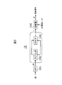
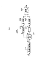
- FIG. 1 is a block diagram of an embodiment of an optical frequency comb generator according to the present invention.
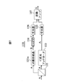
- FIG. 2 is a block diagram of an embodiment of the fceo detection unit in FIG.
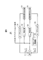
- FIG. 3 is a block diagram of an embodiment of the error signal generator in FIG.
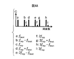
- FIG. 4A is a diagram illustrating a frequency spectrum of a signal output from the differential amplifier.
- FIG. 4B is a diagram illustrating a frequency spectrum of a signal output from the bandpass filter.
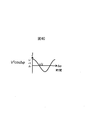
- FIG. 4C is a diagram illustrating a waveform of an error signal generated by the adder.
- FIG. 5 is a frequency spectrum diagram for explaining the operation principle of this embodiment.
- FIG. 6 is a block diagram of a first modification of the offset frequency fceo detection unit.
- FIG. 1 is a block diagram of an embodiment of an optical frequency comb generator according to the present invention.
- FIG. 2 is a block diagram of an embodiment of the fceo detection unit in FIG.
- FIG. 3 is a block diagram
- FIG. 7 is a block diagram of a second modification of the offset frequency fceo detection unit.
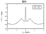
- FIG. 8A is a frequency spectrum diagram of the output signal of the BPF in the error signal detector in the optical frequency comb generator of FIG.
- FIG. 8B is a diagram illustrating a measurement result of a relative Allan deviation of f ceo / f rep .
- FIG. 9 is a block diagram of an application example of the optical frequency comb generator according to the present invention.
- FIG. 10 is a block diagram of an embodiment of the f beat detection unit in FIG.
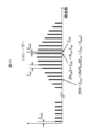
- FIG. 11 is a frequency spectrum diagram of the optical signal f (N) output from the optical comb and the laser oscillation frequency fcw .
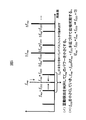
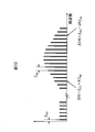
- FIG. 13 is a frequency spectrum diagram of an example of the frequency comb output from the optical comb.
- FIG. 1 shows a block diagram of an embodiment of an optical frequency comb generator according to the present invention.
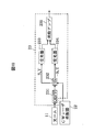
- an optical frequency comb generator 10 of this embodiment includes an optical frequency comb generator (hereinafter simply referred to as “optical comb”) 11, an offset frequency fceo detector 12, and an error signal generator 13.
- the optical frequency comb generator 10 outputs an optical frequency comb that is a pulse laser beam after control that is controlled so that the offset frequency f ceo becomes zero.
- the frequency of the component included in the optical frequency comb and the frequency included in a signal obtained by performing some processing on the optical frequency comb may be referred to as an optical frequency.
- the optical comb 11 is an optical frequency of pulsed laser light including a component having a long wavelength f (N) and a component having a short wavelength f (2N) of the frequency spectrum which is an assembly of the line spectrum shown in FIG. Com A is generated.
- the offset frequency fceo detector 12 significantly attenuates the power of the component having the repetition frequency f rep indicating the frequency interval between adjacent line spectra in the supplied optical frequency comb A using a differential amplifier. A detection signal representing the offset frequency fceo detected in this way is output.
- the error signal generator 13 includes a component having a frequency (f rep ⁇ f ceo ) that is a difference between the repetition frequency and the offset frequency in the optical comb 11 from the detection signal supplied from the offset frequency f ceo detector 12, An error signal for phase-synchronizing with the component having the frequency (f rep + f ceo ) is generated, and the generated error signal is supplied to the optical comb 11 through the loop filter 14.
- FIG. 2 shows a block diagram of an embodiment of the offset frequency fceo detection unit 12 in FIG.
- the offset frequency fceo detection unit 12 includes a nonlinear crystal 121, a beam splitter 122, a variable optical attenuator 123, an optical bandpass filter (OBPF) 124, light receivers 125 and 126, and a differential amplifier 127.
- the nonlinear crystal 121 has, for example, PPLN (periodically poled lithium niobate).
- the nonlinear crystal 121 is supplied with an optical frequency comb A including the frequency component of the long wavelength f (N) and the frequency component of the short wavelength f (2N) of the frequency spectrum shown in FIG.
- the nonlinear crystal 121 generates the second harmonic (frequency 2f (N)) of the frequency component of the long wavelength f (N) and generates the frequency (2f (N) ⁇ f generated by the f-2f interference processing.
- An interference signal including a component having (2N) f ceo ) is output.
- the beam splitter 122 divides the optical signal B (consisting of components having optical frequencies 2f (N), f (N), and f (2N)) supplied from the nonlinear crystal 121 into an optical signal C and an optical signal E. .
- One optical signal C is supplied from the beam splitter 122 to the variable optical attenuator 123, and the other optical signal E is supplied from the beam splitter 122 to the OBPF 124.
- the OBPF 124 cuts out the optical signal F in the optical frequency band in which the second harmonic having the frequency 2f (N) and the short wavelength (frequency f (2N)) component exist simultaneously from the input optical signal E.
- the device 126 is supplied.
- the light receiver 126 is, for example, a photodiode, photoelectrically converts the input optical signal F, and a component having a second harmonic (frequency 2f (N)) in the input signal F and a short wavelength (frequency f (2N)). ) And a component corresponding to an offset frequency f ceo represented by an interference signal and a frequency f rep , 2f rep o , 3f rep ... M times the repetition frequency f rep (m is a natural number of 1 or more).
- a component having a difference frequency between the frequency and the offset frequency f ceo (f rep ⁇ f ceo , 2f rep ⁇ f ceo , 3f rep ⁇ f ceo ,...), And their frequencies And the offset signal f ceo are supplied to the differential amplifier 127 with a first signal comprising a component having a frequency (f rep + f ceo , 2f rep + f ceo , 3f rep + f ceo ,).
- the light receiver 125 is, for example, a photodiode, photoelectrically converts the input optical signal D, and has a frequency f rep , 2f rep o , 3f rep that is m times the repetition frequency f rep (m is a natural number of 1 or more).
- a second signal including a component having... Is supplied to the differential amplifier 127.
- the signal related to the offset frequency f ceo the signal whose frequency is expressed using the offset frequency f ceo , that is, the frequency f ceo , (f rep ⁇ f ceo ), (2f rep ⁇ f ceo ), (3f rep ⁇ f ceo ),...
- the offset frequency f ceo detection unit 12 adjusts the power of the second signal with the variable optical attenuator 123, and the differential amplifier 127 uses the m-fold repetition frequency f rep in the first signal, The signal having 2f rep o , 3f rep ... And the second signal are almost canceled out.
- the differential amplifier 127 outputs a signal G having a frequency spectrum shown in FIG. 4A.
- the signal G is an example of a detection signal. In the signal G of FIG.
- the signal component a is a signal having an offset frequency f ceo and the signal component b is a signal having a frequency (f rep ⁇ f ceo ).
- the signal component c is a signal having a repetitive frequency f rep that is substantially canceled out, the signal component d is a signal having a frequency (f rep + f ceo ), and the signal component e is a frequency (2f rep ⁇ f ceo).
- the signal component f is a signal having a frequency 2f rep that is substantially canceled out
- the signal component g is a signal having a frequency (2f rep + f ceo )
- the signal component h is a frequency (3f rep -F ceo )
- the signal component h is a signal having a frequency 3f rep that is substantially canceled out.
- FIG. 3 shows a block diagram of an embodiment of the error signal generator 13 in FIG.
- the error signal generation unit 13 includes a band pass filter (BPF) 131, a splitter 132, a mixer 133, and an adder 134.
- the BPF 131 has a slightly wider frequency band including the frequency region of (f rep ⁇ f ceo ) to (f rep + f ceo ) in the electric signal G output from the differential amplifier 127 in the offset frequency f ceo detection unit 12. And outputs a signal including the selected frequency band.
- the BPF 131 selects and outputs the signal components b, c, and d in the signal G of the frequency spectrum shown in FIG. 4A, and greatly suppresses the other signal components to obtain the frequency spectrum shown in FIG. 4B.
- the signal H is output.
- the splitter 132 bisects the input signal H and supplies it to the mixer 133.
- the mixer 133 multiplies the supplied signals to generate a square signal of the input signal H, and outputs the square signal.
- the mixer 133 since the input signal H is sufficiently low level and can be ignored except for the signal components b and d, the mixer 133 has the signal component b of the frequency (f rep ⁇ f ceo ) and the frequency ( A square signal I represented by the following equation, which is composed of the signal component d of f rep + f ceo ), is output.
- ⁇ ⁇ Vcos [2 ⁇ (f rep -f ceo ) t] + Vcos [2 ⁇ (f rep + f ceo ) t + ⁇ ] ⁇ 2 (5)
- ⁇ indicates the phase difference between the signal components b and d.
- the adder 134 adds a predetermined DC voltage ⁇ V 2 to the square signal I supplied from the mixer 133 to generate a signal J after addition, and uses the signal J as an error signal through the loop filter 14 of FIG. Feedback output to the comb 11.
- This error signal J is a basis for a phase error signal between a component having a frequency (f rep ⁇ f ceo ) and a component having a frequency (f rep + f ceo ).
- the phase difference generated by the difference between the two electric path lengths between the splitter 132 and the mixer 133 changes the amplitude and the positive / negative polarity of the error signal J. However, an appropriate electric path length (in many cases, the same electric path length). By selecting, the maximum amplitude and desired polarity can be obtained.
- the current of the pumping laser inside the optical comb 11 is controlled by the error signal J, so that the offset frequency f ceo in the output optical frequency comb is the frequency (f rep ⁇ f ceo) and the frequency of the signal component d (f rep + f ceo) is variably controlled so as to approach.
- (f rep ⁇ f ceo ) (f rep + f ceo ).
- the adder 134 removes high-frequency components not related to phase synchronization in the equation (6) from the square signal I with a low-pass filter (not shown), and then adds the predetermined DC voltage ⁇ V 2 to the square signal I after removal.
- an error signal J having a waveform shown in FIG. 4C represented by V 2 cos ⁇ is generated.
- the only new function required is a simple differential detection function, and the optical frequency comb generator does not need to add a complicated function and limits the wavelength band of the optical frequency comb. It is possible to have a simple configuration that is not required. Also, in this method, the offset frequency f ceo of the light that has not been subjected to the broadband processing of the light source portion of the original optical comb 11 becomes zero, so that the optical frequency comb generator performs the broadband processing from the light source portion of the optical comb 11. It is also possible to use light that has not been lighted by making it broadband once. Furthermore, the optical frequency comb generator can also use an optical frequency comb with a sufficiently wide band generated to detect the offset frequency f ceo as it is.
- variable attenuator 123 and the differential amplifier 127 have the frequency (f rep ⁇ f ceo ) and the power of the component of (f rep + f ceo ), the power of the component of the repetition frequency f rep is made relatively small.
- FIG. 6 shows a block diagram of a first modification of the offset frequency fceo detection unit 12.
- the offset frequency fceo detection unit 12 ⁇ / b> A according to the first modification includes a polarization beam splitter 128 instead of the beam splitter 122, and a variable optical attenuator or polarizer 129 instead of the variable optical attenuator 123.
- the second harmonic (frequency 2f (N)) of the optical signal B (consisting of components having optical frequencies 2f (N), f (N), f (2N)) obtained by the nonlinear crystal 121 is used.
- the polarization beam splitter 128 splits the optical signal B into two. Then, an optical frequency comb A including a component having optical frequencies f (N) and f (2N) is output to one optical path (that is, an optical signal composed of a fundamental wave component), and a fundamental wave component is output to the other optical path. And the second harmonic are output as an optical signal E (that is, the same as the optical signal B).
- the polarization of the light separated by the polarization beam splitter 128 becomes linearly polarized light. Therefore, when a polarizer is used as the variable optical attenuator or polarizer 129, the offset frequency fceo detector 12A detects the same as when the variable optical attenuator is used by rotating the transmission axis of the polarizer. It is possible to adjust the power of signal components having frequencies f rep , 2f rep o , 3f rep ... M times the repetition frequency f rep (m is a natural number of 1 or more).
- the light receiver 125 supplies a second signal composed of signal components having frequencies f rep , 2f rep o , 3f rep ... M times the repetition frequency f rep to the differential amplifier 127.
- FIG. 7 shows a block diagram of a second modification of the offset frequency fceo detection unit 12.
- the offset frequency fceo detection unit 12B of the second modified example supplies the optical frequency comb A from the optical comb 11 to the nonlinear crystal 121a and the variable optical attenuator 123 by branching the optical frequency comb A from the beam splitter 122.
- the nonlinear crystal 121a generates the second harmonic (frequency 2f (N)) of the frequency component of the long wavelength f (N) based on the optical frequency comb A supplied from the beam splitter 122, and the second harmonic ( The frequency 2f (N)) is output together with the components having the input frequencies f (N) and f (2N).
- the optical signal B output from the nonlinear crystal 121a includes the second harmonic (frequency 2f (N)) together with the components having the input frequencies f (N) and f (2N).
- the nonlinear crystal 121a has PPLN like the nonlinear crystal 121, for example.
- the OBPF 124 generates an optical signal F in an optical frequency band including both the second harmonic (frequency 2f (N)) and the short wavelength f (2N) in the optical signal B supplied from the nonlinear crystal 121a. It is cut out from the optical signal B and supplied to the light receiver 126.
- the frequency spectrum figure of the output signal of BPF131 in error signal detection part 13 at the time is shown.
- the output signal (in-loop beat signal) of the BPF 131 shows a peak at the repetition frequency f rep . Therefore, it is strongly suggested that the offset frequency f ceo is zero due to phase synchronization (clear evidence will be described later).
- the S / N of the coherent peak was about 84 dB ⁇ Hz, which was the same as in the normal case where the offset frequency f ceo was phase-synchronized with the synthesizer reference signal.
- the beat signal (frequency f in-loop ) of the phase-synchronized offset frequency f ceo and the repetition frequency f directly detected by another port are used.
- the frequency of rep was measured with a counter, and the relative Allan deviation of f in-loop / f rep was calculated.
- f ceo 0, f in-loop matches f rep .
- FIG. 8B shows the measurement result of the relative Allan deviation of f in-loop / f rep .
- the relative allan deviation of the counter limit was obtained, and the phase synchronization performance of this embodiment was high in combination with the in-loop beat spectrum, and it was confirmed that it was equivalent to the normal phase synchronization of the offset frequency fceo .
- optical frequency comb generator of this embodiment shows an example in which the optical frequency comb generator of this embodiment is applied to an optical frequency divider.
- the optical frequency comb generator is useful not only in optical frequency division but also in many fields including the application of attosecond optical pulses for controlling the carrier envelope phase.
- the application of the apparatus is not limited to the optical frequency divider.
- FIG. 9 shows a block diagram of an application example of the optical frequency comb generator according to the present invention.
- the optical frequency divider 20 which is this application example is configured by combining the optical frequency comb generator 10 shown in FIG. 1 with a beat optical frequency zero control circuit for controlling the beat optical frequency f beat to zero.
- the same components as those in FIG. 1 are denoted by the same reference numerals, and the description thereof is omitted as appropriate.
- the optical comb 11 is controlled so that the offset frequency f ceo of the generated optical frequency comb is zero by the first feedback loop including the f ceo detection unit 12, the error signal generation unit 13, and the loop filter 14.
- the optical comb 11 is based on the oscillation frequency f cw of CW laser oscillator 22, generates the (N / N cw) dividing represented by f cw optical frequency comb f (N).
- N is an arbitrary natural number
- N cw is a constant value corresponding to a desired frequency division ratio.
- the f beat detector 23 is supplied with the optical frequency comb from the optical comb 11 and the CW laser signal from the CW laser oscillator 22.
- the f beat detection unit 23 photoelectrically converts an optical signal including an interference signal between the optical frequency comb and the CW laser signal, a component corresponding to the beat frequency f beat , and m times the repetition frequency f rep (m is 1 or more).
- the error signal detection unit 24 includes a component having a frequency (f rep ⁇ f beat ) of the difference between the repetition frequency and the beat frequency in the optical comb 11 and the sum frequency ( An error signal for phase-synchronizing with the component having f rep + f beat ) is generated, and the generated error signal is supplied to the optical comb 11 through the loop filter 25.
- FIG. 10 shows a block diagram of an embodiment of the f beat detection unit 23 in FIG.
- the f beat detection unit 23 includes an optical bandpass filter (OBPF) 231, a 1: 1 beam splitter (BS) 232, light receivers 233 and 234, and a differential amplifier 235.
- the 1: 1 beam splitter (BS) 232 may be a half mirror.
- the OBPF 231 is a narrow optical frequency region (for example, ⁇ several) centered on an optical signal having a frequency f (N cw ) closest to the oscillation frequency f cw of the CW laser signal among the optical signals of the optical frequency comb output from the optical comb 11.
- the optical signal within 1000 f rep is selected and output.
- FIG. 11 shows the frequency spectrum of the optical signal in the f beat detector 23.
- the beat frequency f beat between the frequency f cw is expressed by the following equation.
- the repetition frequency f rep is expressed by the following equation.
- f rep (f cw ⁇ f ceo ⁇ f beat ) / N cw (9) Therefore, the frequency f (N) in the optical frequency comb is expressed by the following equation by substituting the equation (9) into the equation (1).
- f (N) f ceo + (N / N cw ) (f cw ⁇ f ceo ⁇ f beat ) (10)
- the 1: 1 beam splitter (BS) 232 in FIG. 10 outputs an optical signal in a narrow optical frequency region centered on the frequency f (N cw ) of the optical signal from the OBPF 231 and the CW laser signal from the CW laser oscillator 22. Synthesize and branch into two for output.
- An optical signal including beat signals S and T is output on one optical path, and an optical signal including beat signals -S and T is output on the other optical path.
- the beat signal -S is a phase inversion signal of the beat signal S.
- the light receiver 233 photoelectrically converts an optical signal including the beat signals S and T, and corresponds to the beat signal S, f beat , (f rep ⁇ f beat ), (f rep + f beat ), (2f rep ⁇ f Outputs a signal composed of a component having a frequency of beat ),... and a component having a frequency of f rep , 2f rep , 3f rep,. To do.
- This output signal is input to the differential amplifier 235 as a first signal.
- the light receiver 234 photoelectrically converts an optical signal including the beat signals -S and T, and corresponds to the beat signal -S, f beat , (f rep -f beat ), (f rep + f beat ), ( 2f rep -f beat ),... And a component corresponding to the beat signal T and having a frequency of f rep , 2f rep , 3f rep,. Is output.
- This output signal is input to the differential amplifier 235 as a second signal.
- Each of the light receiver 233 and the light receiver 234 can be, for example, a photodiode.
- the differential amplifier 235 differentially amplifies the first and second signals to significantly suppress the m-fold repetition frequencies f rep , 2f rep o , 3f rep ... And f beat , ( The electrical signal of the component having the frequency consisting of f rep ⁇ f beat ), (f rep + f beat ), (2f rep ⁇ f beat ),... is output to the error signal generator 24.
- the error signal generation unit 24 includes a band pass filter, a square circuit, and an adder. First, (f rep ⁇ f beat ) to (f rep + f) in the electric signal supplied from the differential amplifier 235 by the band pass filter. A signal having a frequency band slightly wider than that including the frequency range of beat ) is selected.
- the signal output from the bandpass filter is substantially the signal of the frequency (f rep ⁇ f beat ) and the frequency (f rep + f beat). ) Signal.
- the square circuit outputs a square signal U expressed by the following equation from the frequency (f rep ⁇ f beat ) signal and the frequency (f rep + f beat ) signal supplied from the bandpass filter.
- ⁇ ⁇ Vcos [2 ⁇ (f rep -f beat ) t] + Vcos [2 ⁇ (f rep + f beat ) t + ⁇ ] ⁇ 2 (11)
- ⁇ represents a phase difference between the signal of the above frequency (f rep ⁇ f beat ) and the signal of the frequency (f rep + f beat ).
- the adder in the error detection unit 24 adds a predetermined DC voltage ⁇ V 2 to the square signal U to generate an error signal, and supplies this error signal to the optical comb 11.
- the optical comb 11 causes the f beat control actuator such as an electro-optic modulator or a piezo element in the internal laser resonator to transmit the optical frequency (f rep in the frequency comb output from the optical comb 11.
- -F beat ) and (f rep + f beat ) are controlled so as to be close to each other, and the frequency (f rep -f beat ) signal and the frequency (f rep + f beat ) signal are phase-synchronized.
- the adder in the error detector 24 removes a high-frequency component not related to phase synchronization in the equation (12) from the square signal U with a low-pass filter (not shown), and then adds the predetermined DC to the square signal U after the removal.
- a low-pass filter not shown
- V 2 cos ⁇ an error signal having the same waveform as the waveform shown in FIG. 4C represented by V 2 cos ⁇
- the generated error signal is output to the optical comb 11 through the loop filter 25.
- the optical comb 11 generates an optical frequency comb in which the beat frequency f beat is controlled to be zero, and outputs the optical frequency comb to the output terminal 26 in FIG.
- the optical frequency divider 20 controls the offset frequency f ceo of the optical frequency comb to zero by the first feedback loop including the f ceo detection unit 12, the error signal generation unit 13, and the loop filter 14.
- the beat frequency f beat is controlled to zero by the second feedback loop including the f beat detection unit 23, the error signal generation unit 24, and the loop filter 25.
- the optical frequency divider 20 makes the offset frequency f ceo of the optical comb 21 zero by the first feedback loop circuit 27 having the above-described f ceo detection unit 12, error signal generation unit 13, and loop filter 14.
- the second feedback loop circuit 28 having the f beat detection unit 23, the error signal generation unit 24, and the loop filter 25 is used to control the reference laser frequency and the optical frequency comb from the reference laser oscillator 41 of the optical comb 21.
- the beat frequency f beat between optical signals having a frequency closest to the reference laser frequency is controlled to zero.
- the optical frequency divider 30 having an offset frequency locks the offset frequency of the optical comb 31 to 29.9 MHz by a known first phase-locked loop (PLL) circuit 32 and a known second PLL circuit. 33 controls the beat frequency between the reference laser frequency from the reference laser oscillator 41 of the optical comb 31 and the optical signal having the frequency closest to the reference laser frequency in the optical frequency comb to 29.9 MHz.
- PLL phase-locked loop
- an optical bandpass filter (OBPF) 42 selects an optical signal having a wavelength of 1020 nm and a wavelength region in the vicinity thereof.
- the OBPF 43 selects an optical signal having a wavelength of 1020 nm and a wavelength region in the vicinity thereof.
- the repetition frequency f rep in each frequency comb emitted from the optical combs 21 and 31 is set equal.
- the counter 44 counts the frequency of the two out-of-loop beat signals selected by the OBPFs 42 and 43, respectively.
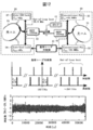
- the graph shown second from the top in FIG. 12 shows the frequency spectrum of the optical signal from the optical comb 21, and the graph shown third from the top in FIG. 12 shows the frequency spectrum of the optical signal from the optical comb 31.
- the waveform shown at the bottom of FIG. 12 shows the measured out-of-loop beat frequency and the relative Allan deviation with respect to the optical frequency of 200 THz.
Landscapes
- Physics & Mathematics (AREA)
- Nonlinear Science (AREA)
- Optics & Photonics (AREA)
- General Physics & Mathematics (AREA)
- Electromagnetism (AREA)
- Engineering & Computer Science (AREA)
- Plasma & Fusion (AREA)
- Optical Modulation, Optical Deflection, Nonlinear Optics, Optical Demodulation, Optical Logic Elements (AREA)
Abstract
光周波数コム発生器11は、一定の繰り返し周波数frepの複数の線スペクトルの集合体で表されるパルスレーザ光である光周波数コムAを発生する。オフセット周波数fceo検出部12は、供給された光周波数コムAの隣接する線スペクトラム間の周波数間隔を示す繰り返し周波数frepを持つ成分のパワーを差動アンプを用いて大幅に減衰させて検出したオフセット周波数fceoを表す検出信号を出力する。誤差信号生成部13は、オフセット周波数fceo検出部12から供給される検出信号から、光周波数コム発生器11から発する光周波数コム中の繰り返し周波数とオフセット周波数との差の周波数 (frep-fceo)を持つ成分と、和の周波数(frep+fceo)を持つ成分とを位相同期するための誤差信号を生成し、ループフィルタ14を通して光周波数コム発生器11に供給する。
Description
本発明は、光周波数コム発生装置に関し、特にオフセット周波数fceoゼロの光周波数コムを発生する光周波数コム発生装置に関する。
図13に示されるように、1本1本は細い周波数スペクトラムが一定の繰り返し周波数frepの周波数間隔で櫛歯状に並ぶ複数の線スペクトルの集合体で表されるパルスレーザ光である光周波数コムが、1オクターブ以上の帯域にわたって存在する場合、光周波数コムの周波数スペクトラム1300は、長波長(低周波数f(N))を持つ成分と短波長(高周波数f(2N))を持つ成分とを同時に含む。長波長(低周波数f(N))を持つ成分及び短波長(高周波数f(2N))を持つ成分は、オフセット周波数fceoだけオフセットされているため、それぞれの成分の周波数は、次式で表される。
f(N)=N×frep+fceo (1)
f(2N)=2N×frep+fceo (2)
ただし、上式中Nは0又は自然数であり、モード次数を示す。また、オフセット周波数fceoは正式にはキャリアエンベロープオフセット周波数と呼ばれる(ただし、本明細書では便宜上「オフセット周波数」と略す)。また、オフセット周波数fceoと繰り返し周波数frepとの間には、次の不等式が成立する。
0≦fceo≦frep (3)
f(N)=N×frep+fceo (1)
f(2N)=2N×frep+fceo (2)
ただし、上式中Nは0又は自然数であり、モード次数を示す。また、オフセット周波数fceoは正式にはキャリアエンベロープオフセット周波数と呼ばれる(ただし、本明細書では便宜上「オフセット周波数」と略す)。また、オフセット周波数fceoと繰り返し周波数frepとの間には、次の不等式が成立する。
0≦fceo≦frep (3)
この光周波数コムのオフセット周波数fceoの制御は、精密周波数メトロロジ及び超高速物理だけでなく、化学及び天文においても重要な基盤技術である。特に、fceo=0に制御された光周波数コムは、光周波数分周、または、キャリアエンベロープ位相を制御するアト秒光パルスの応用などをはじめ、多くの分野において有用である。光周波数コムのオフセット周波数fceoは、f-2f干渉計によって長波長成分の第2高調波(周波数2f(N))を持つ光と短波長(高周波数f(2N))を持つ光とを干渉させて得られる干渉信号において、第2高調波(周波数2f(N))と短波長(高周波数f(2N))を持つ成分とのビート信号として検出される。このf-2f干渉計では、周波数が安定なオフセット周波数fceoを得るため、光周波数コムのオフセット周波数fceoと基準マイクロ波信号との位相弁別が行われ、光周波数コムのオフセット周波数fceoと基準マイクロ波信号間の位相差が一定になるように位相同期することが一般的に行われる。しかし、ゼロ周波数(直流)には位相が存在せず位相弁別は不可能であるため、そのままではオフセット周波数fceoをゼロに安定化することができない。
そこで、従来より、オフセット周波数fceoがゼロとなる光周波数コムを発生する光周波数コム発生装置が提案されている(例えば、非特許文献1及び2、特許文献1参照)。非特許文献1には、オフセット周波数fceoをゼロとなる光周波数コムを発生する装置が開示されている。この装置は、音響光学変調器(AOM)により変調周波数fAOMだけ周波数シフトした光周波数コムからf-2f干渉計を用いて周波数(fceo+fAOM)を検出し、このシフトした周波数を持つ信号を周波数fAOMに位相同期することで、次式に従ってオフセット周波数fceoをゼロとする。
fceo+fAOM=fAOM (4)
fceo+fAOM=fAOM (4)
また、非特許文献2及び特許文献1には、広帯域化した光周波数コムに含まれる低周波数成分(周波数:fceo+n1frep)と高周波数成分(周波数:fceo+n2frep)とを、非線形光学結晶を用いた差周波発生器(DFG)に供給し、それらの差周波数成分(周波数:(n2-n1)frep)を生成することで、DFGからオフセット周波数fceoをゼロとした光周波数コムを出力させる装置が開示されている。
Rausch et al.,Opt.Express.17,20282,(2009)
論文 Krauss et al.,Opt.Lett.36,540(2011)
しかしながら、AOMを用いる従来の光周波数コム発生装置では、高価なAOMが必要で装置全体として高価な構成となり、また、0次光の混入などによって制御に用いる信号のS/Nが低下するという課題がある。一方、DFGを用いる従来の光周波数コム発生装置では、DFGから得られるオフセット周波数fceoをゼロとした光周波数コムの帯域が狭いため、得られた光周波数コムに対してもう一度広帯域化処理(以下、単に「再広帯域化」と略す)を必要とするという課題がある。
本発明は以上の点に鑑みなされたもので、簡単で、しかも再広帯域化が不要な構成によりオフセット周波数fceoをゼロとした光周波数コムを発生する光周波数コム発生装置を提供することを目的とする。
上記の目的を達成するため、本発明の光周波数コム発生装置は、オフセット周波数fceoだけオフセットされ、かつ、一定の繰り返し周波数frepの周波数間隔で櫛歯状に並ぶ複数の線スペクトルの集合体で表されるパルスレーザ光である光周波数コムを発生する光周波数コム発生器と、光周波数コム発生器から出力された光周波数コムからオフセット周波数fceoを表す検出信号を生成して、その検出信号を出力する検出部と、その検出信号から周波数(frep-fceo)を持つ成分と周波数(frep+fceo)を持つ成分とを位相同期させるための誤差信号を生成し、その誤差信号を光周波数コム発生器にフィードバックして、光周波数コム発生器から出力される光周波数コム中のオフセット周波数fceoをゼロに可変制御する誤差信号検出部と、を有する。
本発明による光周波数コム発生装置は、簡単で、しかも再広帯域化が不要な構成によりオフセット周波数fceoをゼロとした光周波数コムを発生することができる。
次に、本発明の実施形態について図面を参照して説明する。
図1は、本発明に係る光周波数コム発生装置の一実施形態のブロック図を示す。同図に示すように、本実施形態の光周波数コム発生装置10は、光周波数コム発生器(以下、単に「光コム」と略す)11、オフセット周波数fceo検出部12、誤差信号生成部13、ループフィルタ14を含むフィードバックループ構成を有する。そして光周波数コム発生装置10は、光コム11からオフセット周波数fceoがゼロとなるように制御された制御後のパルスレーザ光である光周波数コムを出力する。
なお、以下では、光周波数コムに含まれる成分の周波数、及び、光周波数コムに対する何らかの処理を行って得られる信号に含まれる周波数を、光周波数と呼ぶことがある。
図1は、本発明に係る光周波数コム発生装置の一実施形態のブロック図を示す。同図に示すように、本実施形態の光周波数コム発生装置10は、光周波数コム発生器(以下、単に「光コム」と略す)11、オフセット周波数fceo検出部12、誤差信号生成部13、ループフィルタ14を含むフィードバックループ構成を有する。そして光周波数コム発生装置10は、光コム11からオフセット周波数fceoがゼロとなるように制御された制御後のパルスレーザ光である光周波数コムを出力する。
なお、以下では、光周波数コムに含まれる成分の周波数、及び、光周波数コムに対する何らかの処理を行って得られる信号に含まれる周波数を、光周波数と呼ぶことがある。
光コム11は、前述した図13に示した線スペクトラムの集合体である周波数スペクトラムの長波長f(N)を持つ成分と短波長f(2N)を持つ成分とを含むパルスレーザ光の光周波数コムAを発生する。オフセット周波数fceo検出部12は、供給された光周波数コムAのうちの互いに隣接する線スペクトラム間の周波数間隔を示す繰り返し周波数frepを持つ成分のパワーを差動アンプを用いて大幅に減衰させて検出したオフセット周波数fceoなどを表す検出信号を出力する。誤差信号生成部13は、オフセット周波数fceo検出部12から供給される検出信号から光コム11中の繰り返し周波数とオフセット周波数との差の周波数(frep-fceo)を持つ成分と、和の周波数(frep+fceo)を持つ成分とを位相同期するための誤差信号を生成し、生成した誤差信号をループフィルタ14を通して光コム11に供給する。
次に、図1中の各ブロックの構成について更に詳細に説明する。図2は、図1中のオフセット周波数fceo検出部12の一実施形態のブロック図を示す。図2において、オフセット周波数fceo検出部12は、非線形結晶121、ビームスプリッタ122、可変光アッテネータ123、光バンドパスフィルタ(OBPF)124、受光器125及び126、差動アンプ127を有する。非線形結晶121は、例えばPPLN(periodically poled lithium niobate)を有する。非線形結晶121には、図13に示した周波数スペクトラムの長波長f(N)の周波数成分と短波長f(2N)の周波数成分とを含む光周波数コムAが供給される。そして非線形結晶121は、長波長f(N)の周波数成分の第2高調波(周波数2f(N))を発生し、f-2f干渉処理されることで発生する周波数(2f(N)-f(2N)=fceo)を持つ成分を含む干渉信号を出力する。
ビームスプリッタ122は、非線形結晶121から供給された光信号B(光周波数2f(N)、f(N)、f(2N)を持つ成分からなる)を光信号C及び光信号Eに2分割する。一方の光信号Cは、ビームスプリッタ122から可変光アッテネータ123に供給され、他方の光信号Eは、ビームスプリッタ122からOBPF124に供給される。OBPF124は、入力された光信号Eから、周波数2f(N)を持つ第2高調波と短波長(周波数f(2N))の成分とが同時に存在する光周波数帯域の光信号Fを切り出して受光器126に供給する。受光器126は、例えば、フォトダイオードであり、入力光信号Fを光電変換して、入力信号F中の第2高調波(周波数2f(N))を持つ成分と短波長(周波数f(2N))を持つ成分との干渉信号により表されるオフセット周波数fceoに相当する成分と、繰り返し周波数frepのm倍(mは1以上の自然数)の周波数frep、2frep o、3frep・・・を持つ成分と、それらの周波数とオフセット周波数fceoとの差の周波数(frep-fceo、2frep-fceo、3frep-fceo、・・・)を持つ成分と、それらの周波数とオフセット周波数fceoとの和の周波数(frep+fceo、2frep+fceo、3frep+fceo、・・・)を持つ成分とからなる第1の信号を差動アンプ127に供給する。
一方、受光器125は、例えば、フォトダイオードであり、入力光信号Dを光電変換して、繰り返し周波数frepのm倍(mは1以上の自然数)の周波数frep、2frep o、3frep・・・を持つ成分を含む第2の信号を差動アンプ127に供給する。ここで、光信号DはOBPFを通していないので、オフセット周波数fceo関連の信号(周波数がオフセット周波数fceoを用いて表される信号、すなわち、周波数fceo、(frep-fceo)、(2frep-fceo)、(3frep-fceo)、...、(frep+fceo)、(2frep+fceo)、(3frep+fceo)、...などの信号)に対して繰り返し周波数frepを持つ信号のパワーが圧倒的に大きい。そこで、本実施形態によるオフセット周波数fceo検出部12は、第2の信号のパワーを可変光アッテネータ123で調整し、差動アンプ127において、第1の信号中のm倍の繰り返し周波数frep、2frep o、3frep・・・を持つ信号と第2の信号とがほぼ相殺除去されるようにしている。これにより、差動アンプ127は、図4Aに示す周波数スペクトラムの信号Gを出力する。ここで、信号Gは、検出信号の一例であり、図4Aの信号G中、信号成分aはオフセット周波数fceoを持つ信号であり、信号成分bは周波数(frep-fceo)を持つ信号であり、信号成分cはほぼ相殺除去された繰り返し周波数frepを持つ信号であり、信号成分dは周波数(frep+fceo)を持つ信号であり、信号成分eは周波数(2frep-fceo)を持つ信号であり、信号成分fはほぼ相殺除去された周波数2frepを持つ信号であり、信号成分gは周波数(2frep+fceo)を持つ信号であり、信号成分hは周波数(3frep-fceo)を持つ信号であり、信号成分hはほぼ相殺除去された周波数3frepを持つ信号である。
次に、図1中の誤差信号生成部13の構成及び動作について説明する。図3は、図1中の誤差信号生成部13の一実施形態のブロック図を示す。図3において、誤差信号生成部13は、バンドパスフィルタ(BPF)131、スプリッタ132、ミキサ133及び加算器134を有する。BPF131は、オフセット周波数fceo検出部12内の差動アンプ127から出力された電気信号G中の(frep-fceo)~(frep+fceo)の周波数領域を含むそれより若干広い周波数帯域を選択し、選択した周波数帯域を含む信号を出力する。したがって、BPF131は図4Aに示した周波数スペクトラムの信号G中の信号成分b、c及びdを選択して出力し、それ以外の信号成分を大幅に抑圧して、図4Bに示す周波数スぺトラムの信号Hを出力する。
スプリッタ132は、入力信号Hを二分してミキサ133にそれぞれ供給する。ミキサ133は、供給された信号同士を乗じることで、入力信号Hの二乗信号を生成し、その二乗信号を出力する。ここで、入力信号Hは図4Bに示したように、信号成分b及びd以外は十分低レベルであり無視できるので、ミキサ133は、周波数(frep-fceo)の信号成分b及び周波数(frep+fceo)の信号成分dからなる次式で示す二乗信号Iを出力する。
I={Vcos[2π(frep-fceo)t]+Vcos[2π(frep+fceo)t+Δφ]}2 (5)
ただし、上式中、Δφは上記信号成分b及びdの位相差を示す。
I={Vcos[2π(frep-fceo)t]+Vcos[2π(frep+fceo)t+Δφ]}2 (5)
ただし、上式中、Δφは上記信号成分b及びdの位相差を示す。
加算器134はミキサ133から供給された二乗信号Iに、所定の直流電圧-V2を加算して加算後の信号Jを生成し、その信号Jを誤差信号として図1のループフィルタ14を通して光コム11にフィードバック出力する。この誤差信号Jは、周波数(frep-fceo)を持つ成分と周波数(frep+fceo)を持つ成分間の位相の誤差信号の基となる。スプリッタ132とミキサ133間の2本の電気路長差により発生する位相差により、この誤差信号Jの振幅と正負の極性が変化するが、適切な電気路長(多くの場合同じ電気路長)を選ぶことで最大の振幅かつ所望の極性が得られる。光コム11内部の例えば励起レーザの電流が誤差信号Jにより制御されることで、出力される光周波数コムにおけるオフセット周波数fceoが、(5)式中の信号成分bの周波数(frep-fceo)と信号成分dの周波数(frep+fceo)とが近づくように可変制御される。そして、両信号成分b及びdを位相同期することにより、(frep-fceo)=(frep+fceo)となる。この結果、(5)式の二乗信号Iは次式で示されるようになる。
I=V2+V2cosΔφ+(位相同期に関係ない高周波成分) (6)
I=V2+V2cosΔφ+(位相同期に関係ない高周波成分) (6)
加算器134は、二乗信号Iから(6)式中の位相同期に関係ない高周波成分を図示しないローバスフィルタで除去した後、除去後の二乗信号Iに上記所定の直流電圧-V2を加算することで、V2cosΔφで表される図4Cに示す波形の誤差信号Jを生成する。このように、(frep-fceo)=(frep+fceo)に近づけるようにオフセット周波数fceoが制御されて信号成分b及びdを位相同期することにより、光コム11はオフセット周波数fceoがゼロに制御された光周波数コムを発生して図1の出力端子15へ出力する。
本実施形態によれば、新たに必要となる機能は簡単な差動検出機能のみであり、光周波数コム発生装置は、複雑な機能を加えなくてよく、かつ、光周波数コムの波長帯域を制限することがない簡単な構成とすることができる。また、この手法ではもともとの光コム11の光源部の広帯域化処理されていない光のオフセット周波数fceoがゼロになるので、光周波数コム発生装置は、光コム11の光源部からの広帯域化処理されていない光を一度だけ広帯域化することで使用することも可能である。さらに、光周波数コム発生装置は、オフセット周波数fceoを検出するために発生させた、十分広帯域な光周波数コムをそのまま使用することも可能である。
本実施形態の動作原理について、図5と共に更に説明する。本実施形態では、図5に示す周波数スペクトラムの光周波数コムのうち、まず、図5に(イ)で示すように、図2の可変アッテネータ123及び差動アンプ127は、周波数(frep-fceo)の成分及び(frep+fceo)の成分のパワーに比して、繰り返し周波数frepの成分のパワーを相対的に小さくする。その後、前述した図1のオフセット周波数fceo検出部12、誤差信号生成部13、ループフィルタ14及び光コム11のフィードバックループは、図5に(ロ)で示すように、オフセット周波数fceoを可変制御して、周波数(frep-fceo)と周波数(frep+fceo)とを近づけてから信号成分b及びdを位相同期する。その結果、周波数(frep-fceo)と周波数(frep+fceo)とがロックされて下記の関係が成立する。
(frep-fceo)=(frep+fceo) (7)
したがって、オフセット周波数fceoがゼロになる。
(frep-fceo)=(frep+fceo) (7)
したがって、オフセット周波数fceoがゼロになる。
次に、オフセット周波数fceo検出部12の変形例について説明する。図6は、オフセット周波数fceo検出部12の第1変形例のブロック図を示す。同図中、図2と同一構成部分には同一符号を付し、その説明を省略する。図6において、第1変形例のオフセット周波数fceo検出部12Aは、ビームスプリッタ122の代わりに偏光ビームスプリッタ128を有し、可変光アッテネータ123の代わりに可変光アッテネータ又は偏光子129を有する。本変形例では、非線形結晶121により得られる光信号B(光周波数2f(N)、f(N)、f(2N)を持つ成分からなる)のうち、第2高調波(周波数2f(N))では偏光が揃っているので、偏光ビームスプリッタ128は光信号Bを2分岐する。そして、一方の光路には光周波数f(N)、f(2N)を持つ成分を含む光周波数コムA(すなわち、基本波成分からなる光信号)が出力され、他方の光路には基本波成分と第2高調波とからなる光信号E(すなわち、光信号Bと同じ)が出力される。
偏光ビームスプリッタ128で分離した光の偏光は直線偏光になる。そのため、可変光アッテネータ又は偏光子129として偏光子が用いられる場合は、偏光子の透過軸を回転させることで、可変光アッテネータが用いられる場合と同様に、オフセット周波数fceo検出部12Aは、検出される繰り返し周波数frepのm倍(mは1以上の自然数)の周波数frep、2frep o、3frep・・・を持つ信号成分のパワーを調整することができる。受光器125は繰り返し周波数frepのm倍の周波数frep、2frep o、3frep・・・を持つ信号成分からなる第2の信号を差動アンプ127に供給する。
図7は、オフセット周波数fceo検出部12の第2変形例のブロック図を示す。同図中、図2と同一構成部分には同一符号を付し、その説明を省略する。図7において、第2変形例のオフセット周波数fceo検出部12Bは、光コム11からの光周波数コムAをビームスプリッタ122により2分岐して非線形結晶121a及び可変光アッテネータ123へ供給する。非線形結晶121aは、ビームスプリッタ122から供給された光周波数コムAに基づき、長波長f(N)の周波数成分の第2高調波(周波数2f(N))を発生し、その第2高調波(周波数2f(N))を入力周波数f(N)及びf(2N)を持つ成分と共に出力する。すなわち、非線形結晶121aから出力される光信号Bは、入力周波数f(N)及びf(2N)を持つ成分とともに、第2高調波(周波数2f(N))を含む。なお、非線形結晶121aは、例えば、非線形結晶121と同様に、PPLNを有する。OBPF124は、非線形結晶121aから供給される光信号B中の第2高調波(周波数2f(N))と短波長f(2N)の周波数成分とがともに含まれる光周波数帯域の光信号Fを、光信号Bから切り出して受光器126に供給する。
次に、本実施形態の実験結果について説明する。図8Aは、本実施形態の光周波数コム発生装置10が、信号成分b及びdが位相同期するよう動作し、かつ、(frep-fceo)=(frep+fceo)が成立しているときの、誤差信号検出部13中のBPF131の出力信号の周波数スペクトル図を示す。図8Aに示すように、BPF131の出力信号(インループビート信号)は繰り返し周波数frepにおいてピークを示す。そのため、位相同期によりオフセット周波数fceoがゼロであることが強く示唆されている(明確な証拠については後述)。コヒーレントピークのS/Nは約84dB・Hzで、オフセット周波数fceoがシンセサイザーの基準信号に位相同期される通常の場合と同様であった。
また、本実施形態の位相同期の影響と安定度を調べるため、位相同期されたオフセット周波数fceoのインループでのビート信号(周波数fin-loop)と別のポートで直接検出した繰り返し周波数frepをそれぞれカウンタで周波数計測し、fin-loop/frepの相対アラン偏差を計算した。fceo=0のとき、fin-loopはfrepと一致する。図8Bは、fin-loop/frepの相対アラン偏差の測定結果を示す。カウンタリミットの相対アラン偏差が得られており、インループビートスペクトルと合わせて本実施形態の位相同期の性能は高く、オフセット周波数fceoの通常の位相同期と同等であることが確認できた。
次に、本実施形態の光周波数コム発生装置の応用例について説明する。以下説明する応用例は、本実施形態の光周波数コム発生装置を光周波数分周器に応用した例を示す。ただし、前述したように、光周波数コム発生装置は、光周波数分周だけでなく、キャリアエンベロープ位相を制御するアト秒光パルスの応用などをはじめ、多くの分野において有用であり、光周波数コム発生装置の用途は、光周波数分周器に限定されるものではない。
図9は、本発明に係る光周波数コム発生装置の一応用例のブロック図を示す。この応用例である光周波数分周器20は、図1に示した光周波数コム発生装置10にビート光周波数fbeatをゼロに制御するビート光周波数ゼロ制御回路を組み合わせて構成される。図9において、図1と同一構成部分には同一符号を付し、その説明を適宜省略する。
図9において、光コム11は発生する光周波数コムのオフセット周波数fceoが、fceo検出部12、誤差信号生成部13及びループフィルタ14を含む第1のフィードバックループによりゼロに制御されると共に、連続波発振レーザ(CWレーザ)発振器22の発振周波数fcwと光コム11から出力された光周波数コム中のうち発振周波数fcwに最も近い光周波数との差を示すビート周波数fbeatが、fbeat検出部23、誤差信号生成部24及びループフィルタ25を含む第2のフィードバックループによりゼロに制御される。これにより、光コム11は、CWレーザ発振器22の発振周波数fcwを基準に、(N/Ncw)fcwで表される分周された光周波数コムf(N)を発生する。ここで、Nは任意の自然数、Ncwは所望の分周比に応じた一定値である。
図9において、光コム11は発生する光周波数コムのオフセット周波数fceoが、fceo検出部12、誤差信号生成部13及びループフィルタ14を含む第1のフィードバックループによりゼロに制御されると共に、連続波発振レーザ(CWレーザ)発振器22の発振周波数fcwと光コム11から出力された光周波数コム中のうち発振周波数fcwに最も近い光周波数との差を示すビート周波数fbeatが、fbeat検出部23、誤差信号生成部24及びループフィルタ25を含む第2のフィードバックループによりゼロに制御される。これにより、光コム11は、CWレーザ発振器22の発振周波数fcwを基準に、(N/Ncw)fcwで表される分周された光周波数コムf(N)を発生する。ここで、Nは任意の自然数、Ncwは所望の分周比に応じた一定値である。
fbeat検出部23には、光コム11からの光周波数コム及びCWレーザ発振器22からのCWレーザ信号とが供給される。そしてfbeat検出部23は、光周波数コムとCWレーザ信号との干渉信号を含む光信号を光電変換し、ビート周波数fbeatに相当する成分と、繰り返し周波数frepのm倍(mは1以上の整数)の周波数frep、2frep、3frep、...を持つ成分と、それらの周波数とビート周波数fbeatとの差の周波数(frep-fbeat)、(2frep-fbeat)、(3frep-fbeat)、...を持つ成分と、それらの周波数とビート周波数fbeatとの和の周波数(frep+fbeat)、(2frep+fbeat)、(3frep+fbeat)、...を持つ成分とからなる信号を誤差信号検出部24に供給する。誤差信号検出部24は、fbeat検出部23から供給される信号から、光コム11中の繰り返し周波数とビート周波数との差の周波数(frep-fbeat)を持つ成分と、和の周波数(frep+fbeat)を持つ成分とを位相同期するための誤差信号を生成し、生成した誤差信号をループフィルタ25を通して光コム11に供給する。
次に、図9中の各ブロックの構成について更に詳細に説明する。図10は、図9中のfbeat検出部23の一実施形態のブロック図を示す。図10に示すように、fbeat検出部23は、光バンドパスフィルタ(OBPF)231、1:1ビームスプリッタ(BS)232、受光器233及び234、差動アンプ235を有する。1:1ビームスプリッタ(BS)232はハーフミラーでもよい。OBPF231は、光コム11から出力された光周波数コムの光信号中、CWレーザ信号の発振周波数fcwと最も近い周波数f(Ncw)の光信号を中心とする狭い光周波数領域(例えば±数千frep)内の光信号を選択して出力する。
図11は、fbeat検出部23内の光信号の周波数スペクトラムを示す。図11に示すように光コム11から発生された光周波数コムの周波数f(N)の光信号中、CWレーザ発振周波数fcwと最も近い周波数f(Ncw)を持つ光信号とCWレーザ発振周波数fcwとの間のビート周波数fbeatは次式で表される。
fbeat=fcw-f(Ncw)=fcw-(fceo+Ncwfrep) (8)
(8)式を整理すると繰り返し周波数frepは次式で表される。
frep=(fcw-fceo-fbeat)/Ncw (9)
よって、光周波数コムにおける、周波数f(N)は(1)式に(9)式を代入することで、次式で表される。
f(N)=fceo+(N/Ncw)(fcw-fceo-fbeat) (10)
fbeat=fcw-f(Ncw)=fcw-(fceo+Ncwfrep) (8)
(8)式を整理すると繰り返し周波数frepは次式で表される。
frep=(fcw-fceo-fbeat)/Ncw (9)
よって、光周波数コムにおける、周波数f(N)は(1)式に(9)式を代入することで、次式で表される。
f(N)=fceo+(N/Ncw)(fcw-fceo-fbeat) (10)
図10の1:1ビームスプリッタ(BS)232は、OBPF231からの光信号の周波数f(Ncw)を中心とする狭い光周波数領域の光信号と、CWレーザ発振器22からのCWレーザ信号とを合成し、かつ2分岐して出力する。一方の光路にはビート信号S及びTを含む光信号が出力され、他方の光路にはビート信号-S及びTを含む光信号が出力される。ビート信号-Sはビート信号Sの位相反転信号である。
受光器233は、ビート信号S及びTを含む光信号を光電変換して、ビート信号Sに相当する、fbeat、(frep-fbeat)、(frep+fbeat)、(2frep-fbeat)、・・・の周波数を持つ成分と、ビート信号Tに相当する、繰り返し周波数の自然数倍のfrep、2frep、3frep、・・・の周波数を持つ成分とからなる信号を出力する。この出力信号は差動アンプ235に第1の信号として入力される。一方、受光器234は、ビート信号-S及びTを含む光信号を光電変換して、ビート信号-Sに相当する、fbeat、(frep-fbeat)、(frep+fbeat)、(2frep-fbeat)、・・・の周波数を持つ成分と、ビート信号Tに相当する、繰り返し周波数の自然数倍のfrep、2frep、3frep、・・・の周波数を持つ成分とからなる信号を出力する。この出力信号は差動アンプ235に第2の信号として入力される。なお、受光器233及び受光器234は、それぞれ、例えば、フォトダイオードとすることができる。
差動アンプ235は、上記の第1及び第2の信号を差動増幅して、m倍の繰り返し周波数frep、2frep o、3frep・・・を大幅に抑圧すると共に、fbeat、(frep-fbeat)、(frep+fbeat)、(2frep-fbeat)、・・・からなる周波数を持つ成分の電気信号を誤差信号生成部24へ出力する。誤差信号生成部24は、バンドパスフィルタ、二乗回路及び加算器を有し、まず、バンドパスフィルタにより差動アンプ235から供給された電気信号中の(frep-fbeat)~(frep+fbeat)の周波数領域を含むそれより若干広い周波数帯域の信号を選択する。なお、この周波数領域中の繰り返し周波数frep信号は大幅に抑圧されているため、バンドパスフィルタから出力される信号は、実質上、周波数(frep-fbeat)の信号及び周波数(frep+fbeat)の信号からなる。二乗回路はバンドパスフィルタから供給された周波数(frep-fbeat)の信号及び周波数(frep+fbeat)の信号から次式で表される二乗信号Uを出力する。
U={Vcos[2π(frep-fbeat)t]+Vcos[2π(frep+fbeat)t+Δφ]}2 (11)
ただし、上式中、Δφは上記周波数(frep-fbeat)の信号と周波数(frep+fbeat)の信号間の位相差を示す。
U={Vcos[2π(frep-fbeat)t]+Vcos[2π(frep+fbeat)t+Δφ]}2 (11)
ただし、上式中、Δφは上記周波数(frep-fbeat)の信号と周波数(frep+fbeat)の信号間の位相差を示す。
誤差検出部24内の加算器は、二乗信号Uに所定の直流電圧-V2を加算して誤差信号を生成し、この誤差信号を光コム11に供給する。この誤差信号に基づいて光コム11は、内部のレーザ共振器内の電気光学変調器あるいはピエゾ素子などのfbeat制御用アクチュエータを、光コム11から出力される周波数コム中の光周波数(frep-fbeat)及び(frep+fbeat)を近づけるように制御して、周波数(frep-fbeat)の信号及び周波数(frep+fbeat)の信号を位相同期する。そして、両信号を位相同期することにより、(frep-fbeat)=(frep+fbeat)が成立する。この結果、(11)式の二乗信号Uは次式で示されるようになる。
U=V2+V2cosΔφ+(位相同期に関係ない高周波成分) (12)
U=V2+V2cosΔφ+(位相同期に関係ない高周波成分) (12)
誤差検出部24内の加算器は、二乗信号Uから(12)式中の位相同期に関係ない高周波成分を図示しないローバスフィルタで除去した後、その除去後の二乗信号Uに上記所定の直流電圧-V2を加算することで、V2cosΔφで表される図4Cに示した波形と同様の波形の誤差信号を生成し、生成した誤差信号をループフィルタ25を通して光コム11へ出力する。これにより、光コム11はビート周波数fbeatがゼロに制御された光周波数コムを発生して、その光周波数コムを図9の出力端子26へ出力する。
このようにして、光周波数分周器20は光周波数コムのオフセット周波数fceoが、fceo検出部12、誤差信号生成部13及びループフィルタ14を有する第1のフィードバックループによりゼロに制御されると共に、ビート周波数fbeatが、fbeat検出部23、誤差信号生成部24及びループフィルタ25を有する第2のフィードバックループによりゼロに制御される。これにより、光周波数分周器20は、(10)式にfceo=fbeat=0を代入して得られる、(N/Ncw)fcwに分周された光周波数コムf(N)を光コム11から発生させる。光周波数分周器20は分周された光周波数コムを発生するので、周波数コム発生装置の一応用例である。
次に、本実施形態の光周波数コム発生装置10において信号成分b及びdが位相同期して動作し、(frep-fceo)=(frep+fceo)が成立して、オフセット周波数fceo=0であるか否かの確認方法について説明する。本実施形態の光周波数コム発生装置10において(frep-fceo)=(frep+fceo)が成立していることは、図8Aに示した、誤差信号検出部13中のBPF131の出力信号の周波数スペクトル図から分かるが、念のためオフセット周波数fceo=0であることを、図12の上側に示される構成を持つ装置により確認した。
図12において、図9と同一構成部分には同一符号を付してある。図12において、光周波数分周器20は、前述したfceo検出部12、誤差信号生成部13及びループフィルタ14を有する第1のフィードバックループ回路27により光コム21のオフセット周波数fceoをゼロに制御すると共に、前述したfbeat検出部23、誤差信号生成部24及びループフィルタ25を有する第2のフィードバックループ回路28により、光コム21の基準レーザ発振器41からの基準レーザ周波数と光周波数コム中の基準レーザ周波数と最も近い周波数を持つ光信号間のビート周波数fbeatをゼロに制御する。一方、オフセット周波数を持つ光周波数分周器30は、公知の第1の位相同期ループ(PLL)回路32により光コム31のオフセット周波数を29.9MHzにロックすると共に、公知の第2のPLL回路33により光コム31の基準レーザ発振器41からの基準レーザ周波数と光周波数コム中の基準レーザ周波数と最も近い周波数を持つ光信号間のビート周波数を29.9MHzに制御する。
また、光コム21からの光信号のうち、光バンドパスフィルタ(OBPF)42により波長1020nm及びその近傍波長領域の光信号が選択される。一方、光コム31からの光信号のうち、OBPF43により波長1020nm及びその近傍波長領域の光信号が選択される。なお、光コム21及び31から発する各周波数コム中の繰り返し周波数frepは等しく設定されている。OBPF42及び43によりそれぞれ選択された2信号のアウトオブループビート(Out-of-loop beat)信号は、カウンタ44によりその周波数が計数される。
図12の上から2番目に示されるグラフは光コム21からの光信号の周波数スペクトラムを示し、図12の上から3番目に示されるグラフは光コム31からの光信号の周波数スペクトラムを示す。図12の一番下に示される波形は、測定したアウトオブループビート周波数と、光周波数200THzに対する相対アラン偏差を示す。アウトオブループビート周波数は29.9MHzで一定に保たれており、光コム21が確かにオフセット周波数fceo=0にロックされていることを示している。
10 光周波数コム発生装置
11、31 光周波数コム発生器(光コム)
12、12A、12B オフセット周波数fceo検出部
13、24 誤差信号生成部
14、25 ループフィルタ
15、26 出力端子
20 光周波数分周器
30 オフセット周波数を持つ光周波数分周器
22 連続波発振レーザ(CWレーザ)発振器
23 ビート周波数fbeat検出部
121、121a 非線形結晶
122、232 ビームスプリッタ
123 可変光アッテネータ
42、43、124、231 光バンドパスフィルタ(OBPF)
125、126、233、234 受光器
127、235 差動アンプ
128 偏光ビームスプリッタ
129 可変光アッテネータ又は偏光子
131 バンドパスフィルタ(BPF)
132 スプリッタ
133 ミキサ
134 加算器
11、31 光周波数コム発生器(光コム)
12、12A、12B オフセット周波数fceo検出部
13、24 誤差信号生成部
14、25 ループフィルタ
15、26 出力端子
20 光周波数分周器
30 オフセット周波数を持つ光周波数分周器
22 連続波発振レーザ(CWレーザ)発振器
23 ビート周波数fbeat検出部
121、121a 非線形結晶
122、232 ビームスプリッタ
123 可変光アッテネータ
42、43、124、231 光バンドパスフィルタ(OBPF)
125、126、233、234 受光器
127、235 差動アンプ
128 偏光ビームスプリッタ
129 可変光アッテネータ又は偏光子
131 バンドパスフィルタ(BPF)
132 スプリッタ
133 ミキサ
134 加算器
Claims (6)
- オフセット周波数fceoだけオフセットされ、かつ、一定の繰り返し周波数frepの周波数間隔で櫛歯状に並ぶ複数の線スペクトルの集合体で表されるパルスレーザ光である光周波数コムを発生する光周波数コム発生器と、
前記光周波数コム発生器から出力された前記光周波数コムから前記オフセット周波数fceoを表す検出信号を生成し、当該検出信号を出力する検出部と、
前記検出信号から周波数 (frep-fceo)を持つ成分と周波数(frep+fceo)を持つ成分とを位相同期させるための誤差信号を生成し、前記誤差信号を前記光周波数コム発生器にフィードバックして、前記光周波数コム発生器から出力される前記光周波数コム中の前記オフセット周波数fceoをゼロに可変制御する誤差信号検出部と、
を有する光周波数コム発生装置。 - 前記誤差信号検出部は、前記検出信号から前記周波数(frep-fceo)を持つ成分のパワー及び前記周波数(frep+fceo)を持つ成分のパワーに比して、前記繰り返し周波数frepのパワーを相対的に小さくした前記周波数(frep-fceo)を持つ成分の第1の誤差信号成分及び前記周波数(frep+fceo)を持つ成分の第2の誤差信号成分の位相差に応じた前記誤差信号を生成して前記光周波数コム発生器の前記オフセット周波数fceoを可変制御し、前記第1及び第2の誤差信号成分を位相同期する請求項1記載の光周波数コム発生装置。
- 前記検出部は、
供給された前記光周波数コムと前記光周波数コムの第2高調波とを干渉させることで干渉光信号を生成する干渉処理手段と、
前記干渉光信号を2分岐して2つの光路へ出力する光分岐手段と、
前記干渉光信号のうちの前記2つの光路のうちの一方の光路へ出力された光信号に対して、所定の光周波数領域の光信号を選択して光電変換し、前記繰り返し周波数frepのm倍(mは1以上の自然数)の第1の周波数群の成分と、前記オフセット周波数fceoと前記繰り返し周波数frepのm倍の周波数との和の周波数及び差の周波数、並びに前記オフセット周波数fceoからなる第2の周波数群の成分とからなる第1の信号を検出する第1の信号検出手段と、
前記干渉光信号のうちの前記2つの光路のうちの他方の光路へ出力された光信号に対して、前記所定の光周波数領域の光信号を選択することなくパワーを制御した前記第1の周波数群の成分からなる第2の信号を検出する第2の信号検出手段と、
前記第1及び第2信号を差動増幅して、前記第1の周波数群の成分が打消され、かつ、前記第2の周波数群の成分のみを含む信号を前記検出信号として出力する差動増幅手段と、
を有する請求項1又は2記載の光周波数コム発生装置。 - 前記検出部は、
供給された前記光周波数コムを2分岐して2つの光路へ出力する光分岐手段と、
前記2つの光路のうちの一方の光路へ出力された前記光周波数コムと前記光周波数コムの第2高調波とを干渉させることで干渉光信号を生成する干渉処理手段と、
前記干渉光信号から、所定の光周波数領域の光信号を選択して光電変換し、前記繰り返し周波数frepのm倍(mは1以上の自然数)の第1の周波数群の成分と、前記オフセット周波数fceoと前記繰り返し周波数frepのm倍の周波数との和の周波数及び差の周波数、並びに前記オフセット周波数fceoからなる第2の周波数群の成分とからなる第1の信号を検出する第1の信号検出手段と、
前記2つの光路のうちの他方の光路へ出力された前記光周波数コムに対して、前記所定の光周波数領域の光信号を選択することなくパワーを制御した前記第1の周波数群の第2の信号を検出する第2の信号検出手段と、
前記第1及び第2信号を差動増幅して、前記第1の周波数群の成分が打消され、かつ、前記第2の周波数群の成分のみを含む信号を前記検出信号として出力する差動増幅手段と、
を有する請求項1又は2記載の光周波数コム発生装置。 - 前記誤差信号検出部は、
前記繰り返し周波数frepのm倍(mは1以上の自然数)の第1の周波数群の成分と、前記オフセット周波数fceoと前記繰り返し周波数frepのm倍の周波数との和の周波数及び差の周波数、並びに前記オフセット周波数fceoの成分とからなる前記検出信号が供給され、前記検出信号中の前記周波数(frep-fceo)を持つ成分及び前記周波数(frep+fceo)を持つ成分を選択する周波数選択手段と、
前記周波数選択手段により選択された前記周波数(frep-fceo)を持つ成分及び前記周波数(frep+fceo)を持つ成分からなる信号を二乗して、前記周波数(frep-fceo)を持つ成分と前記周波数(frep+fceo)を持つ成分間の位相差に応じた二乗信号を出力する二乗手段と、
前記二乗手段から出力された前記二乗信号に対し所定の直流電圧を加算して、加算後の信号を前記誤差信号として出力する加算手段と、
を有する請求項1~4の何れか一項に記載の光周波数コム発生装置。 - オフセット周波数fceoだけオフセットされ、かつ、一定の繰り返し周波数frepの周波数間隔で櫛歯状に並ぶ複数の線スペクトルの集合体で表されるパルスレーザ光である光周波数コムを発生する光周波数コム発生器と、
前記光周波数コム発生器から出力された前記光周波数コムから前記オフセット周波数fceoを表す第1の検出信号を生成し、当該第1の検出信号を出力する第1の検出部と、
前記第1の検出信号から周波数 (frep-fceo)を持つ成分と周波数(frep+fceo)を持つ成分とを位相同期させるための誤差信号を生成し、当該誤差信号を前記光周波数コム発生器にフィードバックして、前記光周波数コム発生器から出力される前記光周波数コム中の前記オフセット周波数fceoをゼロに可変制御する第1の誤差信号検出部と、
連続波レーザを発振出力するレーザ発振手段と、
前記連続波レーザのレーザ周波数fcwと前記光周波数コム発生器から出力された前記光周波数コム中のうち前記レーザ周波数に最も近い光周波数との差を示すビート周波数fbeatを表す第2の検出信号を生成し、当該第2の検出信号を出力する第2の検出部と、
前記第2の検出信号から周波数(frep-fbeat)を持つ成分と周波数(frep+fbeat)を持つ成分とを位相同期させるための誤差信号を生成し、当該誤差信号を前記光周波数コム発生器にフィードバックして、前記光周波数コム発生器から出力される前記光周波数コム中の前記ビート周波数fbeatをゼロに可変制御する第2の誤差信号検出部と、
を有し、(N/Ncw)fcw(ただし、Nは任意の自然数、Ncwは所望の一定値)に分周された光周波数コムを前記光周波数コム発生器から発生させる周波数コム発生装置。
Priority Applications (2)
| Application Number | Priority Date | Filing Date | Title |
|---|---|---|---|
| JP2019509830A JP6714270B2 (ja) | 2017-03-29 | 2018-03-26 | 光周波数コム発生装置 |
| EP18775101.1A EP3608713B1 (en) | 2017-03-29 | 2018-03-26 | Optical frequency comb generation device |
Applications Claiming Priority (2)
| Application Number | Priority Date | Filing Date | Title |
|---|---|---|---|
| JP2017064316 | 2017-03-29 | ||
| JP2017-064316 | 2017-03-29 |
Publications (1)
| Publication Number | Publication Date |
|---|---|
| WO2018181213A1 true WO2018181213A1 (ja) | 2018-10-04 |
Family
ID=63677302
Family Applications (1)
| Application Number | Title | Priority Date | Filing Date |
|---|---|---|---|
| PCT/JP2018/012205 Ceased WO2018181213A1 (ja) | 2017-03-29 | 2018-03-26 | 光周波数コム発生装置 |
Country Status (3)
| Country | Link |
|---|---|
| EP (1) | EP3608713B1 (ja) |
| JP (1) | JP6714270B2 (ja) |
| WO (1) | WO2018181213A1 (ja) |
Cited By (13)
| Publication number | Priority date | Publication date | Assignee | Title |
|---|---|---|---|---|
| CN110148879A (zh) * | 2019-04-03 | 2019-08-20 | 北京大学 | 一种通过频谱操控实现光脉冲倍频的方法及系统 |
| JP2020140033A (ja) * | 2019-02-27 | 2020-09-03 | 国立研究開発法人産業技術総合研究所 | 広帯域光周波数コム光源 |
| CN111952831A (zh) * | 2020-07-29 | 2020-11-17 | 清华大学深圳国际研究生院 | 双光频梳系统及其偏频控制方法 |
| JP2021140131A (ja) * | 2020-03-06 | 2021-09-16 | 国立研究開発法人産業技術総合研究所 | 光周波数コム生成のための変調信号源、光周波数コム装置、変調信号生成方法、及び光周波数コム生成方法 |
| CN114397026A (zh) * | 2021-12-31 | 2022-04-26 | 北京无线电计量测试研究所 | 一种相干激光频率测量方法及装置 |
| CN114640016A (zh) * | 2022-03-11 | 2022-06-17 | 华东师范大学重庆研究院 | 高精度单腔多梳频率测量控制系统及方法 |
| WO2022230217A1 (ja) * | 2021-04-26 | 2022-11-03 | 株式会社Xtia | 光コム発生器制御装置 |
| CN116222799A (zh) * | 2022-12-23 | 2023-06-06 | 中国科学技术大学 | 基于微腔孤子光频梳的波长计及测量待测光束波长的方法 |
| WO2024161652A1 (ja) * | 2023-02-03 | 2024-08-08 | 日本電信電話株式会社 | 周波数同期装置、周波数同期システムおよび光周波数ホールドオーバ方法 |
| CN119209191A (zh) * | 2024-09-26 | 2024-12-27 | 中国科学院半导体研究所 | 光学频率梳频率稳定装置及方法 |
| CN119275703A (zh) * | 2024-12-10 | 2025-01-07 | 中国科学院国家授时中心 | 用于光生超稳微波源的飞秒光梳频率自动锁定系统及方法 |
| CN119270560A (zh) * | 2024-12-10 | 2025-01-07 | 中国科学院国家授时中心 | 用于光生超稳微波源的光梳频率控制系统及方法 |
| CN119596572A (zh) * | 2024-12-13 | 2025-03-11 | 西安空间无线电技术研究所 | 一种消除载波包络相移频率的光学频率梳锁定系统 |
Citations (4)
| Publication number | Priority date | Publication date | Assignee | Title |
|---|---|---|---|---|
| JP2007256365A (ja) * | 2006-03-20 | 2007-10-04 | Sumitomo Electric Ind Ltd | 光周波数コム発生装置 |
| US20120093181A1 (en) | 2010-10-18 | 2012-04-19 | Toptica Photonics Ag | Laser device for production of a frequency comb free of CEO |
| JP2014013935A (ja) * | 2013-09-17 | 2014-01-23 | Advantest Corp | パルスレーザ、光周波数安定化レーザ、測定装置および測定方法 |
| JP2014135341A (ja) * | 2013-01-09 | 2014-07-24 | Nippon Telegr & Teleph Corp <Ntt> | 光周波数コム安定化光源および方法 |
Family Cites Families (1)
| Publication number | Priority date | Publication date | Assignee | Title |
|---|---|---|---|---|
| TWI336771B (en) * | 2007-10-16 | 2011-02-01 | Ind Tech Res Inst | Optical frequency measurement method and apparatus |
-
2018
- 2018-03-26 WO PCT/JP2018/012205 patent/WO2018181213A1/ja not_active Ceased
- 2018-03-26 JP JP2019509830A patent/JP6714270B2/ja active Active
- 2018-03-26 EP EP18775101.1A patent/EP3608713B1/en active Active
Patent Citations (4)
| Publication number | Priority date | Publication date | Assignee | Title |
|---|---|---|---|---|
| JP2007256365A (ja) * | 2006-03-20 | 2007-10-04 | Sumitomo Electric Ind Ltd | 光周波数コム発生装置 |
| US20120093181A1 (en) | 2010-10-18 | 2012-04-19 | Toptica Photonics Ag | Laser device for production of a frequency comb free of CEO |
| JP2014135341A (ja) * | 2013-01-09 | 2014-07-24 | Nippon Telegr & Teleph Corp <Ntt> | 光周波数コム安定化光源および方法 |
| JP2014013935A (ja) * | 2013-09-17 | 2014-01-23 | Advantest Corp | パルスレーザ、光周波数安定化レーザ、測定装置および測定方法 |
Non-Patent Citations (6)
| Title |
|---|
| KRAUSS ET AL., OPT.LETT., vol. 36, 2011, pages 540 |
| OKUBO SHO ET AL.: "Offset-free optical frequency comb self-referencing with an f-2f interferometer", OPTICA, vol. 5, no. 2, 8 February 2018 (2018-02-08), pages 188 - 192, XP055550823 * |
| OKUBO, SHO ET AL.: "Novel phase-locking schemes for the carrier envelope offset frequency of an optical frequency comb", APPLIED PHYSICS EXPRESS, vol. 8, 15 October 2015 (2015-10-15), pages 112402, XP055550815 * |
| RAUSCH ET AL., OPT.EXPRESS, vol. 17, 2009, pages 20282 |
| RAUSCH, STEFAN ET AL.: "Few-cycle oscillator pulse train with constant carrier-envelope-phase and 65 as jitter", OPTICS EXPRESS, vol. 17, no. 22, 26 October 2009 (2009-10-26), pages 20282 - 20290, XP055550818 * |
| See also references of EP3608713A4 |
Cited By (21)
| Publication number | Priority date | Publication date | Assignee | Title |
|---|---|---|---|---|
| JP2020140033A (ja) * | 2019-02-27 | 2020-09-03 | 国立研究開発法人産業技術総合研究所 | 広帯域光周波数コム光源 |
| CN110148879A (zh) * | 2019-04-03 | 2019-08-20 | 北京大学 | 一种通过频谱操控实现光脉冲倍频的方法及系统 |
| CN110148879B (zh) * | 2019-04-03 | 2020-10-09 | 北京大学 | 一种通过频谱操控实现光脉冲倍频的方法及系统 |
| JP2021140131A (ja) * | 2020-03-06 | 2021-09-16 | 国立研究開発法人産業技術総合研究所 | 光周波数コム生成のための変調信号源、光周波数コム装置、変調信号生成方法、及び光周波数コム生成方法 |
| JP7515859B2 (ja) | 2020-03-06 | 2024-07-16 | 国立研究開発法人産業技術総合研究所 | 光周波数コム生成のための変調信号源、光周波数コム装置、変調信号生成方法、及び光周波数コム生成方法 |
| CN111952831A (zh) * | 2020-07-29 | 2020-11-17 | 清华大学深圳国际研究生院 | 双光频梳系统及其偏频控制方法 |
| CN111952831B (zh) * | 2020-07-29 | 2022-02-01 | 清华大学深圳国际研究生院 | 双光频梳系统及其偏频控制方法 |
| US12578613B2 (en) | 2021-04-06 | 2026-03-17 | Suzhou Hyc Technology Co., Ltd. | Optical frequency comb generator control device |
| JP2022168693A (ja) * | 2021-04-26 | 2022-11-08 | 株式会社Xtia | 光コム発生器制御装置 |
| WO2022230217A1 (ja) * | 2021-04-26 | 2022-11-03 | 株式会社Xtia | 光コム発生器制御装置 |
| CN114397026B (zh) * | 2021-12-31 | 2024-03-29 | 北京无线电计量测试研究所 | 一种相干激光频率测量方法、电子设备及存储介质 |
| CN114397026A (zh) * | 2021-12-31 | 2022-04-26 | 北京无线电计量测试研究所 | 一种相干激光频率测量方法及装置 |
| CN114640016B (zh) * | 2022-03-11 | 2025-12-02 | 华东师范大学重庆研究院 | 高精度单腔多梳频率测量控制系统及方法 |
| CN114640016A (zh) * | 2022-03-11 | 2022-06-17 | 华东师范大学重庆研究院 | 高精度单腔多梳频率测量控制系统及方法 |
| CN116222799A (zh) * | 2022-12-23 | 2023-06-06 | 中国科学技术大学 | 基于微腔孤子光频梳的波长计及测量待测光束波长的方法 |
| JPWO2024161652A1 (ja) * | 2023-02-03 | 2024-08-08 | ||
| WO2024161652A1 (ja) * | 2023-02-03 | 2024-08-08 | 日本電信電話株式会社 | 周波数同期装置、周波数同期システムおよび光周波数ホールドオーバ方法 |
| CN119209191A (zh) * | 2024-09-26 | 2024-12-27 | 中国科学院半导体研究所 | 光学频率梳频率稳定装置及方法 |
| CN119275703A (zh) * | 2024-12-10 | 2025-01-07 | 中国科学院国家授时中心 | 用于光生超稳微波源的飞秒光梳频率自动锁定系统及方法 |
| CN119270560A (zh) * | 2024-12-10 | 2025-01-07 | 中国科学院国家授时中心 | 用于光生超稳微波源的光梳频率控制系统及方法 |
| CN119596572A (zh) * | 2024-12-13 | 2025-03-11 | 西安空间无线电技术研究所 | 一种消除载波包络相移频率的光学频率梳锁定系统 |
Also Published As
| Publication number | Publication date |
|---|---|
| EP3608713B1 (en) | 2022-05-11 |
| JPWO2018181213A1 (ja) | 2019-11-07 |
| JP6714270B2 (ja) | 2020-06-24 |
| EP3608713A1 (en) | 2020-02-12 |
| EP3608713A4 (en) | 2020-12-30 |
Similar Documents
| Publication | Publication Date | Title |
|---|---|---|
| JP6714270B2 (ja) | 光周波数コム発生装置 | |
| KR102243455B1 (ko) | 안정화된 마이크로파-주파수 소스 | |
| US10942417B2 (en) | Periodic optical filter stabilized tunable comb generator | |
| CN102265214B (zh) | 用于产生自参照光学梳形频谱的方法和设备 | |
| CN106340798A (zh) | 基于内腔电光标准具锁定的连续可调谐单频钛宝石激光器 | |
| US12266901B2 (en) | Laser device for generating an optical frequency comb | |
| CN113823986B (zh) | 一种光生微波装置 | |
| Plascak et al. | Tunable broadband electro-optic comb generation using an optically filtered optoelectronic oscillator | |
| JP2019039972A (ja) | 信号発生器および信号発生方法 | |
| WO2022230217A1 (ja) | 光コム発生器制御装置 | |
| JP2019128399A (ja) | 光周波数コム安定化装置 | |
| Wang et al. | Precise simultaneous multiwavelength tuning by electrical RF signals | |
| KR102163546B1 (ko) | 광섬유 지연 라인을 이용한 광주파수 안정화 장치, 그리고 안정화된 광주파수 신호 생성 방법 | |
| JP2015032700A (ja) | 外部光共振器の並列動作により光周波数平均化を図った狭線幅光源 | |
| JP2023016496A (ja) | ラムゼー分光装置、光格子時計およびラムゼー分光方法 | |
| JP7515859B2 (ja) | 光周波数コム生成のための変調信号源、光周波数コム装置、変調信号生成方法、及び光周波数コム生成方法 | |
| Plascak et al. | Electro-optic comb generation from noise with a photonically filtered optoelectronic oscillator |
Legal Events
| Date | Code | Title | Description |
|---|---|---|---|
| 121 | Ep: the epo has been informed by wipo that ep was designated in this application |
Ref document number: 18775101 Country of ref document: EP Kind code of ref document: A1 |
|
| ENP | Entry into the national phase |
Ref document number: 2019509830 Country of ref document: JP Kind code of ref document: A |
|
| NENP | Non-entry into the national phase |
Ref country code: DE |
|
| ENP | Entry into the national phase |
Ref document number: 2018775101 Country of ref document: EP Effective date: 20191029 |