WO2018186082A1 - レーザ駆動電源 - Google Patents
レーザ駆動電源 Download PDFInfo
- Publication number
- WO2018186082A1 WO2018186082A1 PCT/JP2018/008227 JP2018008227W WO2018186082A1 WO 2018186082 A1 WO2018186082 A1 WO 2018186082A1 JP 2018008227 W JP2018008227 W JP 2018008227W WO 2018186082 A1 WO2018186082 A1 WO 2018186082A1
- Authority
- WO
- WIPO (PCT)
- Prior art keywords
- output current
- signal
- voltage
- current
- current command
- Prior art date
- Legal status (The legal status is an assumption and is not a legal conclusion. Google has not performed a legal analysis and makes no representation as to the accuracy of the status listed.)
- Ceased
Links
Images



Classifications
-
- H—ELECTRICITY
- H05—ELECTRIC TECHNIQUES NOT OTHERWISE PROVIDED FOR
- H05B—ELECTRIC HEATING; ELECTRIC LIGHT SOURCES NOT OTHERWISE PROVIDED FOR; CIRCUIT ARRANGEMENTS FOR ELECTRIC LIGHT SOURCES, IN GENERAL
- H05B45/00—Circuit arrangements for operating light-emitting diodes [LED]
- H05B45/30—Driver circuits
- H05B45/37—Converter circuits
- H05B45/3725—Switched mode power supply [SMPS]
- H05B45/39—Circuits containing inverter bridges
-
- H—ELECTRICITY
- H01—ELECTRIC ELEMENTS
- H01S—DEVICES USING THE PROCESS OF LIGHT AMPLIFICATION BY STIMULATED EMISSION OF RADIATION [LASER] TO AMPLIFY OR GENERATE LIGHT; DEVICES USING STIMULATED EMISSION OF ELECTROMAGNETIC RADIATION IN WAVE RANGES OTHER THAN OPTICAL
- H01S3/00—Lasers, i.e. devices using stimulated emission of electromagnetic radiation in the infrared, visible or ultraviolet wave range
- H01S3/10—Controlling the intensity, frequency, phase, polarisation or direction of the emitted radiation, e.g. switching, gating, modulating or demodulating
- H01S3/102—Controlling the intensity, frequency, phase, polarisation or direction of the emitted radiation, e.g. switching, gating, modulating or demodulating by controlling the active medium, e.g. by controlling the processes or apparatus for excitation
-
- H—ELECTRICITY
- H02—GENERATION; CONVERSION OR DISTRIBUTION OF ELECTRIC POWER
- H02M—APPARATUS FOR CONVERSION BETWEEN AC AND AC, BETWEEN AC AND DC, OR BETWEEN DC AND DC, AND FOR USE WITH MAINS OR SIMILAR POWER SUPPLY SYSTEMS; CONVERSION OF DC OR AC INPUT POWER INTO SURGE OUTPUT POWER; CONTROL OR REGULATION THEREOF
- H02M1/00—Details of apparatus for conversion
- H02M1/0003—Details of control, feedback or regulation circuits
- H02M1/0009—Devices or circuits for detecting current in a converter
-
- H—ELECTRICITY
- H02—GENERATION; CONVERSION OR DISTRIBUTION OF ELECTRIC POWER
- H02M—APPARATUS FOR CONVERSION BETWEEN AC AND AC, BETWEEN AC AND DC, OR BETWEEN DC AND DC, AND FOR USE WITH MAINS OR SIMILAR POWER SUPPLY SYSTEMS; CONVERSION OF DC OR AC INPUT POWER INTO SURGE OUTPUT POWER; CONTROL OR REGULATION THEREOF
- H02M1/00—Details of apparatus for conversion
- H02M1/0003—Details of control, feedback or regulation circuits
- H02M1/0016—Control circuits providing compensation of output voltage deviations using feedforward of disturbance parameters
- H02M1/0022—Control circuits providing compensation of output voltage deviations using feedforward of disturbance parameters the disturbance parameters being input voltage fluctuations
-
- H—ELECTRICITY
- H02—GENERATION; CONVERSION OR DISTRIBUTION OF ELECTRIC POWER
- H02M—APPARATUS FOR CONVERSION BETWEEN AC AND AC, BETWEEN AC AND DC, OR BETWEEN DC AND DC, AND FOR USE WITH MAINS OR SIMILAR POWER SUPPLY SYSTEMS; CONVERSION OF DC OR AC INPUT POWER INTO SURGE OUTPUT POWER; CONTROL OR REGULATION THEREOF
- H02M1/00—Details of apparatus for conversion
- H02M1/0003—Details of control, feedback or regulation circuits
- H02M1/0025—Arrangements for modifying reference values, feedback values or error values in the control loop of a converter
-
- H—ELECTRICITY
- H02—GENERATION; CONVERSION OR DISTRIBUTION OF ELECTRIC POWER
- H02M—APPARATUS FOR CONVERSION BETWEEN AC AND AC, BETWEEN AC AND DC, OR BETWEEN DC AND DC, AND FOR USE WITH MAINS OR SIMILAR POWER SUPPLY SYSTEMS; CONVERSION OF DC OR AC INPUT POWER INTO SURGE OUTPUT POWER; CONTROL OR REGULATION THEREOF
- H02M1/00—Details of apparatus for conversion
- H02M1/0067—Converter structures employing plural converter units, other than for parallel operation of the units on a single load
- H02M1/007—Plural converter units in cascade
-
- H—ELECTRICITY
- H02—GENERATION; CONVERSION OR DISTRIBUTION OF ELECTRIC POWER
- H02M—APPARATUS FOR CONVERSION BETWEEN AC AND AC, BETWEEN AC AND DC, OR BETWEEN DC AND DC, AND FOR USE WITH MAINS OR SIMILAR POWER SUPPLY SYSTEMS; CONVERSION OF DC OR AC INPUT POWER INTO SURGE OUTPUT POWER; CONTROL OR REGULATION THEREOF
- H02M3/00—Conversion of DC power input into DC power output
- H02M3/02—Conversion of DC power input into DC power output without intermediate conversion into AC
- H02M3/04—Conversion of DC power input into DC power output without intermediate conversion into AC by static converters
- H02M3/10—Conversion of DC power input into DC power output without intermediate conversion into AC by static converters using discharge tubes with control electrode or semiconductor devices with control electrode
- H02M3/145—Conversion of DC power input into DC power output without intermediate conversion into AC by static converters using discharge tubes with control electrode or semiconductor devices with control electrode using devices of a triode or transistor type requiring continuous application of a control signal
- H02M3/155—Conversion of DC power input into DC power output without intermediate conversion into AC by static converters using discharge tubes with control electrode or semiconductor devices with control electrode using devices of a triode or transistor type requiring continuous application of a control signal using semiconductor devices only
- H02M3/156—Conversion of DC power input into DC power output without intermediate conversion into AC by static converters using discharge tubes with control electrode or semiconductor devices with control electrode using devices of a triode or transistor type requiring continuous application of a control signal using semiconductor devices only with automatic control of output voltage or current, e.g. switching regulators
-
- H—ELECTRICITY
- H02—GENERATION; CONVERSION OR DISTRIBUTION OF ELECTRIC POWER
- H02M—APPARATUS FOR CONVERSION BETWEEN AC AND AC, BETWEEN AC AND DC, OR BETWEEN DC AND DC, AND FOR USE WITH MAINS OR SIMILAR POWER SUPPLY SYSTEMS; CONVERSION OF DC OR AC INPUT POWER INTO SURGE OUTPUT POWER; CONTROL OR REGULATION THEREOF
- H02M3/00—Conversion of DC power input into DC power output
- H02M3/02—Conversion of DC power input into DC power output without intermediate conversion into AC
- H02M3/04—Conversion of DC power input into DC power output without intermediate conversion into AC by static converters
- H02M3/10—Conversion of DC power input into DC power output without intermediate conversion into AC by static converters using discharge tubes with control electrode or semiconductor devices with control electrode
- H02M3/145—Conversion of DC power input into DC power output without intermediate conversion into AC by static converters using discharge tubes with control electrode or semiconductor devices with control electrode using devices of a triode or transistor type requiring continuous application of a control signal
- H02M3/155—Conversion of DC power input into DC power output without intermediate conversion into AC by static converters using discharge tubes with control electrode or semiconductor devices with control electrode using devices of a triode or transistor type requiring continuous application of a control signal using semiconductor devices only
- H02M3/156—Conversion of DC power input into DC power output without intermediate conversion into AC by static converters using discharge tubes with control electrode or semiconductor devices with control electrode using devices of a triode or transistor type requiring continuous application of a control signal using semiconductor devices only with automatic control of output voltage or current, e.g. switching regulators
- H02M3/157—Conversion of DC power input into DC power output without intermediate conversion into AC by static converters using discharge tubes with control electrode or semiconductor devices with control electrode using devices of a triode or transistor type requiring continuous application of a control signal using semiconductor devices only with automatic control of output voltage or current, e.g. switching regulators with digital control
-
- H—ELECTRICITY
- H02—GENERATION; CONVERSION OR DISTRIBUTION OF ELECTRIC POWER
- H02M—APPARATUS FOR CONVERSION BETWEEN AC AND AC, BETWEEN AC AND DC, OR BETWEEN DC AND DC, AND FOR USE WITH MAINS OR SIMILAR POWER SUPPLY SYSTEMS; CONVERSION OF DC OR AC INPUT POWER INTO SURGE OUTPUT POWER; CONTROL OR REGULATION THEREOF
- H02M3/00—Conversion of DC power input into DC power output
- H02M3/22—Conversion of DC power input into DC power output with intermediate conversion into AC
- H02M3/24—Conversion of DC power input into DC power output with intermediate conversion into AC by static converters
- H02M3/28—Conversion of DC power input into DC power output with intermediate conversion into AC by static converters using discharge tubes with control electrode or semiconductor devices with control electrode to produce the intermediate AC
-
- H—ELECTRICITY
- H02—GENERATION; CONVERSION OR DISTRIBUTION OF ELECTRIC POWER
- H02M—APPARATUS FOR CONVERSION BETWEEN AC AND AC, BETWEEN AC AND DC, OR BETWEEN DC AND DC, AND FOR USE WITH MAINS OR SIMILAR POWER SUPPLY SYSTEMS; CONVERSION OF DC OR AC INPUT POWER INTO SURGE OUTPUT POWER; CONTROL OR REGULATION THEREOF
- H02M3/00—Conversion of DC power input into DC power output
- H02M3/22—Conversion of DC power input into DC power output with intermediate conversion into AC
- H02M3/24—Conversion of DC power input into DC power output with intermediate conversion into AC by static converters
- H02M3/28—Conversion of DC power input into DC power output with intermediate conversion into AC by static converters using discharge tubes with control electrode or semiconductor devices with control electrode to produce the intermediate AC
- H02M3/325—Conversion of DC power input into DC power output with intermediate conversion into AC by static converters using discharge tubes with control electrode or semiconductor devices with control electrode to produce the intermediate AC using devices of a triode or a transistor type requiring continuous application of a control signal
- H02M3/335—Conversion of DC power input into DC power output with intermediate conversion into AC by static converters using discharge tubes with control electrode or semiconductor devices with control electrode to produce the intermediate AC using devices of a triode or a transistor type requiring continuous application of a control signal using semiconductor devices only
- H02M3/33569—Conversion of DC power input into DC power output with intermediate conversion into AC by static converters using discharge tubes with control electrode or semiconductor devices with control electrode to produce the intermediate AC using devices of a triode or a transistor type requiring continuous application of a control signal using semiconductor devices only having several active switching elements
- H02M3/33573—Full-bridge at primary side of an isolation transformer
-
- H—ELECTRICITY
- H02—GENERATION; CONVERSION OR DISTRIBUTION OF ELECTRIC POWER
- H02M—APPARATUS FOR CONVERSION BETWEEN AC AND AC, BETWEEN AC AND DC, OR BETWEEN DC AND DC, AND FOR USE WITH MAINS OR SIMILAR POWER SUPPLY SYSTEMS; CONVERSION OF DC OR AC INPUT POWER INTO SURGE OUTPUT POWER; CONTROL OR REGULATION THEREOF
- H02M7/00—Conversion of AC power input into DC power output; Conversion of DC power input into AC power output
- H02M7/02—Conversion of AC power input into DC power output without possibility of reversal
- H02M7/04—Conversion of AC power input into DC power output without possibility of reversal by static converters
-
- H—ELECTRICITY
- H02—GENERATION; CONVERSION OR DISTRIBUTION OF ELECTRIC POWER
- H02M—APPARATUS FOR CONVERSION BETWEEN AC AND AC, BETWEEN AC AND DC, OR BETWEEN DC AND DC, AND FOR USE WITH MAINS OR SIMILAR POWER SUPPLY SYSTEMS; CONVERSION OF DC OR AC INPUT POWER INTO SURGE OUTPUT POWER; CONTROL OR REGULATION THEREOF
- H02M7/00—Conversion of AC power input into DC power output; Conversion of DC power input into AC power output
- H02M7/42—Conversion of DC power input into AC power output without possibility of reversal
- H02M7/44—Conversion of DC power input into AC power output without possibility of reversal by static converters
- H02M7/48—Conversion of DC power input into AC power output without possibility of reversal by static converters using discharge tubes with control electrode or semiconductor devices with control electrode
-
- H—ELECTRICITY
- H05—ELECTRIC TECHNIQUES NOT OTHERWISE PROVIDED FOR
- H05B—ELECTRIC HEATING; ELECTRIC LIGHT SOURCES NOT OTHERWISE PROVIDED FOR; CIRCUIT ARRANGEMENTS FOR ELECTRIC LIGHT SOURCES, IN GENERAL
- H05B45/00—Circuit arrangements for operating light-emitting diodes [LED]
- H05B45/30—Driver circuits
- H05B45/37—Converter circuits
- H05B45/3725—Switched mode power supply [SMPS]
-
- H—ELECTRICITY
- H05—ELECTRIC TECHNIQUES NOT OTHERWISE PROVIDED FOR
- H05B—ELECTRIC HEATING; ELECTRIC LIGHT SOURCES NOT OTHERWISE PROVIDED FOR; CIRCUIT ARRANGEMENTS FOR ELECTRIC LIGHT SOURCES, IN GENERAL
- H05B45/00—Circuit arrangements for operating light-emitting diodes [LED]
- H05B45/30—Driver circuits
- H05B45/37—Converter circuits
- H05B45/3725—Switched mode power supply [SMPS]
- H05B45/382—Switched mode power supply [SMPS] with galvanic isolation between input and output
-
- B—PERFORMING OPERATIONS; TRANSPORTING
- B23—MACHINE TOOLS; METAL-WORKING NOT OTHERWISE PROVIDED FOR
- B23K—SOLDERING OR UNSOLDERING; WELDING; CLADDING OR PLATING BY SOLDERING OR WELDING; CUTTING BY APPLYING HEAT LOCALLY, e.g. FLAME CUTTING; WORKING BY LASER BEAM
- B23K9/00—Arc welding or cutting
- B23K9/06—Arrangements or circuits for starting the arc, e.g. by generating ignition voltage, or for stabilising the arc
- B23K9/073—Stabilising the arc
-
- H—ELECTRICITY
- H01—ELECTRIC ELEMENTS
- H01S—DEVICES USING THE PROCESS OF LIGHT AMPLIFICATION BY STIMULATED EMISSION OF RADIATION [LASER] TO AMPLIFY OR GENERATE LIGHT; DEVICES USING STIMULATED EMISSION OF ELECTROMAGNETIC RADIATION IN WAVE RANGES OTHER THAN OPTICAL
- H01S5/00—Semiconductor lasers
- H01S5/04—Processes or apparatus for excitation, e.g. pumping, e.g. by electron beams
- H01S5/042—Electrical excitation ; Circuits therefor
- H01S5/0428—Electrical excitation ; Circuits therefor for applying pulses to the laser
-
- H—ELECTRICITY
- H01—ELECTRIC ELEMENTS
- H01S—DEVICES USING THE PROCESS OF LIGHT AMPLIFICATION BY STIMULATED EMISSION OF RADIATION [LASER] TO AMPLIFY OR GENERATE LIGHT; DEVICES USING STIMULATED EMISSION OF ELECTROMAGNETIC RADIATION IN WAVE RANGES OTHER THAN OPTICAL
- H01S5/00—Semiconductor lasers
- H01S5/06—Arrangements for controlling the laser output parameters, e.g. by operating on the active medium
- H01S5/062—Arrangements for controlling the laser output parameters, e.g. by operating on the active medium by varying the potential of the electrodes
- H01S5/06209—Arrangements for controlling the laser output parameters, e.g. by operating on the active medium by varying the potential of the electrodes in single-section lasers
- H01S5/06216—Pulse modulation or generation
Definitions
- the present disclosure relates to a laser driving power source that supplies current to a laser oscillator of a laser processing machine such as a laser welding / cutting machine.
- Semiconductor laser oscillators output laser light by supplying current, and are therefore affected by the output current characteristics of the drive power supply. As the introduction of semiconductor laser processing machines progresses, this drive power supply is also required to have high performance and high quality.
- the output current response of the drive power supply is affected by fluctuations in the input voltage.
- the response is slow when the input voltage is low, and the response is fast when the input voltage is high.
- This variation in responsiveness is particularly affected when a sharp change such as a pulse current output is required.
- fluctuations in the output current cause fluctuations in the amount of heat given to the work material, which affects the heat input to the work material. Therefore, there has been a problem of laser cutting and welding processing accuracy reduction.
- One aspect of the present disclosure provides a laser driving power source that eliminates fluctuations in output current due to fluctuations in input voltage without requiring an additional power converter.
- a laser drive power supply is a laser drive power supply for driving a laser oscillator by supplying a current for outputting laser light to the laser oscillator, and rectifies an input voltage of AC power.
- Primary rectifier circuit that converts to DC voltage
- inverter unit that converts DC voltage to AC voltage
- power conversion transformer that converts AC voltage to power to generate secondary current
- a secondary rectifier circuit for converting the output current to the output current, a drive circuit for outputting a drive signal for driving the semiconductor switch constituting the inverter unit, and an output current detection means for detecting the output current and outputting a current detection value.
- the current fluctuation reduction control means for generating the regulator signal by adjusting the output to be reduced and outputting the regulator signal, and the current fluctuation reduction control means among the current detection value, the output current command signal and the control gain.
- a control device having output current control means for outputting an output current control signal to be input to the drive circuit in order to control the output current using the unadjusted signal and the regulator signal. .
- the laser drive power supply according to an aspect of the present disclosure can eliminate fluctuations in output current due to fluctuations in input voltage without requiring an additional power converter.
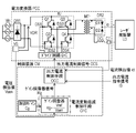
- FIG. 1 illustrates a configuration of a laser driving power source of a laser oscillator according to an aspect of the present disclosure.
- This drive power supply is a laser drive power supply that includes a power converter PCC and a control device CM and performs power conversion to obtain a current and voltage suitable for the laser oscillator LD.
- the power converter PCC includes a primary rectifier circuit DR1, an inverter unit IU, a power conversion transformer MTr, and a secondary rectifier circuit DR2.
- the primary rectifier circuit DR1 rectifies the input voltage Vin of AC power and converts it into a DC voltage.
- the inverter unit IU converts a DC voltage into an AC voltage.
- the power conversion transformer MTr converts the AC voltage into power to generate a secondary current.
- the secondary rectifier circuit DR2 rectifies the secondary current and converts it into an output current supplied to the laser oscillator LD.
- the power converter PCC further includes a drive circuit DrC and an output current detection circuit CT.
- the drive circuit DrC outputs a drive signal DS that drives a semiconductor switch constituting the inverter unit IU.
- the output current detection circuit CT detects the output current io and outputs an output current detection value ict.
- the control device CM includes a current fluctuation reduction control unit CFC, an output current control unit OCC, and a control gain Cg.
- the current fluctuation reduction control means CFC outputs an adjuster signal IK for reducing fluctuations in responsiveness of the output current io due to fluctuations in the input voltage.
- the output current control means OCC controls the inverter unit IU so that the output current io becomes equal to the output current command signal IS which is a control target.
- the control gain Cg is used to calculate an operation amount that is controlled with respect to a deviation between the output current detection value ict indicating the output current io and the output current command signal IS indicating the control target.
- FIG. 2 shows a configuration of a laser driving power source of the laser oscillator according to the first embodiment of the present disclosure.
- the primary rectifier circuit DR1 rectifies the input voltage Vin, which is a three-phase AC, and converts it into a rectified voltage VDR, which is a DC voltage.
- the inverter unit IU includes a first circuit unit having a first switching element Q1 and a second switching element Q2, and a second circuit unit having a third switching element Q3 and a fourth switching element Q4. Is provided.
- the first circuit unit is connected in parallel to the second circuit unit.
- the first switching element Q1 is connected in series to the second switching element Q2.
- the third switching element Q3 is connected in series to the fourth switching element Q4.
- the inverter unit IU converts the rectified voltage VDR into an AC voltage by controlling each switching element.
- the switching element may be a semiconductor switch such as an IGBT (Insulated Gate Bipolar Transistor) or a MOSFET (Metal Oxide Semiconductor Field Effect Transistor).
- IGBT Insulated Gate Bipolar Transistor
- MOSFET Metal Oxide Semiconductor Field Effect Transistor
- the power conversion transformer MTr includes a primary side coil and a secondary side coil.
- the primary coil is connected between the emitter of the first switching element Q1 and the collector of the fourth switching element Q4.
- the power conversion transformer MTr converts the AC voltage input to the primary side coil, and outputs a voltage and current suitable for the laser oscillator LD from the secondary side coil.
- the secondary coil of the power conversion transformer MTr has an intermediate tap.
- the secondary rectifier circuit DR2 has a configuration in which the cathode of the first diode D1 and the cathode of the second diode D2 are connected.
- the secondary side alternating current of the power conversion transformer MTr is converted into an output current io which is a direct current.
- the anode of the first diode D1 is connected to one end of the secondary side coil of the power conversion transformer MTr, and the anode of the second diode D2 is connected to the other end of the secondary side coil.
- the cathodes of the first diode D1 and the second diode D2 are connected to the + terminal of the laser oscillator LD.
- the intermediate tap of the power conversion transformer MTr and one end of the DC reactor DCL are connected, and the other end of the DC reactor DCL and the minus terminal of the laser oscillator LD are connected.
- the direct current reactor DCL smoothes the output current io.
- the power converter PCC supplies an output current io suitable for the laser oscillator LD to the laser oscillator LD.
- the output current detection circuit CT is installed on the wiring connected to the laser oscillator LD, and outputs the output current detection value ict.
- the control device CM includes an output current control means OCC, a control gain Cg, and a current command regulator Ks that is a current fluctuation reduction control means CFC that reduces fluctuations in the response of the output current io.
- the output current command signal IS is a set value signal related to the output current io that is externally input or internally generated and adjusted by the operator, and is a signal that indicates a control target of the output current io.
- the output current command signal IS is input to the current command adjuster Ks.
- the current command adjuster Ks includes a first-order lag element (for example, a first-order low-pass filter) that generates a first-order lag.
- a filter design method for the current command regulator Ks will be described with reference to FIGS. 2, 3, and 4.
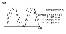
- FIG. 3 shows fluctuations in the response of the output current io when the output current command signal IS is input.
- the response of the output current io is fast when the input voltage Vin is high as indicated by a one-dot chain line, and the input voltage Vin is low as indicated by a two-dot chain line. Then, the response of the output current becomes slow. Therefore, the waveform of the output current io changes due to the fluctuation of the input voltage Vin.
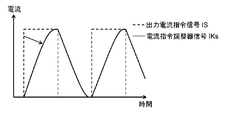
- FIG. 4 shows the generation of the current command regulator signal IKs when the output current command signal IS is input.
- the current command regulator Ks generates the current command regulator signal IKs represented by the solid line with a delay as described above with respect to the output current command signal IS represented by the broken line.
- the response of the output current io is the slowest when the minimum voltage Vm is within the range of the input voltage Vin guaranteed by the laser drive power supply. Therefore, the responsiveness of the output current io is measured when the minimum voltage Vm is input as the input voltage Vin and the pulse signal is input as the output current command signal IS to operate the laser driving power source.
- the filter characteristic of the first-order lag filter in the current command regulator Ks is designed so that the change of the pulse signal is equal to or less than the measured response.
- the output current control means OCC generates the output current control signal OCS using the output current detection value ict, the current command adjuster signal IKs, and the control gain Cg.
- the control gain Cg is used to calculate an operation amount that is controlled with respect to the deviation between the output current detection value ict and the current command regulator signal IKs.
- the output current control signal OCS is a signal for controlling the inverter unit IU so that the output current io becomes equal to the current command regulator signal IKs.
- the drive circuit DrC generates a first drive signal DS1, a second drive signal DS2, a third drive signal DS3, and a fourth drive signal DS4 based on the output current control signal OCS.
- the first drive signal DS1 drives the first switching element Q1.
- the second drive signal DS2 drives the second switching element Q2.
- the third drive signal DS3 drives the third switching element Q3.
- the fourth drive signal DS4 drives the fourth switching element Q4. Thereby, the output current io is controlled.
- FIG. 5 shows a configuration of a laser driving power source of the laser oscillator according to the second embodiment of the present disclosure.
- the current command regulator Ks is employed as current fluctuation reduction control means CFC that reduces the responsiveness fluctuation of the output current io of the control device CM.
- the gain adjuster Kg is employed as the current fluctuation reduction control means CFC.
- the power converter PCC includes a voltage detection circuit VS that detects a rectified voltage VDR that is a voltage after the input voltage Vin is rectified by the primary rectifier circuit DR1. Since the main circuit operation is the same as in the first embodiment, only the control method of the control device CM different from the first embodiment will be described.
- the voltage detection circuit VS is connected in parallel to the primary rectifier circuit DR1 in order to detect the rectified voltage VDR between the output terminals of the primary rectifier circuit DR1.
- the voltage detection value Vsen and the control gain Cg obtained from the voltage detection circuit VS are input to the gain adjuster Kg.
- the gain adjuster Kg multiplies the control gain Cg by a coefficient that is inversely proportional to the detected voltage value Vsen.
- the coefficient of the gain adjuster Kg is a value obtained by dividing the reference input voltage Vref by the voltage detection value Vsen.
- the gain adjuster Kg multiplies the control gain Cg by the coefficient of the gain adjuster Kg to generate a gain adjuster signal IKg.
- FIG. 6 shows the relationship between the voltage detection value Vsen and the gain adjuster signal IKg.
- the reference input voltage Vref is a value equivalent to the detected voltage value Vsen in the case of the median value of the fluctuation of the input voltage Vin. For example, when the guaranteed range of the input voltage Vin is 160V to 240V, the reference input voltage Vref matches the voltage detection value Vsen when the median is 200V.
- the output current control means OCC generates the output current control signal OCS using the gain adjuster signal IKg, the output current detection value ict, and the output current command signal IS.
- the output current control signal OCS is a signal for controlling the inverter unit IU so that the output current io becomes equal to the output current command signal IS.
- the output current control signal OCS is a signal for controlling the continuity Duty, which is the ratio at which the inverter unit IU supplies voltage or current to the power conversion transformer MTr.
- the drive circuit DrC generates a first drive signal DS1, a second drive signal DS2, a third drive signal DS3, and a fourth drive signal DS4 based on the output current control signal OCS.
- the first drive signal DS1 drives the first switching element Q1.
- the second drive signal DS2 drives the second switching element Q2.
- the third drive signal DS3 drives the third switching element Q3.
- the fourth drive signal DS4 drives the fourth switching element Q4. Thereby, the output current io is controlled.
- the coefficient of the gain adjuster Kg becomes smaller than 1. Then, the gain adjuster signal IKg becomes smaller than the control gain Cg, and the continuity Duty of the inverter unit IU is adjusted to be low. This slows down the response of the output current io.
- the coefficient of the gain adjuster Kg becomes larger than 1.
- the gain adjuster signal IKg becomes larger than the control gain Cg, and the continuity Duty of the inverter unit IU is adjusted to be high. This speeds up the response of the output current io.
- the responsiveness of the output current io can be controlled according to the fluctuation of the input voltage Vin. Therefore, it is possible to supply the output current io with reduced responsiveness variation due to variation in the input voltage Vin.
- the laser driving power source is a laser driving power source for supplying a current for outputting laser light to the laser oscillator LD to drive the laser oscillator LD.
- the laser driving power source is composed of a power converter PCC and a control device CM.
- the power converter PCC includes a primary rectifier circuit DR1, an inverter unit IU, a power conversion transformer MTr, and a secondary rectifier circuit DR2.
- the primary rectifier circuit DR1 rectifies the input voltage Vin of AC power and converts it into a DC voltage.
- the inverter unit IU converts a DC voltage into an AC voltage.
- the power conversion transformer MTr converts the AC voltage into power to generate a secondary current.
- the secondary rectifier circuit DR2 rectifies the secondary current and converts it into an output current supplied to the laser oscillator LD.
- the power converter PCC further includes a drive circuit DrC and an output current detection circuit CT.
- the drive circuit DrC outputs a drive signal that drives a semiconductor switch that constitutes the inverter unit IU.
- the output current detection circuit CT detects the output current io and outputs an output current detection value ict.
- the controller CM detects the output current detection value ict, the output current command signal IS, or A current for generating a regulator signal IK by adjusting at least one of the control gains Cg so as to reduce fluctuations in the response of the output current io due to fluctuations in the input voltage Vin, and outputting a regulator signal It has fluctuation reduction control means CFC.
- control device CM outputs all the signals that have not been adjusted by the current fluctuation reduction control means CFC among the output current detection value ict, the output current command signal IS, and the control gain Cg, and the regulator signal IK.
- output current control means OCC for outputting the output current control signal OCS.
- the current fluctuation reduction control means CFC may adjust the output current command signal IS.
- the current fluctuation reduction control means CFC may include a current command adjuster Ks that generates the current command adjuster signal IKs by adjusting the output current command signal IS.
- the current command regulator Ks generates a primary delay so that the change in the output current command signal IS is delayed in response to the response of the slowest output current io in the voltage range guaranteed with respect to the input voltage Vin. Has a delay element.
- An output current command signal IS is input to the current command adjuster Ks.
- the laser driving power source controls the output current io with a slight delay or little delay with respect to the current command regulator signal IKs regardless of the fluctuation of the input voltage Vin by delaying the change of the output current command signal IS. .
- control of the output current io with a slight delay with respect to the output current command signal IS is a slight delay that allows for variations in the processing accuracy of the laser processing machine.
- the current fluctuation reduction control means CFC may adjust the control gain Cg.
- the power converter PCC includes a voltage detection circuit VS that detects the input voltage Vin or the rectified voltage VDR.
- the current fluctuation reduction control means CFC includes a gain adjuster Kg that adjusts the control gain Cg according to the voltage detection value Vsen by multiplying the control gain Cg by a coefficient inversely proportional to the voltage detection value Vsen.
- the laser drive power supply controls the continuity Duty of the inverter unit IU according to the voltage detection value Vsen and controls the response of the output current io, thereby changing the response of the output current io. It is to reduce.
- the laser driving power source has a function of the control device CM including the current fluctuation reduction control unit CFC, and the output current io due to the fluctuation of the input voltage Vin. Reduce fluctuations in responsiveness.
- the control device CM has a parameter for adjusting the output current command signal IS or the control gain Cg related to control.
- the current fluctuation reduction control means CFC functions as an adjuster for adjusting any of the output current command signal IS, the output current detection value ict, or the control gain Cg.
- Such a laser drive power supply can eliminate fluctuations in output current due to fluctuations in input voltage, and can reduce fluctuations in the output of laser light. Thereby, the improvement of processing accuracy can be provided. Furthermore, the above laser drive power supply does not require an additional power converter or an additional element. Therefore, cost reduction and high efficiency can be achieved.
- control device CM of the second embodiment approaches the responsiveness of the output current io at the reference input voltage Vref. Therefore, compared with the first embodiment, it is possible to increase the response of the output current io and reduce the response variation. However, when the adjusted conductivity Duty exceeds the upper limit of the conductivity Duty, the effect of reducing responsiveness variation is reduced. In the first embodiment, the influence of other parameters is small, and a certain reduction effect can be obtained.
- the output current command signal IS is adjusted in order to reduce fluctuations in output current response due to fluctuations in input voltage.
- the control gain Cg is adjusted instead.
- the present disclosure is not limited to this, and the output current detection value ict may be adjusted. Adjustment of the output current detection value ict can also reduce fluctuations in output current response due to fluctuations in the input voltage.
- the output current command signal IS and in the second embodiment, the control gain Cg.
- the present disclosure is not limited to this, and two or three signals may be adjusted.
- the two signals of the output current command signal IS and the control gain Cg may be adjusted.
- three signals of the output current detection value ict, the output current command signal IS, and the control gain Cg may be adjusted.
- the present disclosure is industrially useful as a control method capable of reducing variations in machining accuracy of a laser processing machine equipped with a laser oscillator by reducing fluctuations in the output current of the laser driving power source of the laser oscillator due to fluctuations in the input voltage. .
Landscapes
- Engineering & Computer Science (AREA)
- Power Engineering (AREA)
- Physics & Mathematics (AREA)
- Electromagnetism (AREA)
- Plasma & Fusion (AREA)
- Optics & Photonics (AREA)
- Mechanical Engineering (AREA)
- Dc-Dc Converters (AREA)
- Semiconductor Lasers (AREA)
- Inverter Devices (AREA)
Abstract
Description
本実施の形態について、図1から図4を用いて説明をする。図1は本開示の一態様によるレーザ発振器のレーザ用の駆動電源の構成を示している。この駆動電源は、電力変換器PCCと制御装置CMとを備え、レーザ発振器LDに適した電流と電圧を得るための電力変換を行うレーザ駆動電源である。電力変換器PCCは、一次整流回路DR1と、インバータユニットIUと、電力変換トランスMTrと、二次整流回路DR2と、を備える。一次整流回路DR1は、交流電力の入力電圧Vinを整流し、直流電圧に変換する。インバータユニットIUは、直流電圧を交流電圧に変換する。電力変換トランスMTrは、交流電圧を電力変換して二次電流を生成する。二次整流回路DR2は、二次電流を整流しレーザ発振器LDに供給される出力電流に変換する。
次に実施の形態2について図5から図6を用いて説明する。図5は本開示の実施の形態2によるレーザ発振器のレーザ駆動電源の構成を示している。実施の形態1では、電流指令調整器Ksが、制御装置CMが有する出力電流ioの応答性変動を低減する電流変動低減制御手段CFCとして採用されている。これに対して、実施の形態2では、ゲイン調整器Kgが、電流変動低減制御手段CFCとして採用されている。さらに、実施の形態2では、電力変換器PCCは、一次整流回路DR1により入力電圧Vinが整流された後の電圧である整流電圧VDRを検出する電圧検出回路VSを備える。主な回路動作は実施の形態1と同様なため、実施の形態1と異なる制御装置CMの、制御方法についてのみ説明する。
PCC 電力変換器
DR1 一次整流回路
IU インバータユニット
VDR 整流電圧
Q1 第1のスイッチング素子
Q2 第2のスイッチング素子
Q3 第3のスイッチング素子
Q4 第4のスイッチング素子
MTr 電力変換トランス
DR2 二次整流回路
D1 第1のダイオード
D2 第2のダイオード
DCL 直流リアクトル
io 出力電流
LD レーザ発振器
CT 出力電流検出回路
ict 出力電流検出値
CM 制御装置
CFC 電流変動低減制御手段
IK 調整器信号
OCC 出力電流制御手段
Cg 制御ゲイン
Ks 電流指令調整器
IS 出力電流指令信号
IKs 電流指令調整器信号
Vm 最低電圧
OCS 出力電流制御信号
DrC ドライブ回路
DS1 第1のドライブ信号
DS2 第2のドライブ信号
DS3 第3のドライブ信号
DS4 第4のドライブ信号
VS 電圧検出回路
Vsen 電圧検出値
Kg ゲイン調整器
Vref 基準入力電圧
IKg ゲイン調整器信号
Duty 導通率
Claims (3)
- レーザ光を出力するための電流をレーザ発振器に対して供給し、前記レーザ発振器を駆動するためのレーザ駆動電源であって、
交流電力の入力電圧を整流し直流電圧に変換する一次整流回路と、
前記直流電圧を交流電圧に変換するインバータユニットと、
前記交流電圧を電力変換して二次電流を生成する電力変換トランスと、
前記二次電流を整流し前記レーザ発振器に供給される出力電流に変換する二次整流回路と、
前記インバータユニットを構成する半導体スイッチを駆動するドライブ信号を出力するドライブ回路と、
前記出力電流を検出し電流検出値を出力する出力電流検出手段と、
を有する電力変換器と、
前記出力電流の応答性に対して、前記出力電流の制御目標である出力電流指令信号の変化が速い場合、前記電流検出値、前記出力電流指令信号、および、前記電流検出値と前記出力電流指令信号の偏差に対して制御する操作量の演算に用いる制御ゲインの、少なくともいずれか一つの信号を、前記入力電圧の変動による前記出力電流の応答性の変動を低減するように調整して調整器信号を生成し、前記調整器信号を出力する電流変動低減制御手段と、
前記電流検出値、前記出力電流指令信号、および、前記制御ゲインの内で、前記電流変動低減制御手段で調整されなかった信号と前記調整器信号とを用いて、前記出力電流を制御するために前記ドライブ回路に入力する出力電流制御信号を出力する出力電流制御手段と、
を有する制御装置と、
を有するレーザ駆動電源。 - 前記少なくともいずれか一つの信号は、前記出力電流指令信号であり、
前記電力変換器は、前記入力電圧に対して保障する電圧範囲を有し、
前記制御装置における前記電流変動低減制御手段は、前記保障された電圧範囲において、最も遅い前記出力電流の応答性に対応して、前記出力電流指令信号の変化が遅くなるように前記出力電流指令信号を調整する電流指令調整器を有し、
前記電流指令調整器は前記出力電流指令信号に一次遅れを発生させて前記調整器信号を生成する一次遅れ要素を有し、
前記出力電流指令信号の変化を遅らせることで、前記入力電圧の変動に関係なく、前記調整器信号に対して遅れなく、または、わずかな遅れで前記出力電流を制御可能とする、
請求項1記載のレーザ駆動電源。 - 前記少なくともいずれか一つの信号は、前記制御ゲインであり、
前記電力変換器は、前記入力電圧、または前記直流電圧を検出し電圧検出値を出力する入力電圧検出手段を有し、
前記制御装置の前記電流変動低減制御手段は、前記電圧検出値に反比例した係数を前記制御ゲインに乗算することで、前記制御ゲインを前記電圧検出値に応じて調整するゲイン調整器を有し、
前記電圧検出値に応じて前記インバータユニットの導通率を制御し、前記出力電流の応答性を制御することで、前記出力電流の応答性変動を低減する請求項1記載のレーザ駆動電源。
Priority Applications (4)
| Application Number | Priority Date | Filing Date | Title |
|---|---|---|---|
| CN201880022307.8A CN110463005B (zh) | 2017-04-05 | 2018-03-05 | 激光驱动电源 |
| JP2019511103A JP7108825B2 (ja) | 2017-04-05 | 2018-03-05 | レーザ駆動電源 |
| EP18781415.7A EP3609064A4 (en) | 2017-04-05 | 2018-03-05 | LASER DRIVING POWER SOURCE |
| US16/497,454 US10938306B2 (en) | 2017-04-05 | 2018-03-05 | Laser driving power source |
Applications Claiming Priority (2)
| Application Number | Priority Date | Filing Date | Title |
|---|---|---|---|
| JP2017074961 | 2017-04-05 | ||
| JP2017-074961 | 2017-04-05 |
Publications (1)
| Publication Number | Publication Date |
|---|---|
| WO2018186082A1 true WO2018186082A1 (ja) | 2018-10-11 |
Family
ID=63712760
Family Applications (1)
| Application Number | Title | Priority Date | Filing Date |
|---|---|---|---|
| PCT/JP2018/008227 Ceased WO2018186082A1 (ja) | 2017-04-05 | 2018-03-05 | レーザ駆動電源 |
Country Status (5)
| Country | Link |
|---|---|
| US (1) | US10938306B2 (ja) |
| EP (1) | EP3609064A4 (ja) |
| JP (1) | JP7108825B2 (ja) |
| CN (1) | CN110463005B (ja) |
| WO (1) | WO2018186082A1 (ja) |
Cited By (3)
| Publication number | Priority date | Publication date | Assignee | Title |
|---|---|---|---|---|
| WO2022176948A1 (ja) * | 2021-02-19 | 2022-08-25 | パナソニックIpマネジメント株式会社 | レーザ発振器及びそれを備えたダイレクトダイオードレーザ加工装置 |
| EP4107825A4 (en) * | 2020-03-31 | 2024-03-27 | IPG Photonics Corporation | HIGH PERFORMANCE LASER ELECTRONICS |
| CN118889173A (zh) * | 2024-09-27 | 2024-11-01 | 深圳市联明电源股份有限公司 | 一种基于自动调节的激光电源控制方法及系统 |
Families Citing this family (4)
| Publication number | Priority date | Publication date | Assignee | Title |
|---|---|---|---|---|
| CN108418569B (zh) * | 2018-05-25 | 2018-11-09 | 敏业信息科技(上海)有限公司 | 差模电磁噪声注入网络及有源电磁干扰滤波器 |
| CN111431027B (zh) * | 2020-03-30 | 2021-07-16 | 武汉光谷信息光电子创新中心有限公司 | 一种关电控制方法、电路、装置和存储介质 |
| US20230311230A1 (en) * | 2022-04-04 | 2023-10-05 | Esab Ab | Cancellation of the effects of primary voltage variations |
| CN115987083B (zh) * | 2023-03-14 | 2023-06-06 | 合肥乘翎微电子有限公司 | 降低电磁辐射的控制电路及其控制方法、及隔离电源系统 |
Citations (4)
| Publication number | Priority date | Publication date | Assignee | Title |
|---|---|---|---|---|
| JPH0241778A (ja) | 1988-08-01 | 1990-02-09 | Hitachi Seiko Ltd | インバータ溶接機 |
| JPH02140984A (ja) * | 1988-11-22 | 1990-05-30 | Nec Corp | エンハンスドパルス電流発生用レーザ電源 |
| JP2009012028A (ja) * | 2007-07-03 | 2009-01-22 | Daihen Corp | アーク溶接用電源装置 |
| WO2016175137A1 (ja) * | 2015-04-28 | 2016-11-03 | 三菱電機株式会社 | レーザ発振器 |
Family Cites Families (20)
| Publication number | Priority date | Publication date | Assignee | Title |
|---|---|---|---|---|
| US4070699A (en) * | 1975-11-10 | 1978-01-24 | Datascope Corporation | Charging circuits using controlled magnetic fields |
| US4355351A (en) * | 1979-05-30 | 1982-10-19 | Schwarz Francisc C | High repetition rate power pulse generator |
| JP3235331B2 (ja) | 1994-03-11 | 2001-12-04 | 富士電機株式会社 | 電流制御回路 |
| US6384579B2 (en) * | 2000-06-27 | 2002-05-07 | Origin Electric Company, Limited | Capacitor charging method and charging apparatus |
| JP4772957B2 (ja) | 2000-12-26 | 2011-09-14 | 株式会社ダイヘン | レーザ照射交流アーク溶接方法 |
| JP4135417B2 (ja) | 2002-07-09 | 2008-08-20 | 三菱電機株式会社 | レーザ電源装置及びレーザ装置 |
| US7911816B2 (en) * | 2006-09-13 | 2011-03-22 | Hypertherm, Inc. | Linear, inductance based control of regulated electrical properties in a switch mode power supply of a thermal processing system |
| JP5550648B2 (ja) * | 2009-07-27 | 2014-07-16 | 三菱電機株式会社 | 高周波電源装置 |
| WO2011048796A1 (ja) * | 2009-10-19 | 2011-04-28 | パナソニック株式会社 | Dc-dcコンバータ |
| JP5924281B2 (ja) * | 2013-02-01 | 2016-05-25 | 三菱電機株式会社 | 電力変換装置及び系統連系システム |
| KR101582471B1 (ko) * | 2014-06-11 | 2016-01-07 | 한국에너지기술연구원 | 효율맵을 이용하는 컨버터시스템 및 그 제어방법 |
| JP6379730B2 (ja) | 2014-06-25 | 2018-08-29 | 株式会社Soken | 電力変換装置 |
| WO2016002001A1 (ja) | 2014-07-01 | 2016-01-07 | ギガフォトン株式会社 | レーザ装置、euv光生成システム及びレーザ装置の制御方法 |
| CN107534270B (zh) * | 2015-04-15 | 2020-01-21 | 三菱电机株式会社 | 激光二极管驱动用电源装置 |
| JP6671879B2 (ja) * | 2015-07-21 | 2020-03-25 | キヤノン株式会社 | 高圧電源装置及び画像形成装置 |
| JP2017046403A (ja) | 2015-08-25 | 2017-03-02 | 株式会社ダイヘン | インバータ制御回路、インバータ制御方法、および、電源装置 |
| CN105119494B (zh) * | 2015-09-09 | 2018-04-03 | 广东康氏实业有限公司 | 一种激光电脑绣花机的激光发生器高压直流稳压电源电路 |
| CN108370130B (zh) * | 2015-12-01 | 2019-11-01 | 三菱电机株式会社 | 电流控制装置及电流控制方法 |
| JP6316792B2 (ja) * | 2015-12-04 | 2018-04-25 | ファナック株式会社 | 複数の発光素子を制御するレーザ電源装置 |
| JP6754669B2 (ja) * | 2016-10-31 | 2020-09-16 | 株式会社ダイヘン | 給電側装置および給電システム |
-
2018
- 2018-03-05 US US16/497,454 patent/US10938306B2/en active Active
- 2018-03-05 JP JP2019511103A patent/JP7108825B2/ja active Active
- 2018-03-05 EP EP18781415.7A patent/EP3609064A4/en not_active Withdrawn
- 2018-03-05 WO PCT/JP2018/008227 patent/WO2018186082A1/ja not_active Ceased
- 2018-03-05 CN CN201880022307.8A patent/CN110463005B/zh active Active
Patent Citations (4)
| Publication number | Priority date | Publication date | Assignee | Title |
|---|---|---|---|---|
| JPH0241778A (ja) | 1988-08-01 | 1990-02-09 | Hitachi Seiko Ltd | インバータ溶接機 |
| JPH02140984A (ja) * | 1988-11-22 | 1990-05-30 | Nec Corp | エンハンスドパルス電流発生用レーザ電源 |
| JP2009012028A (ja) * | 2007-07-03 | 2009-01-22 | Daihen Corp | アーク溶接用電源装置 |
| WO2016175137A1 (ja) * | 2015-04-28 | 2016-11-03 | 三菱電機株式会社 | レーザ発振器 |
Non-Patent Citations (1)
| Title |
|---|
| See also references of EP3609064A4 |
Cited By (5)
| Publication number | Priority date | Publication date | Assignee | Title |
|---|---|---|---|---|
| EP4107825A4 (en) * | 2020-03-31 | 2024-03-27 | IPG Photonics Corporation | HIGH PERFORMANCE LASER ELECTRONICS |
| US12051888B2 (en) | 2020-03-31 | 2024-07-30 | Ipg Photonics Corporation | High powered laser electronics |
| US12362678B1 (en) | 2020-03-31 | 2025-07-15 | Ipg Photonics Corporation | High powered laser electronics |
| WO2022176948A1 (ja) * | 2021-02-19 | 2022-08-25 | パナソニックIpマネジメント株式会社 | レーザ発振器及びそれを備えたダイレクトダイオードレーザ加工装置 |
| CN118889173A (zh) * | 2024-09-27 | 2024-11-01 | 深圳市联明电源股份有限公司 | 一种基于自动调节的激光电源控制方法及系统 |
Also Published As
| Publication number | Publication date |
|---|---|
| EP3609064A4 (en) | 2020-04-01 |
| EP3609064A1 (en) | 2020-02-12 |
| CN110463005A (zh) | 2019-11-15 |
| JPWO2018186082A1 (ja) | 2020-02-13 |
| US10938306B2 (en) | 2021-03-02 |
| JP7108825B2 (ja) | 2022-07-29 |
| CN110463005B (zh) | 2021-06-08 |
| US20200287460A1 (en) | 2020-09-10 |
Similar Documents
| Publication | Publication Date | Title |
|---|---|---|
| JP7108825B2 (ja) | レーザ駆動電源 | |
| CN113639564B (zh) | 用于一电弧炉的供电装置及方法 | |
| CN102138277B (zh) | 可自动优化效率的开关模式电源 | |
| JP5170315B2 (ja) | アーク溶接方法およびアーク溶接装置 | |
| US10104732B2 (en) | LED drive method and LED drive device | |
| JP2012501156A5 (ja) | ||
| JP6145698B2 (ja) | アーク溶接制御方法およびアーク溶接装置 | |
| TWI446138B (zh) | 風力發電之激磁式同步發電機系統的控制方法 | |
| JP6161998B2 (ja) | 電源装置及びアーク加工用電源装置 | |
| CN112840549A (zh) | 逆变器装置的测试装置 | |
| JP2012200781A (ja) | 静電蓄勢式溶接電源の充電制御方法および静電蓄勢式溶接電源 | |
| US10239144B2 (en) | Welding device | |
| JP2015186407A (ja) | 電力変換装置 | |
| JPWO2007108427A1 (ja) | 電圧調整装置 | |
| CN107947564A (zh) | 电压转换装置及机器 | |
| US10989474B2 (en) | Integrated flicker control for arc furnace | |
| CN116635181B (zh) | 用于限制焊接设备的焊接功率的方法 | |
| JP2017055535A (ja) | 太陽光発電用電力変換装置および太陽光発電システム | |
| CN107947582A (zh) | 电压转换装置及机器 | |
| JP2024019836A (ja) | レーザ駆動電源 | |
| JP6510972B2 (ja) | インバータ制御回路、および、電源装置 | |
| US20230311230A1 (en) | Cancellation of the effects of primary voltage variations | |
| JP2005285379A (ja) | 昇圧チョッパの制御システム | |
| EP4606507A1 (en) | Submerged arc welding control method | |
| JP2020202064A (ja) | 電源システム、電源システムの制御装置、および電源システムの制御方法 |
Legal Events
| Date | Code | Title | Description |
|---|---|---|---|
| 121 | Ep: the epo has been informed by wipo that ep was designated in this application |
Ref document number: 18781415 Country of ref document: EP Kind code of ref document: A1 |
|
| ENP | Entry into the national phase |
Ref document number: 2019511103 Country of ref document: JP Kind code of ref document: A |
|
| NENP | Non-entry into the national phase |
Ref country code: DE |
|
| ENP | Entry into the national phase |
Ref document number: 2018781415 Country of ref document: EP Effective date: 20191105 |
|
| WWW | Wipo information: withdrawn in national office |
Ref document number: 2018781415 Country of ref document: EP |