WO2018192220A1 - 一种超结构光栅和可调谐激光器 - Google Patents
一种超结构光栅和可调谐激光器 Download PDFInfo
- Publication number
- WO2018192220A1 WO2018192220A1 PCT/CN2017/112142 CN2017112142W WO2018192220A1 WO 2018192220 A1 WO2018192220 A1 WO 2018192220A1 CN 2017112142 W CN2017112142 W CN 2017112142W WO 2018192220 A1 WO2018192220 A1 WO 2018192220A1
- Authority
- WO
- WIPO (PCT)
- Prior art keywords
- mirror
- layer
- grating
- region
- tunable laser
- Prior art date
- Legal status (The legal status is an assumption and is not a legal conclusion. Google has not performed a legal analysis and makes no representation as to the accuracy of the status listed.)
- Ceased
Links
Images


Classifications
-
- G—PHYSICS
- G02—OPTICS
- G02B—OPTICAL ELEMENTS, SYSTEMS OR APPARATUS
- G02B5/00—Optical elements other than lenses
- G02B5/18—Diffraction gratings
- G02B5/1866—Transmission gratings characterised by their structure, e.g. step profile, contours of substrate or grooves, pitch variations, materials
- G02B5/1871—Transmissive phase gratings
-
- G—PHYSICS
- G02—OPTICS
- G02B—OPTICAL ELEMENTS, SYSTEMS OR APPARATUS
- G02B5/00—Optical elements other than lenses
- G02B5/18—Diffraction gratings
-
- H—ELECTRICITY
- H01—ELECTRIC ELEMENTS
- H01S—DEVICES USING THE PROCESS OF LIGHT AMPLIFICATION BY STIMULATED EMISSION OF RADIATION [LASER] TO AMPLIFY OR GENERATE LIGHT; DEVICES USING STIMULATED EMISSION OF ELECTROMAGNETIC RADIATION IN WAVE RANGES OTHER THAN OPTICAL
- H01S5/00—Semiconductor lasers
- H01S5/50—Amplifier structures not provided for in groups H01S5/02 - H01S5/30
- H01S5/5063—Amplifier structures not provided for in groups H01S5/02 - H01S5/30 operating above threshold
- H01S5/5072—Gain clamping, i.e. stabilisation by saturation using a further mode or frequency
-
- H—ELECTRICITY
- H01—ELECTRIC ELEMENTS
- H01S—DEVICES USING THE PROCESS OF LIGHT AMPLIFICATION BY STIMULATED EMISSION OF RADIATION [LASER] TO AMPLIFY OR GENERATE LIGHT; DEVICES USING STIMULATED EMISSION OF ELECTROMAGNETIC RADIATION IN WAVE RANGES OTHER THAN OPTICAL
- H01S5/00—Semiconductor lasers
- H01S5/06—Arrangements for controlling the laser output parameters, e.g. by operating on the active medium
-
- H—ELECTRICITY
- H01—ELECTRIC ELEMENTS
- H01S—DEVICES USING THE PROCESS OF LIGHT AMPLIFICATION BY STIMULATED EMISSION OF RADIATION [LASER] TO AMPLIFY OR GENERATE LIGHT; DEVICES USING STIMULATED EMISSION OF ELECTROMAGNETIC RADIATION IN WAVE RANGES OTHER THAN OPTICAL
- H01S5/00—Semiconductor lasers
- H01S5/06—Arrangements for controlling the laser output parameters, e.g. by operating on the active medium
- H01S5/0607—Arrangements for controlling the laser output parameters, e.g. by operating on the active medium by varying physical parameters other than the potential of the electrodes, e.g. by an electric or magnetic field, mechanical deformation, pressure, light, temperature
-
- H—ELECTRICITY
- H01—ELECTRIC ELEMENTS
- H01S—DEVICES USING THE PROCESS OF LIGHT AMPLIFICATION BY STIMULATED EMISSION OF RADIATION [LASER] TO AMPLIFY OR GENERATE LIGHT; DEVICES USING STIMULATED EMISSION OF ELECTROMAGNETIC RADIATION IN WAVE RANGES OTHER THAN OPTICAL
- H01S5/00—Semiconductor lasers
- H01S5/10—Construction or shape of the optical resonator, e.g. extended or external cavity, coupled cavities, bent-guide, varying width, thickness or composition of the active region
- H01S5/12—Construction or shape of the optical resonator, e.g. extended or external cavity, coupled cavities, bent-guide, varying width, thickness or composition of the active region the resonator having a periodic structure, e.g. in distributed feedback [DFB] lasers
- H01S5/124—Construction or shape of the optical resonator, e.g. extended or external cavity, coupled cavities, bent-guide, varying width, thickness or composition of the active region the resonator having a periodic structure, e.g. in distributed feedback [DFB] lasers incorporating phase shifts
-
- H—ELECTRICITY
- H04—ELECTRIC COMMUNICATION TECHNIQUE
- H04B—TRANSMISSION
- H04B10/00—Transmission systems employing electromagnetic waves other than radio-waves, e.g. infrared, visible or ultraviolet light, or employing corpuscular radiation, e.g. quantum communication
- H04B10/25—Arrangements specific to fibre transmission
- H04B10/2589—Bidirectional transmission
- H04B10/25891—Transmission components
-
- H—ELECTRICITY
- H04—ELECTRIC COMMUNICATION TECHNIQUE
- H04B—TRANSMISSION
- H04B10/00—Transmission systems employing electromagnetic waves other than radio-waves, e.g. infrared, visible or ultraviolet light, or employing corpuscular radiation, e.g. quantum communication
- H04B10/50—Transmitters
- H04B10/501—Structural aspects
- H04B10/503—Laser transmitters
-
- G—PHYSICS
- G02—OPTICS
- G02B—OPTICAL ELEMENTS, SYSTEMS OR APPARATUS
- G02B27/00—Optical systems or apparatus not provided for by any of the groups G02B1/00 - G02B26/00, G02B30/00
- G02B27/0012—Optical design, e.g. procedures, algorithms, optimisation routines
-
- G—PHYSICS
- G02—OPTICS
- G02B—OPTICAL ELEMENTS, SYSTEMS OR APPARATUS
- G02B5/00—Optical elements other than lenses
- G02B5/18—Diffraction gratings
- G02B5/1814—Diffraction gratings structurally combined with one or more further optical elements, e.g. lenses, mirrors, prisms or other diffraction gratings
Definitions
- the present application relates to the field of optical fiber communications, and in particular to a superstructure grating and a tunable laser.
- a tunable laser refers to a laser that can adjust the wavelength of an output optical signal within a certain range, and is mainly used in a large-capacity wavelength division multiplexing transmission system.
- coherent modulation technology is used and becomes the mainstream solution for long-distance optical transmission of 100G and above.
- Coherent modulation techniques have stringent requirements on the laser's excitation raywidth and other performance requirements.
- Various new requirements also place higher demands on the size, cost, reliability and performance of tunable lasers.
- the monolithic integrated tunable laser has the advantages of small size and high integration, and thus has become the mainstream technology in the field of optical communication.
- a monolithically integrated tunable laser can be fabricated substantially through the docking of the gain region with an inactive region on an Indium Phosphide (InP) substrate.
- the gain region is generally a multiple quantum well (MQW), while the passive region mainly includes a mirror and a phase segment. Wavelength tuning is achieved by adjusting the refractive index of the mirror or phase segment.
- the reflection spectrum of the mirror is selective to the wavelength, and the commonly used mirror includes a distributed Bragg Reflection (DBR) or a microring resonator, and the reflection spectrum generated by the mirror is usually a dressing reflection spectrum.
- DBR distributed Bragg Reflection
- microring resonator the reflection spectrum generated by the mirror is usually a dressing reflection spectrum.
- the Super Structure Grating has a dressing reflection spectrum.
- the mirror area of the tunable laser can use SSG to reflect light.
- the following formula (1) is the refractive index distribution of the SSG:
- n(z) is The following formula (2) is satisfied between ⁇ F and ⁇ k and ⁇ k+1 .
- n 0 is the average effective refractive index of the SSG
- ⁇ k determines the period of the cosine function
- ⁇ n is the difference between the maximum and minimum values of the effective refractive index of the grating
- N indicates that the modulation function consists of N cosine functions
- z represents The position of the grating along the propagation direction
- ⁇ k is the phase of the kth cosine function
- ⁇ F is determined by equation (2).
- the reflection spectrum of a uniform grating has only one main peak, and the superstructure grating can modulate a uniform grating by a modulation function to form a dressing reflection spectrum.
- the effective refractive index of the uniform grating is only two values of high refractive index n h and low refractive index n l .
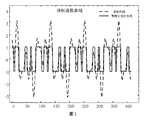
- the dotted line is represented as a modulation function of an SSG.
- the modulation function of the SSG is a continuous periodic function of the simulation. After multiplying the uniform grating, the spatial distribution of the refractive index is also continuously changed, no longer only n h and n l two values, very difficult to make in the process.
- a threshold value is usually selected to perform a two-stage digital discretization process on the continuous function represented by the equation (3).
- the solid line in Figure 1 shows the effect of the super-structured grating modulation function using a threshold V 1 for two-level digital dispersion.
- the discrete envelope function is also periodic for the continuous grating, but the refractive index is still only n.
- the two values h and n l introduce a phase shift only when switching between the envelope functions "1" and "-1", so it is easy to process the SSG.
- the total length of the SSG determines the reflectivity of the reflection peak and the FWHM.
- the total length of the SSG corresponds to a specific reflectivity and FWHM, that is, the reflectance of the reflected peak corresponds to the FWHM. Therefore, for the second-order discrete SSG, the reflectivity and FWHM cannot be independently optimized to achieve performance. Good FWHM and reflectivity.
- the reflectivity and FWHM of the SSG reflection peak are determined by the total length of the SSG, and the SSG reflectance and the FWHM cannot be optimized separately, so that the performance cannot be simultaneously satisfied. Reflectivity and FWHM.
- Embodiments of the present application provide a superstructure grating and a tunable laser for separately optimizing the reflectance of the reflection peak of the superstructure grating and the FWHM, and satisfying the better reflectivity and FWHM.
- the embodiment of the present application provides the following technical solutions:
- an embodiment of the present application provides a superstructure grating that spatially and phase modulates a uniform grating by a modulation function to form a grooming reflection spectrum, and the modulation function is discrete by N thresholds.
- (N+1) modulation function discrete values are obtained, and the N is a positive integer greater than or equal to 2; each of the (N+1) modulation function discrete values corresponds to a segment of refraction
- (N+1) modulation function discrete values are obtained by discretizing the modulation function, and the reflectance of the reflection peak of the super-structure grating is passed through (N+1) modulation function discrete values
- the length of the optical waveguide corresponding to the discrete value of the at least one modulation function is proportional to the total length of the grating of the superstructure grating, and the total length of the grating of the superstructure grating is adjusted.
- the FWHM of the reflection peak of the superstructure grating passes the aforementioned proportional relationship and superstructure.
- the total grating length of the grating is adjusted, that is, the reflectivity of the reflection peak of the superstructure grating and the FWHM can be adjusted by two dimensions.
- the reflectivity of the reflection peak determines the threshold and output power of the tunable laser, and the FWHM of the reflection peak is determined.
- the model selection of the laser the smaller the FWHM, the larger the side mode suppression ratio.
- the tunable laser provided based on the embodiment of the present application can optimize the reflectance and the FWHM separately, so that the better reflectivity and FWHM can be simultaneously satisfied.
- the modulation function performs discretization processing to obtain three discrete values of the modulation function, and the 3
- the discrete values of the modulation functions have a discrete value of the modulation function corresponding to an optical waveguide having a uniform refractive index, and the discrete values of the remaining two modulation functions of the three modulation functions respectively correspond to a uniform grating.
- the discrete values of the three modulation functions corresponding to the optical waveguide and the uniform grating with uniform refractive index can be obtained.
- the reflectivity of the reflection peak of the super-structure grating is discretized by three modulation functions.
- the (N+1) modulation function discrete values have two modulation function discretes
- the values correspond to the same uniform grating.
- a phase shift is added between the optical waveguides corresponding to the discrete values of the adjacent modulation functions.
- a phase shift is cut between the optical waveguides, so that the reflection spectrum of the super-structure grating is flatter, and the reflection performance of the super-structure grating is improved.
- the embodiment of the present application further provides a tunable laser, the tunable laser comprising: a reflective region, wherein the reflective region is configured to pass the superstructure according to any of the foregoing first aspects
- the grating tunes the optical signal.
- Embodiments of the present application also provide a tunable laser based on the aforementioned superstructure grating.
- (N+1) modulation function discrete values are obtained by discretizing the modulation function, and the reflectance of the reflection peak of the super-structure grating is discretized by (N+1) modulation functions.
- the ratio of the length of the optical waveguide corresponding to the discrete value of at least one of the modulation functions to the total length of the grating of the superstructure grating, and the total length of the grating of the superstructure grating are adjusted, and the FWHM of the reflection peak of the superstructure grating passes the aforementioned proportional relationship
- the total length of the grating of the superstructure grating is adjusted, that is, the reflectivity of the reflection peak of the superstructure grating and the FWHM can be adjusted by two dimensions.
- the reflectivity of the reflection peak determines the threshold and output power of the tunable laser, and the reflection peak
- the FWHM determines the model selectivity of the laser. The smaller the FWHM, the larger the side mode suppression ratio.
- the tunable laser provided based on the embodiment of the present application can optimize the reflectance and the FWHM separately, so that the better reflectivity and FWHM can be simultaneously satisfied.
- the tunable laser further includes: a gain region and a phase region, wherein the reflective region includes: a first mirror and a second reflection a mirror; the gain region is respectively cascaded with the first mirror and the phase region through an optical waveguide; the phase region is cascaded with the gain region and the second mirror; the gain region For generating an optical signal; the phase region is for phase adjustment of the optical signal to enable the tunable laser to fine tune a lasing wavelength of the optical signal.
- the generation and phase adjustment of the optical signal can be achieved by the gain and phase regions in the tunable laser, respectively, and the optical signal is transmitted through the reflective region after the lasing wavelength of the optical signal is fine tuned.
- the tunable laser further includes: a semiconductor optical amplifier SOA and a photodetector PD; the first reflection a mirror is cascaded by the optical waveguide and the SOA, the second mirror being cascaded by the optical waveguide and the PD; the SOA for power amplification of the optical signal; the PD, for Power monitoring or power attenuation is performed on the optical signal. Power amplification of the optical signal as well as power monitoring or power attenuation can be achieved by SOA and PD in the tunable laser.
- the tunable laser further includes: a first SOA and a second SOA; the first mirror Cascading through the optical waveguide and the first SOA, the second mirror being cascaded by the optical waveguide and the second SOA; the first SOA, for emitting light to the first mirror The signal is subjected to power amplification; and the second SOA is configured to perform power amplification on the optical signal emitted by the second mirror.
- both the first mirror and the second mirror can be connected to one SOA, and the optical signal emitted by each mirror is power amplified, so that a more powerful optical signal can be emitted.
- the tunable laser further includes: a multimode interference MMI coupler, a gain region, and a phase region;
- the reflective region includes: a first reflection a mirror and a second mirror; one side of the MMI coupler has a port connected to the phase region, and the other side of the MMI coupler has two ports respectively associated with the first mirror and The second mirrors are connected; the two sides of the phase zone are respectively cascaded with the gain zone and one port of the MMI; the gain zone is for generating an optical signal; and the phase zone is for the light The signal is phase adjusted such that the tunable laser is capable of fine tuning the lasing wavelength of the optical signal.
- the MMI coupler is used to couple the light reflected back by the first mirror and the second mirror together into the phase region.
- the active gain region has a lower band gap, corresponding to the target output wavelength of the tunable laser, typically a multiple quantum well, which, when electrically injected, converts electrical energy into light energy to provide gain.
- the tunable laser further includes: a phase adjustment module, wherein the phase adjustment module respectively The MMI coupler, the first mirror connection, or the phase adjustment module is respectively connected to the MMI coupler and the second mirror; the phase adjustment module is configured to match the first mirror The phase between the reflection spectrum and the reflection spectrum of the second mirror. Adding a phase adjustment module on the Y branch arm of the first mirror or the second mirror to match the phase of the reflection spectrum of the two mirrors, so that the first mirror or the second mirror can better pass through the MMI coupler wave.
- the tunable laser further includes: an SOA and a PD; the first mirror has a first port The second mirror has a second port, the gain region has a third port; the first port is connected to the SOA or the PD, and/or the second port is connected to the SOA or The PD, and/or the third port is connected to the SOA or the PD; the SOA is configured to perform power amplification on the optical signal; and the PD is configured to perform power on the optical signal Monitoring or Power attenuation.
- At least one of the first mirror, the second mirror and the gain region may be connected to the SOA through the optical waveguide, and the first mirror, the second mirror and the gain region may be connected to the PD through the optical waveguide, and the tunable laser is integrated SOA and PD can respectively achieve power amplification of optical signals as well as power monitoring or power attenuation.
- the reflective region includes: a heating unit, a transport layer, a mirror, an upper barrier layer, a sacrificial layer, a lower barrier layer, and a substrate layer, wherein the heating unit is located above the transport layer
- the transmission layer is located above the sacrificial layer, and includes, in order from top to bottom, an upper cladding layer, a waveguide layer and a lower cladding layer; the mirror is located in the transmission layer, and the mirror is used to pass The superstructure grating of any of the preceding aspects, wherein the optical signal is tuned; the upper barrier layer is between the transmission layer and the sacrificial layer; and the sacrificial layer is located at the upper barrier layer Between the lower barrier layer, a protective structure is formed in the sacrificial layer, the protective structure and the interlayer region form a hollow structure
- the hollow structure is completely hollow; the transmission layer of the region where the mirror is located and the material of the transmission layer on both sides Between the gaps, a hollow structure is formed over the hollow structure; the voids are periodically arranged along the waveguide direction, the voids penetrating the upper cladding layer, the waveguide layer, the Defining the cladding layer and the upper barrier layer to reach a region where the hollow structure is located, and a support structure between the adjacent gaps for providing lateral mechanical support to the suspended structure, the support structure along the waveguide
- the length period of the direction is not equal to the period of the modulation function of the superstructure grating.
- the area between the corrosion windows is the support area of the suspended structure, and the area between the corrosion windows is not aligned with the peak or valley of the superstructure grating modulation function, ie as long as the peaks are not aligned Or the valleys are not aligned, and the two left and rightmost corrosion windows are used to prevent the temperature from being too low on both sides.
- the transmission layer of the region where the mirror is located is completely isolated from the material of the two sides of the transmission layer to form a gap.
- the void extends through the upper cladding layer, the waveguide layer, the lower cladding layer and the upper barrier layer to reach a region where the hollow structure is located, and a suspended structure is formed above the hollow structure and between the voids
- the bottom of the sacrificial layer is not completely etched, and the sacrificial layer retains a bottom support structure for forming support for the suspended structure.
- the reflective region in the tunable laser can be thermally tuned using a suspended structure to improve the thermal tuning efficiency of the superstructure grating.
- the length of the bottom support structure along the waveguide direction is not equal to the period of the modulation function of the super-structure grating .
- the super-structure grating is located under the upper cladding layer in the transmission layer of the region where the mirror is located a half portion; or, the superstructure grating is located in an upper half of an under cladding layer in a transmission layer of a region where the mirror is located; or, the superstructure grating is located at a waveguide layer in a region where the mirror is located; or The superstructure grating is located in each of the upper cladding layer and the waveguide layer in the transmission layer of the region where the mirror is located; or the superstructure grating is located in the lower cladding layer in the transmission layer of the region where the mirror is located There is a part in each of the waveguide layers.
- the mirror is located in the upper cladding layer for tuning the wavelength of the optical signal.
- the mirror may also be located in the lower cladding layer, or in the waveguide layer, or in the upper cladding layer and the waveguide layer.
- the layers, or in the two layers of the lower cladding layer and the waveguide layer there are various implementations, which are only described herein.
- the optical signal propagates in the upper cladding layer, the lower cladding layer, and the waveguide layer, and the superstructure grating is placed at these positions to reflect the optical signal.
- the refractive index of the waveguide layer is higher than a refractive index of the upper cladding layer and a refractive index of the lower cladding layer . Therefore, when the optical signal propagates in the waveguide layer, total reflection is formed, so that the optical energy can be limited as much as possible in the waveguide layer, so that the waveguide layer can provide a low-loss propagation path of the optical signal and reduce the loss of optical signal propagation.
- the reflective region further includes: an indium phosphide InP buffer layer, wherein The lower barrier layer is located between the sacrificial layer and the InP buffer layer; the InP buffer layer is located between the lower barrier layer and the substrate layer.
- the main function of the InP buffer layer is to provide a better quality crystalline InP material, providing a better material basis for other layer materials.
- 1 is an effect diagram of a modulation function of a superstructure grating in the prior art after two levels of dispersion
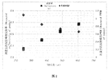
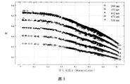
- FIG. 2 is a schematic diagram showing the relationship between the reflectance of the reflection peak and the FWHM and the total length of the SSG of the super-structure grating after the second-stage discretization processing in the prior art;
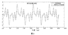
- FIG. 3 is an effect diagram of a modulation function of a super-structure grating in a three-stage discretization process according to an embodiment of the present application
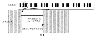
- FIG. 4 is a structural diagram of a super-structure grating after level 3 discretization processing in an embodiment of the present application
- FIG. 5 is a schematic diagram showing the relationship between the reflectance of the super-structured grating after the three-stage discretization processing and the total length of the grating and the portion of the modulation function occupying the total length of the grating in one embodiment of the present application;
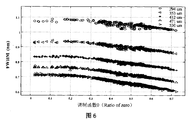
- FIG. 6 is a schematic diagram showing the relationship between the FWHM of the super-structured grating after the 3-level discretization processing and the total length of the grating and the portion of the modulation function occupying the total length of the grating in one embodiment of the present application;
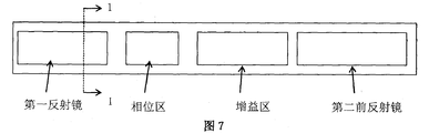
- FIG. 7 is a schematic structural diagram of a tunable laser provided by an embodiment of the present application.
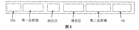
- FIG. 8 is a schematic structural diagram of a tunable laser according to another embodiment of the present application.
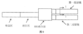
- FIG. 9 is a schematic structural diagram of a tunable laser according to another embodiment of the present application.
- FIG. 10 is a schematic structural diagram of a tunable laser according to another embodiment of the present application.
- FIG. 11 is a top plan view of a suspended structure mirror of a tunable laser provided by an embodiment of the present application.
- Figure 12 is a cross-sectional view of the tunable laser along the 3'-3' position of Figure 11 provided by an embodiment of the present application;
- Figure 13 is a cross-sectional view of the tunable laser along the 4'-4' position of Figure 11 provided by an embodiment of the present application;
- FIG. 14 is a top plan view of a bottom support structure included in a tunable laser provided by an embodiment of the present application;
- Figure 15 is a cross-sectional view of the tunable laser along the 3-3 position of Figure 14 provided by an embodiment of the present application;
- FIG. 16 is a cross-sectional view of the tunable laser along the 1-1 position of FIG. 14 provided by an embodiment of the present application;
- Figure 17 is a cross-sectional view of the tunable laser taken along line 2-2 of Figure 14 provided by an embodiment of the present application.
- the embodiment of the present application provides an independent optimization of the reflectance and FWHM of the reflection peak of the super-structure grating, and at the same time satisfies the better reflectivity and FWHM.
- the three conditions for generating a laser are: achieving particle number inversion, satisfying threshold conditions, and resonance conditions.
- the first condition for generating laser light is the inversion of the number of particles.
- the electrons in the valence band are pumped to the conduction band.
- the heavily doped P-type and N-type materials are usually used to form the PN junction.
- particle number inversion occurs near the junction region, electrons are stored in the high Fermi level, and holes are stored in the low Fermi level, and of course there are many others.
- a method of generating a population inversion Realizing the inversion of the number of particles is a necessary condition for generating laser light, but it is not a sufficient condition.
- the resonance condition refers to the fact that after the length L and the refractive index N of the cavity are determined, only light of a specific frequency can form a light oscillation, and a stable laser is output, which indicates that the cavity has a certain frequency selection effect on the output laser.
- a monolithically integrated semiconductor tunable laser is usually formed by abutting a gain region and an inactive region on an Indium Phosphide (InP) substrate, and its planar schematic is shown in FIG. 7, including a reflection region, a gain region, and a phase adjustment.
- the reflective area may include a first mirror and a second mirror.
- the forbidden band width of the gain region is low, and when the electric injection is performed, the electric energy is converted into light energy to provide a gain;
- the passive region mainly includes a mirror, and the forbidden band width of the passive region is greater than the laser wavelength. The photon energy is higher and the absorption of the laser is small, so it can provide very low absorption loss.
- the passive region may also include a phase adjustment region for fine tuning the effective optical path within the cavity to change the laser output wavelength.
- the two mirrors of the tunable laser have a comb-like reflection spectrum with multiple reflection peaks, and the reflection peaks can be adjusted.
- the output wavelength of the laser can be adjusted by adjusting the reflection peaks.
- the reflectance of the reflection peak and the FWHM are only related to the total length of the grating of the superstructure grating. As shown in FIG.
- the total length of the grating of the superstructure grating in the prior art determines the reflectivity of the reflection peak and FWHM
- the total grating length of the superstructure grating corresponds to a specific reflectivity and FWHM, that is, the reflectance of the reflection peak corresponds to the FWHM one by one, so the reflectivity and FWHM cannot be independently optimized separately to obtain better FWHM and reflection. rate.
- the reflectance of the reflection peak and the FWHM can be adjusted by two dimensions, so that the reflectivity and the FWHM can be independently optimized, so that the reflectivity with better performance can be simultaneously satisfied. And FWHM.
- An embodiment of the present application first provides a superstructure grating which spatially and amplitudeally modulates a uniform grating by a modulation function to form a dressing reflection spectrum, and the modulation function is discretized by N threshold values. Obtaining (N+1) discrete values of the modulation function, N being a positive integer greater than or equal to 2;
- each discrete value of the modulation function corresponds to a section of optical waveguide with uniform refractive index Or corresponding to a uniform grating, the uniform grating is an optical waveguide with alternating high refractive index and low refractive index;
- the reflectance of the reflection peak of the superstructure grating passes through at least one of the discrete values of the (N+1) modulation function discrete values, the length of the optical waveguide corresponding to the total length of the grating of the superstructure grating, and the superstructure grating Adjust the total length of the grating;
- the FWHM of the reflection peak of the superstructure grating is adjusted by the aforementioned proportional relationship and the total length of the grating of the superstructure grating.
- the modulation function of the super-structure grating is discretized by N thresholds to obtain (N+1) discrete values of the modulation function, that is, after the N-level discretization processing of the modulation function of the super-structure grating, (N+ 1) discrete values of the modulation function.
- N discrete values of the modulation function
- two threshold values may be selected to perform three levels of discretization processing on the modulation function of the super-structured grating, and three discrete values of the modulation function may be obtained, which is different from the prior art in which only one threshold is selected for the modulation function.
- the two discrete values of the modulation function are completely different.
- the super-structure grating provided by the embodiment of the present application is exemplified by taking the value of N as 2.
- the super-structure grating provided by the embodiment of the present application can realize the reflectivity and FWHM of the reflection peak respectively, and the discrete values of the three modulation functions can be obtained after the third-order dispersion, and the following formula is an expression of the discrete value of the modulation function Profile_D(z). :
- Threshold1 and Threshold2 are two thresholds.
- the three threshold values of the modulation function Profile(z) are used to obtain three discrete values of the modulation function, as shown in FIG.
- the modulation function of the super-structure grating is subjected to three-stage discretization processing.
- the discrete modulation function has three values of 1,0,-1, so that after the modulation function acts on the uniform grating, the super-structure grating portion corresponding to 1 and -1 still only has high refractive index n h and low refractive index n l For each value, the superstructure grating portion corresponding to 0 has only a high refractive index n h .
- FIG. 4 it is a structural diagram of a super-structure grating after three-stage discretization processing in one embodiment of the present application.
- the modulation function is 1 or -1
- ultra high refractive index gratings low refractive index n h and n l alternating with as uniform grating.
- the superstructure gratings are all high refractive index n h , so that the effective reflection surface is reduced.
- the reflectance of the reflection peak of the superstructure grating can be optimized.
- the morphology of the superstructure grating is magnified and visible, and the shaded portion is a low refractive index portion.
- the superstructure grating has only a high refractive index n h .
- the reflectivity and FWHM of the grating can be adjusted by adjusting the ratio of the 0 portion of the discrete post-modulation function to the total length of the grating of the super-structure grating, and then combining the total length of the grating of the super-structure grating.
- FIG. 5 is a relationship between the reflectance of the super-structured grating after the three-stage discretization processing and the total length of the grating and the proportion of the zero portion of the modulation function to the total length of the grating in one embodiment of the present application.
- FIG. 5 is a relationship between the reflectance of the super-structured grating after the three-stage discretization processing and the total length of the grating and the proportion of the zero portion of the modulation function to the total length of the grating in one embodiment of the present application.
- FIG. 6 is a schematic diagram showing the relationship between the FWHM of the super-structured grating after the three-stage discretization processing and the total length of the grating and the proportion of the zero portion of the modulation function in the total length of the grating in one embodiment of the present application, FIG. 5 and FIG. There are five lines, each corresponding to a super-structured grating of different grating lengths.
- the ratio of the total length of the grating of the optical waveguide corresponding to the modulation function 0 is simply referred to as the ratio of 0 in the modulation function.
- the superstructure grating When the modulation function is 0, the superstructure grating is all n h , so that the effective reflection surface will be By reducing the ratio of the total length of the grating of the optical waveguide corresponding to the modulation function 0, the reflectivity of the superstructure grating can be optimized. If the total length of the grating is longer, the reflectivity is larger. For FWHM, the longer the total length of the grating, the smaller the FWHM, the larger the proportion of the discrete value of the modulation function, and the smaller the FWHM.
- the reflectivity and FWHM of such a superstructure grating are respectively related to the ratio of the total length of the grating and the discrete value of the modulation function of zero.
- the reflectivity and FWHM of the superstructure grating are both related to the total length of the grating and the ratio of 0 in the modulation function, that is, the reflectivity is related to the total length of the grating and the ratio of 0 in the modulation function, FWHM and The total length of the grating and the ratio of 0 in the modulation function are related.
- the reflectivity and FWHM of the superstructure grating can be optimized separately, for example, the total length of the grating is 294 um, and the modulation function is “0”.
- the modulation function is discretized to obtain three discrete values of the modulation function, and the discrete values of the three modulation functions have a modulation function, and the discrete values correspond to a uniform refractive index.
- the discrete values of the three modulation functions of the waveguide and the uniform grating, and the reflectance of the reflection peak of the superstructure grating through one of the discrete values of the three modulation functions, the discrete value of the modulation function corresponding to the refractive index uniformity of the optical waveguide length of the superstructure The proportional relationship of the total length of the grating of the grating, the total length of the grating of the superstructure grating, the reflectivity of the reflected peak, and the FWHM are adjusted to achieve simultaneous optimization of the reflectivity and the FWHM.
- the three discrete values of the modulation function include: a first value, a second value, and a third value, wherein the first value corresponds to a uniform grating, and the second value corresponds to an optical waveguide having a uniform refractive index, The three values correspond to a uniform grating.
- the first value and the third value may be discrete values 1 and -1 of the modulation function shown in FIG. 3, respectively, and the second value may be a discrete value 0 of the modulation function shown in FIG.
- the discrete values of the (N+1) modulation functions have two discrete values of the modulation function corresponding to the same type of uniform grating, and the optical waveguides corresponding to the discrete values of the respective modulation functions in the modulation function are controlled.
- the ratio of the total length of the grating can optimize the reflectivity of the superstructure grating.
- the optical waveguide portion corresponding to the discrete value 0 of the modulation function has only a high refractive index or a low refractive index, so that the super-structure grating does not form a reflective interface when the value of the modulation function is a discrete value of the modulation function 0. .
- the discrete values of the adjacent modulation functions when the sign of the discrete values of the adjacent modulation functions is different or one of the discrete values of the adjacent modulation functions has a discrete value of zero, the discrete values of the adjacent modulation functions respectively correspond to the light
- a phase shift is added between the waveguides, and a phase shift is cut between the optical waveguides when the sign of the modulation function changes, thereby making the reflection spectrum of the superstructure grating flatter and improving the reflection performance of the superstructure grating.
- the three-level discretization processing of the modulation function of the super-structure grating is described by taking the value of N as 2, and the present invention is not limited to the implementation of the present application.
- the modulation function of the superstructure grating provided by the example can also be subjected to 4-level discretization processing, or more advanced discretization processing.
- the super-structure grating can adopt more thresholds, and the modulation function can be higher than or equal to level 4 and the like. Processing.
- the modulation function is 1, -1 or 0 substantially corresponding to different modulation forms of the uniform grating in the super-structure grating, with 4 levels of dispersion
- the discrete value of the modulation function can take 1, 0.5, -0.5, -1, wherein the specific values of the discrete values of the respective modulation functions can be configured according to the application scenario, and only the corresponding modulation forms of the optical waveguides or uniform gratings in which the discrete values of the respective modulation functions are uniform and the values are uniform.
- phase shift is introduced when the sign of the discrete value of the modulation function changes.
- the discrete value of the modulation function can take 1, 0.5, 0, -0.5, -1, etc., for example, "1" "-1" still corresponds to the first uniform grating, 0.5 or -0.5
- 0 corresponds to the optical waveguide with uniform refractive index, when the sign of the discrete values of the adjacent modulation functions is different or one of the discrete values of the adjacent modulation functions has a discrete value of zero. Introduce phase shift.
- the description of the present application shows that the super-structure grating spatially and phase-modulates the uniform grating by a modulation function to form a dressing reflection spectrum, and the modulation function is discretized by N thresholds (N+ 1) discrete values of modulation functions, N is a positive integer greater than or equal to 2, wherein each of the discrete values of (N+1) modulation functions corresponds to an optical waveguide with a uniform refractive index or corresponding
- the uniform grating is an optical waveguide with alternating high refractive index and low refractive index.
- the length of the optical waveguide occupies the ratio of the total length of the grating of the superstructure grating, and the total length of the grating of the superstructure grating is adjusted.
- the FWHM of the reflection peak of the superstructure grating is adjusted by the aforementioned proportional relationship and the total length of the grating of the superstructure grating, that is, The reflectivity and FWHM of the reflection peak of the superstructure grating can be adjusted by two dimensions.
- the reflectivity of the reflection peak determines the threshold and output power of the tunable laser.
- the FWHM of the reflection peak determines the model selectivity of the laser. The more FWHM Small, the side mode suppression ratio is larger.
- the tunable laser provided based on the embodiment of the present application can optimize the reflectance and the FWHM separately, so that the better reflectivity and FWHM can be simultaneously satisfied.
- the foregoing embodiment describes the superstructure grating provided by the present application.
- a tunable laser provided by the present application is described.
- the tunable laser includes: a reflective region, wherein the reflective region is used to pass the superstructure grating in the foregoing embodiment.
- the optical signal is tuned, that is, the embodiment of the present application also provides a tunable laser based on the aforementioned superstructure grating.
- (N+1) modulation function discrete values are obtained by discretizing the modulation function, and the reflectance of the reflection peak of the super-structure grating is discretized by (N+1) modulation functions.
- the ratio of the length of the optical waveguide corresponding to the discrete value of at least one of the modulation functions to the total length of the grating of the superstructure grating, and the total length of the grating of the superstructure grating are adjusted, and the FWHM of the reflection peak of the superstructure grating passes the aforementioned proportional relationship
- the total length of the grating of the superstructure grating is adjusted, that is, the reflectivity of the reflection peak of the superstructure grating and the FWHM can be adjusted by two dimensions.
- the reflectivity of the reflection peak determines the threshold and output power of the tunable laser, and the reflection peak
- the FWHM determines the model selectivity of the laser. The smaller the FWHM, the larger the side mode suppression ratio.
- the tunable laser provided based on the embodiment of the present application can optimize the reflectance and the FWHM separately, so that the better reflectivity and FWHM can be simultaneously satisfied.
- the tunable laser includes a gain region and a phase region, in addition to including a reflective region, wherein
- the reflective area includes: a first mirror and a second mirror
- the gain region is respectively cascaded with the first mirror and the phase region through the optical waveguide;
- the phase region is cascaded with the gain region and the second mirror;
- a phase region for phase adjustment of the optical signal enables the tunable laser to fine tune the lasing wavelength of the optical signal.
- the super-structure grating provided by the foregoing embodiment of the present application may be disposed in the first mirror or may be disposed in the first mirror.
- the positions of the first mirror and the second mirror may be interchanged, for example, the first mirror is a back mirror, and the second mirror is a front mirror.
- the generation and phase adjustment of the optical signal can be achieved by the gain and phase regions in the tunable laser, respectively, and the optical signal is transmitted through the reflective region after the lasing wavelength of the optical signal is fine tuned.
- a schematic diagram of a monolithically integrated tunable laser is composed of a gain section, a first mirror, a second mirror, and a phase section.
- the gain region is located in the active region, and the gain region has a lower band gap, generally a multi-quantum well.
- the electrical energy is converted into light energy to provide a gain.
- the first mirror and the second mirror are equivalent and interchangeable, and the reflection spectra of the first mirror and the second mirror are wavelength selective for wavelength tuning, the first mirror and the second reflection
- the mirror comprises the aforementioned superstructure grating, the reflection spectrum produced by the mirror is a dressing reflection spectrum, and the free spectral range of the first reflection mirror and the second mirror has a certain difference in the free spectral range, and then the two mirrors amplify the tuning range by the cursor effect .
- the phase region provides phase adjustment, so that the laser can finely adjust the lasing wavelength, the light is generated in the gain region, and the first mirror and the second mirror reflect to form a resonance to generate a laser, and then transmit and exit from the first mirror and the second mirror. laser.
- the first mirror, the second mirror and the phase region are all located in the passive region.
- the forbidden band width of the passive region is higher than the photon energy of the laser wavelength, and the absorption of photons is very small, and the passive region can be regenerated by etching.
- the technology etches off the MQW of the active region and then fabricates the compound with a larger band gap by secondary epitaxy.
- both the first mirror and the second mirror can adopt the reflection spectrum of the first mirror and the second mirror of the superstructure grating described in the foregoing embodiments to be wavelength selective for wavelength tuning.
- the phase region, the first mirror, and the second mirror can all be wavelength tuned by electrical injection, or by changing thermal injection, or other equivalent method to change the refractive index of the waveguide.
- the tunable laser further includes: a semiconductor optical amplifier (SOA) and a photo Detector (PD);
- SOA semiconductor optical amplifier
- PD photo Detector
- the first mirror is cascaded by the optical waveguide and the SOA, and the second mirror is cascaded by the optical waveguide and the PD;
- the positions of the first mirror and the second mirror are interchangeable, and the power amplification and power monitoring or power attenuation of the optical signal can be realized by SOA and PD in the tunable laser, and it should be noted that
- the left or right end of the tuned laser can be integrated with SOA for power amplification, or the left or right end of the tunable laser can be integrated with PD for power monitoring or power attenuation.
- the tunable laser further includes: a first SOA and a second SOA;
- the first mirror is cascaded by the optical waveguide and the first SOA
- the second mirror is cascaded by the optical waveguide and the second SOA
- a first SOA configured to perform power amplification on the optical signal emitted by the first mirror
- the second SOA is configured to perform power amplification on the optical signal emitted by the second mirror.
- the first mirror and the second mirror in the tunable laser can be connected to one SOA, and the optical signal emitted by each mirror is power amplified, so that a more powerful optical signal can be emitted.
- the tunable laser further includes: a multi-mode interference (MMI) coupler, a gain region, and a phase region;
- MMI multi-mode interference
- the reflective area includes: a first mirror and a second mirror
- the MMI coupler has one port on one side and is connected to the phase zone. There are two ports on the other side of the MMI coupler. Do not connect to the first mirror and the second mirror.
- phase zone The two sides of the phase zone are respectively cascaded with the gain zone and one port of the MMI;
- a phase region for phase adjustment of the optical signal enables the tunable laser to fine tune the lasing wavelength of the optical signal.
- the tunable laser provided by one embodiment of the present application includes: a gain region, a phase region, an MMI coupler, a first mirror and a second mirror, the MMI coupler is a 1x2 coupler, and has a port on one side, and a phase The zones are coupled, and the other side has two ports, which are first coupled to the mirror and the second mirror, respectively.
- the phase zone is cascaded with the gain zone and the MMI.
- the MMI coupler is used to couple the light reflected back by the first mirror and the second mirror together into the phase region.
- the active gain region has a lower band gap, corresponding to the target output wavelength of the tunable laser, typically a multiple quantum well, which, when electrically injected, converts electrical energy into light energy to provide gain.
- the first mirror and the second mirror can be considered equivalent, the names can be interchanged, and the reflection spectra of the first mirror and the second mirror are wavelength selective for wavelength tuning, for example, first
- the mirror and the second mirror comprise the aforementioned super-structure grating as a dressing reflection spectrum, and the free spectral range of the mirror reflection spectrum of the two mirrors is somewhat different, and the first laser mirror reflected back to the laser cavity of the mirror and the second mirror
- the tuning range is amplified by the MMI combining and then by the additive cursor effect.
- the phase region provides phase adjustment so that the laser can fine tune the lasing wavelength, and the first mirror, the second mirror, and the phase region are all located in the inactive region.
- the phase region, the first mirror, and the second mirror can all be wavelength tuned by electrical injection, or by changing thermal injection, or other equivalent method to change the refractive index of the waveguide.
- the tunable laser further includes: a phase adjustment module, wherein
- the phase adjustment module is respectively connected to the MMI coupler, the first mirror, or the phase adjustment module to the MMI coupler and the second mirror respectively;
- phase adjustment module for matching a phase between a reflection spectrum of the first mirror and a reflection spectrum of the second mirror.
- a phase adjustment module is added on the Y branch arm of the first mirror or the second mirror to match the phase of the reflection spectrum of the two mirrors, so that the first mirror or the second mirror can be better coupled by MMI
- the multiplexed wave is schematically illustrated in FIG. 10 by taking the phase adjustment module on the first mirror as an example.
- the tunable laser further includes: SOA and PD;
- the first mirror has a first port
- the second mirror has a second port
- the gain region has a third port
- the first port is connected to the SOA or PD, and/or the second port is connected to the SOA or PD, and/or the third port is connected to the SOA or PD.
- the integrated SOA and PD can achieve power amplification and power monitoring or power attenuation of the optical signal, respectively.
- the left end of the gain zone is port 1
- the right end of the first mirror is port 2
- the right end of the second mirror is port 3.
- Any one of the three ports can be integrated with SOA to amplify the output optical power, or integrated with PD. Power monitoring or power attenuation.
- FIG. 11 is a top view of a suspended structure mirror of a tunable laser provided by an embodiment of the present application.
- Figure 11 illustrates the principle of the mirror structure of the suspended structure of the tunable laser.
- P1 to P7 are respectively a grating modulation function period, and there are 1 to 6 etching windows above and below the optical waveguide, respectively.
- a support area is provided between two adjacent corrosion windows.
- FIG. 12 a cross-sectional view of a tunable laser along the 3'-3' position in FIG. 11 provided for an embodiment of the present application, as shown in FIG. 13, is an illustration of an embodiment of the present application.
- a cross-sectional view of a tunable laser at 4'-4' position in 11. a reflective region of the tunable laser, comprising: a heating unit, a transport layer, a mirror, an upper barrier layer, a sacrificial layer, a lower barrier layer, and a substrate layer, wherein
- a heating unit located above the transport layer
- the transport layer is located above the sacrificial layer and includes, in order from top to bottom, an upper cladding layer, a waveguide layer and a lower cladding layer;
- a mirror located in the transport layer, for tuning the optical signal by the superstructure grating of any of the preceding claims 1 to 4;
- a sacrificial layer between the upper barrier layer and the lower barrier layer, a protective structure formed in the sacrificial layer, the protective structure and the interlayer region forming a hollow structure, and the interlayer region comprising: a region between the transmission layer and the substrate layer;
- the substrate layer is located below the lower barrier layer.
- the reflective region further includes: an InP buffer layer, wherein the lower barrier layer is between the sacrificial layer and the InP buffer layer; and the InP buffer layer is between the lower barrier layer and the substrate layer.
- the reflective region in the tunable laser can be thermally tuned by a suspended structure to improve the thermal tuning efficiency of the superstructure grating.
- Figure 11 is a schematic view of a reflective region having a suspended structure
- Figures 12 and 13 are schematic views of the 3'-3', 4'-4' cross-sections of Figure 12, respectively.
- the reflective region includes, in order from the bottom to the top, a substrate layer, a lower barrier layer, a sacrificial layer, an upper barrier layer, an under cladding layer, a waveguide layer, an upper cladding layer, and a dielectric layer. Heating layer.
- the advanced discrete superstructure grating is distributed at the interface of the waveguide layer and the upper cladding layer, and the black and white phase portion in Fig. 12 shows a mirror including the superstructure grating.
- the substrate layer is a layer in which the semiconductor crystal needs to be grown on the basis of the crystal substrate, and the substrate layer is located under the lower barrier layer. If an InP buffer layer is also disposed in the reflective region, the InP buffer layer is located between the lower cladding layer and the substrate layer for providing a better crystal quality InP material, providing a better material basis for other layer materials.
- the upper cladding layer, the waveguide layer, and the lower cladding layer are located between the dielectric layer and the InP buffer layer for providing a low loss transmission channel for the optical signal.
- the dielectric layer is used to prevent the heater current from leaking into the upper cladding, the heater can generate heat by the current, the heating layer is used to change the temperature of the mirror region, the heating unit is used to supply heat to the mirror, and the heating resistor can be used.
- the current flows through the heating resistor, which changes the temperature of the heating resistor.
- the arrows below the heater indicate the direction of the heat flow.
- the waveguide layer is made of Indium Gallium Arsenide Phosphide (InGaAsP) material.
- the left and right sides of the sacrificial layer are protective structures, and the protective structures are located on both sides of the upper surface of the lower barrier layer along the propagation direction of the optical signal in the waveguide layer.
- the hollow structure is completely hollow; a gap between the transport layer in the region where the mirror is located and the material on both sides of the transport layer, and a suspended structure between the gaps and the hollow structure;
- the direction is periodically arranged, and the gap extends through the upper cladding layer, the waveguide layer, the lower cladding layer and the upper barrier layer to reach a region where the hollow structure is located, and a support structure is provided between the adjacent gaps for providing lateral mechanical support to the suspended structure.
- the length period of the support structure along the waveguide direction is not equal to the period of the modulation function of the superstructure grating.
- the optical waveguide includes a waveguide layer, which is composed of a waveguide layer and upper and lower cladding layers, and the area in the dotted frame is a preparation process.
- the window for etching the sacrificial layer material, the etchant passes through the windows on both sides of the mirror, respectively etching the sacrificial layer material under the mirror to reach the hollow structure region.
- a region above the hollow structure and between the windows on both sides of the optical waveguide forms a suspended structure as shown in FIGS. 12 and 13.
- a region between the left and right protective structures in the sacrificial layer is a hollow structure, and the gap is from the dielectric layer.
- the waveguide layer After passing through the upper cladding layer, the waveguide layer, the lower cladding layer and the upper barrier layer, it reaches the region where the hollow structure is located. At the same time, in order to avoid the performance of the grating reflection spectrum during thermal tuning, the area between the corrosion windows is the support area of the suspended structure.
- the length of the support structure providing the lateral mechanical support in the waveguide direction is not equal to the period of the modulation function of the superstructure grating, thereby facilitating the deterioration of the flatness of the reflection spectrum of the superstructure grating during thermal tuning, thereby facilitating the adjustment Deterioration of laser performance.
- the period of the length of the support structure along the waveguide direction is not equal to the period of the modulation function of the superstructure grating, and may include the case where the lateral support structure and any one of the specific peaks or troughs in the spatial period of the modulation function of the superstructure grating are misaligned, Improve the reflection flatness of superstructure gratings.
- the peak in the spatial period of the modulation function refers to the maximum value in the spatial period of the modulation function
- the valley in the spatial period of the modulation function refers to the minimum value in the spatial period of the modulation function.
- the reflective region may not be provided with an InP buffer layer, and the lower barrier layer is directly on the substrate layer.
- FIG. 11 the openings shown in FIG. 11 are intended to help those skilled in the art to better understand the embodiments of the present invention, and do not limit the scope of the embodiments of the present invention. It will be obvious to those skilled in the art that various modifications and changes can be made in the shape of the opening in accordance with the example of FIG. 11 which is within the scope of the embodiments of the present invention.
- a tunable laser provided by an embodiment of the present application includes a top view of a bottom support structure.
- the etchant enters the sacrificial layer by the voids to form a hollow structure.
- the transmission layer in the region where the mirror is located is completely isolated from the material of the two sides of the transmission layer to form a gap, and the gap penetrates the upper cladding layer, the waveguide layer, the lower cladding layer and the upper barrier layer to reach the region where the hollow structure is located, above the hollow structure, the gap A suspended structure is formed between them.
- FIG. 14 is a schematic diagram of a reflective region having a suspended structure
- Figure 15 is a cross-sectional view of the tunable laser along the 3-3 position of Figure 14 provided by an embodiment of the present application, from position 3-3 of Figure 14.
- the uncorroded region provides a bottom support structure
- FIG. 16 is a cross-sectional view of the tunable laser along the 1-1 position of FIG.
- FIG. Figure 17 is a cross-sectional view of the tunable laser of position 2-2 of Figure 14 provided with an embodiment of the present application, the sacrificial layer of the tunable laser is not completely etched, leaving a bottom support structure to provide the hollow structure Bottom support.
- Figure 14 there are some periodic dashed boxes on both sides of the optical waveguide.
- the area inside the dotted frame is the window used to etch the sacrificial layer material during the preparation process.
- the etchant passes through the windows on both sides of the mirror and is respectively engraved.
- the sacrificial layer material under the mirror is etched to form a suspended structure.
- Figure 11 utilizes a lateral support structure for lateral mechanical support of the suspended structure.
- the sacrificial layer under the suspended structure is not completely etched, and some pillars are formed.
- the bottom of the suspended structure is supported by the bottom of the suspended structure.
- the length of the bottom support structure along the waveguide direction is not equal to the period of the modulation function of the superstructure grating, thereby being thermally tuned It is advantageous to avoid deterioration of the flatness of the reflection spectrum of the super-structure grating, thereby facilitating the deterioration of the performance of the tunable laser.
- the length of the bottom support structure along the waveguide direction is not equal to the period of the modulation function of the super-structure grating, and may specifically include the case where the bottom support structure and any one of the specific peaks or troughs of the modulation function space period of the super-structure grating are misaligned, The reflection flatness of the superstructure grating can be improved.
- the peak in the spatial period of the modulation function refers to the maximum value in the spatial period of the modulation function
- the valley in the spatial period of the modulation function refers to the minimum value in the spatial period of the modulation function.
- the superstructure grating is located in the lower half of the upper cladding layer in the transmission layer of the region where the mirror is located;
- the superstructure grating is located in the upper half of the lower cladding layer in the transport layer of the region where the mirror is located;
- the superstructure grating is located in the waveguide layer in the transport layer of the region where the mirror is located;
- the superstructure grating is located in each of the upper cladding layer and the waveguide layer in the transmission layer of the region where the mirror is located; or
- the superstructure grating is located in a portion of the lower cladding layer and the waveguide layer in the transmission layer of the region where the mirror is located.
- the mirror is located in the upper cladding layer for tuning the wavelength of the optical signal.
- the mirror may also be located in the lower cladding layer, or in the waveguide layer, or on the upper layer.
- the two layers of the cladding layer and the waveguide layer, or in the two layers of the lower cladding layer and the waveguide layer there are various implementations, which are only described herein.
- the optical signal propagates in the upper cladding layer, the lower cladding layer, and the waveguide layer, and the superstructure grating is placed at these positions to reflect the optical signal.
- the refractive index of the waveguide layer is higher than the refractive index of the upper cladding layer and the refractive index of the lower cladding layer. Therefore, when the optical signal propagates in the waveguide layer, total reflection is formed, so that the optical energy can be limited as much as possible in the waveguide layer, so that the waveguide layer can provide a low-loss propagation path of the optical signal and reduce the loss of optical signal propagation.
- the reflectivity of the grating reflection peak determines the threshold value of the tunable laser, the output power and the like, and the FWHM of the grating reflection peak determines the model selectivity of the laser (FWHM defines the reflection peak). Sharpness), the smaller the theoretical FWHM is, the larger the side mode suppression ratio is. The ideal way is to optimize the two separately.
- the embodiment of the present application proposes a three-level discrete or even higher-level discrete super-structure grating, and optimizes the reflection of the reflected peak by adjusting the length of the grating and the ratio of the optical waveguide corresponding to the discrete value of the modulation function to the total length of the grating of the super-structure grating.
- Embodiments of the present application simultaneously propose a plurality of tunable lasers based on advanced discrete gratings, and a mirror structure for improving the thermal tuning efficiency of advanced discrete gratings, and improving the tuning efficiency by etching a sacrificial layer to form a suspended structure, and the bottom support structure is used for Mechanical support is provided to the suspended structure to ensure a fixed position of the suspended structure in the tunable laser.
Landscapes
- Physics & Mathematics (AREA)
- Optics & Photonics (AREA)
- General Physics & Mathematics (AREA)
- Electromagnetism (AREA)
- Condensed Matter Physics & Semiconductors (AREA)
- Engineering & Computer Science (AREA)
- Computer Networks & Wireless Communication (AREA)
- Signal Processing (AREA)
- Semiconductor Lasers (AREA)
- Optical Integrated Circuits (AREA)
- Optical Modulation, Optical Deflection, Nonlinear Optics, Optical Demodulation, Optical Logic Elements (AREA)
Abstract
Description


Claims (18)
- 一种超结构光栅,其特征在于,所述超结构光栅通过调制函数对均匀光栅在空间上进行幅度和相位调制从而形成梳妆反射谱,所述调制函数通过N个阈值进行离散化处理后得到(N+1)个调制函数离散值,所述N为大于或等于2的正整数;所述(N+1)个调制函数离散值中每个调制函数离散值对应于一段折射率均匀不变的光波导或对应于一段均匀光栅,所述均匀光栅为高折射率和低折射率交替变化的光波导;所述超结构光栅的反射峰的反射率通过所述(N+1)个调制函数离散值中的至少一个调制函数离散值所对应的光波导长度占所述超结构光栅的光栅总长度的比例关系、所述超结构光栅的光栅总长度进行调节;所述超结构光栅的反射峰的半高全宽FWHM通过所述比例关系、所述超结构光栅的光栅总长度进行调节。
- 根据权利要求1所述的超结构光栅,其特征在于,当所述N的取值为2时,所述调制函数进行离散化处理后得到3个调制函数离散值,所述3个调制函数离散值有一个调制函数离散值对应一段折射率均匀不变的光波导,所述3个调制函数离散值中其余两个调制函数离散值分别对应于一段均匀光栅。
- 根据权利要求1或2所述的超结构光栅,其特征在于,所述(N+1)个调制函数离散值中存在两个调制函数离散值对应于同一种的均匀光栅。
- 根据权利要求1或2所述的超结构光栅,其特征在于,当相邻的调制函数离散值的正负号不同或者所述相邻的调制函数离散值中有一个离散值为零时,所述相邻的调制函数离散值分别对应的光波导之间加入有相移。
- 一种可调谐激光器,其特征在于,所述可调谐激光器包括:反射区,其中,所述反射区,用于通过如权利要求1至4中任一项所述的超结构光栅对光信号进行调谐。
- 根据权利要求5所述的可调谐激光器,其特征在于,所述可调谐激光器,还包括:增益区和相位区,其中;所述反射区包括:第一反射镜和第二反射镜;所述增益区通过光波导分别和所述第一反射镜、所述相位区进行级联;所述相位区与所述增益区、所述第二反射镜相级联;所述增益区,用于产生光信号;所述相位区,用于对所述光信号进行相位调节,使所述可调谐激光器能够微调所述光信号的激射波长。
- 根据权利要求6的可调谐激光器,其特征在于,所述可调谐激光器,还包括:半导体光放大器SOA和光探测器PD;所述第一反射镜通过光波导和所述SOA进行级联,所述第二反射镜通过光波导和所述PD进行级联;所述SOA,用于对所述光信号进行功率放大;所述PD,用于对所述光信号进行功率监测或功率衰减。
- 根据权利要求6所述的可调谐激光器,其特征在于,所述可调谐激光器,还包括: 第一SOA和第二SOA;所述第一反射镜通过光波导和所述第一SOA进行级联,所述第二反射镜通过光波导和所述第二SOA进行级联;所述第一SOA,用于对所述第一反射镜射出的光信号进行功率放大;所述第二SOA,用于对所述第二反射镜射出的光信号进行功率放大。
- 根据权利要求5所述的可调谐激光器,其特征在于,所述可调谐激光器,还包括:多模干涉MMI耦合器、增益区和相位区;所述反射区包括:第一反射镜和第二反射镜;所述MMI耦合器的一侧有一个端口,与所述相位区相连接,所述MMI耦合器的另一侧有两个端口,分别与所述第一反射镜和所述第二反射镜相连接;所述相位区两侧分别与增益区和MMI的一个端口相级联;所述增益区,用于产生光信号;所述相位区,用于对所述光信号进行相位调节,使所述可调谐激光器能够微调所述光信号的激射波长。
- 根据权利要求9的可调谐激光器,其特征在于,所述可调谐激光器,还包括:相位调整模块,其中,所述相位调整模块分别和所述MMI耦合器、所述第一反射镜连接,或所述相位调整模块分别和所述MMI耦合器、所述第二反射镜连接;所述相位调整模块,用于匹配所述第一反射镜的反射谱和所述第二反射镜的反射谱之间的相位。
- 根据权利要求9的可调谐激光器,其特征在于,所述可调谐激光器,还包括:SOA和PD;所述第一反射镜具有第一端口,所述第二反射镜具有第二端口,所述增益区具有第三端口;所述第一端口连接有所述SOA或所述PD,和/或所述第二端口连接有所述SOA或所述PD,和/或所述第三端口连接有所述SOA或所述PD;所述SOA,用于对所述光信号进行功率放大;所述PD,用于对所述光信号进行功率监测或功率衰减。
- 根据权利要求5至11的可调谐激光器,其特征在于,所述反射区,包括:加热单元、传输层、反射镜、上阻挡层、牺牲层、下阻挡层和衬底层,其中,所述加热单元,位于所述传输层的上方;所述传输层,位于所述牺牲层上方,从上到下依次包括:上包层、波导层和下包层;所述反射镜,位于所述传输层中,所述反射镜用于通过前述权利要求1至4中任一项所述的超结构光栅对光信号进行调谐;所述上阻挡层,位于所述传输层和所述牺牲层之间;所述牺牲层,位于所述上阻挡层和下阻挡层之间,所述牺牲层内形成有保护结构,所述保护结构与层间区域形成中空结构,所述层间区域包括:所述传输层与所述下阻挡层之间的区域;所述下阻挡层,位于所述牺牲层和所述衬底层之间;所述衬底层,位于所述牺牲层的下方。
- 根据权利要求12所述的可调谐激光器,其特征在于,所述中空结构为完全空心;所述反射镜所在区域的传输层与两侧传输层材料之间具有空隙,在所述空隙之间、所述中空结构之上形成悬空结构;所述空隙沿着波导方向周期性排布,所述空隙贯穿所述上包层、所述波导层、所述下包层和所述上阻挡层之后到达所述中空结构所在区域,相邻的所述空隙之间有支撑结构,用于对所述悬空结构提供侧向机械支撑,所述支撑结构沿波导方向的长度周期不等于所述超结构光栅的调制函数的周期。
- 根据权利要求12所述的可调谐激光器,其特征在于,所述反射镜所在区域的传输层与两侧传输层材料之间完全隔离开形成空隙,所述空隙贯穿所述上包层、所述波导层、所述下包层和所述上阻挡层之后到达所述中空结构所在区域,在所述中空结构上方、所述空隙之间形成悬空结构;所述牺牲层中底部没有被完全腐蚀,所述牺牲层保留有底部支撑结构,所述底部支撑结构用于对所述悬空结构形成支撑。
- 根据权利要求14所述的可调谐激光器,其特征在于,所述底部支撑结构沿波导方向的长度周期不等于所述超结构光栅的调制函数的周期。
- 根据权利要求12所述的可调谐激光器,其特征在于,所述超结构光栅位于所述反射镜所在区域的传输层中的上包层的下半部分;或,所述超结构光栅位于所述反射镜所在区域的传输层中的下包层的上半部分;或,所述超结构光栅位于所述反射镜所在区域的波导层;或,所述超结构光栅位于所述反射镜所在区域的传输层中的上包层和波导层中各存在一部分;或,所述超结构光栅位于所述反射镜所在区域的传输层中的下包层和波导层中各存在一部分。
- 根据权利要求12所述的可调谐激光器,其特征在于,所述波导层的折射率高于上包层的折射率和下包层的折射率。
- 根据权利要求12至17中任一项所述的可调谐激光器,其特征在于,所述反射区,还包括:磷化铟InP缓冲层,其中,所述下阻挡层,位于所述牺牲层和所述InP缓冲层之间;所述InP缓冲层,位于所述下阻挡层和所述衬底层之间。
Priority Applications (3)
| Application Number | Priority Date | Filing Date | Title |
|---|---|---|---|
| JP2020505957A JP2020517122A (ja) | 2017-04-17 | 2017-11-21 | 超周期構造回折格子および波長可変レーザ |
| EP17905992.8A EP3605159B1 (en) | 2017-04-17 | 2017-11-21 | Super structure grating and tunable laser |
| US16/656,219 US10931085B2 (en) | 2017-04-17 | 2019-10-17 | Super structure grating and tunable laser |
Applications Claiming Priority (2)
| Application Number | Priority Date | Filing Date | Title |
|---|---|---|---|
| CN201710247396.3A CN108732667B (zh) | 2017-04-17 | 2017-04-17 | 一种超结构光栅和可调谐激光器 |
| CN201710247396.3 | 2017-04-17 |
Related Child Applications (1)
| Application Number | Title | Priority Date | Filing Date |
|---|---|---|---|
| US16/656,219 Continuation US10931085B2 (en) | 2017-04-17 | 2019-10-17 | Super structure grating and tunable laser |
Publications (1)
| Publication Number | Publication Date |
|---|---|
| WO2018192220A1 true WO2018192220A1 (zh) | 2018-10-25 |
Family
ID=63856365
Family Applications (1)
| Application Number | Title | Priority Date | Filing Date |
|---|---|---|---|
| PCT/CN2017/112142 Ceased WO2018192220A1 (zh) | 2017-04-17 | 2017-11-21 | 一种超结构光栅和可调谐激光器 |
Country Status (5)
| Country | Link |
|---|---|
| US (1) | US10931085B2 (zh) |
| EP (1) | EP3605159B1 (zh) |
| JP (1) | JP2020517122A (zh) |
| CN (1) | CN108732667B (zh) |
| WO (1) | WO2018192220A1 (zh) |
Families Citing this family (6)
| Publication number | Priority date | Publication date | Assignee | Title |
|---|---|---|---|---|
| CN108879309B (zh) * | 2017-05-09 | 2021-02-12 | 华为技术有限公司 | 用于可调激光器的反射镜结构和可调激光器 |
| CN114128061B (zh) * | 2019-08-06 | 2024-07-30 | 华为技术有限公司 | 一种波导结构、集成光芯片及实现电学隔离的方法 |
| JP7481653B2 (ja) * | 2020-10-13 | 2024-05-13 | 日本電信電話株式会社 | 波長可変光源およびその制御方法 |
| CN114764163B (zh) * | 2021-01-15 | 2024-07-30 | 宁波元芯光电子科技有限公司 | 一种悬空波导支撑结构及其制作方法 |
| WO2022254687A1 (ja) * | 2021-06-04 | 2022-12-08 | 三菱電機株式会社 | 半導体光集積素子及び光集積装置 |
| US11609392B1 (en) * | 2022-02-24 | 2023-03-21 | X Development Llc | Photonic coupler |
Citations (6)
| Publication number | Priority date | Publication date | Assignee | Title |
|---|---|---|---|---|
| US5715271A (en) * | 1996-08-01 | 1998-02-03 | Northern Telecom Limited | Polarization independent grating resonator filter |
| US20030007524A1 (en) * | 2001-07-04 | 2003-01-09 | Mitsubishi Denki Kabushiki Kaisha | Variable wavelength semiconductor laser and optical module |
| US20040125833A1 (en) * | 1999-05-17 | 2004-07-01 | Interuniversitair Microelektronica Centrum | Widely wavelength tunable integrated semiconductor device and method for widely wavelength tuning semiconductor devices |
| CN101022206A (zh) * | 2007-03-15 | 2007-08-22 | 华中科技大学 | 一种可调谐半导体激光器 |
| US20120027041A1 (en) * | 2009-03-16 | 2012-02-02 | Hiroyuki Yamazaki | Wavelength variable laser and a manufacturing method thereof |
| CN102074892B (zh) * | 2010-12-07 | 2012-02-22 | 北京邮电大学 | 可调谐半导体激光器的制作方法 |
Family Cites Families (34)
| Publication number | Priority date | Publication date | Assignee | Title |
|---|---|---|---|---|
| US4468766A (en) * | 1982-09-30 | 1984-08-28 | The United States Of America As Represented By The Secretary Of The Navy | Optical RF downconverter |
| CA2228683C (en) * | 1998-02-20 | 2002-05-14 | Ivan Avrutsky | Superimposed grating wdm tunable lasers |
| JP4690521B2 (ja) * | 1999-05-17 | 2011-06-01 | アイメック | 広い範囲の波長で同調可能な集積化された半導体装置及び広い範囲の波長で同調可能な半導体装置のための方法 |
| AU2002226036A1 (en) * | 2000-11-06 | 2002-05-15 | Cidra Corporation | Compression-tuned bragg grating-based laser |
| US7356224B2 (en) * | 2001-07-03 | 2008-04-08 | Brown University Research Foundation | Method and apparatus for detecting multiple optical wave lengths |
| US20040174915A1 (en) * | 2002-09-18 | 2004-09-09 | Adc Telecommunications, Inc. | Method for characterizing tunable lasers |
| JP2005003805A (ja) * | 2003-06-10 | 2005-01-06 | Sumitomo Electric Ind Ltd | 光導波路型回折格子素子製造方法および装置 |
| US7627006B2 (en) * | 2003-09-18 | 2009-12-01 | Universite Laval | Multi-wavelength laser source |
| US7636522B2 (en) * | 2004-04-15 | 2009-12-22 | Infinera Corporation | Coolerless photonic integrated circuits (PICs) for WDM transmission networks and PICs operable with a floating signal channel grid changing with temperature but with fixed channel spacing in the floating grid |
| CN100345013C (zh) * | 2004-11-19 | 2007-10-24 | 东南大学 | 含有光波导内嵌入式倾斜布拉格光栅的装置及光处理方法 |
| GB2430760A (en) * | 2005-09-29 | 2007-04-04 | Bookham Technology Plc | Chirped Bragg grating structure |
| US7738527B2 (en) * | 2005-12-30 | 2010-06-15 | Jian-Jun He | Wavelength switchable semiconductor laser using half-wave coupled active double-ring resonator |
| US20080089698A1 (en) * | 2006-05-19 | 2008-04-17 | Zhi Jiang | Optical arbitrary waveform generation and processing using spectral line-by-line pulse shaping |
| JP5407526B2 (ja) * | 2009-04-27 | 2014-02-05 | 住友電気工業株式会社 | 波長可変レーザ、波長可変レーザ装置、及び波長可変レーザ制御方法 |
| US8867578B2 (en) * | 2009-10-13 | 2014-10-21 | Skorpios Technologies, Inc. | Method and system for hybrid integration of a tunable laser for a cable TV transmitter |
| WO2011046898A1 (en) * | 2009-10-13 | 2011-04-21 | Skorpios Technologies, Inc. | Method and system for hybrid integration of a tunable laser |
| US8559470B2 (en) * | 2009-10-13 | 2013-10-15 | Skorpios Technologies, Inc. | Method and system for hybrid integration of a tunable laser and a phase modulator |
| CN101794952B (zh) * | 2010-01-27 | 2011-06-22 | 中国科学院半导体研究所 | 低相位噪声窄线宽可精确调谐光纤化激光微波源 |
| EP2539979B1 (en) * | 2010-02-24 | 2018-05-23 | Universiteit Gent | Laser light coupling into SOI CMOS photonic integrated circuit |
| US8670476B2 (en) * | 2010-09-14 | 2014-03-11 | The Board Of Trustees Of The University Of Illinois | Distributed reflector in a microring resonator |
| CN102412504B (zh) * | 2011-11-25 | 2013-06-12 | 李若林 | 基于相位耦合反射光栅反馈的波长可调谐激光器 |
| US9606273B2 (en) * | 2012-01-11 | 2017-03-28 | Lumentum Operations Llc | Diffractive MEMS device |
| CN102646926B (zh) * | 2012-04-11 | 2013-09-25 | 四川马尔斯科技有限责任公司 | 基于复合mzi及反射光栅的波长可调谐激光器 |
| CN103219649A (zh) * | 2012-06-25 | 2013-07-24 | 四川马尔斯科技有限责任公司 | 直接高速调制外腔式波长可调谐激光器 |
| US8861556B2 (en) * | 2012-07-05 | 2014-10-14 | Jds Uniphase Corporation | Tunable Bragg grating and a tunable laser diode using same |
| GB2507527A (en) * | 2012-11-01 | 2014-05-07 | Oclaro Technology Ltd | Semiconductor DBR laser |
| EP2997632B1 (en) * | 2013-05-21 | 2019-03-20 | Huawei Technologies Co., Ltd. | Laser with full c-band tunability and narrow linewidth |
| WO2015013651A2 (en) * | 2013-07-26 | 2015-01-29 | The General Hospital Corporation | System, apparatus and method utilizing optical dispersion for fourier-domain optical coherence tomography |
| JP2015170750A (ja) * | 2014-03-07 | 2015-09-28 | 住友電気工業株式会社 | 光半導体素子及び光半導体素子の製造方法 |
| CN104104011A (zh) * | 2014-08-08 | 2014-10-15 | 武汉光迅科技股份有限公司 | 一种宽带可调谐激光器 |
| JP6684094B2 (ja) * | 2015-03-20 | 2020-04-22 | 古河電気工業株式会社 | 波長可変レーザ素子およびレーザモジュール |
| WO2017147397A1 (en) * | 2016-02-26 | 2017-08-31 | The Regents Of The University Of California | Comb assisted spread-spectrum receiver and reception methods |
| CN108879309B (zh) * | 2017-05-09 | 2021-02-12 | 华为技术有限公司 | 用于可调激光器的反射镜结构和可调激光器 |
| US10720993B2 (en) * | 2018-05-11 | 2020-07-21 | Government Of The United States Of America, As Represented By The Secretary Of Commerce | Metasurface optical pulse shaper for shaping an optical pulse in a temporal domain |
-
2017
- 2017-04-17 CN CN201710247396.3A patent/CN108732667B/zh active Active
- 2017-11-21 WO PCT/CN2017/112142 patent/WO2018192220A1/zh not_active Ceased
- 2017-11-21 JP JP2020505957A patent/JP2020517122A/ja active Pending
- 2017-11-21 EP EP17905992.8A patent/EP3605159B1/en active Active
-
2019
- 2019-10-17 US US16/656,219 patent/US10931085B2/en active Active
Patent Citations (6)
| Publication number | Priority date | Publication date | Assignee | Title |
|---|---|---|---|---|
| US5715271A (en) * | 1996-08-01 | 1998-02-03 | Northern Telecom Limited | Polarization independent grating resonator filter |
| US20040125833A1 (en) * | 1999-05-17 | 2004-07-01 | Interuniversitair Microelektronica Centrum | Widely wavelength tunable integrated semiconductor device and method for widely wavelength tuning semiconductor devices |
| US20030007524A1 (en) * | 2001-07-04 | 2003-01-09 | Mitsubishi Denki Kabushiki Kaisha | Variable wavelength semiconductor laser and optical module |
| CN101022206A (zh) * | 2007-03-15 | 2007-08-22 | 华中科技大学 | 一种可调谐半导体激光器 |
| US20120027041A1 (en) * | 2009-03-16 | 2012-02-02 | Hiroyuki Yamazaki | Wavelength variable laser and a manufacturing method thereof |
| CN102074892B (zh) * | 2010-12-07 | 2012-02-22 | 北京邮电大学 | 可调谐半导体激光器的制作方法 |
Non-Patent Citations (1)
| Title |
|---|
| See also references of EP3605159A4 |
Also Published As
| Publication number | Publication date |
|---|---|
| JP2020517122A (ja) | 2020-06-11 |
| US10931085B2 (en) | 2021-02-23 |
| EP3605159A1 (en) | 2020-02-05 |
| CN108732667A (zh) | 2018-11-02 |
| EP3605159B1 (en) | 2025-07-30 |
| US20200052467A1 (en) | 2020-02-13 |
| CN108732667B (zh) | 2021-01-05 |
| EP3605159A4 (en) | 2020-04-22 |
Similar Documents
| Publication | Publication Date | Title |
|---|---|---|
| US6597497B2 (en) | Semiconductor optical amplifier with transverse laser cavity intersecting optical signal path and method of fabrication thereof | |
| WO2018192220A1 (zh) | 一种超结构光栅和可调谐激光器 | |
| US7265898B2 (en) | Semiconductor optical amplifier using laser cavity energy to amplify signal and method of fabrication thereof | |
| US10666014B2 (en) | Tunable laser and manufacturing method for tunable laser | |
| US7796656B2 (en) | Enhanced efficiency laterally-coupled distributed feedback laser | |
| US7126731B1 (en) | Optical latch based on lasing semiconductor optical amplifiers | |
| Menon et al. | Control of quality factor and critical coupling in microring resonators through integration of a semiconductor optical amplifier | |
| US20100245990A1 (en) | Semiconductor optical amplifier and optical module | |
| WO2013069483A1 (ja) | 集積型半導体レーザ素子 | |
| JPH08213684A (ja) | 同調可能なレーザ装置 | |
| CA2965235A1 (en) | External cavity laser comprising a photonic crystal resonator | |
| US9071038B2 (en) | Segmented distributed feedback laser | |
| CN110376766B (zh) | 一种反射装置及可调谐激光器 | |
| WO2020147828A1 (zh) | 可调谐激光器 | |
| Nowell et al. | Low-chirp and enhanced-resonant frequency by direct push-pull modulation of DFB lasers | |
| JP4321970B2 (ja) | 半導体光増幅器およびase放射用光源装置および光ゲートアレイおよび波長可変レーザ装置および多波長レーザ装置および光伝送システム | |
| Komljenovic et al. | Narrow linewidth tunable laser using coupled resonator mirrors | |
| JP2007219561A (ja) | 半導体発光装置 | |
| US11557876B2 (en) | Semiconductor laser | |
| JP2005249973A (ja) | 波長フィルタ及び波長可変フィルタ | |
| Suzuki et al. | Wide-tuning (65 nm) semi-cooled (50 C) operation of a tunable laser based on a novel widely tunable filter | |
| JP2019522379A (ja) | 分布帰還型レーザーダイオード | |
| RU184264U1 (ru) | Инжекционный лазер с переключаемым спектром генерации | |
| US20240396299A1 (en) | Semiconductor Laser | |
| Sato et al. | A compact external cavity wavelength tunable laser without an intracavity etalon |
Legal Events
| Date | Code | Title | Description |
|---|---|---|---|
| 121 | Ep: the epo has been informed by wipo that ep was designated in this application |
Ref document number: 17905992 Country of ref document: EP Kind code of ref document: A1 |
|
| ENP | Entry into the national phase |
Ref document number: 2020505957 Country of ref document: JP Kind code of ref document: A |
|
| NENP | Non-entry into the national phase |
Ref country code: DE |
|
| ENP | Entry into the national phase |
Ref document number: 2017905992 Country of ref document: EP Effective date: 20191024 |
|
| WWG | Wipo information: grant in national office |
Ref document number: 2017905992 Country of ref document: EP |