WO2018198538A1 - アーク抑制装置、移動体及び電力供給システム - Google Patents
アーク抑制装置、移動体及び電力供給システム Download PDFInfo
- Publication number
- WO2018198538A1 WO2018198538A1 PCT/JP2018/008627 JP2018008627W WO2018198538A1 WO 2018198538 A1 WO2018198538 A1 WO 2018198538A1 JP 2018008627 W JP2018008627 W JP 2018008627W WO 2018198538 A1 WO2018198538 A1 WO 2018198538A1
- Authority
- WO
- WIPO (PCT)
- Prior art keywords
- power
- limiting circuit
- current limiting
- arc suppression
- power source
- Prior art date
- Legal status (The legal status is an assumption and is not a legal conclusion. Google has not performed a legal analysis and makes no representation as to the accuracy of the status listed.)
- Ceased
Links
Images



Classifications
-
- H—ELECTRICITY
- H01—ELECTRIC ELEMENTS
- H01H—ELECTRIC SWITCHES; RELAYS; SELECTORS; EMERGENCY PROTECTIVE DEVICES
- H01H9/00—Details of switching devices, not covered by groups H01H1/00 - H01H7/00
- H01H9/54—Circuit arrangements not adapted to a particular application of the switching device and for which no provision exists elsewhere
- H01H9/541—Contacts shunted by semiconductor devices
- H01H9/542—Contacts shunted by static switch means
-
- H—ELECTRICITY
- H01—ELECTRIC ELEMENTS
- H01H—ELECTRIC SWITCHES; RELAYS; SELECTORS; EMERGENCY PROTECTIVE DEVICES
- H01H9/00—Details of switching devices, not covered by groups H01H1/00 - H01H7/00
- H01H9/54—Circuit arrangements not adapted to a particular application of the switching device and for which no provision exists elsewhere
-
- B—PERFORMING OPERATIONS; TRANSPORTING
- B60—VEHICLES IN GENERAL
- B60R—VEHICLES, VEHICLE FITTINGS, OR VEHICLE PARTS, NOT OTHERWISE PROVIDED FOR
- B60R16/00—Electric or fluid circuits specially adapted for vehicles and not otherwise provided for; Arrangement of elements of electric or fluid circuits specially adapted for vehicles and not otherwise provided for
- B60R16/02—Electric or fluid circuits specially adapted for vehicles and not otherwise provided for; Arrangement of elements of electric or fluid circuits specially adapted for vehicles and not otherwise provided for electric constitutive elements
-
- H—ELECTRICITY
- H01—ELECTRIC ELEMENTS
- H01H—ELECTRIC SWITCHES; RELAYS; SELECTORS; EMERGENCY PROTECTIVE DEVICES
- H01H33/00—High-tension or heavy-current switches with arc-extinguishing or arc-preventing means
- H01H33/02—Details
- H01H33/59—Circuit arrangements not adapted to a particular application of the switch and not otherwise provided for, e.g. for ensuring operation of the switch at a predetermined point in the AC cycle
-
- H—ELECTRICITY
- H01—ELECTRIC ELEMENTS
- H01H—ELECTRIC SWITCHES; RELAYS; SELECTORS; EMERGENCY PROTECTIVE DEVICES
- H01H47/00—Circuit arrangements not adapted to a particular application of the relay and designed to obtain desired operating characteristics or to provide energising current
-
- H—ELECTRICITY
- H01—ELECTRIC ELEMENTS
- H01H—ELECTRIC SWITCHES; RELAYS; SELECTORS; EMERGENCY PROTECTIVE DEVICES
- H01H73/00—Protective overload circuit-breaking switches in which excess current opens the contacts by automatic release of mechanical energy stored by previous operation of a hand reset mechanism
- H01H73/02—Details
- H01H73/18—Means for extinguishing or suppressing arc
-
- H—ELECTRICITY
- H01—ELECTRIC ELEMENTS
- H01H—ELECTRIC SWITCHES; RELAYS; SELECTORS; EMERGENCY PROTECTIVE DEVICES
- H01H85/00—Protective devices in which the current flows through a part of fusible material and this current is interrupted by displacement of the fusible material when this current becomes excessive
- H01H85/02—Details
- H01H85/46—Circuit arrangements not adapted to a particular application of the protective device
-
- H—ELECTRICITY
- H01—ELECTRIC ELEMENTS
- H01H—ELECTRIC SWITCHES; RELAYS; SELECTORS; EMERGENCY PROTECTIVE DEVICES
- H01H9/00—Details of switching devices, not covered by groups H01H1/00 - H01H7/00
- H01H9/54—Circuit arrangements not adapted to a particular application of the switching device and for which no provision exists elsewhere
- H01H9/547—Combinations of mechanical switches and static switches, the latter being controlled by the former
-
- H—ELECTRICITY
- H01—ELECTRIC ELEMENTS
- H01R—ELECTRICALLY-CONDUCTIVE CONNECTIONS; STRUCTURAL ASSOCIATIONS OF A PLURALITY OF MUTUALLY-INSULATED ELECTRICAL CONNECTING ELEMENTS; COUPLING DEVICES; CURRENT COLLECTORS
- H01R13/00—Details of coupling devices of the kinds covered by groups H01R12/70 or H01R24/00 - H01R33/00
- H01R13/66—Structural association with built-in electrical component
- H01R13/70—Structural association with built-in electrical component with built-in switch
- H01R13/703—Structural association with built-in electrical component with built-in switch operated by engagement or disengagement of coupling parts, e.g. dual-continuity coupling part
-
- H—ELECTRICITY
- H02—GENERATION; CONVERSION OR DISTRIBUTION OF ELECTRIC POWER
- H02H—EMERGENCY PROTECTIVE CIRCUIT ARRANGEMENTS
- H02H3/00—Emergency protective circuit arrangements for automatic disconnection directly responsive to an undesired change from normal electric working condition with or without subsequent reconnection ; integrated protection
- H02H3/08—Emergency protective circuit arrangements for automatic disconnection directly responsive to an undesired change from normal electric working condition with or without subsequent reconnection ; integrated protection responsive to excess current
- H02H3/087—Emergency protective circuit arrangements for automatic disconnection directly responsive to an undesired change from normal electric working condition with or without subsequent reconnection ; integrated protection responsive to excess current for DC applications
-
- H—ELECTRICITY
- H01—ELECTRIC ELEMENTS
- H01H—ELECTRIC SWITCHES; RELAYS; SELECTORS; EMERGENCY PROTECTIVE DEVICES
- H01H9/00—Details of switching devices, not covered by groups H01H1/00 - H01H7/00
- H01H9/54—Circuit arrangements not adapted to a particular application of the switching device and for which no provision exists elsewhere
- H01H9/541—Contacts shunted by semiconductor devices
- H01H9/542—Contacts shunted by static switch means
- H01H2009/544—Contacts shunted by static switch means the static switching means being an insulated gate bipolar transistor, e.g. IGBT, Darlington configuration of FET and bipolar transistor
-
- H—ELECTRICITY
- H01—ELECTRIC ELEMENTS
- H01H—ELECTRIC SWITCHES; RELAYS; SELECTORS; EMERGENCY PROTECTIVE DEVICES
- H01H9/00—Details of switching devices, not covered by groups H01H1/00 - H01H7/00
- H01H9/54—Circuit arrangements not adapted to a particular application of the switching device and for which no provision exists elsewhere
- H01H9/541—Contacts shunted by semiconductor devices
- H01H9/542—Contacts shunted by static switch means
- H01H2009/546—Contacts shunted by static switch means the static switching means being triggered by the voltage over the mechanical switch contacts
-
- H—ELECTRICITY
- H01—ELECTRIC ELEMENTS
- H01H—ELECTRIC SWITCHES; RELAYS; SELECTORS; EMERGENCY PROTECTIVE DEVICES
- H01H33/00—High-tension or heavy-current switches with arc-extinguishing or arc-preventing means
- H01H33/02—Details
- H01H33/59—Circuit arrangements not adapted to a particular application of the switch and not otherwise provided for, e.g. for ensuring operation of the switch at a predetermined point in the AC cycle
- H01H33/596—Circuit arrangements not adapted to a particular application of the switch and not otherwise provided for, e.g. for ensuring operation of the switch at a predetermined point in the AC cycle for interrupting DC
-
- H—ELECTRICITY
- H01—ELECTRIC ELEMENTS
- H01H—ELECTRIC SWITCHES; RELAYS; SELECTORS; EMERGENCY PROTECTIVE DEVICES
- H01H9/00—Details of switching devices, not covered by groups H01H1/00 - H01H7/00
- H01H9/54—Circuit arrangements not adapted to a particular application of the switching device and for which no provision exists elsewhere
- H01H9/541—Contacts shunted by semiconductor devices
Definitions
- the present disclosure relates to an arc suppression device, a moving object, and a power supply system.
- the present disclosure is a new and improved technique that can reduce the power consumption of a current limiting circuit used to suppress arcs that occur when power is interrupted, thereby reducing the power consumption of a semiconductor when power is interrupted.
- a current limiting circuit used to suppress arcs that occur when power is interrupted, thereby reducing the power consumption of a semiconductor when power is interrupted.
- At least one current limiting circuit provided in parallel with a circuit breaker that switches between supply and interruption of power from a power source is provided, and the current limiting circuit receives power from the power source via a circuit breaker.
- the current from the power source is cut off, and when the supply of power from the power source to the load is cut off by the breaker, between the contacts of the breaker generated at the time of interruption
- An arc suppression device is provided that cuts off a current from the power source when a voltage generated by a potential difference becomes equal to or higher than a predetermined voltage.
- At least one current limiting circuit provided in parallel with a circuit breaker that switches between supply and interruption of power from a power source
- the current limiting circuit includes power from the power source via a circuit breaker.
- the supply of the AC power from the power source to the load is interrupted by the circuit breaker, it is turned on by the potential difference between the contact points of the circuit breaker generated at the time of the circuit interruption.
- a first switching element that is turned off after flowing a current caused by the potential difference after being in a state, and a gate voltage of the first switching element when supply of power from the power source to the load is interrupted
- a second switching element that is turned on in response to the potential difference and short-circuits between the gate terminal and the source terminal of the first switching element. That, arc suppression device is provided.
- a mobile provided with one or more of the above-mentioned arc control devices is provided.
- At least one battery is provided between the battery that supplies DC power, a drive unit that is driven by DC power supplied from the battery, and the battery and the drive unit.
- a power supply system comprising: the arc suppression device according to claim 1.
- a new and improved arc suppression device, moving body and power supply system can be provided.
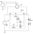
- FIG. 1 is an explanatory diagram illustrating a configuration example of an arc suppression device according to an embodiment of the present disclosure.
- FIG. 1 shows a configuration example of an arc suppression device for suppressing the generation of an arc when power is cut off.
- the arc suppression device shown in FIG. 1 includes a switch S1 configured by, for example, SSR (Solid State Relay), and a current limiting circuit AF1a.
- the switch S1 is configured to be switched on and off by electric power from the DC power supply V2.
- the switch S1 When the switch S1 is on, power from the power source V1 that supplies DC power is supplied to the resistor R4.
- the switch S1 When the switch S1 is off, the supply of power from the power source V1 to the resistor R4 is interrupted.
- the current limiting circuit AF1a includes a MOSFET (Metal-Oxide-Semiconductor Field-Effect Transistor) M1, a Zener diode D1, resistors R1 and R2, and a capacitor C1.
- MOSFET Metal-Oxide-Semiconductor Field-Effect Transistor
- D1 and R2 resistors R1 and R2
- capacitor C1 The current limiting circuit AF1a is a circuit that suppresses the occurrence of an arc in the switch S1 when the current is interrupted by the switch S1 while power is supplied from the power supply V1.
- MOSFET M1 an enhancement type NMOSFET is used as the MOSFET M1.
- the MOSFET M1 is provided on a path through which a current flows from the power supply V1.
- the capacitor C1 is provided between the drain terminal and the gate terminal of the MOSFET M1.
- the resistor R1 is provided between the gate terminal and the source terminal of the MOSFET M1.
- the resistor R1 is provided to set a time for applying a voltage to the gate terminal of the MOSFET M1 together with the capacitor C1.
- the capacitor C1 and the resistor R1 are connected in series.
- the zener diode D1 is provided to discharge the electric charge stored in the capacitor C1 when the contact of the switch S1 is connected.
- the Zener diode D1 is provided to protect the gate terminal of the MOSFET M1.
- a predetermined potential difference is generated between the terminals of the switch S1. This potential difference corresponds to the voltage value of the power supply V1 at the time of interruption.
- the potential difference generated between the terminals of the switch S1 induces the gate voltage of the MOSFET M1 through the capacitor C1, and turns on the MOSFET M1.
- a current flows in a direction that reduces the potential difference between the terminals of the switch S1. That is, when the MOSFET M1 is turned on, a current flows from the node N1 to the node N2. That is, when the terminals of the switch S1 are separated from each other, voltage integration is started by the voltage passing through the capacitor C1 and the current fixed by the resistor R1.
- the voltage between the drain terminal and the source terminal of the MOSFET M1 falls within the voltage along the transfer function of the FET gate voltage.
- the gate voltage of the MOSFET M1 decreases.
- the MOSFET M1 will eventually be turned off.
- the voltage integration in the current limiting circuit AF1a ends when the current stops flowing through the MOSFET M1.
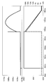
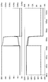
- FIG. 2 is a graph showing changes in the voltage at the node N2 of the current limiting circuit AF1a and the current flowing through the MOSFET M1 and the change in power consumption in the MOSFET M1 when power is supplied from the power source V1 and when power is cut off.
- FIG. The voltage at the node N2 of the current limiting circuit AF1a is indicated by a solid line in the lower graph of FIG. 2
- the change in the current flowing through the MOSFET M1 is indicated by a broken line in the lower graph of FIG. 2
- the change in power consumption in the MOSFET M1 is This is shown in the upper graph of FIG.
- description will be made assuming that 200 V DC power is supplied from the power source V1.
- the resistor R4 is 10 ⁇
- the inductor L1 is 0.01 mH
- the resistor R1 in the current limiting circuit AF1a is 20 k ⁇
- the resistor R2 is 20 ⁇
- the capacitor C1 is 0.04 ⁇ F.
- the switch S1 is turned on at 15 msec and the switch S1 is turned off at 95 msec.
- the voltage at the node N2 and the current flowing through the MOSFET M1 become zero at about 140 msec. That is, a current flows through the MOSFET M1 for about 45 msec.
- the change in power consumption in MOSFET M1 is shown in the upper graph of FIG. 2.
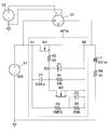
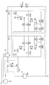
- FIG. 3 is an explanatory diagram illustrating a configuration example of the arc suppression device according to the embodiment of the present disclosure.
- FIG. 3 shows a configuration example of an arc suppression device for suppressing the generation of an arc when power is cut off.
- the arc suppression device shown in FIG. 3 includes a switch S1 configured by, for example, SSR, and a current limiting circuit AF1b.
- the switch S1 is configured to be switched on and off by electric power from the DC power supply V2.
- the switch S1 When the switch S1 is on, power from the power source V1 that supplies DC power is supplied to the resistor R4.
- the switch S1 When the switch S1 is off, the supply of power from the power source V1 to the resistor R4 is interrupted.
- the current limiting circuit AF1b includes MOSFETs M1 and M2, Zener diodes D1 and D3, resistors R1, R2, R3, and R5, and a capacitor C1.
- the current limiting circuit AF1b is a circuit that suppresses the occurrence of an arc in the switch S1 when the current is interrupted by the switch S1 while power is supplied from the power supply V1.
- the current limiting circuit AF1b shown in FIG. The MOSFET M2, which is an NMOSFET, a Zener diode D3, and resistors R3 and R5 are further added to the current limiting circuit AF1a shown in FIG.
- the resistors R3 and R5 divide the voltage generated between the nodes N1 and N2 when voltage integration by the current limiting circuit AF1b is started when the power supplied from the power source V1 is cut off by the switch S1.
- the MOSFET M2 is turned on when the gate-source voltage reaches a predetermined value. The fact that the MOSFET M2 is turned on means that the gate and the source of the MOSFET M1 are short-circuited. When the MOSFET M2 is turned on and the gate and the source of the MOSFET M1 are short-circuited, the MOSFET M1 is turned off, and the voltage integration by the current limiting circuit AF1b is completed.
- the Zener diode D3 is provided for protecting the MOSFET M2.
- FIG. 4 is a graph showing changes in the voltage of the node N2 of the current limiting circuit AF1b and the current flowing through the MOSFET M1 and the change in power consumption in the MOSFET M1 when power is supplied from the power source V1 and when power is cut off.
- FIG. The voltage of the node N2 of the current limiting circuit AF1b is indicated by a solid line in the lower graph of FIG. 4
- the change of the current flowing through the MOSFET M1 is indicated by the broken line in the lower graph of FIG. 4
- the change of the power consumption in the MOSFET M1 is This is shown in the upper graph of FIG.
- description will be made assuming that 200 V DC power is supplied from the power source V1.
- the resistor R4 is 10 ⁇
- the inductor L1 is 0.01 mH
- the resistor R1 in the current limiting circuit AF1b is 20 k ⁇
- the resistor R2 is 20 ⁇
- the resistor R3 is 1 M ⁇
- R5 is 200 k ⁇
- the capacitor C1 is 0.04 ⁇ F. Further, it is assumed that the MOSFET M2 is turned on when the gate-source voltage becomes 5V.
- the switch S1 is turned on at 15 msec and the switch S1 is turned off at 95 msec.
- the switch S1 when the DC power of 200V from the power source V1 is cut off by the switch S1, voltage integration by the voltage passing through the capacitor C1 and the current fixed by the resistor R1 starts.
- the voltage integration starts, the voltage generated between the nodes N1 and N2 is divided by the resistors R3 and R5, and the voltage across the resistor R5 reaches 5V, which is the voltage at which the MOSFET M2 is turned on.
- the MOSFET M2 is turned on.
- MOSFET M2 When MOSFET M2 is turned on, the gate and source of MOSFET M1 are short-circuited, and voltage integration is completed.
- the power consumption of the MOSFET M1 can be greatly reduced as compared with the current limiting circuit AF1a.
- the line after 95 msec indicated by a broken line is the upper graph of FIG. 2 for comparison when the MOSFET M2 does not operate (that is, when it is equivalent to the circuit of FIG. 1).
- the change in power consumption in the MOSFET M1 indicated by is superimposed and displayed.
- the line after 95 msec indicated by the alternate long and short dash line indicates the case where the MOSFET M2 does not operate (that is, the equivalent of the circuit of FIG.
- the change of the current flowing through the MOSFET M1 shown in the graph is superimposed and displayed.
- the current limiting circuit AF1b according to the second configuration example of the embodiment of the present disclosure can greatly reduce the power consumption of the MOSFET M1, and the voltage supplied from the power supply V1 is doubled. Even so, the power consumption of the MOSFET M1 is limited to twice, so that the current limiting circuit AF1b according to the second configuration example of the embodiment of the present disclosure can avoid an increase in the size of the MOSFET M1. .
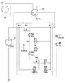
- FIG. 5 is an explanatory diagram illustrating a configuration example of the arc suppression device according to the embodiment of the present disclosure.
- FIG. 5 shows a configuration example of an arc suppression device for suppressing the generation of an arc when power is cut off.
- the arc suppression device shown in FIG. 5 includes a switch S1 configured by, for example, SSR, and a current limiting circuit AF1c.
- the switch S1 is configured to be switched on and off by electric power from the DC power supply V2.
- the switch S1 When the switch S1 is on, power from the power source V1 that supplies DC power is supplied to the resistor R4.
- the switch S1 When the switch S1 is off, the supply of power from the power source V1 to the resistor R4 is interrupted.
- the current limiting circuit AF1c includes MOSFETs M1 and M2, Zener diodes D1 and D3, resistors R1, R2, R3, R5, and R6, and a capacitor C1.
- the current limiting circuit AF1c is a circuit that suppresses the occurrence of an arc in the switch S1 when the current is interrupted by the switch S1 while power is supplied from the power supply V1.
- the current limiting circuit AF1c has a configuration in which a resistor R6 is added compared to the current limiting circuit AF1b.
- the resistor R6 is in parallel with the resistor R1 when the voltage at both ends of the resistor R5 reaches a voltage at which the MOSFET M2 is turned on when the DC power from the power source V1 is cut off by the switch S1, and the MOSFET M2 is turned on. It is provided to integrate at high speed by being connected to. That is, in the configuration of the arc suppression device shown in FIG. 3, when the MOSFET M2 is turned on, only the capacitor C1 exists between the power source V1 and the resistor R4 as a load. In the configuration of the arc suppression device shown in FIG.
- FIG. 6 is a graph showing changes in the voltage at the node N2 of the current limiting circuit AF1c, the current flowing through the MOSFET M1, and the change in power consumption in the MOSFET M1 when power is supplied from the power source V1 and when power is cut off.
- the voltage of the node N2 of the current limiting circuit AF1c is indicated by a solid line in the lower graph of FIG. 6, the change of the current flowing through the MOSFET M1 is indicated by a broken line in the lower graph of FIG. 6, and the change of the power consumption in the MOSFET M1 is This is shown in the upper graph of FIG.
- description will be made assuming that 200 V DC power is supplied from the power source V1.
- the resistor R4 is 10 ⁇
- the inductor L1 is 0.01 mH
- the resistor R1 in the current limiting circuit AF1b is 20 k ⁇
- the resistor R2 is 20 ⁇
- the resistor R3 is 1 M ⁇
- R5 is 200 k ⁇
- R6 is 50 ⁇
- the capacitor C1 is 0.04 ⁇ F.
- the MOSFET M2 is turned on when the gate-source voltage becomes 5V.
- the surge component (second peak power in FIG. 4) present in the solid line graph showing the change in power consumption in the MOSFET M1 in FIG. It can be seen that the current limiting circuit AF1c reduces the portion of FIG.
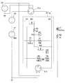
- FIG. 7 is an explanatory diagram illustrating a configuration example of the arc suppression device according to the embodiment of the present disclosure.
- FIG. 7 shows a configuration example of an arc suppression device for suppressing the generation of an arc when power is cut off.
- the arc suppression device shown in FIG. 7 includes, for example, a switch S1 configured by SSR, a current limiting circuit AF1d, a fuse F1, and a protector PF1.
- the switch S1 is configured to be switched on and off by electric power from the DC power supply V2.
- the switch S1 When the switch S1 is on, power from the power source V1 that supplies DC power is supplied to the resistor R4.
- the switch S1 When the switch S1 is off, the supply of power from the power source V1 to the resistor R4 is interrupted.
- the current limiting circuit AF1d has the same configuration as the current limiting circuit AF1c shown in FIG. That is, the current limiting circuit AF1d includes MOSFETs M1 and M2, Zener diodes D1 and D3, resistors R1, R2, R3, R5, and R6, and a capacitor C1.
- the current limiting circuit AF1d is a circuit that suppresses the occurrence of an arc in the switch S1 when the current is interrupted by the switch S1 while power is supplied from the power supply V1.
- the protector PF1 is provided to bypass the current flowing from the power supply V1 to the current limiting circuit AF1d when the MOSFET M1 fails (that is, when the MOSFET M1 does not function as a switching element and becomes a simple resistor) It consists of two fuses and a resistor R7 provided between the two fuses. That is, the protector PF1 has three terminals. The resistor R7 has a role of forcibly blowing the fuse inside the protector PF1. As shown in FIG. 7, the fuse F1 is provided between the power source V1 and the current limiting circuit AF1d.
- the arc suppression device shown in FIG. 7 can safely cut off the power when the MOSFET M1 fails (when it does not function as a switch) by providing the fuse F1 and the protector PF1. It becomes.
- FIG. 8 is an explanatory diagram illustrating a configuration example of the arc suppression device according to the embodiment of the present disclosure.
- FIG. 8 shows a configuration example of an arc suppression device for suppressing the generation of an arc when power is cut off.
- the arc suppression device shown in FIG. 8 includes, for example, a switch S1 configured by SSR, current limiting circuits AF1e and AF2e, a fuse F1, and a protector PF1.
- the switch S1 is configured to be switched on and off by electric power from the DC power supply V2.
- the switch S1 When the switch S1 is on, power from the power source V1 that supplies power is supplied to the resistor R4.
- the switch S1 When the switch S1 is off, the supply of power from the power source V1 to the resistor R4 is interrupted.
- the current limiting circuit AF1e includes MOSFETs M1 and M2, Zener diodes D1 and D3, a diode D5, resistors R1, R2, R3, R5, and R6, and a capacitor C1.
- the current limiting circuit AF1e is a circuit that suppresses the occurrence of an arc in the switch S1 when the current is interrupted by the switch S1 while power is supplied from the node N1 side.
- the current limiting circuit AF2e has a configuration obtained by inverting the current limiting circuit AF1e. That is, the current limiting circuit AF2e includes MOSFETs M3 and M4, Zener diodes D2 and D4, a diode D6, resistors R8, R9, R10, R11, and R12, and a capacitor C2.
- the current limiting circuit AF2e is a circuit that suppresses the occurrence of an arc in the switch S1 when the current is cut off by the switch S1 while power is supplied from the node N3 side.
- the current limiting circuit AF1e has a function of gradually decreasing the current flowing from the node N1 to the node N3 when the switch S1 is turned off while the current is flowing from the node N1 to the node N3. Therefore, the diode D6 is provided in the current limiting circuit AF2e, and a current flows from the node N1 to the node N3 side.
- the current limiting circuit AF2e has a function of gradually decreasing the current flowing from the node N3 to the node N1 when the switch S1 is turned off while the current flows from the node N3 to the node N1. Therefore, the diode D5 is provided in the current limiting circuit AF1e, and a current flows from the node N3 to the node N1 side.
- the arc suppression device shown in FIG. 8 can suppress an arc when power is cut off while preventing an increase in circuit scale even when power is supplied bidirectionally instead of unidirectionally.
- the arc suppression device shown in FIG. 8 is provided with a fuse F1 and a protector PF1 similarly to the arc suppression device shown in FIG. 7, but the arc suppression device shown in FIG. 8 includes a fuse F1 and a protector. PF1 may not be provided.
- FIG. 9 is an explanatory diagram illustrating a configuration example of the arc suppression device according to the embodiment of the present disclosure.
- FIG. 9 shows a configuration example of an arc suppression device for suppressing the generation of an arc when power is cut off.
- the arc suppression device shown in FIG. 9 includes, for example, a switch S1 configured by SSR, current limiting circuits AF1f and AF2f, a fuse F1, and a protector PF1.
- the switch S1 is configured to be switched on and off by electric power from the DC power supply V2.
- the switch S1 When the switch S1 is on, power from the power source V1 that supplies power is supplied to the resistor R4.
- the switch S1 When the switch S1 is off, the supply of power from the power source V1 to the resistor R4 is interrupted.
- the current limiting circuit AF1f includes MOSFETs M1 and M2, Zener diodes D1 and D3, a diode D5, resistors R1, R2, R3, R5, and R6, and a capacitor C1.
- the current limiting circuit AF1f is a circuit that suppresses the occurrence of an arc in the switch S1 when the current is cut off by the switch S1 while power is supplied from the node N1 side.
- the current limiting circuit AF2f has a configuration in which the current limiting circuit AF1e is inverted. That is, the current limiting circuit AF2f includes MOSFETs M3 and M4, Zener diodes D2 and D4, a diode D6, resistors R8, R9, R10, R11, and R12, and a capacitor C2.
- the current limiting circuit AF2e is a circuit that suppresses the occurrence of an arc in the switch S1 when the current is cut off by the switch S1 while power is supplied from the node N3 side.
- the current limiting circuit AF1f has a function of gradually decreasing the current flowing from the node N1 to the node N3 when the switch S1 is turned off while the current flows from the node N1 to the node N3. Therefore, the current limiting circuit AF1f is provided with a diode D5, and a current flows from the node N1 to the node N3. Further, the current limiting circuit AF2f is provided with a diode D6, which cuts off the current flowing from the node N1 to the node N3.
- the current limiting circuit AF2f has a function of gradually reducing the current flowing from the node N3 to the node N1 when the switch S1 is turned off while the current flows from the node N3 to the node N1. Therefore, a diode D6 is provided in the current limiting circuit AF2f, and a current flows from the node N3 to the node N1 side. In addition, the current limiting circuit AF1f is provided with a diode D5, which cuts off the current flowing from the node N3 to the node N1.
- the arc suppression device shown in FIG. 9 can suppress an arc when power is cut off while preventing an increase in circuit scale even when power is supplied bidirectionally instead of unidirectionally.
- the arc suppression device shown in FIG. 9 is provided with a fuse F1 and a protector PF1 similarly to the arc suppression device shown in FIG. 7, but the arc suppression device shown in FIG. 9 has a fuse F1 and a protector. PF1 may not be provided.
- FIG. 10 is an explanatory diagram illustrating a configuration example of the arc suppression device according to the embodiment of the present disclosure.
- FIG. 10 shows a configuration example of an arc suppression device for suppressing the generation of an arc when power is cut off.
- the arc suppression device shown in FIG. 10 includes switches S1a and S1b configured by, for example, SSR, and a current limiting circuit AF1g.
- FIG. 10 shows a configuration example of the arc suppression device when the power supplied from the power source V1 or the power source V3 is cut off.
- the power source V1 is a power source that supplies DC power
- the power source V3 is a power source that supplies AC power.
- the switch S1a is configured to be switched on and off by electric power from the DC power supply V2.
- the switch S1a When the switch S1a is on, power from the power supply V1 or V3 that supplies power is supplied to the resistor R4.
- the switch S1a When the switch S1a is off, the supply of power from the power source V1 or V3 to the resistor R4 is cut off.
- the switch S1b operates in conjunction with the switch S1a, and is turned off when the switch S1a is on and turned on when the switch S1a is off.
- the switches S1a and S1b are illustrated apart from each other, but are equivalent to a transfer type contact having a make break contact with the node N2 as a common.
- the current limiting circuit AF1g includes MOSFETs M1 and M2, Zener diodes D1 and D3, resistors R1, R3, R4, and R5, and a capacitor C1.
- the current limiting circuit AF1f is a circuit that suppresses the occurrence of an arc in the switch S1a when the current is cut off by the switch S1 while power is supplied from the node N1 side.
- the switch S1a When the switch S1a is turned off, the voltage generated between the nodes N1 and N2 is divided by the resistors R4 and R5.
- the MOSFET M2 is turned on when the gate-source voltage reaches a predetermined value.
- the fact that the MOSFET M2 is turned on means that the gate and the source of the MOSFET M1 are short-circuited.
- the MOSFET M1 When the MOSFET M2 is turned on and the gate and the source of the MOSFET M1 are short-circuited, the MOSFET M1 is turned off, and the voltage integration by the current limiting circuit AF1b is completed.
- the switch S1b when the switch S1b is off, the gate and the source of the MOSFET M1 are not short-circuited. However, when the switch S1b is on, the gate and the source of the MOSFET M1 are short-circuited. . When the gate and source of the MOSFET M1 are short-circuited, as described in the second configuration example, the MOSFET M1 is turned off, and the voltage integration by the current limiting circuit AF1g is completed.
- the switch S1b is turned on and the gate and the source of the MOSFET M1 are short-circuited before the MOSFET M2 is turned on by voltage division by the resistors R4 and R5, the current limiting circuit AF1g is switched to the switch S1b.
- the short circuit between the gate and the source of the MOSFET M1 is prioritized.
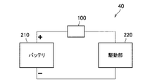
- FIG. 11 is an explanatory diagram illustrating a functional configuration example of the moving body 40 including the arc suppression device.
- the moving body 40 may be, for example, a moving body that uses gasoline as a power source, such as a gasoline car, and uses a chargeable / dischargeable battery as a main power source, such as an electric vehicle, a hybrid vehicle, and an electric motorcycle. It may be a body.
- the moving body 40 includes a battery 210, a drive unit 220 that is driven by electric power supplied from the battery, and an arc suppression device 100 that suppresses an arc when the electric power from the battery 210 is interrupted.
- the drive unit 220 may include, for example, equipment provided in the vehicle such as a wiper, a power window, a light, a car navigation system, and an air conditioner, and a device that drives the moving body 40 such as a motor.
- the arc suppression device 100 is provided in the middle of a path in which DC power is supplied from the battery 210 to the drive unit 220.
- the arc suppression device 100 for example, the arc suppression devices shown in FIGS. 1, 3, 5, and 7 to 10 may be used.
- the moving body 40 shown in FIG. 11 can safely block DC current by providing the arc suppression device 100 on a path through which DC power is supplied from the battery 210 to the drive unit 220.
- FIG. 11 shows an example of the moving body 40 provided with only one arc suppression device 100, but the present disclosure is not limited to such an example.
- a plurality of arc suppression devices 100 may be provided in the middle of a route through which DC power is supplied.
- the arc suppression device 100 may be provided not only in the middle of a path in which DC power is supplied from the battery 210 to the drive unit 220 but also in another place, for example, in the middle of a path when charging the battery 210 with DC power. good.
- the moving body 40 can safely charge the battery 210 with DC power by providing the arc suppression device 100 in the middle of the path when charging the battery 210 with DC power.
- an arc suppression device and an arc suppression device capable of reducing the power consumption at the time of power interruption by reducing the size of a mechanical contact used for power interruption.
- a power supply system including a moving body provided with the arc suppression device.
- At least one current limiting circuit provided in parallel with a circuit breaker that switches between supply and interruption of power from the power source, The current limiting circuit cuts off the current from the power source when the power from the power source is supplied to the load via a breaker, When the supply of power from the power source to the load is interrupted by the circuit breaker, the current from the power source when the voltage generated by the potential difference between the contacts of the circuit breaker generated at the time of the circuit breakage exceeds a predetermined voltage
- An arc suppression device that shuts off (2) The current limiting circuit is: When power from the power source is supplied to the load via the circuit breaker, the power is turned off, and when power from the power source to the load is interrupted by the circuit breaker, the power is interrupted.
- a first switching element that is turned on after a current caused by the difference is turned on after being turned on due to a potential difference between the contacts of the circuit breaker;
- the arc suppression device according to (1) comprising: (3)
- the said current limiting circuit is an arc suppression apparatus as described in said (2) provided with the capacitive element which raises the gate voltage of a said 1st switching element, when supply to the said load of the electric power from the said power supply is interrupted
- the said current limiting circuit is an arc suppression apparatus as described in said (3) provided with the resistive element which sets the time which applies a voltage to the gate terminal of a said 1st switching element with the said capacitive element.
- the current limiting circuit further includes a switch that is turned on when supply of power from the power source to the load is interrupted, and short-circuits between the gate terminal and the source terminal of the first switching element, The arc suppression device according to any one of (2) to (5).
- the arc suppression device according to any one of (1) to (6), wherein the power supplied from the power source is DC power.
- At least one current limiting circuit provided in parallel with a circuit breaker that switches between supply and interruption of power from the power source,
- the current limiting circuit is: When the power from the power source is supplied to the load via the circuit breaker, the power is turned off, and when the AC power from the power source is interrupted by the circuit breaker, the power is interrupted A first switching element that is turned on after the current generated by the potential difference is turned on after being turned on by the potential difference between the contacts of the circuit breaker; A capacitive element that increases the gate voltage of the first switching element when the supply of power from the power source to the load is interrupted; A second switching element that is turned on in response to the potential difference and short-circuits between the gate terminal and the source terminal of the first switching element;
- An arc suppression device comprising: (9)
- the said current limiting circuit is an arc suppression apparatus as described in said (8) provided with the resistive element which sets the time which applies a voltage to the gate terminal of a said 1st switching element with the said capacitive element.
- the arc limiting device includes a Zener diode between a source terminal and a gate terminal of the first switching element.
- the current limiting circuit further includes a switch that is turned on when supply of power from the power source to the load is interrupted, and short-circuits between the gate terminal and the source terminal of the first switching element, (8) The arc suppression device according to any one of (10).
- a moving body comprising one or more arc suppression devices according to any one of (1) to (12).
- a power supply system comprising:
- arc suppression device 210 battery 220: driving unit AF1a, AF1b, AF1c, AF1d, AF1e, AF1f, AF1g, AF2e, AF2f: current limiting circuit
- F1 fuse PF1: protectors S1, S1a, S1b: switch
- V1 Power supply
- V2 DC power supply
Landscapes
- Engineering & Computer Science (AREA)
- Power Engineering (AREA)
- Mechanical Engineering (AREA)
- Emergency Protection Circuit Devices (AREA)
- Driving Mechanisms And Operating Circuits Of Arc-Extinguishing High-Tension Switches (AREA)
- Relay Circuits (AREA)
- Dc-Dc Converters (AREA)
Abstract
【課題】電力の遮断時に発生するアーク抑制に用いられる電流制限回路の消費電力を低減して、電力の遮断時の半導体における電力消費を低減させることが可能な、新規かつ改良されたアーク抑制装置を提供する。 【解決手段】電源からの電力の供給と遮断とを切り替える遮断器と並列に設けられる電流制限回路を少なくとも一つ備え、前記電流制限回路は、前記電源からの電力が遮断機を介して負荷に供給される際には前記電源からの電流を遮断し、前記電源からの電力の前記負荷への供給が前記遮断機により遮断される際には遮断時に発生する前記遮断機の接点間の電位差により生じる電圧が所定電圧以上になったとき前記電源からの電流を遮断する、アーク抑制装置が提供される。
Description
本開示は、アーク抑制装置、移動体及び電力供給システムに関する。
直流給電でも交流給電でも、電力の切断時にはアーク放電が発生する。交流の場合、所定の時間毎(例えば10ミリ秒毎)に電圧がゼロとなる瞬間があるので、アーク放電は少なくとも上記所定の時間内(例えば10ミリ秒以内)に自然に止まる。しかし直流給電では、ゼロ電圧となる瞬間がないため、アーク放電は自然には止まらない。
そのため、直流給電の場合に電力の切断時にアーク放電の発生を抑えることを目的とした技術が開示されている(特許文献1,2等参照)。
遮断しようとする電力が大きくなればなるほど、電力の遮断時に発生するアークの抑制に用いられる電流制限回路の大型化が避けられず、また遮断にも時間を要することになり、遮断の開始から終了までに電流制限回路で消費する電力が増えてしまう。
そこで、本開示では、電力の遮断時に発生するアークの抑制に用いられる電流制限回路の消費電力を低減して、電力の遮断時の半導体における電力消費を低減させることが可能な、新規かつ改良されたアーク抑制装置、移動体及び電力供給システムを提案する。
本開示によれば、電源からの電力の供給と遮断とを切り替える遮断器と並列に設けられる電流制限回路を少なくとも一つ備え、前記電流制限回路は、前記電源からの電力が遮断機を介して負荷に供給される際には前記電源からの電流を遮断し、前記電源からの電力の前記負荷への供給が前記遮断機により遮断される際には遮断時に発生する前記遮断機の接点間の電位差により生じる電圧が所定電圧以上になったとき前記電源からの電流を遮断する、アーク抑制装置が提供される。
また本開示によれば、電源からの電力の供給と遮断とを切り替える遮断器と並列に設けられる電流制限回路を少なくとも一つ備え、前記電流制限回路は、前記電源からの電力が遮断機を介して負荷に供給される際にはオフ状態となり、前記電源からの交流電力の前記負荷への供給が前記遮断機により遮断される際には遮断時に発生する前記遮断機の接点間の電位差によりオン状態となった後、該電位差により生じる電流を流した後にオフ状態となる第1スイッチング素子と、前記電源からの電力の前記負荷への供給が遮断された際に前記第1スイッチング素子のゲート電圧を上昇させる容量素子と、前記電位差に応じてオン状態となり前記第1スイッチング素子のゲート端子とソース端子との間を短絡させる第2スイッチング素子と、を備える、アーク抑制装置が提供される。
また本開示によれば、1以上の上記アーク抑制装置を備える、移動体が提供される。
また本開示によれば、直流電力を供給するバッテリと、前記バッテリから供給される直流電力による駆動する駆動部と、前記バッテリと前記駆動部との間に設けられる、少なくとも1つの、請求項1に記載のアーク抑制装置と、を備える、電力供給システムが提供される。
以上説明したように本開示によれば、電力の遮断時に発生するアークの抑制に用いられる電流制限回路の消費電力を低減して、電力の遮断時の半導体における電力消費を低減させることが可能な、新規かつ改良されたアーク抑制装置、移動体及び電力供給システムを提供することが出来る。
なお、上記の効果は必ずしも限定的なものではなく、上記の効果とともに、または上記の効果に代えて、本明細書に示されたいずれかの効果、または本明細書から把握され得る他の効果が奏されてもよい。
以下に添付図面を参照しながら、本開示の好適な実施の形態について詳細に説明する。なお、本明細書及び図面において、実質的に同一の機能構成を有する構成要素については、同一の符号を付することにより重複説明を省略する。
なお、説明は以下の順序で行うものとする。
1.本開示の実施の形態
1.1.第1の構成例
1.2.第2の構成例
1.3.第3の構成例
1.4.第4の構成例
1.5.第5の構成例
1.6.第6の構成例
1.7.第7の構成例
2.応用例
3.まとめ
1.本開示の実施の形態
1.1.第1の構成例
1.2.第2の構成例
1.3.第3の構成例
1.4.第4の構成例
1.5.第5の構成例
1.6.第6の構成例
1.7.第7の構成例
2.応用例
3.まとめ
<1.本開示の実施の形態>
[1.1.第1の構成例]
まず、図1を参照して、本開示の実施の形態の第1の構成例を説明する。図1は、本開示の実施の形態に係るアーク抑制装置の構成例を示す説明図である。図1に示したのは、電力の遮断時にアークの発生を抑制させるためのアーク抑制装置の構成例である。図1に示したアーク抑制装置は、例えばSSR(Solid State Relay)で構成されるスイッチS1と、電流制限回路AF1aと、を含んで構成される。
[1.1.第1の構成例]
まず、図1を参照して、本開示の実施の形態の第1の構成例を説明する。図1は、本開示の実施の形態に係るアーク抑制装置の構成例を示す説明図である。図1に示したのは、電力の遮断時にアークの発生を抑制させるためのアーク抑制装置の構成例である。図1に示したアーク抑制装置は、例えばSSR(Solid State Relay)で構成されるスイッチS1と、電流制限回路AF1aと、を含んで構成される。
スイッチS1は、直流電源V2からの電力によりオンとオフとが切り替わるよう構成される。スイッチS1がオンの場合には、直流の電力を供給する電源V1からの電力が抵抗R4に供給される。スイッチS1がオフの場合には、電源V1からの電力の抵抗R4への供給が遮断される。
電流制限回路AF1aは、MOSFET(Metal-Oxide-Semiconductor Field-Effect Transistor) M1と、ツェナーダイオードD1と、抵抗R1、R2と、コンデンサC1と、を有する。電流制限回路AF1aは、電源V1から電力が供給されている状態でスイッチS1により電流の遮断がなされた際に、スイッチS1でのアークの発生を抑制する回路である。
電流制限回路AF1aを構成する各素子について説明する。MOSFET M1は、本実施形態ではエンハンスメント型のNMOSFETを用いている。MOSFET M1は電源V1から電流が流れる経路上に設けられる。コンデンサC1は、MOSFET M1のドレイン端子とゲート端子との間に設けられる。また抵抗R1は、MOSFET M1のゲート端子とソース端子との間に設けられる。抵抗R1は、MOSFET M1のゲート端子に電圧を印加する時間を、コンデンサC1と共に設定するために設けられる。そしてコンデンサC1と抵抗R1とは直列に接続されている。ツェナーダイオードD1は、スイッチS1の接点が接続された際に、コンデンサC1に蓄えられている電荷を放電するために設けられる。またツェナーダイオードD1は、MOSFET M1のゲート端子の保護のために設けられる。
続いて電流制限回路AF1aの機能について説明する。スイッチS1がオン状態にある際は、MOSFET M1はオフ状態となっている。従って電流制限回路AF1aには電流が流れない。
スイッチS1により電流の遮断がなされると、スイッチS1の端子間に所定の電位差が発生する。この電位差は、遮断時の電源V1の電圧値に対応する。スイッチS1の端子間に発生した電位差は、コンデンサC1を介してMOSFET M1のゲート電圧を誘起させて、MOSFET M1をオン状態にする。MOSFET M1がオン状態となると、スイッチS1の端子間の電位差を低下させる方向に電流が流れる。すなわちMOSFET M1がオン状態となると、ノードN1からノードN2の方向に電流が流れる。すなわち、スイッチS1の端子間が乖離すると、コンデンサC1を通した電圧と、抵抗R1で固定された電流による電圧積分が始まる。
MOSFET M1がオン状態となると、スイッチS1の端子間の電位差を低下させる方向に電流が流れることにより、スイッチS1の端子間の電位差が低減される。従って、電源V1から電力が供給されている状態でスイッチS1により電流の遮断がなされた際に、仮にアークの発生条件を満たしていた場合であっても、スイッチS1においてアークの発生に至ることは無い。
MOSFET M1のドレイン端子とソース端子との間の電圧は、FETのゲート電圧による伝達関数に沿った電圧に収まる。スイッチS1の端子間に発生した電位差によってコンデンサC1の充電が進むと、MOSFET M1のゲート電圧が低下する。MOSFET M1のゲート電圧が低下するとやがてMOSFET M1はオフ状態に移行する。MOSFET M1がオフ状態に移行することでMOSFET M1に電流が流れなくなる。MOSFET M1に電流が流れなくなったことで電流制限回路AF1aにおける電圧積分が終了する。
図2は、電源V1からの電力の供給時及び電力の遮断時における、電流制限回路AF1aのノードN2の電圧及びMOSFET M1を流れる電流の変化、並びにMOSFET M1における消費電力の変化をグラフで示す説明図である。電流制限回路AF1aのノードN2の電圧は図2の下のグラフにおいて実線で示され、MOSFET M1を流れる電流の変化は図2の下のグラフにおいて破線で示され、MOSFET M1における消費電力の変化は図2の上のグラフにおいて示されている。ここでは、電源V1から200Vの直流電力が供給されているとして説明する。抵抗R4は10Ω、インダクタL1は0.01mH、電流制限回路AF1aにおける抵抗R1は20kΩ、抵抗R2は20Ω、コンデンサC1は0.04μFであるとする。
図2に示した例では、15msecの時点でスイッチS1がオンし、95msecの時点でスイッチS1がオフする。この場合、図2に示したように、電源V1からの200Vの直流電力をスイッチS1で遮断する際には、およそ140msecの時点で、ノードN2の電圧及びMOSFET M1を流れる電流が0となる。すなわち、およそ45msecの間、MOSFET M1に電流が流れる。図2の上側のグラフにMOSFET M1における消費電力の変化が示されているが、95msecからおよそ140msecの間の45msecの範囲において、上に凸の曲線と時間軸で囲まれる範囲を積分することにより、MOSFET M1での発熱量が求められる。すなわち、この例では、電源V1からの200Vの直流電力をスイッチS1で遮断する際には、MOSFET M1でおよそ40Jの発熱量が発生する。
[1.2.第2の構成例]
第1の構成例のように、スイッチS1と並列に電流制限回路AF1aを備えることで、スイッチS1での電力の遮断時にアークの発生を抑えることができる。一方、遮断しようとする電力の電圧が上昇すると、その上昇に伴ってMOSFET M1に掛かる電圧やMOSFET M1に流れる電流が0になるまでの時間も長くなる。図2に示したように、MOSFET M1に掛かる電圧やMOSFET M1に流れる電流は、時間と共に比例して低下する。従って、MOSFET M1に掛かる電圧が2倍になると、MOSFET M1に掛かる電圧やMOSFET M1に流れる電流が0になるまでの時間が2倍になり、MOSFET M1での発熱量は4倍になる。
第1の構成例のように、スイッチS1と並列に電流制限回路AF1aを備えることで、スイッチS1での電力の遮断時にアークの発生を抑えることができる。一方、遮断しようとする電力の電圧が上昇すると、その上昇に伴ってMOSFET M1に掛かる電圧やMOSFET M1に流れる電流が0になるまでの時間も長くなる。図2に示したように、MOSFET M1に掛かる電圧やMOSFET M1に流れる電流は、時間と共に比例して低下する。従って、MOSFET M1に掛かる電圧が2倍になると、MOSFET M1に掛かる電圧やMOSFET M1に流れる電流が0になるまでの時間が2倍になり、MOSFET M1での発熱量は4倍になる。
そこで、第2の構成例では、電流制限回路に掛かる電圧が所定量降下すると、電流制限回路における電圧積分を終了させるようにした構成を説明する。
図3は、本開示の実施の形態に係るアーク抑制装置の構成例を示す説明図である。図3に示したのは、電力の遮断時にアークの発生を抑制させるためのアーク抑制装置の構成例である。図3に示したアーク抑制装置は、例えばSSRで構成されるスイッチS1と、電流制限回路AF1bと、を含んで構成される。
スイッチS1は、直流電源V2からの電力によりオンとオフとが切り替わるよう構成される。スイッチS1がオンの場合には、直流の電力を供給する電源V1からの電力が抵抗R4に供給される。スイッチS1がオフの場合には、電源V1からの電力の抵抗R4への供給が遮断される。
電流制限回路AF1bは、MOSFET M1、M2と、ツェナーダイオードD1、D3と、抵抗R1、R2、R3、R5と、コンデンサC1と、を有する。電流制限回路AF1bは、電源V1から電力が供給されている状態でスイッチS1により電流の遮断がなされた際に、スイッチS1でのアークの発生を抑制する回路である。
図3に示した電流制限回路AF1bは.図1に示した電流制限回路AF1aから、さらにNMOSFETであるMOSFET M2と、ツェナーダイオードD3と、抵抗R3、R5と、が追加されたものである。
抵抗R3、R5は、電源V1から供給される電力をスイッチS1で遮断する際に、電流制限回路AF1bによる電圧積分が開始されると、ノードN1とN2との間に発生する電圧を分圧する。MOSFET M2は、ゲート-ソース間の電圧が所定の値になるとオン状態となる。MOSFET M2がオン状態になるということは、MOSFET M1のゲートとソースとの間がショートされることを意味する。MOSFET M2がオン状態になり、MOSFET M1のゲートとソースとの間がショートされると、MOSFET M1がオフ状態になり、電流制限回路AF1bによる電圧積分が終了する。またツェナーダイオードD3は、MOSFET M2の保護のために設けられている。
図4は、電源V1からの電力の供給時及び電力の遮断時における、電流制限回路AF1bのノードN2の電圧及びMOSFET M1を流れる電流の変化、並びにMOSFET M1における消費電力の変化をグラフで示す説明図である。電流制限回路AF1bのノードN2の電圧は図4の下のグラフにおいて実線で示され、MOSFET M1を流れる電流の変化は図4の下のグラフにおいて破線で示され、MOSFET M1における消費電力の変化は図4の上のグラフにおいて示されている。ここでは、電源V1から200Vの直流電力が供給されているとして説明する。抵抗R4は10Ω、インダクタL1は0.01mH、電流制限回路AF1bにおける抵抗R1は20kΩ、抵抗R2は20Ω、抵抗R3は1MΩ、R5は200kΩ、コンデンサC1は0.04μFであるとする。また、MOSFET M2は、ゲート-ソース間の電圧が5Vになるとオン状態になるとする。
図4に示した例では、15msecの時点でスイッチS1がオンし、95msecの時点でスイッチS1がオフする。この場合、図4に示したように、電源V1からの200Vの直流電力をスイッチS1で遮断する際には、コンデンサC1を通した電圧と、抵抗R1で固定された電流による電圧積分が始まる。電圧積分が始まると、ノードN1とN2との間に発生する電圧が、抵抗R3、R5により分圧され、抵抗R5の両端の電圧が、MOSFET M2がオン状態に変化する電圧である5Vに達すると、MOSFET M2がオン状態になる。MOSFET M2がオン状態になると、MOSFET M1のゲートとソースとの間がショートされ、電圧積分が終了する。
95msecの時点でスイッチS1が遮断されたのち、電流制限回路AF1bによる電圧積分が行われている期間、MOSFET M1に電流が流れる。図4の上側のグラフにMOSFET M1における消費電力の変化が示されるが、95msec以降の非常に短い期間において、2つのピークを含み上に凸の実線と時間軸で囲まれる範囲を積分することにより、MOSFET M1での発熱量が求められる。すなわち、電流制限回路AF1bのMOSFET M1による電力消費は、およそ2Jとなる。このように、MOSFET M2と、MOSFET M2をオン状態にさせる抵抗R3、R5を設けることで、電流制限回路AF1aと比べて大きくMOSFET M1の消費電力量を低下させることが出来る。なお、図4の上のグラフにおいて、破線で示す95msec以後のラインは、MOSFET M2が動作しない場合(すなわち図1の回路と等価である場合)について、比較のために、図2の上のグラフで示されるMOSFET M1における消費電力の変化を重ねて表示したものである。また、図4の下のグラフにおいて、一点鎖線で示す95msec以後のラインは、MOSFET M2が動作しない場合(すなわち図1の回路と等価である場合)について、比較のために、図2の下のグラフで示されるMOSFET M1を流れる電流の変化を重ねて表示したものである。
従って、本開示の実施の形態の第2の構成例に係る電流制限回路AF1bは、MOSFET M1の消費電力量を大きく低下させることができ、また、電源V1から供給される電圧が2倍になったとしても、MOSFET M1の消費電力量は2倍が限度となるので、本開示の実施の形態の第2の構成例に係る電流制限回路AF1bは、MOSFET M1の大型化を回避することができる。
[1.3.第3の構成例]
第2の構成例のように電流制限回路を構成することで、MOSFET M1の消費電力量を大きく低下させることが可能になる。次に、負荷にコイル成分が含まれている際に生じうるサージを抑制する構成を追加したアーク抑制装置の例を説明する。
第2の構成例のように電流制限回路を構成することで、MOSFET M1の消費電力量を大きく低下させることが可能になる。次に、負荷にコイル成分が含まれている際に生じうるサージを抑制する構成を追加したアーク抑制装置の例を説明する。
図5は、本開示の実施の形態に係るアーク抑制装置の構成例を示す説明図である。図5に示したのは、電力の遮断時にアークの発生を抑制させるためのアーク抑制装置の構成例である。図5に示したアーク抑制装置は、例えばSSRで構成されるスイッチS1と、電流制限回路AF1cと、を含んで構成される。
スイッチS1は、直流電源V2からの電力によりオンとオフとが切り替わるよう構成される。スイッチS1がオンの場合には、直流の電力を供給する電源V1からの電力が抵抗R4に供給される。スイッチS1がオフの場合には、電源V1からの電力の抵抗R4への供給が遮断される。
電流制限回路AF1cは、MOSFET M1、M2と、ツェナーダイオードD1、D3と、抵抗R1、R2、R3、R5、R6と、コンデンサC1と、を有する。電流制限回路AF1cは、電源V1から電力が供給されている状態でスイッチS1により電流の遮断がなされた際に、スイッチS1でのアークの発生を抑制する回路である。
電流制限回路AF1cは、電流制限回路AF1bに比べると、抵抗R6が追加された構成を有する。抵抗R6は、電源V1からの直流電力をスイッチS1で遮断する際に、抵抗R5の両端の電圧がMOSFET M2がオン状態に変化する電圧に達してMOSFET M2がオン状態になると、抵抗R1と並列に接続されることで高速に積分を行うように設けられている。すなわち、図3に示したアーク抑制装置の構成では、MOSFET M2がオン状態に変化すると、電源V1と負荷である抵抗R4との間にはコンデンサC1のみが存在する構成であったが、図3に示したアーク抑制装置の構成では、MOSFET M2がオン状態に変化すると、電源V1と負荷である抵抗R4との間にはコンデンサC1と抵抗R6とが存在する構成となっている。電源V1と負荷である抵抗R4との間にはコンデンサC1と抵抗R6とが存在する構成となっていることで、電流制限回路AF1cは、MOSFET M2がオン状態に変化しても、漏れ電流を低減させることが可能となる。
図6は、電源V1からの電力の供給時及び電力の遮断時における、電流制限回路AF1cのノードN2の電圧及びMOSFET M1を流れる電流の変化、並びにMOSFET M1における消費電力の変化をグラフで示す説明図である。電流制限回路AF1cのノードN2の電圧は図6の下のグラフにおいて実線で示され、MOSFET M1を流れる電流の変化は図6の下のグラフにおいて破線で示され、MOSFET M1における消費電力の変化は図6の上のグラフにおいて示されている。ここでは、電源V1から200Vの直流電力が供給されているとして説明する。抵抗R4は10Ω、インダクタL1は0.01mH、電流制限回路AF1bにおける抵抗R1は20kΩ、抵抗R2は20Ω、抵抗R3は1MΩ、R5は200kΩ、R6は50Ω、コンデンサC1は0.04μFであるとする。また、MOSFET M2は、ゲート-ソース間の電圧が5Vになるとオン状態になるとする。
図6に示したように、抵抗R6が設けられていることで、図4のMOSFET M1における消費電力の変化を示した実線グラフにおいて存在していたサージ成分(図4における2つ目のピーク電力の部分)を、電流制限回路AF1cでは低減させていることが分かる。
[1.4.第4の構成例]
第3の構成例のように電流制限回路を構成することで、MOSFET M1の消費電力量を大きく低下させるとともに、遮断時に発生しうるサージ成分を抑制することが可能になる。次に、MOSFET M1が故障した場合(スイッチとして機能しなくなった場合)に安全に電力を遮断できる構成を追加したアーク抑制装置の例を説明する。
第3の構成例のように電流制限回路を構成することで、MOSFET M1の消費電力量を大きく低下させるとともに、遮断時に発生しうるサージ成分を抑制することが可能になる。次に、MOSFET M1が故障した場合(スイッチとして機能しなくなった場合)に安全に電力を遮断できる構成を追加したアーク抑制装置の例を説明する。
図7は、本開示の実施の形態に係るアーク抑制装置の構成例を示す説明図である。図7に示したのは、電力の遮断時にアークの発生を抑制させるためのアーク抑制装置の構成例である。図7に示したアーク抑制装置は、例えばSSRで構成されるスイッチS1と、電流制限回路AF1dと、ヒューズF1と、プロテクタPF1と、を含んで構成される。
スイッチS1は、直流電源V2からの電力によりオンとオフとが切り替わるよう構成される。スイッチS1がオンの場合には、直流の電力を供給する電源V1からの電力が抵抗R4に供給される。スイッチS1がオフの場合には、電源V1からの電力の抵抗R4への供給が遮断される。
電流制限回路AF1dは、図5に示した電流制限回路AF1cと同様の構成を有する。すなわち電流制限回路AF1dは、MOSFET M1、M2と、ツェナーダイオードD1、D3と、抵抗R1、R2、R3、R5、R6と、コンデンサC1と、を有する。電流制限回路AF1dは、電源V1から電力が供給されている状態でスイッチS1により電流の遮断がなされた際に、スイッチS1でのアークの発生を抑制する回路である。
プロテクタPF1は、MOSFET M1の故障時(つまりMOSFET M1がスイッチング素子として機能せず、単なる抵抗となった場合)に、電源V1から電流制限回路AF1dに流れる電流を迂回させるために設けられており、2つのヒューズと、該2つのヒューズの間に設けられる抵抗R7と、からなる。すなわち、プロテクタPF1は3つの端子を有している。抵抗R7は、プロテクタPF1の内部のヒューズを強制的に溶断させる役割を有する。ヒューズF1は、図7に示したように電源V1と電流制限回路AF1dとの間に設けられる。
従って、図7に示したアーク抑制装置は、ヒューズF1と、プロテクタPF1とが設けられることで、MOSFET M1が故障した場合(スイッチとして機能しなくなった場合)に安全に電力を遮断させることが可能となる。
[1.5.第5の構成例]
第4の構成例のように、MOSFET M1が故障した場合であっても、安全に電力を遮断することができる。次に、一方向では無く双方向に電力が供給される場合にも、回路規模の増大を防ぎつつ電力の遮断時にアークを抑制できるアーク抑制装置の例を説明する。
第4の構成例のように、MOSFET M1が故障した場合であっても、安全に電力を遮断することができる。次に、一方向では無く双方向に電力が供給される場合にも、回路規模の増大を防ぎつつ電力の遮断時にアークを抑制できるアーク抑制装置の例を説明する。
図8は、本開示の実施の形態に係るアーク抑制装置の構成例を示す説明図である。図8に示したのは、電力の遮断時にアークの発生を抑制させるためのアーク抑制装置の構成例である。図8に示したアーク抑制装置は、例えばSSRで構成されるスイッチS1と、電流制限回路AF1e、AF2eと、ヒューズF1と、プロテクタPF1と、を含んで構成される。
スイッチS1は、直流電源V2からの電力によりオンとオフとが切り替わるよう構成される。スイッチS1がオンの場合には、電力を供給する電源V1からの電力が抵抗R4に供給される。スイッチS1がオフの場合には、電源V1からの電力の抵抗R4への供給が遮断される。
電流制限回路AF1eは、MOSFET M1、M2と、ツェナーダイオードD1、D3と、ダイオードD5と、抵抗R1、R2、R3、R5、R6と、コンデンサC1と、を有する。電流制限回路AF1eは、ノードN1の側から電力が供給されている状態でスイッチS1により電流の遮断がなされた際に、スイッチS1でのアークの発生を抑制する回路である。
電流制限回路AF2eは、電流制限回路AF1eを反転させた構成を有する。すなわち電流制限回路AF2eは、MOSFET M3、M4と、ツェナーダイオードD2、D4と、ダイオードD6と、抵抗R8、R9、R10、R11、R12と、コンデンサC2と、を有する。電流制限回路AF2eは、ノードN3の側から電力が供給されている状態でスイッチS1により電流の遮断がなされた際に、スイッチS1でのアークの発生を抑制する回路である。
電流制限回路AF1eは、ノードN1からノードN3の側に電流が流れている際にスイッチS1がオフになると、ノードN1からノードN3の側に流れる電流を徐々に低下させる機能を有する。そのため、電流制限回路AF2eにはダイオードD6が設けられており、ノードN1からノードN3の側に電流を流している。
一方、電流制限回路AF2eは、ノードN3からノードN1の側に電流が流れている際にスイッチS1がオフになると、ノードN3からノードN1の側に流れる電流を徐々に低下させる機能を有する。そのため、電流制限回路AF1eにはダイオードD5が設けられており、ノードN3からノードN1の側に電流を流している。
図8に示したアーク抑制装置は、一方向では無く双方向に電力が供給される場合にも、回路規模の増大を防ぎつつ電力の遮断時にアークを抑制できる。図8に示したアーク抑制装置には、図7に示したアーク抑制装置と同様にヒューズF1と、プロテクタPF1とが設けられているが、図8に示したアーク抑制装置にヒューズF1と、プロテクタPF1とが設けられていなくても良い。
[1.6.第6の構成例]
第5の構成例のように、一方向では無く双方向に電力が供給される場合にも、回路規模の増大を防ぎつつ電力の遮断時にアークを抑制できる。第5の構成例では、電流制限回路は直列に接続されていたが、電流制限回路は並列に接続されていても良い。
第5の構成例のように、一方向では無く双方向に電力が供給される場合にも、回路規模の増大を防ぎつつ電力の遮断時にアークを抑制できる。第5の構成例では、電流制限回路は直列に接続されていたが、電流制限回路は並列に接続されていても良い。
図9は、本開示の実施の形態に係るアーク抑制装置の構成例を示す説明図である。図9に示したのは、電力の遮断時にアークの発生を抑制させるためのアーク抑制装置の構成例である。図9に示したアーク抑制装置は、例えばSSRで構成されるスイッチS1と、電流制限回路AF1f、AF2fと、ヒューズF1と、プロテクタPF1と、を含んで構成される。
スイッチS1は、直流電源V2からの電力によりオンとオフとが切り替わるよう構成される。スイッチS1がオンの場合には、電力を供給する電源V1からの電力が抵抗R4に供給される。スイッチS1がオフの場合には、電源V1からの電力の抵抗R4への供給が遮断される。
電流制限回路AF1fは、MOSFET M1、M2と、ツェナーダイオードD1、D3と、ダイオードD5と、抵抗R1、R2、R3、R5、R6と、コンデンサC1と、を有する。電流制限回路AF1fは、ノードN1の側から電力が供給されている状態でスイッチS1により電流の遮断がなされた際に、スイッチS1でのアークの発生を抑制する回路である。
電流制限回路AF2fは、電流制限回路AF1eを反転させた構成を有する。すなわち電流制限回路AF2fは、MOSFET M3、M4と、ツェナーダイオードD2、D4と、ダイオードD6と、抵抗R8、R9、R10、R11、R12と、コンデンサC2と、を有する。電流制限回路AF2eは、ノードN3の側から電力が供給されている状態でスイッチS1により電流の遮断がなされた際に、スイッチS1でのアークの発生を抑制する回路である。
電流制限回路AF1fは、ノードN1からノードN3の側に電流が流れている際にスイッチS1がオフになると、ノードN1からノードN3の側に流れる電流を徐々に低下させる機能を有する。そのため、電流制限回路AF1fにはダイオードD5が設けられており、ノードN1からノードN3の側に電流を流す。また、電流制限回路AF2fにはダイオードD6が設けられており、ノードN1からノードN3の側に流れる電流を遮断している。
一方、電流制限回路AF2fは、ノードN3からノードN1の側に電流が流れている際にスイッチS1がオフになると、ノードN3からノードN1の側に流れる電流を徐々に低下させる機能を有する。そのため、電流制限回路AF2fにはダイオードD6が設けられており、ノードN3からノードN1の側に電流を流す。また、電流制限回路AF1fにはダイオードD5が設けられており、ノードN3からノードN1に流れる電流を遮断している。
図9に示したアーク抑制装置は、一方向では無く双方向に電力が供給される場合にも、回路規模の増大を防ぎつつ電力の遮断時にアークを抑制できる。図9に示したアーク抑制装置には、図7に示したアーク抑制装置と同様にヒューズF1と、プロテクタPF1とが設けられているが、図9に示したアーク抑制装置にヒューズF1と、プロテクタPF1とが設けられていなくても良い。
[1.7.第7の構成例]
図10は、本開示の実施の形態に係るアーク抑制装置の構成例を示す説明図である。図10に示したのは、電力の遮断時にアークの発生を抑制させるためのアーク抑制装置の構成例である。図10に示したアーク抑制装置は、例えばSSRで構成されるスイッチS1a、S1bと、電流制限回路AF1gと、を含んで構成される。図10には、電源V1または電源V3から供給される電力を遮断する際のアーク抑制装置の構成例が示されている。電源V1は直流電力を供給する電源であり、電源V3は交流電力を供給する電源である。
図10は、本開示の実施の形態に係るアーク抑制装置の構成例を示す説明図である。図10に示したのは、電力の遮断時にアークの発生を抑制させるためのアーク抑制装置の構成例である。図10に示したアーク抑制装置は、例えばSSRで構成されるスイッチS1a、S1bと、電流制限回路AF1gと、を含んで構成される。図10には、電源V1または電源V3から供給される電力を遮断する際のアーク抑制装置の構成例が示されている。電源V1は直流電力を供給する電源であり、電源V3は交流電力を供給する電源である。
スイッチS1aは、直流電源V2からの電力によりオンとオフとが切り替わるよう構成される。スイッチS1aがオンの場合には、電力を供給する電源V1または電源V3からの電力が抵抗R4に供給される。スイッチS1aがオフの場合には、電源V1または電源V3からの電力の抵抗R4への供給が遮断される。
スイッチS1bは、スイッチS1aと連動して動作し、スイッチS1aがオンの場合にはオフに、オフの場合にはオンになるスイッチである。図10では、スイッチS1aとS1bとは離れて図示されているが、ノードN2をコモンとしたメークブレーク接点を持つトランスファー型接点と同等である。
電流制限回路AF1gは、MOSFET M1、M2と、ツェナーダイオードD1、D3と、抵抗R1、R3、R4、R5と、コンデンサC1と、を有する。電流制限回路AF1fは、ノードN1の側から電力が供給されている状態でスイッチS1により電流の遮断がなされた際に、スイッチS1aでのアークの発生を抑制する回路である。
スイッチS1aがオフになると、ノードN1とN2との間に発生する電圧を抵抗R4、R5で分圧する。MOSFET M2は、ゲート-ソース間の電圧が所定の値になるとオン状態となる。MOSFET M2がオン状態になるということは、MOSFET M1のゲートとソースとの間がショートされることを意味する。MOSFET M2がオン状態になり、MOSFET M1のゲートとソースとの間がショートされると、MOSFET M1がオフ状態になり、電流制限回路AF1bによる電圧積分が終了する。
ここで、スイッチS1bがオフ状態の場合は、MOSFET M1のゲートとソースとの間はショートされていないが、スイッチS1bがオン状態になると、MOSFET M1のゲートとソースとの間がショート状態になる。MOSFET M1のゲートとソースとの間がショート状態になると、第2の構成例で説明したように、MOSFET M1がオフ状態になり、電流制限回路AF1gによる電圧積分が終了する。
電流制限回路AF1gは、抵抗R4、R5による分圧によってMOSFET M2がオンになるより前に、スイッチS1bがオン状態になってMOSFET M1のゲートとソースとの間がショート状態となれば、スイッチS1bによるMOSFET M1のゲートとソースとの間のショートを優先させる構成としている。
<2.応用例>
図11は、アーク抑制装置を備えた移動体40の機能構成例を示す説明図である。移動体40は、例えば、ガソリン車のようにガソリンを動力源とする移動体であってもよく、電気自動車、ハイブリッド車、電気オートバイ等の、充放電可能なバッテリを主な動力源とする移動体であってもよい。図11には、移動体40に、バッテリ210と、バッテリから供給される電力により駆動する駆動部220と、バッテリ210からの電力の遮断時にアークを抑制するアーク抑制装置100と、が備えられた場合の例が示されている。駆動部220には、例えばワイパー、パワーウィンドウ、ライト、カーナビゲーションシステム、エアーコンディショナのような車両に備えられる装備品や、モーター等の移動体40を駆動させる装置などが含まれうる。
図11は、アーク抑制装置を備えた移動体40の機能構成例を示す説明図である。移動体40は、例えば、ガソリン車のようにガソリンを動力源とする移動体であってもよく、電気自動車、ハイブリッド車、電気オートバイ等の、充放電可能なバッテリを主な動力源とする移動体であってもよい。図11には、移動体40に、バッテリ210と、バッテリから供給される電力により駆動する駆動部220と、バッテリ210からの電力の遮断時にアークを抑制するアーク抑制装置100と、が備えられた場合の例が示されている。駆動部220には、例えばワイパー、パワーウィンドウ、ライト、カーナビゲーションシステム、エアーコンディショナのような車両に備えられる装備品や、モーター等の移動体40を駆動させる装置などが含まれうる。
そして図11に示した移動体40には、バッテリ210から駆動部220へ直流電力が供給される経路の途中に、アーク抑制装置100が設けられている。アーク抑制装置100は、例えば上記の図1、図3、図5、図7~10に示したアーク抑制装置が用いられ得る。図11に示した移動体40は、バッテリ210から駆動部220へ直流電力が供給される経路上に、アーク抑制装置100が設けられることで、安全に直流電流を遮断することができる。
なお図11には、アーク抑制装置100が1つだけ備えられている移動体40の例を示したが、本開示は係る例に限定されるものではない。すなわち、アーク抑制装置100は直流電力が供給される経路の途中に複数設けられても良い。またアーク抑制装置100は、バッテリ210から駆動部220へ直流電力が供給される経路の途中だけでなく、他の場所、例えばバッテリ210を直流電力で充電する際の経路の途中に設けられても良い。移動体40は、バッテリ210を直流電力で充電する際の経路の途中にアーク抑制装置100を設けることで、安全にバッテリ210を直流電力で充電することができる。
<3.まとめ>
以上説明したように本開示の実施の形態によれば、電力の遮断に用いられる機械接点を小型化して、電力の遮断時の電力消費を低減させることが可能なアーク抑制装置、アーク抑制装置を備えた移動体、及びアーク抑制装置を備えた電力供給システムが提供される。
以上説明したように本開示の実施の形態によれば、電力の遮断に用いられる機械接点を小型化して、電力の遮断時の電力消費を低減させることが可能なアーク抑制装置、アーク抑制装置を備えた移動体、及びアーク抑制装置を備えた電力供給システムが提供される。
以上、添付図面を参照しながら本開示の好適な実施形態について詳細に説明したが、本開示の技術的範囲はかかる例に限定されない。本開示の技術分野における通常の知識を有する者であれば、特許請求の範囲に記載された技術的思想の範疇内において、各種の変更例または修正例に想到し得ることは明らかであり、これらについても、当然に本開示の技術的範囲に属するものと了解される。
また、本明細書に記載された効果は、あくまで説明的または例示的なものであって限定的ではない。つまり、本開示に係る技術は、上記の効果とともに、または上記の効果に代えて、本明細書の記載から当業者には明らかな他の効果を奏しうる。
なお、以下のような構成も本開示の技術的範囲に属する。
(1)
電源からの電力の供給と遮断とを切り替える遮断器と並列に設けられる電流制限回路を少なくとも一つ備え、
前記電流制限回路は、前記電源からの電力が遮断機を介して負荷に供給される際には前記電源からの電流を遮断し、
前記電源からの電力の前記負荷への供給が前記遮断機により遮断される際には遮断時に発生する前記遮断機の接点間の電位差により生じる電圧が所定電圧以上になったとき前記電源からの電流を遮断する、アーク抑制装置。
(2)
前記電流制限回路は、
前記電源からの電力が前記遮断機を介して前記負荷に供給される際にはオフ状態となり、前記電源からの電力の前記負荷への供給が前記遮断機により遮断される際には遮断時に発生する前記遮断機の接点間の電位差によりオン状態となった後、該差により生じる電流を流した後にオフ状態となる第1スイッチング素子と、
前記電位差に応じてオン状態となり前記第1スイッチング素子のゲート端子とソース端子との間を短絡させる第2スイッチング素子と、
を備える、前記(1)に記載のアーク抑制装置。
(3)
前記電流制限回路は、前記電源からの電力の前記負荷への供給が遮断された際に前記第1スイッチング素子のゲート電圧を上昇させる容量素子を備える、前記(2)に記載のアーク抑制装置。
(4)
前記電流制限回路は、前記第1スイッチング素子のゲート端子に電圧を印加する時間を、前記容量素子と共に設定する抵抗素子を備える、前記(3)に記載のアーク抑制装置。
(5)
前記電流制限回路は、前記第1スイッチング素子のソース端子とゲート端子との間にツェナーダイオードを備える、前記(3)に記載のアーク抑制装置。
(6)
前記電流制限回路は、さらに、前記電源からの電力の前記負荷への供給が遮断される際にオン状態となり前記第1スイッチング素子のゲート端子とソース端子との間を短絡させるスイッチを備える、前記(2)~(5)のいずれかに記載のアーク抑制装置。
(7)
前記電源から供給される電力は、直流電力である、前記(1)~(6)のいずれかに記載のアーク抑制装置。
(8)
電源からの電力の供給と遮断とを切り替える遮断器と並列に設けられる電流制限回路を少なくとも一つ備え、
前記電流制限回路は、
前記電源からの電力が遮断機を介して負荷に供給される際にはオフ状態となり、前記電源からの交流電力の前記負荷への供給が前記遮断機により遮断される際には遮断時に発生する前記遮断機の接点間の電位差によりオン状態となった後、該電位差により生じる電流を流した後にオフ状態となる第1スイッチング素子と、
前記電源からの電力の前記負荷への供給が遮断される際に前記第1スイッチング素子のゲート電圧を上昇させる容量素子と、
前記電位差に応じてオン状態となり前記第1スイッチング素子のゲート端子とソース端子との間を短絡させる第2スイッチング素子と、
を備える、アーク抑制装置。
(9)
前記電流制限回路は、前記第1スイッチング素子のゲート端子に電圧を印加する時間を、前記容量素子と共に設定する抵抗素子を備える、前記(8)に記載のアーク抑制装置。
(10)
前記電流制限回路は、前記第1スイッチング素子のソース端子とゲート端子との間にツェナーダイオードを備える、前記(8)または(9)に記載のアーク抑制装置。
(11)
前記電流制限回路は、さらに、前記電源からの電力の前記負荷への供給が遮断される際にオン状態となり前記第1スイッチング素子のゲート端子とソース端子との間を短絡させるスイッチを備える、前記(8)~(10)のいずれかに記載のアーク抑制装置。
(12)
前記電源から供給される電力は、直流電力である、前記(8)~(11)に記載のアーク抑制装置。
(13)
1以上の前記(1)~(12)のいずれかに記載のアーク抑制装置を備える、移動体。
(14)
直流電力を供給するバッテリと、
前記バッテリから供給される直流電力による駆動する駆動部と、
前記バッテリと前記駆動部との間に設けられる、少なくとも1つの、前記(1)~(12)のいずれかに記載のアーク抑制装置と、
を備える、電力供給システム。
(1)
電源からの電力の供給と遮断とを切り替える遮断器と並列に設けられる電流制限回路を少なくとも一つ備え、
前記電流制限回路は、前記電源からの電力が遮断機を介して負荷に供給される際には前記電源からの電流を遮断し、
前記電源からの電力の前記負荷への供給が前記遮断機により遮断される際には遮断時に発生する前記遮断機の接点間の電位差により生じる電圧が所定電圧以上になったとき前記電源からの電流を遮断する、アーク抑制装置。
(2)
前記電流制限回路は、
前記電源からの電力が前記遮断機を介して前記負荷に供給される際にはオフ状態となり、前記電源からの電力の前記負荷への供給が前記遮断機により遮断される際には遮断時に発生する前記遮断機の接点間の電位差によりオン状態となった後、該差により生じる電流を流した後にオフ状態となる第1スイッチング素子と、
前記電位差に応じてオン状態となり前記第1スイッチング素子のゲート端子とソース端子との間を短絡させる第2スイッチング素子と、
を備える、前記(1)に記載のアーク抑制装置。
(3)
前記電流制限回路は、前記電源からの電力の前記負荷への供給が遮断された際に前記第1スイッチング素子のゲート電圧を上昇させる容量素子を備える、前記(2)に記載のアーク抑制装置。
(4)
前記電流制限回路は、前記第1スイッチング素子のゲート端子に電圧を印加する時間を、前記容量素子と共に設定する抵抗素子を備える、前記(3)に記載のアーク抑制装置。
(5)
前記電流制限回路は、前記第1スイッチング素子のソース端子とゲート端子との間にツェナーダイオードを備える、前記(3)に記載のアーク抑制装置。
(6)
前記電流制限回路は、さらに、前記電源からの電力の前記負荷への供給が遮断される際にオン状態となり前記第1スイッチング素子のゲート端子とソース端子との間を短絡させるスイッチを備える、前記(2)~(5)のいずれかに記載のアーク抑制装置。
(7)
前記電源から供給される電力は、直流電力である、前記(1)~(6)のいずれかに記載のアーク抑制装置。
(8)
電源からの電力の供給と遮断とを切り替える遮断器と並列に設けられる電流制限回路を少なくとも一つ備え、
前記電流制限回路は、
前記電源からの電力が遮断機を介して負荷に供給される際にはオフ状態となり、前記電源からの交流電力の前記負荷への供給が前記遮断機により遮断される際には遮断時に発生する前記遮断機の接点間の電位差によりオン状態となった後、該電位差により生じる電流を流した後にオフ状態となる第1スイッチング素子と、
前記電源からの電力の前記負荷への供給が遮断される際に前記第1スイッチング素子のゲート電圧を上昇させる容量素子と、
前記電位差に応じてオン状態となり前記第1スイッチング素子のゲート端子とソース端子との間を短絡させる第2スイッチング素子と、
を備える、アーク抑制装置。
(9)
前記電流制限回路は、前記第1スイッチング素子のゲート端子に電圧を印加する時間を、前記容量素子と共に設定する抵抗素子を備える、前記(8)に記載のアーク抑制装置。
(10)
前記電流制限回路は、前記第1スイッチング素子のソース端子とゲート端子との間にツェナーダイオードを備える、前記(8)または(9)に記載のアーク抑制装置。
(11)
前記電流制限回路は、さらに、前記電源からの電力の前記負荷への供給が遮断される際にオン状態となり前記第1スイッチング素子のゲート端子とソース端子との間を短絡させるスイッチを備える、前記(8)~(10)のいずれかに記載のアーク抑制装置。
(12)
前記電源から供給される電力は、直流電力である、前記(8)~(11)に記載のアーク抑制装置。
(13)
1以上の前記(1)~(12)のいずれかに記載のアーク抑制装置を備える、移動体。
(14)
直流電力を供給するバッテリと、
前記バッテリから供給される直流電力による駆動する駆動部と、
前記バッテリと前記駆動部との間に設けられる、少なくとも1つの、前記(1)~(12)のいずれかに記載のアーク抑制装置と、
を備える、電力供給システム。
40 :移動体
100 :アーク抑制装置
210 :バッテリ
220 :駆動部
AF1a、AF1b、AF1c、AF1d、AF1e、AF1f、AF1g、AF2e、AF2f :電流制限回路
F1 :ヒューズ
PF1 :プロテクタ
S1、S1a、S1b :スイッチ
V1 :電源
V2 :直流電源
100 :アーク抑制装置
210 :バッテリ
220 :駆動部
AF1a、AF1b、AF1c、AF1d、AF1e、AF1f、AF1g、AF2e、AF2f :電流制限回路
F1 :ヒューズ
PF1 :プロテクタ
S1、S1a、S1b :スイッチ
V1 :電源
V2 :直流電源
Claims (14)
- 電源からの電力の供給と遮断とを切り替える遮断器と並列に設けられる電流制限回路を少なくとも一つ備え、
前記電流制限回路は、前記電源からの電力が遮断機を介して負荷に供給される際には前記電源からの電流を遮断し、
前記電源からの電力の前記負荷への供給が前記遮断機により遮断される際には遮断時に発生する前記遮断機の接点間の電位差により生じる電圧が所定電圧以上になったとき前記電源からの電流を遮断する、アーク抑制装置。 - 前記電流制限回路は、
前記電源からの電力が前記遮断機を介して前記負荷に供給される際にはオフ状態となり、前記電源からの電力の前記負荷への供給が前記遮断機により遮断される際には遮断時に発生する前記遮断機の接点間の電位差によりオン状態となった後、該差により生じる電流を流した後にオフ状態となる第1スイッチング素子と、
前記電位差に応じてオン状態となり前記第1スイッチング素子のゲート端子とソース端子との間を短絡させる第2スイッチング素子と、
を備える、請求項1に記載のアーク抑制装置。 - 前記電流制限回路は、前記電源からの電力の前記負荷への供給が遮断された際に前記第1スイッチング素子のゲート電圧を上昇させる容量素子を備える、請求項2に記載のアーク抑制装置。
- 前記電流制限回路は、前記第1スイッチング素子のゲート端子に電圧を印加する時間を、前記容量素子と共に設定する抵抗素子を備える、請求項3に記載のアーク抑制装置。
- 前記電流制限回路は、前記第1スイッチング素子のソース端子とゲート端子との間にツェナーダイオードを備える、請求項3に記載のアーク抑制装置。
- 前記電流制限回路は、さらに、前記電源からの電力の前記負荷への供給が遮断される際にオン状態となり前記第1スイッチング素子のゲート端子とソース端子との間を短絡させるスイッチを備える、請求項2に記載のアーク抑制装置。
- 前記電源から供給される電力は、直流電力である、請求項1に記載のアーク抑制装置。
- 電源からの電力の供給と遮断とを切り替える遮断器と並列に設けられる電流制限回路を少なくとも一つ備え、
前記電流制限回路は、
前記電源からの電力が遮断機を介して負荷に供給される際にはオフ状態となり、前記電源からの交流電力の前記負荷への供給が前記遮断機により遮断される際には遮断時に発生する前記遮断機の接点間の電位差によりオン状態となった後、該電位差により生じる電流を流した後にオフ状態となる第1スイッチング素子と、
前記電源からの電力の前記負荷への供給が遮断される際に前記第1スイッチング素子のゲート電圧を上昇させる容量素子と、
前記電位差に応じてオン状態となり前記第1スイッチング素子のゲート端子とソース端子との間を短絡させる第2スイッチング素子と、
を備える、アーク抑制装置。 - 前記電流制限回路は、前記第1スイッチング素子のゲート端子に電圧を印加する時間を、前記容量素子と共に設定する抵抗素子を備える、請求項8に記載のアーク抑制装置。
- 前記電流制限回路は、前記第1スイッチング素子のソース端子とゲート端子との間にツェナーダイオードを備える、請求項8に記載のアーク抑制装置。
- 前記電流制限回路は、さらに、前記電源からの電力の前記負荷への供給が遮断される際にオン状態となり前記第1スイッチング素子のゲート端子とソース端子との間を短絡させるスイッチを備える、請求項8に記載のアーク抑制装置。
- 前記電源から供給される電力は、直流電力である、請求項8に記載のアーク抑制装置。
- 1以上の請求項1に記載のアーク抑制装置を備える、移動体。
- 直流電力を供給するバッテリと、
前記バッテリから供給される直流電力による駆動する駆動部と、
前記バッテリと前記駆動部との間に設けられる、少なくとも1つの、請求項1に記載のアーク抑制装置と、
を備える、電力供給システム。
Priority Applications (3)
| Application Number | Priority Date | Filing Date | Title |
|---|---|---|---|
| US16/493,474 US11189438B2 (en) | 2017-04-26 | 2018-03-06 | Arc suppression device, mobile body, and power supply system |
| JP2019515131A JP7226307B2 (ja) | 2017-04-26 | 2018-03-06 | アーク抑制装置、移動体及び電力供給システム |
| EP18792043.4A EP3618091A4 (en) | 2017-04-26 | 2018-03-06 | ARC SUPPRESSION DEVICE, MOVABLE BODY AND POWER SUPPLY SYSTEM |
Applications Claiming Priority (2)
| Application Number | Priority Date | Filing Date | Title |
|---|---|---|---|
| JP2017-087542 | 2017-04-26 | ||
| JP2017087542 | 2017-04-26 |
Publications (1)
| Publication Number | Publication Date |
|---|---|
| WO2018198538A1 true WO2018198538A1 (ja) | 2018-11-01 |
Family
ID=63920259
Family Applications (1)
| Application Number | Title | Priority Date | Filing Date |
|---|---|---|---|
| PCT/JP2018/008627 Ceased WO2018198538A1 (ja) | 2017-04-26 | 2018-03-06 | アーク抑制装置、移動体及び電力供給システム |
Country Status (4)
| Country | Link |
|---|---|
| US (1) | US11189438B2 (ja) |
| EP (1) | EP3618091A4 (ja) |
| JP (1) | JP7226307B2 (ja) |
| WO (1) | WO2018198538A1 (ja) |
Cited By (2)
| Publication number | Priority date | Publication date | Assignee | Title |
|---|---|---|---|---|
| JP2022519252A (ja) * | 2019-01-29 | 2022-03-22 | アーク サプレッション テクノロジーズ | 多相ac電源接点アーク抑制装置 |
| JP2024131436A (ja) * | 2023-03-16 | 2024-09-30 | Anp株式会社 | 直流開閉器 |
Families Citing this family (2)
| Publication number | Priority date | Publication date | Assignee | Title |
|---|---|---|---|---|
| CN115132519A (zh) * | 2021-03-26 | 2022-09-30 | 深圳市格瑞普电池有限公司 | 应急电源继电器灭弧控制系统及方法 |
| US12586738B2 (en) * | 2021-04-01 | 2026-03-24 | Hydra-Electric Company | Electronic snubber for elimination of switch contact impedance increase and arc contaminant deposition |
Citations (5)
| Publication number | Priority date | Publication date | Assignee | Title |
|---|---|---|---|---|
| JP2003203721A (ja) | 2002-01-08 | 2003-07-18 | Nippon Telegr & Teleph Corp <Ntt> | 直流コンセント |
| WO2011034140A1 (ja) * | 2009-09-16 | 2011-03-24 | 株式会社ワイ・ワイ・エル | スイッチ |
| JP2014522088A (ja) | 2011-08-10 | 2014-08-28 | エレンベルガー ウント ペンスケン ゲゼルシャフト ミット ベシュレンクテル ハフツング | メカトロニックな差込み接続システム |
| WO2016194584A1 (ja) * | 2015-06-04 | 2016-12-08 | ソニー株式会社 | 直流回路、直流電力供給装置、移動体及び電力供給システム |
| JP2017527067A (ja) * | 2014-06-18 | 2017-09-14 | エレンベルガー ウント ペンスケン ゲゼルシャフト ミット ベシュレンクテル ハフツング | 直流遮断用遮断スイッチ |
Family Cites Families (9)
| Publication number | Priority date | Publication date | Assignee | Title |
|---|---|---|---|---|
| US3912941A (en) * | 1974-04-15 | 1975-10-14 | Thomas M Passarella | Isolation circuit for arc reduction in a dc circuit |
| GB8402629D0 (en) * | 1984-02-01 | 1984-03-07 | Mcewan P M | Circuit breakers |
| US4658320A (en) * | 1985-03-08 | 1987-04-14 | Elecspec Corporation | Switch contact arc suppressor |
| US5703743A (en) | 1996-04-29 | 1997-12-30 | Schweitzer Engineering Laboratories, Inc. | Two terminal active arc suppressor |
| TWI249287B (en) | 2003-06-25 | 2006-02-11 | Matsushita Electric Works Ltd | Electronic switch |
| FR2977738B1 (fr) * | 2011-07-04 | 2015-01-16 | Mersen France Sb Sas | Systeme d'interruption de courant continu apte a ouvrir une ligne de courant continu a comportement inductif |
| EP2624274B1 (en) * | 2012-02-03 | 2014-12-31 | ABB S.p.A. | Hybrid current switching device |
| US20140091808A1 (en) * | 2012-09-28 | 2014-04-03 | Arc Suppression Technologies | Contact separation detector and methods therefor |
| WO2017018147A1 (ja) * | 2015-07-29 | 2017-02-02 | ソニー株式会社 | スイッチング装置、電動移動体及び電力供給システム |
-
2018
- 2018-03-06 US US16/493,474 patent/US11189438B2/en active Active
- 2018-03-06 JP JP2019515131A patent/JP7226307B2/ja active Active
- 2018-03-06 WO PCT/JP2018/008627 patent/WO2018198538A1/ja not_active Ceased
- 2018-03-06 EP EP18792043.4A patent/EP3618091A4/en not_active Withdrawn
Patent Citations (5)
| Publication number | Priority date | Publication date | Assignee | Title |
|---|---|---|---|---|
| JP2003203721A (ja) | 2002-01-08 | 2003-07-18 | Nippon Telegr & Teleph Corp <Ntt> | 直流コンセント |
| WO2011034140A1 (ja) * | 2009-09-16 | 2011-03-24 | 株式会社ワイ・ワイ・エル | スイッチ |
| JP2014522088A (ja) | 2011-08-10 | 2014-08-28 | エレンベルガー ウント ペンスケン ゲゼルシャフト ミット ベシュレンクテル ハフツング | メカトロニックな差込み接続システム |
| JP2017527067A (ja) * | 2014-06-18 | 2017-09-14 | エレンベルガー ウント ペンスケン ゲゼルシャフト ミット ベシュレンクテル ハフツング | 直流遮断用遮断スイッチ |
| WO2016194584A1 (ja) * | 2015-06-04 | 2016-12-08 | ソニー株式会社 | 直流回路、直流電力供給装置、移動体及び電力供給システム |
Non-Patent Citations (1)
| Title |
|---|
| See also references of EP3618091A4 |
Cited By (5)
| Publication number | Priority date | Publication date | Assignee | Title |
|---|---|---|---|---|
| JP2022519252A (ja) * | 2019-01-29 | 2022-03-22 | アーク サプレッション テクノロジーズ | 多相ac電源接点アーク抑制装置 |
| JP7111407B2 (ja) | 2019-01-29 | 2022-08-02 | アーク サプレッション テクノロジーズ | 多相ac電源接点アーク抑制装置 |
| US11798750B2 (en) | 2019-01-29 | 2023-10-24 | Arc Suppression Technologies | High power, multi-phase, AC power contact arc suppressor |
| JP2024131436A (ja) * | 2023-03-16 | 2024-09-30 | Anp株式会社 | 直流開閉器 |
| JP7714175B2 (ja) | 2023-03-16 | 2025-07-29 | Anp株式会社 | 直流開閉器 |
Also Published As
| Publication number | Publication date |
|---|---|
| JPWO2018198538A1 (ja) | 2020-05-21 |
| US20200135414A1 (en) | 2020-04-30 |
| EP3618091A1 (en) | 2020-03-04 |
| JP7226307B2 (ja) | 2023-02-21 |
| EP3618091A4 (en) | 2020-04-29 |
| US11189438B2 (en) | 2021-11-30 |
Similar Documents
| Publication | Publication Date | Title |
|---|---|---|
| JP6641862B2 (ja) | 電流制限回路、直流電力供給コネクタ及び直流電源装置 | |
| JP6623937B2 (ja) | リレー装置及び電源装置 | |
| KR102035033B1 (ko) | 전기 자동차용 파워 릴레이 어셈블리 및 파워 릴레이 어셈블리가 구비된 전기자동차용 에너지 시스템의 작동 방법 | |
| WO2018198538A1 (ja) | アーク抑制装置、移動体及び電力供給システム | |
| CN105270295A (zh) | 用于机动车辆的车载电气系统 | |
| WO2016194584A1 (ja) | 直流回路、直流電力供給装置、移動体及び電力供給システム | |
| JP7036033B2 (ja) | アーク抑制装置 | |
| WO2017018147A1 (ja) | スイッチング装置、電動移動体及び電力供給システム | |
| JP6011707B1 (ja) | スイッチング装置 | |
| CN109891543B (zh) | 直流开关装置的电弧消除装置 | |
| JP4508159B2 (ja) | エンジン始動装置 | |
| JP6977721B2 (ja) | 直流回路 | |
| JP7010245B2 (ja) | アーク抑制装置 | |
| JP7616482B2 (ja) | 車載用遮断電流供給装置 | |
| JP2019088085A (ja) | 電源システム | |
| KR101702039B1 (ko) | 포터블 배터리 충전기 | |
| KR20120018870A (ko) | 자동 복귀형 누전차단기의 액튜에이터 구동을 위한 급속 충전 회로 | |
| WO2018131250A1 (ja) | 直流開閉器のアーク消去装置 |
Legal Events
| Date | Code | Title | Description |
|---|---|---|---|
| 121 | Ep: the epo has been informed by wipo that ep was designated in this application |
Ref document number: 18792043 Country of ref document: EP Kind code of ref document: A1 |
|
| ENP | Entry into the national phase |
Ref document number: 2019515131 Country of ref document: JP Kind code of ref document: A |
|
| NENP | Non-entry into the national phase |
Ref country code: DE |
|
| ENP | Entry into the national phase |
Ref document number: 2018792043 Country of ref document: EP Effective date: 20191126 |