WO2018212041A1 - 量子ビットデバイス - Google Patents
量子ビットデバイス Download PDFInfo
- Publication number
- WO2018212041A1 WO2018212041A1 PCT/JP2018/017962 JP2018017962W WO2018212041A1 WO 2018212041 A1 WO2018212041 A1 WO 2018212041A1 JP 2018017962 W JP2018017962 W JP 2018017962W WO 2018212041 A1 WO2018212041 A1 WO 2018212041A1
- Authority
- WO
- WIPO (PCT)
- Prior art keywords
- superconducting
- qubit
- substrate
- wiring
- loop
- Prior art date
- Legal status (The legal status is an assumption and is not a legal conclusion. Google has not performed a legal analysis and makes no representation as to the accuracy of the status listed.)
- Ceased
Links
Images





Classifications
-
- H—ELECTRICITY
- H10—SEMICONDUCTOR DEVICES; ELECTRIC SOLID-STATE DEVICES NOT OTHERWISE PROVIDED FOR
- H10N—ELECTRIC SOLID-STATE DEVICES NOT OTHERWISE PROVIDED FOR
- H10N60/00—Superconducting devices
- H10N60/10—Junction-based devices
-
- H—ELECTRICITY
- H10—SEMICONDUCTOR DEVICES; ELECTRIC SOLID-STATE DEVICES NOT OTHERWISE PROVIDED FOR
- H10W—GENERIC PACKAGES, INTERCONNECTIONS, CONNECTORS OR OTHER CONSTRUCTIONAL DETAILS OF DEVICES COVERED BY CLASS H10
- H10W70/00—Package substrates; Interposers; Redistribution layers [RDL]
- H10W70/60—Insulating or insulated package substrates; Interposers; Redistribution layers
- H10W70/62—Insulating or insulated package substrates; Interposers; Redistribution layers characterised by their interconnections
- H10W70/66—Conductive materials thereof
- H10W70/668—Superconducting materials
-
- H—ELECTRICITY
- H10—SEMICONDUCTOR DEVICES; ELECTRIC SOLID-STATE DEVICES NOT OTHERWISE PROVIDED FOR
- H10N—ELECTRIC SOLID-STATE DEVICES NOT OTHERWISE PROVIDED FOR
- H10N60/00—Superconducting devices
- H10N60/10—Junction-based devices
- H10N60/12—Josephson-effect devices
-
- H—ELECTRICITY
- H10—SEMICONDUCTOR DEVICES; ELECTRIC SOLID-STATE DEVICES NOT OTHERWISE PROVIDED FOR
- H10N—ELECTRIC SOLID-STATE DEVICES NOT OTHERWISE PROVIDED FOR
- H10N69/00—Integrated devices, or assemblies of multiple devices, comprising at least one superconducting element covered by group H10N60/00
-
- H—ELECTRICITY
- H10—SEMICONDUCTOR DEVICES; ELECTRIC SOLID-STATE DEVICES NOT OTHERWISE PROVIDED FOR
- H10W—GENERIC PACKAGES, INTERCONNECTIONS, CONNECTORS OR OTHER CONSTRUCTIONAL DETAILS OF DEVICES COVERED BY CLASS H10
- H10W20/00—Interconnections in chips, wafers or substrates
- H10W20/40—Interconnections external to wafers or substrates, e.g. back-end-of-line [BEOL] metallisations or vias connecting to gate electrodes
- H10W20/41—Interconnections external to wafers or substrates, e.g. back-end-of-line [BEOL] metallisations or vias connecting to gate electrodes characterised by their conductive parts
- H10W20/44—Conductive materials thereof
- H10W20/4484—Superconducting materials
-
- H—ELECTRICITY
- H10—SEMICONDUCTOR DEVICES; ELECTRIC SOLID-STATE DEVICES NOT OTHERWISE PROVIDED FOR
- H10W—GENERIC PACKAGES, INTERCONNECTIONS, CONNECTORS OR OTHER CONSTRUCTIONAL DETAILS OF DEVICES COVERED BY CLASS H10
- H10W90/00—Package configurations
-
- H—ELECTRICITY
- H10—SEMICONDUCTOR DEVICES; ELECTRIC SOLID-STATE DEVICES NOT OTHERWISE PROVIDED FOR
- H10W—GENERIC PACKAGES, INTERCONNECTIONS, CONNECTORS OR OTHER CONSTRUCTIONAL DETAILS OF DEVICES COVERED BY CLASS H10
- H10W90/00—Package configurations
- H10W90/701—Package configurations characterised by the relative positions of pads or connectors relative to package parts
- H10W90/721—Package configurations characterised by the relative positions of pads or connectors relative to package parts of bump connectors
- H10W90/724—Package configurations characterised by the relative positions of pads or connectors relative to package parts of bump connectors between a chip and a stacked insulating package substrate, interposer or RDL
Definitions
- the present invention relates to a qubit device using a qubit using a quantum mechanical superposition state as an information carrier.
- a superconducting loop which is a closed loop composed of a superconductor, is used for coupling magnetic flux qubits.
- the superconducting loop has a property that when a magnetic field is applied from the outside due to the diamagnetic effect of the superconductor, a shielding current circulating in the loop flows. For this reason, by magnetically coupling the flux qubit to the superconducting loop, a shielding current corresponding to the state of the flux qubit flows to the superconducting loop, and the other is also coupled magnetically to this superconducting loop. Can affect the state of the magnetic flux qubit. By this method, a coupling between different magnetic flux qubits can be made.
- Non-Patent Document 1 a flux qubit requires a relatively large inductance of about 100 pH to form a double well potential, and even if the equivalent inductance of a Josephson junction is used effectively, a superconducting loop Cannot be made too small.
- the quantum annealing machine has been commercialized as a quantum computer (for example, “D-Wave 2000Q” (registered trademark)) using superconductors from D-Wave System in Canada. ing.
- the number of qubits used is about 2000, and the scale is overwhelmingly small compared to 1 million qubits, which are said to be necessary for solving practical problems. ing.
- a device structure described in Non-Patent Document 3 is known as a device structure that forms a qubit circuit using a plurality of substrates.
- a qubit substrate on which spin qubits are mounted is placed on a magnetic coupling coupler provided on another substrate, and the magnetic coupling coupler is coupled to a wiring on another substrate through a through via.
- This device structure introduces a three-dimensional device structure such as flip-chip connection and through-via into the qubit circuit, and reduces the area load on the qubit substrate due to the magnetic coupling coupler and wiring circuit, so that the quantum can be integrated on one substrate.
- the number of bits can be improved.
- the flip chip connection between the qubit substrate and the magnetically coupled coupler substrate is a 1: 1 connection, and the number of qubits cannot be increased beyond that of one qubit substrate.
- Non-Patent Document 4 a three-dimensional device structure is known in which a plurality of substrates are flip-chip connected to a larger substrate called an interposer, and the interposer is connected to a wiring pattern on a printed circuit board by through vias. ing.
- a technique called bridging block contact for connecting adjacent interposers as disclosed in Patent Document 1 by flip chip connection is also known. By using these methods, the device scale can be expanded in the horizontal direction without staying within one substrate.
- a magnetic connection circuit using a superconducting loop is the only practical method that can be connected to other flux qubits without damaging the quantum state of the flux qubits. For this reason, when the device structure used in a semiconductor device is introduced into the connection of multiple qubit substrates, the method of connecting with a normal conductor wiring used in a semiconductor device requires a qubit on a different substrate. There was a problem that could not be combined.
- An object of the present invention is to solve the above-mentioned problems of the prior art and to provide a qubit device having extensibility.
- a first qubit substrate having a first superconducting wiring disposed on the surface so as to have a magnetic coupling portion with the first superconducting flux qubit
- a second qubit substrate having a second superconducting wiring arranged on the surface so as to have a magnetic coupling portion with the second superconducting flux qubit
- a second superconducting wiring comprising two superconducting wirings extending in parallel.
- a base substrate having three superconducting wirings on the surface.
- the first and second qubit substrates are mounted on the base substrate, and the two ends of the first superconducting wiring and the one two ends of the third superconducting wiring are interposed via the superconducting solder.
- the two ends of the second superconducting wiring and the other two ends of the third superconducting wiring are joined via a superconducting solder, and the first to third superconducting wires are joined.
- the wiring forms one continuous superconducting loop.
- a first superconducting loop including one closed-loop superconducting wiring arranged to have a magnetic coupling portion with the first superconducting flux qubit.
- a second superconducting loop including a superconducting wire forming a closed loop arranged to have a magnetic coupling portion with the second superconducting flux qubit.
- the first qubit substrate and the second qubit substrate are flip-chip connected on the base substrate such that each surface faces the surface of the base substrate, and the first and second superconducting loops are connected to the third superbit loop.
- the conductive loop and the air gap can be separated magnetically.
- a first qubit substrate having a first superconducting wiring disposed on the surface so as to have a magnetically coupled portion with the first superconducting flux qubit.
- a second qubit substrate having a second superconducting wiring arranged on the surface so as to have a magnetically coupled portion with the second superconducting flux qubit, and two superconducting wirings extending in parallel
- a connection substrate having a third superconducting wiring on the surface and smaller in size than the first and second qubit substrates.
- connection substrate is placed so that the surface thereof faces the surfaces of the first and second qubit substrates and straddles the first qubit substrate and the second qubit substrate, and the first superconducting wiring
- the two ends of the first superconducting wiring and one end of the third superconducting wiring are joined via a superconducting solder, and the two ends of the second superconducting wiring and the other of the third superconducting wiring
- the first to third three superconducting wirings form one continuous superconducting loop.
- a first superconducting loop including one closed-loop superconducting wiring arranged to have a magnetic coupling portion with the first superconducting flux qubit.
- a second superconducting loop including a superconducting wire forming a closed loop arranged to have a magnetic coupling portion with the second superconducting flux qubit.
- a connection substrate having a second qubit substrate on the surface and a third superconducting loop including a superconducting wiring forming one closed loop on the surface, and having a size smaller than that of the first and second qubit substrates; .
- connection substrate has first and second qubit substrates such that the surfaces thereof face the surfaces of the first and second qubit substrates and straddle the first qubit substrate and the second qubit substrate.
- first and second superconducting loops can be magnetically coupled to the third superconducting loop with an air gap.
- a first qubit substrate having a first superconducting wiring disposed on the surface so as to have a magnetically coupled portion with the first superconducting flux qubit.
- a second qubit substrate having a second superconducting wiring arranged on the surface so as to have a magnetically coupled portion with the second superconducting flux qubit, and two superconducting wirings extending in parallel
- An interposer substrate having a third superconducting wiring on the surface, and a base substrate on which the interposer substrate is placed.
- the first and second qubit substrates are placed on the interposer substrate, and the two ends of the first superconducting wiring and the one two ends of the third superconducting wiring are interposed via superconducting solder.
- the two ends of the second superconducting wiring and the other two ends of the third superconducting wiring are joined via a superconducting solder, and the first to third superconducting wires are joined.
- the wiring forms one continuous superconducting loop, and the wiring on the base substrate is connected to the through conductive via in the interposer substrate and the wiring thereon via solder.
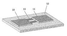
- FIG. 1 is a bird's-eye view showing an outline of the structure of the qubit device (hereinafter also simply referred to as “device”) of the first embodiment
- FIG. 2 is a top view of FIG. FIG.
- the originally opaque first qubit substrate 10 and second qubit substrate 11 are represented as transparent so that the arrangement of the superconducting wiring 13 is clear. ing.
- the device of the first embodiment has a structure in which a first qubit substrate 10 and a second qubit substrate 11 are flip-chip connected on a base substrate 12 having a superconducting wiring 13 extending in parallel.
- Superconducting flux qubits 14 are respectively disposed on the first qubit substrate 10 and the second qubit substrate 11, and each superconducting flux quanta is magnetically coupled to the superconducting flux qubit 14.
- a superconducting wiring 13 is arranged so as to surround the bit 14.
- the superconducting flux qubit 14 on the first qubit substrate 10 and the superconducting flux qubit 14 on the second qubit substrate 11 are magnetically coupled.
- 1 and 2 show the case where there is one superconducting loop for coupling the superconducting magnetic flux qubit 14, but a plurality of superconducting loops may be coupled in series.
- the material of the first qubit substrate 10, the second qubit substrate 11, and the base substrate 14 a material generally used as a substrate of a metal superconducting device such as silicon or sapphire can be used.
- a metal superconductor such as niobium, niobium nitride, aluminum, indium, rhenium, tantalum, or titanium nitride is used.
- a metal superconductor such as lead, tin, or indium or an alloy thereof is used.
- FIGS. 3A is a top view and FIG. 3B is a cross-sectional view of the central portion of FIG.
- the originally opaque first qubit substrate 10 and second qubit substrate 11 are represented as transparent so that the arrangement of the superconducting wiring 13 is clear.
- a first qubit substrate 10 and a second qubit substrate 11 are flip-chip connected by solder bumps 16 on a base substrate 12 having a superconducting wiring 13 forming one closed loop.
- the solder bumps 16 used for flip chip connection need not be superconductors.
- Superconducting flux qubits 14 are respectively disposed on the first qubit substrate 10 and the second qubit substrate 11, and each superconducting flux quanta is magnetically coupled to the superconducting flux qubit 14.
- a superconducting wiring 13 is arranged so as to surround the bit 14.
- the first qubit substrate 10 and the second qubit substrate 11 are flip-chip connected to the base base 12 plate so that each surface faces the surface of the base substrate 12, and superconductivity on the base substrate 12. There is a gap between the wiring 13 and the superconducting wiring 13 on the first qubit substrate 10 and the superconducting wiring 13 on the second qubit substrate 11.
- the three superconducting wirings 13 facing the gap can form a magnetic coupling via inductance.
- FIG. 4 is a (a) top view and (b) enlarged view of the central portion of the device for explaining the present embodiment.
- a superconducting flux qubit 14 that is a superconducting loop including the Josephson junction 17 is disposed on the base substrate 12.
- three superconducting flux qubits 14 are disposed on the base substrate 12 as an example, but the number is not limited to three and may include at least one or more.
- the superconducting flux qubit 14 on the base substrate 12 is connected to the superconducting flux qubit on the first qubit substrate 10 via the superconducting wiring 13. 14 and the superconducting flux qubit 14 on the second qubit substrate 11 can be magnetically coupled.
- the superconducting flux qubit 14 on the base substrate 12 is used as a part of the quantum annealing machine network, a more efficient network can be formed.
- this embodiment it becomes possible to arrange a plurality of substrates having superconducting flux qubits while maintaining strong coupling between superconducting flux qubits, and the quantum annealing machine can be placed in an area of one substrate or more. It becomes possible to expand.
- FIG. 5 is a bird's-eye view for explaining the fourth embodiment
- FIG. 6 is a view of the structure of FIG. 5 seen from the back side
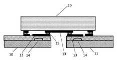
- FIGS. 7 and 8 are cross-sectional views in the vicinity of the center.
- the connection substrate 19 is flip-chip connected so as to straddle the first qubit substrate 10 and the second qubit substrate 11.
- the size (surface area) of the connection substrate 19 can be selected to be smaller than the sizes of the first qubit substrate 10 and the second qubit substrate 11.
- FIG. 6 when the structure of FIG.
- the arrangement of the superconducting wiring 13 similar to that of the first embodiment and the superconducting wiring 13 similar to that of the second embodiment are formed on the connection substrate 19. Either the arrangement or the arrangement of the superconducting wiring 13 and the superconducting flux qubit 14 similar to that of the third embodiment is selected and arranged.
- the superconducting wiring 13, the superconducting solder bump 15, the superconducting wiring 13 on the first qubit substrate, and the second conductor provided on the connection substrate 19 are shown.
- One continuous superconducting loop consisting of the superconducting wiring 13 on the qubit substrate 11 is formed.
- the superconducting flux qubit 14 magnetically coupled to the superconducting wiring 13 provided on the first qubit substrate 10 and the superconducting wiring provided on the second substrate 11 are used. 13 and the superconducting flux qubit 14 magnetically coupled can be coupled.
- the superconducting wiring 13 on the connection substrate 19 the superconducting wiring 13 on the first qubit substrate 10, and the superconducting wiring 13 on the second qubit substrate 11 are provided. It is also possible to remove the superconducting solder bump 15 in this portion as shown in the cross-sectional view of FIG.
- a superconducting flux qubit 14 which is a superconducting loop having a Josephson junction 17 is arranged on a connection substrate 19, and both ends thereof are connected via magnetic coupling.
- the superconducting wiring 13 can also be provided.
- the total surface area (size) of the first qubit substrate 10 and the second qubit substrate 11 needs to be smaller than the connection substrate 12.
- FIG. 9 is a bird's-eye view for explaining the fifth embodiment.
- the first qubit substrate 20 and the second qubit substrate 21 are flip-chip connected by a first connection substrate 24.
- the second qubit substrate 21 and the third qubit substrate 22 are flip-chip connected by a second connection substrate 25.
- the third qubit substrate 22 and the fourth qubit substrate 23 are flip-chip connected by a third connection substrate 26.
- the fourth qubit substrate 32 and the first qubit substrate 20 are flip-chip connected by a fourth connection substrate 27.
- the first connection board 24, the second connection board 25, the third connection board 26, and the fourth connection board 27 have the same structure as the connection board 19 described in the fourth embodiment. ing. All of the above structures are arranged on the base substrate 28.
- FIG. 10 is a diagram showing a partial cross-sectional structure of the first qubit substrate 20, the second qubit substrate 21, the first connection substrate 24, and the base substrate 28 of the present embodiment.
- the superconducting flux qubit 14 disposed on the first qubit substrate 20 and the superconducting flux qubit 14 disposed on the second qubit substrate 21 are superconducting on the first qubit substrate 20.
- the first to fourth connection boards have the same structure as the connection board 19 described in the fourth embodiment.
- the through-via 29 provided in the first qubit substrate 20, the second qubit substrate 21, the third qubit substrate 22, and the fourth qubit substrate 23 has a super A conductor or a metal having a high conductivity such as copper is filled using a technique such as plating.
- the power line, the input line, and the output line of the quantum annealing machine connected to the outside are connected to the first qubit substrate 20 and the second quantum from the base substrate 28 through the solder bump 30 and the through via 29 filled with metal. It is connected to the circuit on the bit board 21.
- the power supply necessary for the quantum annealing machine operation on the first qubit substrate 20, the second qubit substrate 21, the third qubit substrate 22, and the fourth qubit substrate 23 Wiring for lines, input lines, and output lines can be greatly reduced, and the installation area of the quantum annealing machine body can be increased.
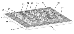
- FIG. 11 is a bird's-eye view for explaining the present embodiment.
- a first qubit substrate 31, a second qubit substrate 32, a third qubit substrate 33, and a fourth qubit substrate 34 are flip-chip connected to a first interposer substrate 35.
- the connections between the qubits provided on the four qubit substrates 31 to 34 are performed by using any one of the first embodiment, the second embodiment, and the third embodiment described above in the first interposer substrate 35, or This is done using a complex method.
- each of the second interposer substrate 36, the third interposer substrate 37, and the fourth interposer substrate 38 is flip-chip connected with four qubit substrates.
- the second interposer substrate 36 adjacent to the first interposer substrate 35 can couple the superconducting flux qubits 14 disposed on each other using the first connection substrate 39 flip-chip connected to both. it can.
- the connection of the superconducting flux qubits 14 provided on the first interposer substrate 35 and the second interposer substrate 36 is performed using the method described in the fourth embodiment.
- the second interposer substrate 36 and the third interposer substrate 37, the third interposer substrate 37 and the fourth interposer substrate 38, and the fourth interposer substrate 38 and the first interposer substrate 35 are respectively connected to the second connection.
- the first interposer substrate 35, the second interposer substrate 36, the third interposer substrate 37, and the fourth interposer substrate 38 are disposed on the base substrate 43.
- FIG. 12 is a partial cross-sectional view of the first interposer substrate 35, the first connection substrate 39, the second interposer substrate 36, and the base substrate 43.
- the first qubit substrate 31 and the second qubit substrate 32 are flip-chip connected to the first interposer substrate 35, and the superconducting flux qubit 14 installed on each substrate is the first implementation. Connected in the manner described in the form.
- the first interposer substrate 35 is connected by flip-chip connecting the second interposer substrate 36 to which the superconducting flux qubit substrate is flip-chip connected and the first connection substrate 39, and is connected to each interposer substrate.
- the superconducting flux qubits on the flip-chip connected qubit substrate are connected by a superconducting loop using the superconducting wiring 13 and superconducting solder bumps 15 as described in the first and fourth embodiments. Done.
- a through via 29 is provided in the first interposer substrate 35 and the second interposer substrate 36 and is placed on the base substrate 43 via the solder bumps 30.
- the power supply line, input line, and output line of the quantum annealing machine connected to the outside are connected from the base substrate 43 to the circuit on the interposer substrate through the solder bump 30 and the through via 29.
- the through-via is filled with a superconductor such as tin or a metal having a high conductivity such as copper using a technique such as plating.
- a quantum annealing machine in which a large number of qubit substrates are efficiently connected can be realized, and a large-scale quantum annealing machine far exceeding the number of qubits that can be mounted on one qubit substrate is realized. It becomes possible to do. Further, by repeating the structure of the present embodiment, a larger quantum annealing machine can be realized.
- the qubit device of the present invention can be industrially used as a quantum annealing machine capable of changing / expanding the number of qubits as required.
Landscapes
- Engineering & Computer Science (AREA)
- Superconductor Devices And Manufacturing Methods Thereof (AREA)
- General Physics & Mathematics (AREA)
- Theoretical Computer Science (AREA)
- Physics & Mathematics (AREA)
- Mathematical Analysis (AREA)
- Evolutionary Computation (AREA)
- Data Mining & Analysis (AREA)
- Condensed Matter Physics & Semiconductors (AREA)
- Mathematical Optimization (AREA)
- Pure & Applied Mathematics (AREA)
- Computing Systems (AREA)
- General Engineering & Computer Science (AREA)
- Mathematical Physics (AREA)
- Software Systems (AREA)
- Computational Mathematics (AREA)
- Artificial Intelligence (AREA)
Abstract
本発明の量子ビットデバイスは、第1の超伝導磁束量子ビット14と磁気的な結合部分を持つように配置された第1の超伝導配線13を表面に有する第1の量子ビット基板10と、第2の超伝導磁束量子ビット14と磁気的な結合部分を持つように配置された第2の超伝導配線13を表面に有する第2の量子ビット基板11と、並行に延びる2つの超伝導配線からなる第3の超伝導配線13を表面に有するベース基板12と、を備える。ベース基板上に第1及び第2の量子ビット基板が載置され、第1の超伝導配線の2つの端部と第3の超伝導配線の一方の2つの端部とが超伝導はんだ15を介して接合し、第2の超伝導配線の2つの端部と第3の超伝導配線の他方の2つの端部とが超伝導はんだ15を介して接合し、第1から第3の3つの超伝導配線線は1つの連続した超伝導ループを形成している。
Description
本発明は、量子力学的な重ね合わせ状態を利用する量子ビットを情報担体として用いる量子ビットデバイスに関する。
量子ビットを用いた情報処理装置として、ネットワーク接続された量子ビットの状態が結合の方法や結合の強さに応じてある安定状態に収束することを利用して最適化問題を解く量子アニーリング機械が知られている。従来の量子アニーリング機械に用いられている量子ビットは、ジョセフソン接合を有する超伝導ループに単一磁束量子(Φ0=2.07×10⁻¹⁵Wb)を蓄えるもので磁束量子ビットと呼ばれる。
磁束量子ビット同士の結合には、超伝導体で構成される閉じたループである超伝導ループが用いられる。超伝導ループは、超伝導体の反磁性効果によって外部から磁場が印加されるとループを循環する遮蔽電流が流れるという性質を有している。このため、磁束量子ビットを超伝導ループと磁気的に結合することによって、磁束量子ビットの状態に応じた遮蔽電流が超伝導ループに流れ、この超伝導ループに同様に磁気的に結合された他の磁束量子ビットの状態に影響を与えることができる。この手法により異なる磁束量子ビット間の結合を作ることができる。
非特許文献1にあるように、磁束量子ビットは二重井戸ポテンシャルを形成するために100pH程度の比較的大きなインダクタンスが必要であり、ジョセフソン接合の等価インダクタンスを有効に用いたとしても超伝導ループをあまり小さくすることができない。その結果、一つの基板上に搭載できる量子ビット数が多くとも数万個に限定されるという問題点がある。例えば、量子アニーリング機械は、非特許文献2にあるように、カナダのD-Wave System社から超伝導体を用いた量子コンピュータ(例えば、”D-Wave 2000Q”(登録商標))として製品化されている。しかし、使用されている量子ビット数が2000個程度であり、実用的な問題を解くために必要だと言われている100万量子ビットと比べると規模が圧倒的に小さいという問題点を有している。
複数個の基板を用いて量子ビット回路を構成するデバイス構造として、非特許文献3にあるものが知られている。このデバイスでは、スピン量子ビットが搭載された量子ビット基板は別基板に設けられた磁気結合カプラー上に載置され、磁気結合カプラーは貫通ビアを介して別基板上の配線と結合されている。このデバイス構造は量子ビット回路にフリップチップ接続や貫通ビアといった3次元デバイス構造を導入し、磁気結合カプラーや配線回路による量子ビット基板上の面積負荷を軽くすることによって、一つの基板に集積できる量子ビット数を向上できる利点はある。しかし、量子ビット基板と磁気結合カプラー基板のフリップチップ接続は1:1接続であり、一つの量子ビット基板以上に量子ビット数を増やすことはできない。
半導体デバイスでは、非特許文献4にあるように複数の基板をインターポーザと呼ばれるより大きな基板上にフリップチップ接続し、インターポーザを貫通ビアでプリント基板上の配線パターンと接続する3次元デバイス構造が知られている。また、特許文献1にあるような隣接するインターポーザをフリップチップ接続で連結するブリッジング・ブロック・コンタクトと呼ばれる手法も知られている。これらの手法を用いることで、デバイス規模を一つの基板内にとどまることなく水平方向に拡張することが可能となる。
前述したように磁束量子ビット同士の結合には、超伝導ループを用いた磁気接続回路を用いる必要がある。超伝導ループを用いた磁気接続回路は、磁束量子ビットの量子状態を損なうことなく他の磁束量子ビットと接続できる唯一の現実的な方法である。このため、半導体デバイスで用いられているデバイス構造を複数の量子ビット基板の接続に導入した場合、半導体デバイスで用いられている通常の導電体配線で接続する方法では、異なる基板上にある量子ビットを結合することができないという問題点があった。
山本剛、「ジョセフソン効果と量子ビット」電子情報通信学会、誌Vol. 95, pp. 750-753, 2012
カナダのD-Wave System社のホームページ:(http://www.dwavesys.com/)
W. Oliver, "Quantum Enhanced Optimization: Experimental Study Overview",10/26/2015 (https://www.iarpa.gov/images/files/programs/qeo/MIT_Lincoln_Laboratory_proposers_day_presentation_Will_Oliver.pdf)
電子情報技術マガジン「The Sound of Cadence」SEP 2011 Vol.2 (https://www.cadence.co.jp/soconline/vol2/tec4/all.html)
本発明は、上記した従来技術の諸問題を解決し、拡張性を有する量子ビットデバイスを提供することを目的とする。
本発明の一態様の量子ビットデバイスでは、第1の超伝導磁束量子ビットと磁気的な結合部分を持つように配置された第1の超伝導配線を表面に有する第1の量子ビット基板と、第2の超伝導磁束量子ビットと磁気的な結合部分を持つように配置された第2の超伝導配線を表面に有する第2の量子ビット基板と、並行に延びる2つの超伝導配線からなる第3の超伝導配線を表面に有するベース基板と、を備える。ベース基板上に第1及び第2の量子ビット基板が載置され、第1の超伝導配線の2つの端部と第3の超伝導配線の一方の2つの端部とが超伝導はんだを介して接合し、第2の超伝導配線の2つの端部と第3の超伝導配線の他方の2つの端部とが超伝導はんだを介して接合し、第1から第3の3つの超伝導配線は1つの連続した超伝導ループを形成している。
本発明の他の一態様の量子ビットデバイスでは、第1の超伝導磁束量子ビットと磁気的な結合部分を持つように配置された1つの閉ループをなす超伝導配線を含む第1の超伝導ループを表面に有する第1の量子ビット基板と、第2の超伝導磁束量子ビットと磁気的な結合部分を持つように配置された1つの閉ループをなす超伝導配線を含む第2の超伝導ループを表面に有する第2の量子ビット基板と、1つの閉ループをなす超伝導配線を含む第3の超伝導ループを表面に有するベース基板と、を備える。第1の量子ビット基板と第2の量子ビット基板は、各表面がベース基板の表面に対向するようにベース基板上にフリップチップ接続され、第1及び第2の超伝導ループは第3の超伝導ループと空隙を隔てて磁気的に結合することができる。
本発明の他の一態様の量子ビットデバイスでは、第1の超伝導磁束量子ビットと磁気的な結合部分を持つように配置された第1の超伝導配線を表面に有する第1の量子ビット基板と、第2の超伝導磁束量子ビットと磁気的な結合部分を持つように配置された第2の超伝導配線を表面に有する第2の量子ビット基板と、並行に延びる2つの超伝導配線からなる第3の超伝導配線を表面に有し、第1及び第2の量子ビット基板よりもサイズが小さい接続基板と、を備える。接続基板は、その表面が第1及び第2の量子ビット基板の表面に対向し、かつ第1の量子ビット基板と第2の量子ビット基板を跨ぐように載置され、第1の超伝導配線の2つの端部と第3の超伝導配線の一方の2つの端部とが超伝導はんだを介して接合し、第2の超伝導配線の2つの端部と第3の超伝導配線の他方の2つの端部とが超伝導はんだを介して接合し、第1から第3の3つの超伝導配線は1つの連続した超伝導ループを形成している。
本発明の他の一態様の量子ビットデバイスでは、第1の超伝導磁束量子ビットと磁気的な結合部分を持つように配置された1つの閉ループをなす超伝導配線を含む第1の超伝導ループを表面に有する第1の量子ビット基板と、第2の超伝導磁束量子ビットと磁気的な結合部分を持つように配置された1つの閉ループをなす超伝導配線を含む第2の超伝導ループを表面に有する第2の量子ビット基板と、1つの閉ループをなす超伝導配線を含む第3の超伝導ループを表面に有し、第1及び第2の量子ビット基板よりもサイズが小さい接続基板と、を備える。接続基板は、その表面が第1及び第2の量子ビット基板の表面に対向し、かつ第1の量子ビット基板と第2の量子ビット基板を跨ぐように、第1及び第2の量子ビット基板上にフリップチップ接続され、第1及び第2の超伝導ループは第3の超伝導ループと空隙を隔てて磁気的に結合することができる。
本発明の他の一態様の量子ビットデバイスでは、第1の超伝導磁束量子ビットと磁気的な結合部分を持つように配置された第1の超伝導配線を表面に有する第1の量子ビット基板と、第2の超伝導磁束量子ビットと磁気的な結合部分を持つように配置された第2の超伝導配線を表面に有する第2の量子ビット基板と、並行に延びる2つの超伝導配線からなる第3の超伝導配線を表面に有するインターポーザ基板と、インターポーザ基板を載置するベース基板と、を備える。インターポーザ基板上に第1及び第2の量子ビット基板が載置され、第1の超伝導配線の2つの端部と第3の超伝導配線の一方の2つの端部とが超伝導はんだを介して接合し、第2の超伝導配線の2つの端部と第3の超伝導配線の他方の2つの端部とが超伝導はんだを介して接合し、第1から第3の3つの超伝導配線は1つの連続した超伝導ループを形成し、ベース基板上の配線は、はんだを介してインターポーザ基板内の貫通導電ビア及びその上の配線に接続する。
図面を参照しながら本発明の実施形態について以下に説明する。
<第1実施形態>
図1と図2を参照しながら本発明の第1の実施形態の量子ビットデバイスの説明を行う。図1は第1の実施形態の量子ビットデバイス(以下、単に「デバイス」とも呼ぶ)の構造の概要を示した鳥瞰図であり、図2は図1の中央部分の(a)上面図と(b)断面図である。なお、図2の(a)上面図では、超伝導配線13の配置が明確になるように、本来不透明な第1の量子ビット基板10と第2の量子ビット基板11が透明なものとして表されている。第1の実施形態のデバイスは、第1の量子ビット基板10と第2の量子ビット基板11が、並行に伸びる超伝導配線13を有するベース基板12上にフリップチップ接続された構造を有する。第1の量子ビット基板10と第2の量子ビット基板11には、それぞれ超伝導磁束量子ビット14が配置され、さらに超伝導磁束量子ビット14と磁気的に結合するように、各超伝導磁束量子ビット14を囲む形で超伝導配線13が配置されている。
<第1実施形態>
図1と図2を参照しながら本発明の第1の実施形態の量子ビットデバイスの説明を行う。図1は第1の実施形態の量子ビットデバイス(以下、単に「デバイス」とも呼ぶ)の構造の概要を示した鳥瞰図であり、図2は図1の中央部分の(a)上面図と(b)断面図である。なお、図2の(a)上面図では、超伝導配線13の配置が明確になるように、本来不透明な第1の量子ビット基板10と第2の量子ビット基板11が透明なものとして表されている。第1の実施形態のデバイスは、第1の量子ビット基板10と第2の量子ビット基板11が、並行に伸びる超伝導配線13を有するベース基板12上にフリップチップ接続された構造を有する。第1の量子ビット基板10と第2の量子ビット基板11には、それぞれ超伝導磁束量子ビット14が配置され、さらに超伝導磁束量子ビット14と磁気的に結合するように、各超伝導磁束量子ビット14を囲む形で超伝導配線13が配置されている。
第1の量子ビット基板10上の超伝導配線13の2つの端部とベース基板12上の2つの超伝導配線13の一方の2つの端部とは、超伝導ハンダバンプ15介して接合している。同様に、第2の量子ビット基板11上の超伝導配線13の2つの端部とベース基板12上の2つの超伝導配線13の他方の2つの端部とは、超伝導ハンダバンプ15介して接合している。その結果、ベース基板12上の超伝導配線13および超伝導ハンダバンプ15、第1の量子ビット基板10上の超伝導配線13、および第2の量子ビット基板11上の超伝導配線13からなる1つの連続した超伝導ループが形成される。この超伝導ループによって、第1の量子ビット基板10上の超伝導磁束量子ビット14と、第2の量子ビット基板11上の超伝導磁束量子ビット14は、磁気的に結合される。なお、図1、図2には超伝導磁束量子ビット14を結合する超伝導ループは1個の場合が示されているが、複数個の超伝導ループが直列に結合されていてもよい。
第1の量子ビット基板10、第2の量子ビット基板11、及びベース基板14の材料には、例えばシリコンやサファイアなど一般に金属超伝導デバイスの基板として用いられる材料を使用することができる。超伝導磁束量子ビット14や超伝導配線13の材料としては、ニオブ、窒化ニオブ、アルミニウム、インジウム、レニウム、タンタル、窒化チタンなどの金属超伝導体が用いられる。超伝導ハンダバンプ15の材料としては、鉛、スズ、インジウムなどの金属超伝導体もしくはこれらの合金が用いられる。本実施形態を用いることにより、異なる基板上に存在する超伝導磁束量子ビット14を結合することが可能となり、量子アニーリング機械を一つの量子ビット基板以上の領域に拡張することが可能となる。
<第2実施形態>
図1と図3を用いて本発明の第2の実施形態の量子ビットデバイスの説明を行う。図3は、図1の中央部分の(a)上面図と(b)断面図である。なお、図3の(a)上面図では、超伝導配線13の配置が明確になるように、本来不透明な第1の量子ビット基板10と第2の量子ビット基板11が透明なものとして表されている。第2の実施形態のデバイスは、第1の量子ビット基板10と第2の量子ビット基板11が、1つの閉ループをなす超伝導配線13を有するベース基板12上に、ハンダバンプ16によりフリップチップ接続された構造を有する。ここで、フリップチップ接続に用いられるハンダバンプ16は超伝導体である必要はない。第1の量子ビット基板10と第2の量子ビット基板11には、それぞれ超伝導磁束量子ビット14が配置され、さらに超伝導磁束量子ビット14と磁気的に結合するように、各超伝導磁束量子ビット14を囲む形で超伝導配線13が配置されている。
図1と図3を用いて本発明の第2の実施形態の量子ビットデバイスの説明を行う。図3は、図1の中央部分の(a)上面図と(b)断面図である。なお、図3の(a)上面図では、超伝導配線13の配置が明確になるように、本来不透明な第1の量子ビット基板10と第2の量子ビット基板11が透明なものとして表されている。第2の実施形態のデバイスは、第1の量子ビット基板10と第2の量子ビット基板11が、1つの閉ループをなす超伝導配線13を有するベース基板12上に、ハンダバンプ16によりフリップチップ接続された構造を有する。ここで、フリップチップ接続に用いられるハンダバンプ16は超伝導体である必要はない。第1の量子ビット基板10と第2の量子ビット基板11には、それぞれ超伝導磁束量子ビット14が配置され、さらに超伝導磁束量子ビット14と磁気的に結合するように、各超伝導磁束量子ビット14を囲む形で超伝導配線13が配置されている。
第1の量子ビット基板10と第2の量子ビット基板11は、各表面がベース基板12の表面に対向するようにベース基12板上にフリップチップ接続されており、ベース基板12上の超伝導配線13と、第1の量子ビット基板10上の超伝導配線13および第2の量子ビット基板11上の超伝導配線13との間に空隙がある。その空隙に面する3つの超伝導配線13は、インダクタンスを介した磁気的な結合を形成することができる。本実施形態を用いることにより、第1実施形態において必須であった超伝導ハンダバンプ15を用いることなく、異なる基板上に存在する超伝導磁束量子ビット14を結合することが可能になり、量子アニーリング機械を一つの基板以上の領域に拡張することが可能となる。
<第3実施形態>
図4を用いて本発明の第3の実施形態の量子ビットデバイスの説明を行う。図4は、本実施形態を説明するためのデバイスの(a)上面図とその中央部の(b)拡大図である。本実施形態では、ベース基板12上にジョセフソン接合17を含む超伝導ループである超伝導磁束量子ビット14が配置される。図4では、例としてベース基板12上に3つの超伝導磁束量子ビット14が配置されているが、その数は3に限定されず少なくとも1つ以上を含むことができる。第1実施形態および第2実施形態として説明したように、ベース基板12上の超伝導磁束量子ビット14を、超伝導配線13を介して第1の量子ビット基板10上にある超伝導磁束量子ビット14と第2の量子ビット基板11上にある超伝導磁束量子ビット14とに磁気的に結合することができる。
図4を用いて本発明の第3の実施形態の量子ビットデバイスの説明を行う。図4は、本実施形態を説明するためのデバイスの(a)上面図とその中央部の(b)拡大図である。本実施形態では、ベース基板12上にジョセフソン接合17を含む超伝導ループである超伝導磁束量子ビット14が配置される。図4では、例としてベース基板12上に3つの超伝導磁束量子ビット14が配置されているが、その数は3に限定されず少なくとも1つ以上を含むことができる。第1実施形態および第2実施形態として説明したように、ベース基板12上の超伝導磁束量子ビット14を、超伝導配線13を介して第1の量子ビット基板10上にある超伝導磁束量子ビット14と第2の量子ビット基板11上にある超伝導磁束量子ビット14とに磁気的に結合することができる。
一般に超伝導磁束量子ビットを結合する超伝導ループの長さが増加すると結合の効率が劣化する問題点があるが、ベース基板12上に超伝導磁束量子ビット14を配置することによって、短距離の超伝導ループを用いて超伝導磁束量子ビット間を結合することが可能となり、超伝導磁束量子ビット間の結合効率が向上する。図4に示すように、ベース基板12上の超伝導磁束量子ビット14を複数個配置すれば、その間をベース基板上12上の超伝導ループ18で接続することによって超伝導ループ17の長さを短縮できるため、量子ビットの結合効率をさらに向上する。また、ベース基板12上の超伝導磁束量子ビット14を量子アニーリング機械ネットワークの一部として使用すれば、より効率的なネットワーク形成が可能となる。本実施形態を用いることにより、超伝導磁束量子ビットを有する複数の基板を超伝導磁束量子ビット間の強い結合を保ったまま配置することが可能となり、量子アニーリング機械を一つの基板以上の領域に拡張することが可能となる。
<第4実施形態>
図5、図6、図7、図8を用いて本発明の第4の実施形態の量子ビットデバイスの説明を行う。図5は第4の実施の形態を説明するための鳥瞰図、図6は図5の構造を裏側から見た図、図7と図8は中央付近の断面図である。本実施形態では、図5に示されるように、第1の量子ビット基板10と第2の量子ビット基板11を跨ぐ形で接続基板19がフリップチップ接続された構造を有する。接続基板19のサイズ(表面積)は、第1の量子ビット基板10及び第2の量子ビット基板11のサイズよりも小さいものを選択することができる。図5の構造を裏側から見た図6に示されるように、接続基板19上には、第1実施形態と同様な超伝導配線13の配置、第2実施形態と同様な超伝導配線13の配置、または第3実施形態と同様な超伝導配線13及び超伝導磁束量子ビット14の配置のいずれかが選択されて配置される。
図5、図6、図7、図8を用いて本発明の第4の実施形態の量子ビットデバイスの説明を行う。図5は第4の実施の形態を説明するための鳥瞰図、図6は図5の構造を裏側から見た図、図7と図8は中央付近の断面図である。本実施形態では、図5に示されるように、第1の量子ビット基板10と第2の量子ビット基板11を跨ぐ形で接続基板19がフリップチップ接続された構造を有する。接続基板19のサイズ(表面積)は、第1の量子ビット基板10及び第2の量子ビット基板11のサイズよりも小さいものを選択することができる。図5の構造を裏側から見た図6に示されるように、接続基板19上には、第1実施形態と同様な超伝導配線13の配置、第2実施形態と同様な超伝導配線13の配置、または第3実施形態と同様な超伝導配線13及び超伝導磁束量子ビット14の配置のいずれかが選択されて配置される。
図7の断面図では、第1実施形態と同様に、接続基板19に設けられた超伝導配線13、超伝導はんだバンプ15、第1の量子ビット基板上の超伝導配線13、および第2の量子ビット基板11上の超伝導配線13からなる1つの連続した超伝導ループが形成される。この超伝導ループを用いて、第1の量子ビット基板10に設けられた超伝導配線13と磁気的に結合した超伝導磁束量子ビット14と、第2の基板11上に設けられた超伝導配線13と磁気的に結合した超伝導磁束量子ビット14とを結合することができる。また、第2実施形態と同様に、接続基板19上の超伝導配線13と、第1の量子ビット基板10上の超伝導配線13および第2の量子ビット基板11上の超伝導配線13とを空隙を介して磁気的に結合し、図8の断面図に示すように、この部分の超伝導はんだバンプ15を除くこともできる。
図6に示すように、第3実施形態と同様に、接続基板19上にジョセフソン接合17を有する超伝導ループである超伝導磁束量子ビット14を配置し、その両端に磁気的な結合を介して超伝導配線13を設けることもできる。第1実施形態から第4実施形態で述べた構造では、第1の量子ビット基板10および第2の量子ビット基板11を合わせた表面積(サイズ)は、接続基板12より小さいことが必要であったが、本実施の形態を用いることにより、第1の量子ビット基板10および第2の量子ビット基板11として、接続基板17より表面積が大きな基板を用いることが可能となり、より規模の大きな量子アニーリング機械を構成することが可能となる。
<第5実施形態>
図9と図10を用いて本発明の第5の実施形態の量子ビットデバイスの説明を行う。図9は第5の実施形態を説明するための鳥瞰図である。図9において、第1の量子ビット基板20と第2の量子ビット基板21は、第1の接続基板24によりフリップチップ接続されている。同様に第2の量子ビット基板21と第3の量子ビット基板22は、第2の接続基板25によりフリップチップ接続されている。第3の量子ビット基板22と第4の量子ビット基板23は、第3の接続基板26によりフリップチップ接続されている。また、第4の量子ビット基板32と第1の量子ビット基板20は、第4の接続基板27によりフリップチップ接続されている。ここで、第1の接続基板24、第2の接続基板25、第3の接続基板26、及び第4の接続基板27は、第4の実施形態で述べた接続基板19と同じ構造を有している。以上の構造は全てベース基板28上に配置される。
図9と図10を用いて本発明の第5の実施形態の量子ビットデバイスの説明を行う。図9は第5の実施形態を説明するための鳥瞰図である。図9において、第1の量子ビット基板20と第2の量子ビット基板21は、第1の接続基板24によりフリップチップ接続されている。同様に第2の量子ビット基板21と第3の量子ビット基板22は、第2の接続基板25によりフリップチップ接続されている。第3の量子ビット基板22と第4の量子ビット基板23は、第3の接続基板26によりフリップチップ接続されている。また、第4の量子ビット基板32と第1の量子ビット基板20は、第4の接続基板27によりフリップチップ接続されている。ここで、第1の接続基板24、第2の接続基板25、第3の接続基板26、及び第4の接続基板27は、第4の実施形態で述べた接続基板19と同じ構造を有している。以上の構造は全てベース基板28上に配置される。
図10は本実施形態の第1の量子ビット基板20、第2の量子ビット基板21、第1の接続基板24、及びベース基板28の一部の断面構造を示した図である。第1の量子ビット基板20に配置された超伝導磁束量子ビット14と、第2の量子ビット基板21上に配置された超伝導磁束量子ビット14は、第1の量子ビット基板20上の超伝導配線13、第2の量子ビット基板21上の超伝導配線13、第1の接続基板24上の超伝導配線13および超伝導ハンダバンプ15から構成される超伝導ループを介して磁気的に結合される。ここで、第1から第4の接続基板は、第4実施形態で述べた接続基板19と同様の構造を有する。
第1の量子ビット基板20、第2の量子ビット基板21、第3の量子ビット基板22、及び第4の量子ビット基板23に設けられた貫通ビア29には、詳細は上述したスズ等の超伝導体もしくは銅等の導電率が大きな金属がメッキ等の手法を用いて充填される。外部と接続された量子アニーリング機械の電源ライン、入力ライン、出力ラインは、ベース基板28からハンダバンプ30と金属が充填された貫通ビア29を介して、第1の量子ビット基板20および第2の量子ビット基板21上の回路に接続される。本実施形態を用いることによって、第1の量子ビット基板20、第2の量子ビット基板21、第3の量子ビット基板22、及び第4の量子ビット基板23上の量子アニーリング機械動作に必要な電源ライン、入力ライン、出力ラインのための配線を大幅に削減することが可能となり、量子アニーリング機械本体の設置面積を広げることが可能になる。
<第6実施形態>
図11と図12を用いて本発明の第6の実施形態の量子ビットデバイスの説明を行う。図11は本実施形態を説明するための鳥瞰図である。図11において、第1の量子ビット基板31、第2の量子ビット基板32、第3の量子ビット基板33、及び第4の量子ビット基板34が、第1のインターポーザ基板35上にフリップチップ接続されている。これら4つの量子ビット基板31~34に設けられた量子ビット間の接続は、第1のインターポーザ基板35において、上述した第1実施形態、第2実施形態、第3実施形態のいずれかもしくはそれらが複合した方法を用いて行われる。第2のインターポーザ基板36、第3のインターポーザ基板37、第4のインターポーザ基板38も同様に4個ずつの量子ビット基板がフリップチップ接続されている。
図11と図12を用いて本発明の第6の実施形態の量子ビットデバイスの説明を行う。図11は本実施形態を説明するための鳥瞰図である。図11において、第1の量子ビット基板31、第2の量子ビット基板32、第3の量子ビット基板33、及び第4の量子ビット基板34が、第1のインターポーザ基板35上にフリップチップ接続されている。これら4つの量子ビット基板31~34に設けられた量子ビット間の接続は、第1のインターポーザ基板35において、上述した第1実施形態、第2実施形態、第3実施形態のいずれかもしくはそれらが複合した方法を用いて行われる。第2のインターポーザ基板36、第3のインターポーザ基板37、第4のインターポーザ基板38も同様に4個ずつの量子ビット基板がフリップチップ接続されている。
第1のインターポーザ基板35と隣接する第2のインターポーザ基板36は、両者にフリップチップ接続された第1の接続基板39を用いて、それぞれに配置された超伝導磁束量子ビット14を結合することができる。第1のインターポーザ基板35と第2のインターポーザ基板36上に設けられた超伝導磁束量子ビット14の接続は、第4の実施形態で記述された方法を用いて行われる。同様に第2のインターポーザ基板36と第3のインターポーザ基板37、第3のインターポーザ基板37と第4のインターポーザ基板38、第4のインターポーザ基板38と第1のインターポーザ基板35は、それぞれ第2の接続基板40、第3の接続基板41および第4の接続基板42をフリップチップ接続することにより、それぞれに設置された超伝導磁束量子ビットを接続することができる。これにより、16個の量子ビット基板に配置された超伝導磁束量子ビットが結合された大規模な量子アニーリング機械を構成することが可能となる。第1のインターポーザ基板35、第2のインターポーザ基板36、第3のインターポーザ基板37、及び第4のインターポーザ基板38は、ベース基板43上に配置される。
図12は、第1のインターポーザ基板35、第1の接続基板39、第2のインターポーザ基板36およびベース基板43の断面図の一部である。第1の量子ビット基板31と第2の量子ビット基板32は、第1のインターポーザ基板35にフリップチップ接続されており、それぞれの基板に設置された超伝導磁束量子ビット14は、第1の実施形態に記述された方法で接続されている。第1のインターポーザ基板35は、同様に超伝導磁束量子ビット基板がフリップチップ接続された第2のインターポーザ基板36と第1の接続基板39をフリップチップ接続することにより接続され、それぞれのインターポーザ基板にフリップチップ接続された量子ビット基板上の超伝導磁束量子ビットは、第1実施形態および第4実施形態で述べられたように超伝導配線13および超伝導ハンダバンプ15を用いた超伝導ループにより接続が行われる。
第1のインターポーザ基板35と第2のインターポーザ基板36には貫通ビア29が設けられ、ハンダバンプ30を介してベース基板43上に置かれる。外部と接続された量子アニーリング機械の電源ライン、入力ライン、出力ラインは、ベース基板43からハンダバンプ30と貫通ビア29を介してインターポーザ基板上の回路に接続される。ここで、貫通ビアには、スズ等の超伝導体もしくは銅等の導電率が大きな金属がメッキ等の手法を用いて充填される。本実施形態を用いることにより、多数の量子ビット基板が効率的に接続された量子アニーリング機械が実現でき、一つの量子ビット基板に搭載できる量子ビット数を遥かに上回る大規模な量子アニーリング機械を実現することが可能となる。また、本実施の形態の構造を繰り返すことによりさらに大きな量子アニーリング機械の実現も可能となる。
本発明の実施形態について、図を参照しながら説明をした。しかし、本発明はこれらの実施形態に限られるものではない。さらに、本発明はその趣旨を逸脱しない範囲で当業者の知識に基づき種々なる改良、修正、変形を加えた態様で実施できるものである。
本発明の量子ビットデバイスは、必要に応じて量子ビット数を可変/拡張できる量子アニーリング機械として産業上の利用が可能である。
10、20、31 第1の量子ビット基板
11、21、32 第2の量子ビット基板
12、28、43 ベース基板
13 超伝導配線
14 超伝導磁束量子ビット
15 超伝導ハンダバンプ
16、30 ハンダバンプ
17 ジョセフソン接合
18 超伝導ループ
19 接続基板
22、33 第3の量子ビット基板
23、34 第4の量子ビット基板
24、39 第1の接続基板
25、40 第2の接続基板
26、41 第3の接続基板
27、42 第4の接続基板
29 貫通ビア
35 第1のインターポーザ基板
36 第2のインターポーザ基板
37 第3のインターポーザ基板
38 第4のインターポーザ基板
11、21、32 第2の量子ビット基板
12、28、43 ベース基板
13 超伝導配線
14 超伝導磁束量子ビット
15 超伝導ハンダバンプ
16、30 ハンダバンプ
17 ジョセフソン接合
18 超伝導ループ
19 接続基板
22、33 第3の量子ビット基板
23、34 第4の量子ビット基板
24、39 第1の接続基板
25、40 第2の接続基板
26、41 第3の接続基板
27、42 第4の接続基板
29 貫通ビア
35 第1のインターポーザ基板
36 第2のインターポーザ基板
37 第3のインターポーザ基板
38 第4のインターポーザ基板
Claims (8)
- 第1の超伝導磁束量子ビットと磁気的な結合部分を持つように配置された第1の超伝導配線を表面に有する第1の量子ビット基板と、
第2の超伝導磁束量子ビットと磁気的な結合部分を持つように配置された第2の超伝導配線を表面に有する第2の量子ビット基板と、
並行に延びる2つの超伝導配線からなる第3の超伝導配線を表面に有するベース基板と、を備え、
ベース基板上に第1及び第2の量子ビット基板が載置され、第1の超伝導配線の2つの端部と第3の超伝導配線の一方の2つの端部とが超伝導はんだを介して接合し、第2の超伝導配線の2つの端部と第3の超伝導配線の他方の2つの端部とが超伝導はんだを介して接合し、第1から第3の3つの超伝導配線は1つの連続した超伝導ループを形成している、量子ビットデバイス。 - 第1の超伝導磁束量子ビットと磁気的な結合部分を持つように配置された1つの閉ループをなす超伝導配線を含む第1の超伝導ループを表面に有する第1の量子ビット基板と、
第2の超伝導磁束量子ビットと磁気的な結合部分を持つように配置された1つの閉ループをなす超伝導配線を含む第2の超伝導ループを表面に有する第2の量子ビット基板と、
1つの閉ループをなす超伝導配線を含む第3の超伝導ループを表面に有するベース基板と、を備え、
第1の量子ビット基板と第2の量子ビット基板は、各表面がベース基板の表面に対向するようにベース基板上にフリップチップ接続され、第1及び第2の超伝導ループは第3の超伝導ループと空隙を隔てて磁気的に結合することができる、量子ビットデバイス。 - 前記ベース基板の表面に、前記第1から第3の3つの超伝導ループの少なくとも1つと磁気的に結合可能に形成された少なくとも1つの第3の超伝導磁束量子ビットをさらに含む、請求項2に記載の量子ビットデバイス。
- 第1の超伝導磁束量子ビットと磁気的な結合部分を持つように配置された第1の超伝導配線を表面に有する第1の量子ビット基板と、
第2の超伝導磁束量子ビットと磁気的な結合部分を持つように配置された第2の超伝導配線を表面に有する第2の量子ビット基板と、
並行に延びる2つの超伝導配線からなる第3の超伝導配線を表面に有し、第1及び第2の量子ビット基板よりもサイズが小さい接続基板と、を備え、
接続基板は、その表面が第1及び第2の量子ビット基板の表面に対向し、かつ第1の量子ビット基板と第2の量子ビット基板を跨ぐように載置され、第1の超伝導配線の2つの端部と第3の超伝導配線の一方の2つの端部とが超伝導はんだを介して接合し、第2の超伝導配線の2つの端部と第3の超伝導配線の他方の2つの端部とが超伝導はんだを介して接合し、第1から第3の3つの超伝導配線は1つの連続した超伝導ループを形成している、量子ビットデバイス。 - 第1の超伝導磁束量子ビットと磁気的な結合部分を持つように配置された1つの閉ループをなす超伝導配線を含む第1の超伝導ループを表面に有する第1の量子ビット基板と、
第2の超伝導磁束量子ビットと磁気的な結合部分を持つように配置された1つの閉ループをなす超伝導配線を含む第2の超伝導ループを表面に有する第2の量子ビット基板と、
1つの閉ループをなす超伝導配線を含む第3の超伝導ループを表面に有し、第1及び第2の量子ビット基板よりもサイズが小さい接続基板と、を備え、
接続基板は、その表面が第1及び第2の量子ビット基板の表面に対向し、かつ第1の量子ビット基板と第2の量子ビット基板を跨ぐように、第1及び第2の量子ビット基板上にフリップチップ接続され、第1及び第2の超伝導ループは第3の超伝導ループと空隙を隔てて磁気的に結合することができる、量子ビットデバイス。 - 前記第1及び第2の量子ビット基板を載置するベース基板をさらに含み、ベース基板上の配線は、はんだを介して前記第1及び第2の量子ビット基板内の貫通導電ビア及びその上の配線に接続する、請求項4または5に記載の量子ビットデバイス。
- 第1の超伝導磁束量子ビットと磁気的な結合部分を持つように配置された第1の超伝導配線を表面に有する第1の量子ビット基板と、
第2の超伝導磁束量子ビットと磁気的な結合部分を持つように配置された第2の超伝導配線を表面に有する第2の量子ビット基板と、
並行に延びる2つの超伝導配線からなる第3の超伝導配線を表面に有するインターポーザ基板と、
インターポーザ基板を載置するベース基板と、を備え、
インターポーザ基板上に第1及び第2の量子ビット基板が載置され、第1の超伝導配線の2つの端部と第3の超伝導配線の一方の2つの端部とが超伝導はんだを介して接合し、第2の超伝導配線の2つの端部と第3の超伝導配線の他方の2つの端部とが超伝導はんだを介して接合し、第1から第3の3つの超伝導配線は1つの連続した超伝導ループを形成し、
ベース基板上の配線は、はんだを介してインターポーザ基板内の貫通導電ビア及びその上の配線に接続する、量子ビットデバイス。 - 前記第1及び第2の量子ビット基板が載置された前記インターポーザ基板を少なくとも2つ以上含み、隣接する2つの前記インターポーザ基板を跨ぐように載置され、かつフリップチップ接続された接続基板をさらに含み、
2つの前記インターポーザ基板上の超伝導配線は、接続基板上の対向する超伝導配線と超伝導はんだを介して接合する、請求項7に記載の量子ビットデバイス。
Priority Applications (2)
| Application Number | Priority Date | Filing Date | Title |
|---|---|---|---|
| US16/613,252 US11362257B2 (en) | 2017-05-16 | 2018-05-09 | Quantum bit device |
| JP2019519194A JP6757948B2 (ja) | 2017-05-16 | 2018-05-09 | 量子ビットデバイス |
Applications Claiming Priority (2)
| Application Number | Priority Date | Filing Date | Title |
|---|---|---|---|
| JP2017-097658 | 2017-05-16 | ||
| JP2017097658 | 2017-05-16 |
Publications (1)
| Publication Number | Publication Date |
|---|---|
| WO2018212041A1 true WO2018212041A1 (ja) | 2018-11-22 |
Family
ID=64273710
Family Applications (1)
| Application Number | Title | Priority Date | Filing Date |
|---|---|---|---|
| PCT/JP2018/017962 Ceased WO2018212041A1 (ja) | 2017-05-16 | 2018-05-09 | 量子ビットデバイス |
Country Status (3)
| Country | Link |
|---|---|
| US (1) | US11362257B2 (ja) |
| JP (1) | JP6757948B2 (ja) |
| WO (1) | WO2018212041A1 (ja) |
Cited By (24)
| Publication number | Priority date | Publication date | Assignee | Title |
|---|---|---|---|---|
| JP2020511794A (ja) * | 2017-03-13 | 2020-04-16 | グーグル エルエルシー | 積層型量子コンピューティングデバイスにおける回路要素の集積 |
| WO2020146062A1 (en) * | 2019-01-07 | 2020-07-16 | Northrop Grumman Systems Corporation | Superconducting bump bond electrical characterization |
| WO2020164864A1 (en) * | 2019-02-11 | 2020-08-20 | International Business Machines Corporation | Cold-welded flip chip interconnect structure |
| WO2020254055A1 (en) * | 2019-06-17 | 2020-12-24 | International Business Machines Corporation | Superconducting interposer for the transmission of quantum information for quantum error correction |
| WO2020254036A1 (en) * | 2019-06-21 | 2020-12-24 | International Business Machines Corporation | Modular, frequency-flexible, superconducting quantum processor architecture |
| WO2021105119A1 (en) * | 2019-11-27 | 2021-06-03 | International Business Machines Corporation | Permanent wafer handlers with through silicon vias for thermalization and qubit modification |
| WO2021115988A1 (en) * | 2019-12-11 | 2021-06-17 | International Business Machines Corporation | Highway jumper to enable long range connectivity for superconducting quantum computer chip |
| JP2021158138A (ja) * | 2020-03-25 | 2021-10-07 | 株式会社神戸製鋼所 | 量子ビット集積装置 |
| JP2022002235A (ja) * | 2020-06-19 | 2022-01-06 | 日本電気株式会社 | 量子デバイス |
| JP2022002237A (ja) * | 2020-06-19 | 2022-01-06 | 日本電気株式会社 | 量子デバイス及びその製造方法 |
| JP2022041642A (ja) * | 2020-09-01 | 2022-03-11 | 国立研究開発法人産業技術総合研究所 | 3次元積層構造体 |
| US11417819B2 (en) | 2020-04-27 | 2022-08-16 | Microsoft Technology Licensing, Llc | Forming a bumpless superconductor device by bonding two substrates via a dielectric layer |
| JP2022537094A (ja) * | 2019-06-19 | 2022-08-24 | インターナショナル・ビジネス・マシーンズ・コーポレーション | 量子コンピューティング・デバイス用のトランズモン・キュービット・フリップチップ構造体の製造 |
| JP2022176437A (ja) * | 2021-05-17 | 2022-11-30 | 日本電気株式会社 | 超伝導デバイス |
| JP2023069792A (ja) * | 2021-11-08 | 2023-05-18 | 日本電気株式会社 | 量子デバイス |
| JP2023105034A (ja) * | 2020-06-05 | 2023-07-28 | 日本電気株式会社 | 量子デバイス及び量子計算機 |
| US11805708B2 (en) | 2020-06-19 | 2023-10-31 | Nec Corporation | Quantum device |
| EP4059056A4 (en) * | 2019-11-11 | 2024-01-10 | The Trustees of Princeton University | SUPERCONDUCTING QUANTUM BITS BASED ON TANTALUM |
| WO2024063165A1 (ja) * | 2022-09-22 | 2024-03-28 | 国立研究開発法人産業技術総合研究所 | 回路、超伝導装置及び回路の製造方法 |
| WO2024154358A1 (ja) | 2023-01-20 | 2024-07-25 | 富士通株式会社 | デバイスおよびデバイスの製造方法 |
| WO2024154354A1 (ja) | 2023-01-20 | 2024-07-25 | 富士通株式会社 | デバイスおよびデバイスの製造方法 |
| US12094812B2 (en) | 2020-06-19 | 2024-09-17 | Nec Corporation | Quantum device having quantum chip on interposer in contact with sample stage |
| US12108690B2 (en) | 2020-06-19 | 2024-10-01 | Nec Corporation | Quantum device |
| EP4709129A1 (en) | 2024-08-29 | 2026-03-11 | Fujitsu Limited | Quantum bit device and method for manufacturing quantum bit device |
Families Citing this family (3)
| Publication number | Priority date | Publication date | Assignee | Title |
|---|---|---|---|---|
| US20220199507A1 (en) * | 2020-12-22 | 2022-06-23 | International Business Machines Corporation | Multi-layered packaging for superconducting quantum circuits |
| EP4365937A4 (en) * | 2021-06-28 | 2025-06-04 | Origin Quantum Computing Technology (Hefei) Co., Ltd | QUANTUM DEVICE AND MANUFACTURING METHOD THEREFOR, AND ELECTRONIC DEVICE |
| FR3129772B1 (fr) * | 2021-11-30 | 2024-10-04 | Commissariat Energie Atomique | Structure d’intégration destinée à connecter une pluralité de dispositifs semi-conducteurs, procédés, assemblage et système associés |
Citations (3)
| Publication number | Priority date | Publication date | Assignee | Title |
|---|---|---|---|---|
| JPH06318741A (ja) * | 1992-03-09 | 1994-11-15 | Kyocera Corp | 配線基板 |
| JP2001101930A (ja) * | 1999-09-29 | 2001-04-13 | Internatl Superconductivity Technology Center | 酸化物超電導積層基板とその製造方法及び超電導集積回路の製造方法 |
| JP2015015590A (ja) * | 2013-07-04 | 2015-01-22 | 日本電信電話株式会社 | 光を用いた超伝導量子ビットの状態検出 |
Family Cites Families (4)
| Publication number | Priority date | Publication date | Assignee | Title |
|---|---|---|---|---|
| US6613463B1 (en) | 1999-09-06 | 2003-09-02 | International Superconductivity Technology Center | Superconducting laminated oxide substrate and superconducting integrated circuit |
| US7932515B2 (en) * | 2008-01-03 | 2011-04-26 | D-Wave Systems Inc. | Quantum processor |
| US20140131854A1 (en) | 2012-11-13 | 2014-05-15 | Lsi Corporation | Multi-chip module connection by way of bridging blocks |
| US10134972B2 (en) * | 2015-07-23 | 2018-11-20 | Massachusetts Institute Of Technology | Qubit and coupler circuit structures and coupling techniques |
-
2018
- 2018-05-09 US US16/613,252 patent/US11362257B2/en active Active
- 2018-05-09 JP JP2019519194A patent/JP6757948B2/ja active Active
- 2018-05-09 WO PCT/JP2018/017962 patent/WO2018212041A1/ja not_active Ceased
Patent Citations (3)
| Publication number | Priority date | Publication date | Assignee | Title |
|---|---|---|---|---|
| JPH06318741A (ja) * | 1992-03-09 | 1994-11-15 | Kyocera Corp | 配線基板 |
| JP2001101930A (ja) * | 1999-09-29 | 2001-04-13 | Internatl Superconductivity Technology Center | 酸化物超電導積層基板とその製造方法及び超電導集積回路の製造方法 |
| JP2015015590A (ja) * | 2013-07-04 | 2015-01-22 | 日本電信電話株式会社 | 光を用いた超伝導量子ビットの状態検出 |
Cited By (57)
| Publication number | Priority date | Publication date | Assignee | Title |
|---|---|---|---|---|
| JP2020511794A (ja) * | 2017-03-13 | 2020-04-16 | グーグル エルエルシー | 積層型量子コンピューティングデバイスにおける回路要素の集積 |
| US12217129B2 (en) | 2017-03-13 | 2025-02-04 | Google Llc | Integrating circuit elements in a stacked quantum computing device |
| US11436516B2 (en) | 2017-03-13 | 2022-09-06 | Google Llc | Integrating circuit elements in a stacked quantum computing device |
| US12033029B2 (en) | 2017-03-13 | 2024-07-09 | Google Llc | Integrating circuit elements in a stacked quantum computing device |
| WO2020146062A1 (en) * | 2019-01-07 | 2020-07-16 | Northrop Grumman Systems Corporation | Superconducting bump bond electrical characterization |
| US10950778B2 (en) | 2019-01-07 | 2021-03-16 | Northrop Grumman Systems Corporation | Superconducting bump bond electrical characterization |
| US11616187B2 (en) | 2019-01-07 | 2023-03-28 | Northrop Grumman Systems Corporation | Superconducting bump bond electrical characterization |
| US11165010B2 (en) | 2019-02-11 | 2021-11-02 | International Business Machines Corporation | Cold-welded flip chip interconnect structure |
| JP7394857B2 (ja) | 2019-02-11 | 2023-12-08 | インターナショナル・ビジネス・マシーンズ・コーポレーション | 冷間溶接フリップチップ相互接続構造 |
| CN113412541A (zh) * | 2019-02-11 | 2021-09-17 | 国际商业机器公司 | 冷焊接倒装芯片互连结构 |
| WO2020164864A1 (en) * | 2019-02-11 | 2020-08-20 | International Business Machines Corporation | Cold-welded flip chip interconnect structure |
| JP2022519443A (ja) * | 2019-02-11 | 2022-03-24 | インターナショナル・ビジネス・マシーンズ・コーポレーション | 冷間溶接フリップチップ相互接続構造 |
| US11875225B2 (en) | 2019-06-17 | 2024-01-16 | International Business Machines Corporation | Superconducting interposer for the transmission of quantum information for quantum error correction |
| US10984335B2 (en) | 2019-06-17 | 2021-04-20 | International Business Machines Corporation | Superconducting interposer for the transmission of quantum information for quantum error correction |
| US11537929B2 (en) | 2019-06-17 | 2022-12-27 | International Business Machines Corporation | Superconducting interposer for the transmission of quantum information for quantum error correction |
| WO2020254055A1 (en) * | 2019-06-17 | 2020-12-24 | International Business Machines Corporation | Superconducting interposer for the transmission of quantum information for quantum error correction |
| JP7479394B2 (ja) | 2019-06-19 | 2024-05-08 | インターナショナル・ビジネス・マシーンズ・コーポレーション | 量子コンピューティング・デバイス用のトランズモン・キュービット・フリップチップ構造体の製造 |
| JP2022537094A (ja) * | 2019-06-19 | 2022-08-24 | インターナショナル・ビジネス・マシーンズ・コーポレーション | 量子コンピューティング・デバイス用のトランズモン・キュービット・フリップチップ構造体の製造 |
| US11288587B2 (en) | 2019-06-21 | 2022-03-29 | International Business Machines Corporation | Modular, frequency-flexible, superconducting quantum processor architecture |
| CN113841166B (zh) * | 2019-06-21 | 2024-12-10 | 国际商业机器公司 | 模块化、频率灵活的超导量子处理器架构 |
| WO2020254036A1 (en) * | 2019-06-21 | 2020-12-24 | International Business Machines Corporation | Modular, frequency-flexible, superconducting quantum processor architecture |
| CN113841166A (zh) * | 2019-06-21 | 2021-12-24 | 国际商业机器公司 | 模块化、频率灵活的超导量子处理器架构 |
| EP4059056A4 (en) * | 2019-11-11 | 2024-01-10 | The Trustees of Princeton University | SUPERCONDUCTING QUANTUM BITS BASED ON TANTALUM |
| US11158781B2 (en) | 2019-11-27 | 2021-10-26 | International Business Machines Corporation | Permanent wafer handlers with through silicon vias for thermalization and qubit modification |
| WO2021105119A1 (en) * | 2019-11-27 | 2021-06-03 | International Business Machines Corporation | Permanent wafer handlers with through silicon vias for thermalization and qubit modification |
| US12550761B2 (en) | 2019-12-11 | 2026-02-10 | International Business Machines Corporation | Highway jumper to enable long range connectivity for superconducting quantum computer chip |
| US11568296B2 (en) | 2019-12-11 | 2023-01-31 | International Business Machines Corporation | Highway jumper to enable long range connectivity for superconducting quantum computer chip |
| JP2023505418A (ja) * | 2019-12-11 | 2023-02-09 | インターナショナル・ビジネス・マシーンズ・コーポレーション | 超伝導量子コンピュータ・チップ用のロングレンジ接続を可能にするハイウエイ・ジャンパ |
| WO2021115988A1 (en) * | 2019-12-11 | 2021-06-17 | International Business Machines Corporation | Highway jumper to enable long range connectivity for superconducting quantum computer chip |
| JP7619738B2 (ja) | 2019-12-11 | 2025-01-22 | インターナショナル・ビジネス・マシーンズ・コーポレーション | 超伝導量子コンピュータ・チップ用のロングレンジ接続を可能にするハイウエイ・ジャンパ |
| JP7516085B2 (ja) | 2020-03-25 | 2024-07-16 | 株式会社神戸製鋼所 | 量子ビット集積装置 |
| JP2021158138A (ja) * | 2020-03-25 | 2021-10-07 | 株式会社神戸製鋼所 | 量子ビット集積装置 |
| US11417819B2 (en) | 2020-04-27 | 2022-08-16 | Microsoft Technology Licensing, Llc | Forming a bumpless superconductor device by bonding two substrates via a dielectric layer |
| JP2023105034A (ja) * | 2020-06-05 | 2023-07-28 | 日本電気株式会社 | 量子デバイス及び量子計算機 |
| JP7605247B2 (ja) | 2020-06-05 | 2024-12-24 | 日本電気株式会社 | 量子デバイス及び量子計算機 |
| US12505371B2 (en) | 2020-06-05 | 2025-12-23 | Nec Corporation | Quantum device and quantum computer |
| US11805708B2 (en) | 2020-06-19 | 2023-10-31 | Nec Corporation | Quantum device |
| JP7501140B2 (ja) | 2020-06-19 | 2024-06-18 | 日本電気株式会社 | 量子デバイス |
| US12588530B2 (en) | 2020-06-19 | 2026-03-24 | Nec Corporation | Quantum device |
| JP2022002235A (ja) * | 2020-06-19 | 2022-01-06 | 日本電気株式会社 | 量子デバイス |
| JP2022002237A (ja) * | 2020-06-19 | 2022-01-06 | 日本電気株式会社 | 量子デバイス及びその製造方法 |
| JP7528557B2 (ja) | 2020-06-19 | 2024-08-06 | 日本電気株式会社 | 量子デバイス及びその製造方法 |
| US12094812B2 (en) | 2020-06-19 | 2024-09-17 | Nec Corporation | Quantum device having quantum chip on interposer in contact with sample stage |
| US12108690B2 (en) | 2020-06-19 | 2024-10-01 | Nec Corporation | Quantum device |
| US11871682B2 (en) | 2020-06-19 | 2024-01-09 | Nec Corporation | Quantum device and method of manufacturing the same |
| JP7523117B2 (ja) | 2020-09-01 | 2024-07-26 | 国立研究開発法人産業技術総合研究所 | 3次元積層構造体 |
| JP2022041642A (ja) * | 2020-09-01 | 2022-03-11 | 国立研究開発法人産業技術総合研究所 | 3次元積層構造体 |
| JP2022176437A (ja) * | 2021-05-17 | 2022-11-30 | 日本電気株式会社 | 超伝導デバイス |
| JP7703895B2 (ja) | 2021-05-17 | 2025-07-08 | 日本電気株式会社 | 超伝導デバイス |
| JP2023069792A (ja) * | 2021-11-08 | 2023-05-18 | 日本電気株式会社 | 量子デバイス |
| JP7782215B2 (ja) | 2021-11-08 | 2025-12-09 | 日本電気株式会社 | 量子デバイス |
| WO2024063165A1 (ja) * | 2022-09-22 | 2024-03-28 | 国立研究開発法人産業技術総合研究所 | 回路、超伝導装置及び回路の製造方法 |
| EP4654808A1 (en) | 2023-01-20 | 2025-11-26 | Fujitsu Limited | Device and method for producing device |
| EP4654809A1 (en) | 2023-01-20 | 2025-11-26 | Fujitsu Limited | Device and method for manufacturing device |
| WO2024154354A1 (ja) | 2023-01-20 | 2024-07-25 | 富士通株式会社 | デバイスおよびデバイスの製造方法 |
| WO2024154358A1 (ja) | 2023-01-20 | 2024-07-25 | 富士通株式会社 | デバイスおよびデバイスの製造方法 |
| EP4709129A1 (en) | 2024-08-29 | 2026-03-11 | Fujitsu Limited | Quantum bit device and method for manufacturing quantum bit device |
Also Published As
| Publication number | Publication date |
|---|---|
| US20210167271A1 (en) | 2021-06-03 |
| US11362257B2 (en) | 2022-06-14 |
| JP6757948B2 (ja) | 2020-09-23 |
| JPWO2018212041A1 (ja) | 2020-03-19 |
Similar Documents
| Publication | Publication Date | Title |
|---|---|---|
| JP6757948B2 (ja) | 量子ビットデバイス | |
| KR102250155B1 (ko) | 적층된 양자 디바이스들에서의 손실 감소 | |
| Das et al. | Cryogenic qubit integration for quantum computing | |
| JP6749382B2 (ja) | 超伝導デバイスにおける磁束制御 | |
| Das et al. | Large scale cryogenic integration approach for superconducting high-performance computing | |
| CN110176532A (zh) | 用于量子位器件的具有顶部超导体层的封装衬底 | |
| KR20130102052A (ko) | 열 관리를 갖춘 적층형 반도체 칩 장치 | |
| US12424604B2 (en) | Systems and methods for assembling processor systems | |
| KR20130097766A (ko) | 용장성 실리콘 관통 비아를 구비한 반도체 칩 | |
| GB2582527A (en) | Low loss architecture for superconducting qubit circuits | |
| KR102360801B1 (ko) | 열 전도성 열 싱크를 갖는 초전도 디바이스 | |
| US9466643B2 (en) | Ground grid for superconducting circuits | |
| EP4066279B1 (en) | Permanent wafer handlers with through silicon vias for thermalization and qubit modification | |
| US9105989B2 (en) | Connection structure, wiring substrate unit, electronic circuit part unit, and electronic apparatus | |
| JP2022519443A (ja) | 冷間溶接フリップチップ相互接続構造 | |
| JPWO2009048154A1 (ja) | 半導体装置及びその設計方法 | |
| CN113420884A (zh) | 一种量子芯片、量子计算机及量子芯片制备方法 | |
| Das et al. | Interconnect scheme for die-to-die and die-to-wafer-level heterogeneous integration for high-performance computing | |
| JP7619738B2 (ja) | 超伝導量子コンピュータ・チップ用のロングレンジ接続を可能にするハイウエイ・ジャンパ | |
| JP2005064028A (ja) | 配線基板 | |
| US20230200263A1 (en) | Quantum Bit Chip and Method for Fabricating Quantum Bit Chip | |
| Sakai et al. | Design and demonstration of large 2.5 D glass interposer for high bandwidth applications | |
| JP5618286B2 (ja) | 電流比較器 | |
| US20250372526A1 (en) | Interposer devices with mutliple interposer cores | |
| KR101232645B1 (ko) | 전원 핀을 포함하는 3차원 집적 회로 및 3차원 집적 회로의 전원 핀 배치 방법 |
Legal Events
| Date | Code | Title | Description |
|---|---|---|---|
| 121 | Ep: the epo has been informed by wipo that ep was designated in this application |
Ref document number: 18802988 Country of ref document: EP Kind code of ref document: A1 |
|
| ENP | Entry into the national phase |
Ref document number: 2019519194 Country of ref document: JP Kind code of ref document: A |
|
| NENP | Non-entry into the national phase |
Ref country code: DE |
|
| 122 | Ep: pct application non-entry in european phase |
Ref document number: 18802988 Country of ref document: EP Kind code of ref document: A1 |