WO2018216573A1 - 電磁波検出装置および情報取得システム - Google Patents
電磁波検出装置および情報取得システム Download PDFInfo
- Publication number
- WO2018216573A1 WO2018216573A1 PCT/JP2018/018954 JP2018018954W WO2018216573A1 WO 2018216573 A1 WO2018216573 A1 WO 2018216573A1 JP 2018018954 W JP2018018954 W JP 2018018954W WO 2018216573 A1 WO2018216573 A1 WO 2018216573A1
- Authority
- WO
- WIPO (PCT)
- Prior art keywords
- electromagnetic wave
- detection
- unit
- axis
- detection device
- Prior art date
- Legal status (The legal status is an assumption and is not a legal conclusion. Google has not performed a legal analysis and makes no representation as to the accuracy of the status listed.)
- Ceased
Links
Images

Classifications
-
- G—PHYSICS
- G01—MEASURING; TESTING
- G01S—RADIO DIRECTION-FINDING; RADIO NAVIGATION; DETERMINING DISTANCE OR VELOCITY BY USE OF RADIO WAVES; LOCATING OR PRESENCE-DETECTING BY USE OF THE REFLECTION OR RERADIATION OF RADIO WAVES; ANALOGOUS ARRANGEMENTS USING OTHER WAVES
- G01S17/00—Systems using the reflection or reradiation of electromagnetic waves other than radio waves, e.g. lidar systems
- G01S17/02—Systems using the reflection of electromagnetic waves other than radio waves
- G01S17/06—Systems determining position data of a target
- G01S17/08—Systems determining position data of a target for measuring distance only
- G01S17/10—Systems determining position data of a target for measuring distance only using transmission of interrupted, pulse-modulated waves
-
- G—PHYSICS
- G01—MEASURING; TESTING
- G01S—RADIO DIRECTION-FINDING; RADIO NAVIGATION; DETERMINING DISTANCE OR VELOCITY BY USE OF RADIO WAVES; LOCATING OR PRESENCE-DETECTING BY USE OF THE REFLECTION OR RERADIATION OF RADIO WAVES; ANALOGOUS ARRANGEMENTS USING OTHER WAVES
- G01S7/00—Details of systems according to groups G01S13/00, G01S15/00, G01S17/00
- G01S7/48—Details of systems according to groups G01S13/00, G01S15/00, G01S17/00 of systems according to group G01S17/00
- G01S7/483—Details of pulse systems
- G01S7/486—Receivers
- G01S7/4861—Circuits for detection, sampling, integration or read-out
-
- G—PHYSICS
- G01—MEASURING; TESTING
- G01S—RADIO DIRECTION-FINDING; RADIO NAVIGATION; DETERMINING DISTANCE OR VELOCITY BY USE OF RADIO WAVES; LOCATING OR PRESENCE-DETECTING BY USE OF THE REFLECTION OR RERADIATION OF RADIO WAVES; ANALOGOUS ARRANGEMENTS USING OTHER WAVES
- G01S17/00—Systems using the reflection or reradiation of electromagnetic waves other than radio waves, e.g. lidar systems
- G01S17/02—Systems using the reflection of electromagnetic waves other than radio waves
- G01S17/06—Systems determining position data of a target
-
- G—PHYSICS
- G01—MEASURING; TESTING
- G01S—RADIO DIRECTION-FINDING; RADIO NAVIGATION; DETERMINING DISTANCE OR VELOCITY BY USE OF RADIO WAVES; LOCATING OR PRESENCE-DETECTING BY USE OF THE REFLECTION OR RERADIATION OF RADIO WAVES; ANALOGOUS ARRANGEMENTS USING OTHER WAVES
- G01S17/00—Systems using the reflection or reradiation of electromagnetic waves other than radio waves, e.g. lidar systems
- G01S17/02—Systems using the reflection of electromagnetic waves other than radio waves
- G01S17/06—Systems determining position data of a target
- G01S17/08—Systems determining position data of a target for measuring distance only
-
- G—PHYSICS
- G01—MEASURING; TESTING
- G01S—RADIO DIRECTION-FINDING; RADIO NAVIGATION; DETERMINING DISTANCE OR VELOCITY BY USE OF RADIO WAVES; LOCATING OR PRESENCE-DETECTING BY USE OF THE REFLECTION OR RERADIATION OF RADIO WAVES; ANALOGOUS ARRANGEMENTS USING OTHER WAVES
- G01S17/00—Systems using the reflection or reradiation of electromagnetic waves other than radio waves, e.g. lidar systems
- G01S17/02—Systems using the reflection of electromagnetic waves other than radio waves
- G01S17/06—Systems determining position data of a target
- G01S17/42—Simultaneous measurement of distance and other co-ordinates
-
- G—PHYSICS
- G01—MEASURING; TESTING
- G01S—RADIO DIRECTION-FINDING; RADIO NAVIGATION; DETERMINING DISTANCE OR VELOCITY BY USE OF RADIO WAVES; LOCATING OR PRESENCE-DETECTING BY USE OF THE REFLECTION OR RERADIATION OF RADIO WAVES; ANALOGOUS ARRANGEMENTS USING OTHER WAVES
- G01S17/00—Systems using the reflection or reradiation of electromagnetic waves other than radio waves, e.g. lidar systems
- G01S17/86—Combinations of lidar systems with systems other than lidar, radar or sonar, e.g. with direction finders
-
- G—PHYSICS
- G01—MEASURING; TESTING
- G01S—RADIO DIRECTION-FINDING; RADIO NAVIGATION; DETERMINING DISTANCE OR VELOCITY BY USE OF RADIO WAVES; LOCATING OR PRESENCE-DETECTING BY USE OF THE REFLECTION OR RERADIATION OF RADIO WAVES; ANALOGOUS ARRANGEMENTS USING OTHER WAVES
- G01S17/00—Systems using the reflection or reradiation of electromagnetic waves other than radio waves, e.g. lidar systems
- G01S17/88—Lidar systems specially adapted for specific applications
- G01S17/89—Lidar systems specially adapted for specific applications for mapping or imaging
-
- G—PHYSICS
- G01—MEASURING; TESTING
- G01S—RADIO DIRECTION-FINDING; RADIO NAVIGATION; DETERMINING DISTANCE OR VELOCITY BY USE OF RADIO WAVES; LOCATING OR PRESENCE-DETECTING BY USE OF THE REFLECTION OR RERADIATION OF RADIO WAVES; ANALOGOUS ARRANGEMENTS USING OTHER WAVES
- G01S7/00—Details of systems according to groups G01S13/00, G01S15/00, G01S17/00
- G01S7/48—Details of systems according to groups G01S13/00, G01S15/00, G01S17/00 of systems according to group G01S17/00
- G01S7/481—Constructional features, e.g. arrangements of optical elements
- G01S7/4816—Constructional features, e.g. arrangements of optical elements of receivers alone
-
- G—PHYSICS
- G01—MEASURING; TESTING
- G01S—RADIO DIRECTION-FINDING; RADIO NAVIGATION; DETERMINING DISTANCE OR VELOCITY BY USE OF RADIO WAVES; LOCATING OR PRESENCE-DETECTING BY USE OF THE REFLECTION OR RERADIATION OF RADIO WAVES; ANALOGOUS ARRANGEMENTS USING OTHER WAVES
- G01S7/00—Details of systems according to groups G01S13/00, G01S15/00, G01S17/00
- G01S7/48—Details of systems according to groups G01S13/00, G01S15/00, G01S17/00 of systems according to group G01S17/00
- G01S7/481—Constructional features, e.g. arrangements of optical elements
- G01S7/4817—Constructional features, e.g. arrangements of optical elements relating to scanning
-
- G—PHYSICS
- G01—MEASURING; TESTING
- G01S—RADIO DIRECTION-FINDING; RADIO NAVIGATION; DETERMINING DISTANCE OR VELOCITY BY USE OF RADIO WAVES; LOCATING OR PRESENCE-DETECTING BY USE OF THE REFLECTION OR RERADIATION OF RADIO WAVES; ANALOGOUS ARRANGEMENTS USING OTHER WAVES
- G01S7/00—Details of systems according to groups G01S13/00, G01S15/00, G01S17/00
- G01S7/48—Details of systems according to groups G01S13/00, G01S15/00, G01S17/00 of systems according to group G01S17/00
- G01S7/497—Means for monitoring or calibrating
-
- G—PHYSICS
- G02—OPTICS
- G02B—OPTICAL ELEMENTS, SYSTEMS OR APPARATUS
- G02B26/00—Optical devices or arrangements for the control of light using movable or deformable optical elements
- G02B26/08—Optical devices or arrangements for the control of light using movable or deformable optical elements for controlling the direction of light
- G02B26/0816—Optical devices or arrangements for the control of light using movable or deformable optical elements for controlling the direction of light by means of one or more reflecting elements
- G02B26/0833—Optical devices or arrangements for the control of light using movable or deformable optical elements for controlling the direction of light by means of one or more reflecting elements the reflecting element being a micromechanical device, e.g. a MEMS mirror, DMD
Definitions
- the present invention relates to an electromagnetic wave detection device and an information acquisition system.
- the electromagnetic wave detection device is: A separation unit that separates the incident electromagnetic wave so as to travel in the first direction and the second direction; A first detection unit for detecting the electromagnetic wave traveling in the first direction; A switching unit having a plurality of switching elements capable of switching the traveling direction of the electromagnetic wave traveling in the second direction to a third direction and a fourth direction; A second detector for detecting the electromagnetic wave traveling in the third direction.
- An information acquisition system is A separating unit that separates the incident electromagnetic wave so as to travel in the first direction and the second direction, a first detection unit that detects the electromagnetic wave traveling in the first direction, and the second direction
- a switching unit having a plurality of switching elements capable of switching the traveling direction of the proceeding electromagnetic wave to the third direction and the fourth direction
- a second detection unit for detecting the electromagnetic wave traveling in the third direction
- An electromagnetic wave detection device having A control unit that acquires information about the periphery of the electromagnetic wave detection device based on the detection result of the electromagnetic wave by the first detection unit and the second detection unit.
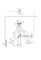
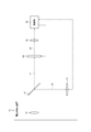
- FIG. 2 is a state diagram of an information acquisition system for explaining a traveling direction of an electromagnetic wave in a first state and a second state of a switching element in a switching unit of the electromagnetic wave detection device in FIG. 1.
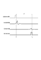
- 3 is a timing chart showing the electromagnetic wave emission timing and detection timing for explaining the principle of distance measurement by a distance measuring sensor constituted by the irradiation unit, the second detection unit, and the control unit of FIG. 1.
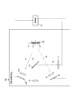
- It is a block diagram which shows schematic structure of the electromagnetic wave detection apparatus which concerns on 2nd Embodiment.
- the electromagnetic wave detection device to which the present invention is applied can reduce the difference in the coordinate system in the detection result by each detection unit by being configured to reduce the difference in detection axis in each detection unit.
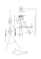
- an information acquisition system 11 including an electromagnetic wave detection device 10 according to the first embodiment of the present disclosure includes an electromagnetic wave detection device 10, an irradiation unit 12, a reflection unit 13, and a control unit 14. Has been.
- the broken lines connecting the functional blocks indicate the flow of control signals or information to be communicated.
- the communication indicated by the broken line may be wired communication or wireless communication.
- a solid line protruding from each functional block indicates a beam-like electromagnetic wave.
- the electromagnetic wave detection device 10 includes a front-stage optical system 15, a separation unit 16, a first detection unit 17, a switching unit 18, a first rear-stage optical system 19, and a second detection unit 20.
- the pre-stage optical system 15 includes, for example, at least one of a lens and a mirror, and forms an image of the object ob that is a subject.
- the separation unit 16 is provided between the front optical system 15 and a primary image formation position that is an image formation position of the object ob away from the front optical system 15 by a predetermined position. ing.
- the separation unit 16 separates the incident electromagnetic wave so as to travel in the first direction d1 and the second direction d2.
- the separation unit 16 reflects a part of the incident electromagnetic wave in the first direction d1 and transmits another part of the electromagnetic wave in the second direction d2.
- the separation unit 16 may transmit a part of the incident electromagnetic wave in the first direction d1 and transmit another part of the electromagnetic wave in the second direction d2. Further, the separating unit 16 may refract part of the incident electromagnetic wave in the first direction d1 and refract another part of the electromagnetic wave in the second direction d2.
- the separation unit 16 is, for example, a half mirror, a beam splitter, a dichroic mirror, a cold mirror, a hot mirror, a metasurface, a deflection element, and a prism.
- the first detection unit 17 is provided on the path of the electromagnetic wave that travels from the separation unit 16 in the first direction d1. Further, the first detection unit 17 captures the image of the object ob away from the front stage optical system 15 at a predetermined position by the front stage optical system 15 in the first direction d1 from the separation unit 16 or the connection position. It is provided in the vicinity of the image position. The first detection unit 17 detects the electromagnetic wave that has traveled from the separation unit 16 in the first direction d1.
- the first detection unit 17 is configured so that the first traveling axis of the electromagnetic wave traveling in the first direction d1 from the separation unit 16 is parallel to the first detection axis of the first detection unit 17.
- the separator 16 may be disposed.
- the first traveling axis is the central axis of the electromagnetic wave propagating from the separating portion 16 in the first direction d1 and propagating radially.
- the first traveling axis is an axis obtained by extending the optical axis of the front optical system 15 to the separation unit 16 and bending the separation unit 16 so as to be parallel to the first direction d1.
- the first detection axis is an axis that passes through the center of the detection surface of the first detection unit 17 and is perpendicular to the detection surface.
- the first detection unit 17 may be arranged so that the interval between the first traveling axis and the first detection axis is equal to or less than the first interval threshold. Moreover, the 1st detection part 17 may be arrange
- the first detection unit 17 is separated so that the first angle formed by the first traveling axis and the detection surface of the first detection unit 17 is equal to or less than the first angle threshold value or a predetermined angle. It may be arranged with respect to the part 16. In the first embodiment, the first detector 17 is arranged so that the first angle is 90 ° as described above.
- the first detection unit 17 is a passive sensor. In the first embodiment, more specifically, the first detection unit 17 includes an element array.
- the first detection unit 17 includes an image sensor such as an image sensor or an imaging array, captures an image of an electromagnetic wave formed on the detection surface, and generates image information corresponding to the captured object ob.
- the first detection unit 17 captures an image of visible light.
- the first detection unit 17 transmits the generated image information as a signal to the control unit 14.
- the first detection unit 17 may capture images other than visible light, such as infrared, ultraviolet, and radio wave images.
- the first detection unit 17 may include a distance measuring sensor. In this configuration, the electromagnetic wave detection device 10 can acquire image-like distance information by the first detection unit 17. Further, the first detection unit 17 may include a distance measuring sensor thermosensor or the like. In this configuration, the electromagnetic wave detection device 10 can acquire image-like temperature information by the first detection unit 17.
- the switching unit 18 is provided on the path of the electromagnetic wave that travels from the separating unit 16 in the second direction d2. Further, the switching unit 18 selects the primary imaging position of the image of the object ob away from the preceding optical system 15 at a predetermined position or the primary imaging by the preceding optical system 15 in the second direction d2 from the separating unit 16. It is provided near the position.
- the switching unit 18 is provided at the imaging position.
- the switching unit 18 has a working surface as on which electromagnetic waves that have passed through the front optical system 15 and the separating unit 16 are incident.
- the action surface as is constituted by a plurality of switching elements se arranged along a two-dimensional shape.
- the action surface as is a surface that causes an action such as reflection and transmission on the electromagnetic wave in at least one of a first state and a second state to be described later.
- the switching unit 18 can switch for each switching element se between a first state in which the electromagnetic wave incident on the working surface as is advanced in the third direction d3 and a second state in which the electromagnetic wave is advanced in the fourth direction d4. It is.
- the first state is a first reflection state in which an electromagnetic wave incident on the working surface as is reflected in the third direction d3.
- the second state is a second reflection state in which the electromagnetic wave incident on the working surface as is reflected in the fourth direction d4.
- the switching unit 18 includes a reflecting surface that reflects electromagnetic waves for each switching element se.
- the switching unit 18 switches the first reflection state and the second reflection state for each switching element se by changing the direction of the reflecting surface for each switching element se.
- the switching unit 18 includes, for example, a DMD (Digital Micro Mirror Device: digital micromirror device).
- the DMD can switch the reflecting surface to either the + 12 ° or ⁇ 12 ° inclined state with respect to the working surface as for each switching element se by driving a minute reflecting surface constituting the working surface as. is there.
- the working surface as is parallel to the plate surface of the substrate on which the minute reflecting surface of the DMD is placed.
- the switching unit 18 switches the first state and the second state for each switching element se based on the control of the control unit 14 described later. For example, as shown in FIG. 2, the switching unit 18 can simultaneously advance an electromagnetic wave incident on the switching element se1 in the third direction d3 by switching some of the switching elements se1 to the first state. By switching another part of the switching element se2 to the second state, the electromagnetic wave incident on the switching element se2 can be advanced in the fourth direction d4.
- the first second-stage optical system 19 is provided in the third direction d3 from the switching unit 18.
- the first post-stage optical system 19 includes, for example, at least one of a lens and a mirror.
- the first post-stage optical system 19 forms an image of the object ob as an electromagnetic wave whose traveling direction is switched by the switching unit 18.
- the second detection unit 20 is provided on the path of the electromagnetic wave that travels in the third direction d3 by the switching unit 18 and then travels through the first second-stage optical system 19.
- the second detection unit 20 detects an electromagnetic wave that has passed through the first post-stage optical system 19, that is, an electromagnetic wave that has traveled in the third direction d3.
- the second detection unit 20 travels in the second direction d2 from the separation unit 16 together with the switching unit 18, and the second progression of the electromagnetic wave whose traveling direction is switched in the third direction d3 by the switching unit 18.
- the axis may be arranged with respect to the separation unit 16 so as to be parallel to the second detection axis of the second detection unit 20.
- the second traveling axis is the central axis of the electromagnetic wave propagating from the switching unit 18 in the third direction d3 and propagating radially.
- the second traveling axis is an axis obtained by extending the optical axis of the front optical system 15 to the switching unit 18 and bending the switching unit 18 so as to be parallel to the third direction d3.
- the second detection axis is an axis that passes through the center of the detection surface of the second detection unit 20 and is perpendicular to the detection surface.
- the second detection unit 20 and the switching unit 18 may be arranged so that the interval between the second traveling axis and the second detection axis is equal to or less than the second interval threshold.
- the second interval threshold value may be the same value as the first interval threshold value or a different value.
- the second detection unit 20, together with the first detection unit 17 and the switching unit 18, the distance between the first travel axis and the first detection axis, and the distance between the second travel axis and the second detection axis. May be arranged to be equal to or smaller than a predetermined gap difference (for example, the diameters of the detection surfaces of the first detection unit 17 and the second detection unit 20).
- the 2nd detection part 20 may be arrange
- the second detection unit 20 is arranged so that the second traveling axis and the second detection axis coincide.
- the second detection unit 20, together with the switching unit 18, has a second angle formed between the second traveling axis and the detection surface of the second detection unit 20 that is equal to or less than a second angle threshold value or a predetermined angle. It may be arranged with respect to separation part 16 so that it may become.
- the second angle threshold may be the same value as or different from the first angle threshold.
- the second detection unit 20, together with the first detection unit 17 and the switching unit 18, makes a difference between the first angle and the second angle equal to or less than a predetermined angle difference (for example, Scheimpflug's May be arranged to meet the principle).
- the second detection unit 20 is arranged so that the second angle is 90 ° as described above.
- the second detection unit 20 is an active sensor that detects a reflected wave from the target ob of the electromagnetic wave irradiated from the irradiation unit 12 toward the target ob.
- the second detection unit 20 reflects the electromagnetic wave irradiated from the irradiation unit 12 and reflected toward the target ob by being reflected by the reflection unit 13 from the target ob. Is detected.
- the electromagnetic wave emitted from the irradiation unit 12 is at least one of infrared, visible light, ultraviolet, and radio waves, and the second detection unit 20 is different from or the same type as the first detection unit 17. Detect electromagnetic waves.
- the second detection unit 20 includes an element constituting a distance measuring sensor.
- the second detection unit 20 includes a single element such as an APD (Avalanche PhotoDiode), a PD (PhotoDiode), and a ranging image sensor.
- the second detection unit 20 may include an element array such as an APD array, a PD array, a ranging imaging array, and a ranging image sensor.
- the second detection unit 20 transmits detection information indicating that a reflected wave from the subject has been detected to the control unit 14 as a signal. More specifically, the second detection unit 20 detects an electromagnetic wave in the infrared band.
- the 2nd detection part 20 should just be able to detect electromagnetic waves in the structure which is a single element which comprises the distance sensor mentioned above, and does not need to be imaged on a detection surface. Therefore, the second detection unit 20 does not have to be provided at the secondary image formation position that is the image formation position by the first post-stage optical system 19. That is, in this configuration, the second detection unit 20 is configured so that the electromagnetic wave from all the angles of view can be incident on the detection surface, and then the first detection unit 20 proceeds in the third direction d3 by the switching unit 18. It may be disposed anywhere on the path of the electromagnetic wave traveling through the post-stage optical system 19.
- the irradiation unit 12 emits at least one of infrared rays, visible rays, ultraviolet rays, and radio waves. In the first embodiment, the irradiation unit 12 emits infrared rays. The irradiation unit 12 irradiates the radiated electromagnetic wave directly or indirectly through the reflection unit 13 toward the object ob. In 1st Embodiment, the irradiation part 12 irradiates the electromagnetic wave to radiate
- the irradiation unit 12 emits a narrow electromagnetic wave in the form of a beam, for example, 0.5 °.
- the irradiation unit 12 can emit electromagnetic waves in a pulsed manner.
- the irradiation unit 12 includes an LED (Light Emitting Diode) and an LD (Laser Diode). The irradiation unit 12 switches between emission and stop of electromagnetic waves based on the control of the control unit 14 described later.
- the reflection unit 13 changes the irradiation position of the electromagnetic wave irradiated to the object ob by reflecting the electromagnetic wave radiated from the irradiation unit 12 while changing the direction. That is, the reflection unit 13 scans the object ob with the electromagnetic wave radiated from the irradiation unit 12. Therefore, in the first embodiment, the second detection unit 20 forms a scanning distance measuring sensor in cooperation with the reflection unit 13. Note that the reflection unit 13 scans the object ob in a one-dimensional direction or a two-dimensional direction. In the first embodiment, the reflecting unit 13 scans the object ob in the two-dimensional direction.
- the reflection unit 13 is configured such that at least a part of the irradiation region of the electromagnetic wave radiated and reflected from the irradiation unit 12 is included in the electromagnetic wave detection range in the electromagnetic wave detection device 10. Therefore, at least a part of the electromagnetic wave irradiated to the object ob through the reflection unit 13 can be detected by the electromagnetic wave detection device 10.
- the reflection unit 13 includes at least a part of the irradiation region of the electromagnetic wave emitted from the irradiation unit 12 and reflected by the reflection unit 13 in the detection range of the second detection unit 20. It is configured. Therefore, in the first embodiment, at least a part of the electromagnetic wave irradiated to the object ob via the reflection unit 13 can be detected by the second detection unit 20.
- the reflection unit 13 includes, for example, a MEMS (Micro Electro Mechanical Systems) mirror, a polygon mirror, and a galvanometer mirror.
- the reflection unit 13 includes a MEMS mirror.
- the reflection unit 13 changes the direction in which the electromagnetic wave is reflected based on the control of the control unit 14 described later.
- the reflection part 13 may have angle sensors, such as an encoder, for example, and may notify the angle which an angle sensor detects to the control part 14 as direction information which reflects electromagnetic waves.
- the control unit 14 can calculate the irradiation position based on the direction information acquired from the reflection unit 13.
- the control part 14 can calculate an irradiation position based on the drive signal input in order to make the reflection part 13 change the direction which reflects electromagnetic waves.
- the control unit 14 includes one or more processors and a memory.
- the processor may include at least one of a general-purpose processor that reads a specific program and executes a specific function, and a dedicated processor specialized for a specific process.
- the dedicated processor may include an application specific integrated circuit (ASIC) (ASIC; Application Specific Integrated Circuit).
- the processor may include a programmable logic device (PLD; Programmable Logic Device).
- the PLD may include an FPGA (Field-Programmable Gate Array).
- the control unit 14 may include at least one of SoC (System-on-a-Chip) in which one or more processors cooperate, and SiP (System In a Package).
- the control unit 14 acquires information about the periphery of the electromagnetic wave detection device 10 based on the electromagnetic waves detected by the first detection unit 17 and the second detection unit 20 respectively.
- the information about the surroundings is, for example, image information, distance information, temperature information, and the like.
- the control unit 14 acquires the electromagnetic waves detected as an image by the first detection unit 17 as image information.
- the control unit 14 uses the ToF (Time-of-Flight) method to irradiate the irradiation unit 12 based on detection information detected by the second detection unit 20 as described below.
- the distance information of the irradiation position irradiated on is acquired.
- the control unit 14 causes the irradiation unit 12 to emit a pulsed electromagnetic wave by inputting the electromagnetic wave emission signal to the irradiation unit 12 (see the “electromagnetic wave emission signal” column).
- the irradiation unit 12 irradiates an electromagnetic wave based on the input electromagnetic wave radiation signal (see the “irradiation unit radiation amount” column).
- An electromagnetic wave emitted from the irradiation unit 12 and reflected from the reflection unit 13 and irradiated to an arbitrary irradiation region is reflected in the irradiation region.
- the control unit 14 switches at least a part of the switching elements se in the imaging region in the switching unit 18 by the pre-stage optical system 15 of the reflected wave of the irradiation area to the first state, and sets the other switching elements se to the second state. Switch to the state. Then, the second detection unit 20 notifies the control unit 14 of the detection information as described above when detecting the electromagnetic wave reflected in the irradiation region (see the “electromagnetic wave detection amount” column).
- the control unit 14 has, for example, a time measurement LSI (Large Scale Integrated circuit), and acquires detection information (refer to the “detection information acquisition” column) from the time T1 when the irradiation unit 12 radiates electromagnetic waves. The time ⁇ T until T2 is measured.
- the control unit 14 calculates the distance to the irradiation position by multiplying the time ⁇ T by the speed of light and dividing by 2.
- the control part 14 calculates an irradiation position based on the direction information acquired from the reflection part 13 or the drive signal which self outputs to the reflection part 13 as mentioned above.
- the control unit 14 creates image-like distance information by calculating the distance to each irradiation position while changing the irradiation position.
- the information acquisition system 11 is configured to create distance information by Direct ToF that directly measures the time until the laser beam is irradiated and returned.
- the information acquisition system 11 is not limited to such a configuration.
- the information acquisition system 11 irradiates an electromagnetic wave with a fixed period, and distance information is obtained by Flash ToF that indirectly measures the time until it returns from the phase difference between the irradiated electromagnetic wave and the returned electromagnetic wave. You may create it.
- the information acquisition system 11 may create distance information by another ToF method, for example, Phased ToF.
- the electromagnetic wave detection device 10 separates an incident electromagnetic wave so as to travel in the first direction d1 and the second direction d2, and travels in the second direction d2.
- the traveling direction of the electromagnetic wave can be switched to the third direction d3.
- the electromagnetic wave detection device 10 has the optical axis of the front optical system 15 in the first traveling axis that is the central axis of the electromagnetic wave that has traveled in the first direction d1 and in the third direction d3. It is possible to match the second traveling axis, which is the central axis of the electromagnetic wave that has traveled. Therefore, the electromagnetic wave detection device 10 can reduce the deviation of the optical axes of the first detection unit 17 and the second detection unit 20.
- the electromagnetic wave detection apparatus 10 can reduce the shift
- the electromagnetic wave detection device 10 of the first embodiment is configured so that the first travel axis is parallel to the first detection axis and the second travel axis is parallel to the second detection axis.
- the first detection unit 17, the switching unit 18, and the second detection unit 20 are arranged with respect to the separation unit 16.
- the electromagnetic wave detection device 10 can reduce the deviation between the first detection axis and the second detection axis and can homogenize the imaging state of the electromagnetic wave on the detection surface regardless of the distance from the traveling axis. . Therefore, the electromagnetic wave detection device 10 can acquire information related to the surrounding in the homogeneous imaging state without performing information processing for homogenizing the imaging state in the control unit 14.
- such a structure and effect are the same also about the electromagnetic wave detection apparatus of 2nd Embodiment mentioned later.
- the first detection unit 17 is connected to the separation unit 16 so that the interval between the first traveling axis and the first detection axis is equal to or less than the first interval threshold.
- the switching unit 18 and the second detection unit 20 are arranged with respect to the separation unit 16 so that the interval between the second traveling axis and the second detection axis is equal to or less than the second interval threshold.
- the difference between the distance between the first traveling axis and the first detection axis and the distance between the second traveling axis and the second detection axis is a predetermined distance difference.
- the first detection unit 17, the switching unit 18, and the second detection unit 20 are arranged with respect to the separation unit 16 so as to be as follows. With such a configuration, the electromagnetic wave detection device 10 can further reduce the deviation between the first detection axis and the second detection axis. In addition, such a structure and effect are the same also about the electromagnetic wave detection apparatus of 2nd Embodiment mentioned later.
- the electromagnetic wave detection device 10 of the first embodiment performs the first detection so that the first traveling axis and the first detection axis coincide with each other, and the second traveling axis and the second detection axis coincide with each other.
- the unit 17, the switching unit 18, and the second detection unit 20 are arranged with respect to the separation unit 16. With this configuration, the electromagnetic wave detection device 10 can further reduce the deviation between the first detection axis and the second detection axis. In addition, such a structure and effect are the same also about the electromagnetic wave detection apparatus of 2nd Embodiment mentioned later.
- the electromagnetic wave detection device 10 of the first exemplary embodiment is configured such that the first angle is equal to or less than the first angle threshold value or a predetermined angle, and the second angle is equal to or less than the second angle threshold value or the predetermined angle.
- the first detection unit 17, the switching unit 18, and the second detection unit 20 are arranged with respect to the separation unit 16 so that With such a configuration, the electromagnetic wave detection device 10 reduces the deviation between the first detection axis and the second detection axis, and makes the imaging state of the electromagnetic wave on the detection surface inhomogeneous according to the distance from the traveling axis. Can be reduced. Therefore, the electromagnetic wave detection device 10 can reduce the load of information processing for homogenizing the imaging state in the control unit 14. In addition, such a structure and effect are the same also about the electromagnetic wave detection apparatus of 2nd Embodiment mentioned later.
- the electromagnetic wave detection device 10 of the first exemplary embodiment includes the first detection unit 17, the switching unit 18, and the first detection unit so that the difference between the first angle and the second angle is equal to or less than a predetermined angle difference.
- Two detection units 20 are arranged with respect to the separation unit 16. With such a configuration, the electromagnetic wave detection device 10 can further reduce the deviation of the optical axes of the first detection unit 17 and the second detection unit 20. In addition, such a structure and effect are the same also about the electromagnetic wave detection apparatus of 2nd Embodiment mentioned later.
- the electromagnetic wave detection device 10 can switch a part of the switching elements se in the switching unit 18 to the first state and can switch another part of the switching elements se to the second state.
- the electromagnetic wave detection device 10 can cause the second detection unit 20 to detect information based on the electromagnetic wave for each portion of the target ob that emits the electromagnetic wave incident on each switching element se.
- such a structure and effect are the same also about the electromagnetic wave detection apparatus of 2nd Embodiment mentioned later.
- the second embodiment is different from the first embodiment in that it further includes a third detection unit.
- the second embodiment will be described below with a focus on differences from the first embodiment.
- symbol is attached
- the electromagnetic wave detection device 100 includes a front optical system 15, a separation unit 16, a first detection unit 17, a switching unit 180, a first rear optical system 19, and a second optical system.
- the second stage optical system 210, the second detection unit 20, and the third detection unit 220 are included.
- the configuration of the information acquisition system 11 according to the second embodiment other than the electromagnetic wave detection device 100 is the same as that of the first embodiment.
- the configurations and functions of the front stage optical system 15, the separation unit 16, the first detection unit 17, the first rear stage optical system 19, and the second detection unit 20 in the second embodiment are the same as those in the first embodiment. It is.
- the arrangement of the switching unit 180 in the electromagnetic wave detection device 100 is the same as that in the first embodiment. Similar to the first embodiment, the switching unit 180 has an operation surface as configured by a plurality of switching elements se arranged in a two-dimensional shape. Unlike the first embodiment, the switching unit 180 is in a first state in which the electromagnetic wave incident on the working surface as is advanced in the third direction d3 and a second state in which the electromagnetic wave is advanced in the fourth direction d4. In addition, it is possible to switch for each switching element se to the third state in which the travel proceeds in a direction other than the third direction d3 and the fourth direction d4.
- the first state is a first reflection state in which the electromagnetic wave incident on the working surface as is reflected in the third direction d3.
- the second state is a second reflection state in which the electromagnetic wave incident on the working surface as is reflected in the fourth direction d4.
- the third state is a third reflection state in which the electromagnetic wave incident on the working surface as is reflected in a direction other than the third direction d3 and the fourth direction d4.
- the switching unit 180 includes a reflecting surface that reflects electromagnetic waves for each switching element se.
- the switching unit 180 switches the first reflection state, the second reflection state, and the third reflection state for each switching element se by changing the direction of the reflecting surface for each switching element se.
- the switching unit 180 includes a DMD (Digital Micro mirror Device), for example.
- the DMD can switch the reflecting surface to either the + 12 ° or ⁇ 12 ° inclined state with respect to the working surface as for each switching element se by driving a minute reflecting surface constituting the working surface as. is there. Furthermore, the DMD can switch the reflecting surface to an inclined state of about 0 ° with respect to the working surface as for each switching element se by stopping the driving of the reflecting surface.
- the switching unit 180 switches the first state, the second state, and the third state for each switching element se based on the control of the control unit 14. For example, as illustrated in FIG. 5, the switching unit 18 simultaneously sets a part of the switching elements se1, another part of the switching elements se2, and the remaining switching elements se3 to the first state, the second state, By switching to the third state, the electromagnetic waves incident on the switching elements se1, se2, and se3 are transmitted in the third direction d3, the fourth direction d4, and directions other than the third direction d3 and the fourth direction d4. Can progress to.
- the second post-stage optical system 210 is provided from the switching unit 180 in the fourth direction d4.
- the second post-stage optical system 210 includes, for example, at least one of a lens and a mirror.
- the second post-stage optical system 210 forms an image of the object ob as an electromagnetic wave whose traveling direction is switched by the switching unit 180.
- the third detection unit 220 is provided on the path of the electromagnetic wave that travels in the fourth direction d4 by the switching unit 180 and then travels through the second post-stage optical system 210.
- the third detection unit 220 detects the electromagnetic wave that has passed through the second post-stage optical system 210, that is, the electromagnetic wave that has traveled in the fourth direction d4.
- the third detection unit 220 together with the switching unit 180, travels in the second direction d2 from the separation unit 16, and travels in the third direction by the switching unit 180 in the fourth direction d4.
- the axis may be arranged with respect to the separation unit 16 so as to be parallel to the third detection axis of the third detection unit 220.
- the third traveling axis is the central axis of the electromagnetic wave propagating from the switching unit 180 in the fourth direction d4 and propagating radially.
- the third traveling axis is an axis obtained by extending the optical axis of the front optical system 15 to the switching unit 180 and bending the switching unit 180 so as to be parallel to the fourth direction d4.
- the third detection axis is an axis that passes through the center of the detection surface of the third detection unit 220 and is perpendicular to the detection surface.
- the third detection unit 220 and the switching unit 180 may be arranged so that the interval between the third traveling axis and the third detection axis is equal to or less than the third interval threshold.
- the third interval threshold may be the same value as the first interval threshold or the second interval threshold, or a different value.
- the distance between the second detection axis and the distance between the third traveling axis and the third travel axis may be arranged so as to be equal to or less than a predetermined distance difference.
- the 3rd detection part 220 may be arrange
- the third detection unit 220 is arranged such that the third traveling axis and the third detection axis coincide.
- the third detection unit 220 together with the switching unit 180, has a third angle formed by the third traveling axis and the perpendicular of the detection surface of the third detection unit 220 equal to or less than a third angle threshold or a predetermined angle. It may be arranged with respect to separation part 16 so that. Note that the third angle threshold may be the same value as or different from the first angle threshold or the second angle threshold. In addition to the first detection unit 17, the switching unit 180, and the second detection unit 20, the third detection unit 220 has a predetermined difference between the first angle, the second angle, and the third angle. It may be arranged so as to be less than the angle difference. In the second embodiment, the third detection unit 220 is arranged so that the third angle is 90 ° as described above.
- the third detection unit 220 is an active sensor that detects a reflected wave from the target ob of the electromagnetic wave irradiated from the irradiation unit 12 toward the target ob.
- the third detection unit 220 reflects the electromagnetic wave irradiated from the irradiation unit 12 and reflected toward the target ob by being reflected by the reflection unit 13 from the target ob. Is detected.
- the electromagnetic wave irradiated from the irradiation unit 12 is at least one of infrared rays, visible light, ultraviolet rays, and radio waves, and the third detection unit 220 is different from or the same type as the first detection unit 17.
- the second detection unit 20 detects the same type of electromagnetic waves.
- the third detection unit 220 includes elements constituting a distance measuring sensor.
- the third detection unit 220 includes an APD (Avalanche PhotoDiode), a PD (PhotoDiode), a SPAD (Single Photo Avalanche Diode), an MPPC (Multi-Pixel Photo Counter), and a ranging image sensor.
- the third detection unit 220 may include an element array such as a SPAD array, an APD array, a PD array, a ranging imaging array, and a ranging image sensor.
- the third detection unit 220 transmits detection information indicating that a reflected wave from the subject has been detected to the control unit 14 as a signal. More specifically, the third detection unit 220 detects electromagnetic waves in the infrared band.
- the 3rd detection part 220 should just be able to detect electromagnetic waves in the structure which is a single element which comprises the distance sensor mentioned above, and does not need to be imaged on a detection surface. Therefore, the third detection unit 220 may not be provided at the secondary image formation position that is the image formation position by the second second-stage optical system 210. That is, in this configuration, the third detection unit 220 is configured so that the electromagnetic wave from all angles of view can enter the detection surface, and then the second detection unit 220 proceeds to the fourth direction d4 by the switching unit 180. It may be disposed anywhere on the path of the electromagnetic wave traveling through the post-stage optical system 210.
- control unit 14 differs from the first embodiment in that at least a part of the switching elements se in the imaging region in the switching unit 180 by the pre-stage optical system 15 of the reflected wave in the electromagnetic wave irradiation region. Is switched to the first state, another part of the switching elements se in the imaging region is switched to the second state, and the remaining switching elements se are switched to the third state.
- the electromagnetic wave detection device 100 includes the third detection unit 220 that detects the electromagnetic wave that has traveled from the switching unit 180 in the fourth direction d4.
- the electromagnetic wave detection device 100 travels in the third direction d3 with the optical axis of the front optical system 15 as the first travel axis that is the central axis of the electromagnetic wave traveled in the first direction d1. It is possible to match the second traveling axis, which is the central axis of the electromagnetic wave, and the third traveling axis, which is the central axis of the electromagnetic wave advanced in the fourth direction d4. Therefore, the electromagnetic wave detection device 100 can reduce the deviation of the optical axes of the first detection unit 17, the second detection unit 20, and the third detection unit 220.
- the electromagnetic wave detection apparatus 100 can reduce the deviation of the first detection axis, the second detection axis, and the third detection axis. Therefore, the electromagnetic wave detection device 100 can reduce the shift of the coordinate system in the detection results by the first detection unit 17, the second detection unit 20, and the third detection unit 220.
- the electromagnetic wave detection device 100 can switch a part of the switching elements se in the switching unit 180 to the first state and can switch another part of the switching elements se to the second state.
- the electromagnetic wave detection device 100 causes the electromagnetic wave to travel toward the second detection unit 20 in a part of the switching elements se and simultaneously uses the third detection unit 220 in another part of the switching elements se. Electromagnetic waves can be advanced toward Therefore, the electromagnetic wave detection device 100 can simultaneously acquire information regarding different regions.
- the electromagnetic wave detection apparatus 100 can shorten the time required for acquiring image-like distance information, for example.
- the third detection unit 220 is connected to the separation unit 16 together with the switching unit 180 so that the third traveling axis is parallel to the third detection axis. Has been placed.
- the electromagnetic wave detection device 100 reduces the deviation of the first detection axis, the second detection axis, and the third detection axis, and the third detection axis regardless of the distance from the third traveling axis.
- the imaging state of the electromagnetic wave on the detection surface of the detection unit 220 can be homogenized. Therefore, the electromagnetic wave detection device 100 can acquire information related to the surrounding in the homogeneous imaging state without performing information processing for homogenizing the imaging state in the control unit 14.
- the third detection unit 220 includes the switching unit 180 so that the interval between the third traveling axis and the third detection axis is equal to or less than the third interval threshold. In addition, it is arranged with respect to the separation part 16. With such a configuration, the electromagnetic wave detection device 100 can further reduce the deviation of the third detection axis with respect to the first detection axis or the second detection axis.
- the electromagnetic wave detection device 100 includes the distance between the third traveling axis and the third detection axis, the distance between the first traveling axis and the first detection axis, the second traveling axis, and the second traveling axis.
- the first detection unit 17, the switching unit 180, the second detection unit 20, and the third detection unit 220 are separated by the separation unit 16 so that the difference between the two detection axis intervals is equal to or less than a predetermined interval difference. Is arranged against.
- the electromagnetic wave detection device 100 can further reduce the deviation of the third detection axis with respect to the first detection axis and the second detection axis.
- the third detection unit 220 is connected to the separation unit 16 together with the switching unit 180 so that the third traveling axis and the third detection axis coincide with each other. Has been placed.
- the electromagnetic wave detection device 100 can further reduce the deviation of the third detection axis with respect to the first detection axis and the second detection axis.
- the third detection unit 220 and the switching unit 180 together with the separation unit 16 so that the third angle is equal to or smaller than the third angle threshold value or a predetermined angle. Is arranged against.
- the electromagnetic wave detection device 100 reduces the deviation of the first detection axis, the second detection axis, and the third detection axis, and the third according to the distance from the third traveling axis. This can reduce the heterogeneity of the imaging state of the electromagnetic wave on the detection surface of the detection unit 220. Therefore, the electromagnetic wave detection device 100 can reduce the load of information processing for homogenizing the imaging state in the control unit 14.
- the electromagnetic wave detection device 100 is configured so that the first detection unit 17 is switched so that the difference between the third angle, the first angle, and the second angle is equal to or less than a predetermined angle difference.
- the unit 180, the second detection unit 20, and the third detection unit 220 are arranged with respect to the separation unit 16. With such a configuration, the electromagnetic wave detection device 100 can further reduce the deviation of the optical axis of the third detection unit 220 with respect to the first detection unit 17 and the second detection unit 20.
- the irradiation unit 12, the reflection unit 13, and the control unit 14 constitute the information acquisition system 11 together with the electromagnetic wave detection devices 10 and 100.
- 10, 100 may be configured to include at least one of these.
- the switching unit 18 can switch the traveling direction of the electromagnetic wave incident on the working surface as to two directions. However, the switching unit 18 does not switch to one of the two directions, but to three or more directions. It may be switchable. In the second embodiment, the switching unit 180 can switch the traveling direction of the electromagnetic wave incident on the working surface as in three directions, but may switch in four or more directions.
- the first state and the second state are the first reflection state in which the electromagnetic wave incident on the working surface as is reflected in the third direction d3, respectively. Although it is the 2nd reflective state which reflects in the 4th direction d4, other modes may be sufficient.
- the first state may be a transmission state in which the electromagnetic wave incident on the working surface as is transmitted and travels in the third direction d3.
- the switching unit 181 may include a shutter having a reflection surface that reflects the electromagnetic wave in the fourth direction for each switching element.
- the transmission state as the first state and the reflection state as the second state can be switched for each switching element by opening and closing the shutter for each switching element.
- Examples of the switching unit 181 having such a configuration include a switching unit including a MEMS shutter in which a plurality of shutters that can be opened and closed are arranged in an array.
- the switching unit 181 includes a switching unit including a liquid crystal shutter that can switch between a reflection state that reflects electromagnetic waves and a transmission state that transmits electromagnetic waves in accordance with the liquid crystal alignment.
- the transmission state as the first state and the reflection state as the second state can be switched for each switching element by switching the liquid crystal alignment for each switching element.
- the information acquisition system 11 causes the second detection unit 20 to cooperate with the reflection unit 13 by causing the reflection unit 13 to scan a beam-like electromagnetic wave emitted from the irradiation unit 12. It has a structure that functions as a scanning type active sensor. Further, in the second embodiment, the information acquisition system 11 causes the second detection unit 20 and the third detection unit 220 to scan by causing the reflection unit 13 to scan the beam-shaped electromagnetic wave radiated from the irradiation unit 12. It has a configuration that functions as a scanning type active sensor in cooperation with the reflection unit 13. However, the information acquisition system 11 is not limited to such a configuration. For example, even if the information acquisition system 11 does not include the reflection unit 13 and radiates a radial electromagnetic wave from the irradiation unit 12 and acquires information without scanning, an effect similar to that of the first embodiment can be obtained.
- the information acquisition system 11 has a configuration in which the first detection unit 17 is a passive sensor and the second detection unit 20 is an active sensor.
- the information acquisition system 11 is not limited to such a configuration.
- the information acquisition system 11 an effect similar to that of the first embodiment can be obtained regardless of whether the first detection unit 17 and the second detection unit 20 are both active sensors or passive sensors.
- the information acquisition system 11 has a configuration in which the first detection unit 17 is a passive sensor and the second detection unit 20 and the third detection unit 220 are active sensors.
- the information acquisition system 11 is not limited to such a configuration.
- the first detection unit 17, the second detection unit 20, and the third detection unit 220 are both active sensors or passive sensors. Similar effects are obtained.
- the configuration in which any two of the first detection unit 17, the second detection unit 20, and the third detection unit 220 are passive sensors is similar to the second embodiment. An effect is obtained.
Landscapes
- Engineering & Computer Science (AREA)
- Physics & Mathematics (AREA)
- General Physics & Mathematics (AREA)
- Radar, Positioning & Navigation (AREA)
- Remote Sensing (AREA)
- Computer Networks & Wireless Communication (AREA)
- Electromagnetism (AREA)
- Optics & Photonics (AREA)
- Optical Radar Systems And Details Thereof (AREA)
- Geophysics And Detection Of Objects (AREA)
- Light Receiving Elements (AREA)
Abstract
Description
入射する電磁波を第1の方向および第2の方向に進行するように分離する分離部と、
前記第1の方向に進行した前記電磁波を検出する第1の検出部と、
前記第2の方向に進行した電磁波の進行方向を、第3の方向および第4の方向に切替え可能な複数の切替素子を有する切替部と、
前記第3の方向に進行した前記電磁波を検出する第2の検出部と、を備える。
入射する電磁波を第1の方向および第2の方向に進行するように分離する分離部と、前記第1の方向に進行した前記電磁波を検出する第1の検出部と、前記第2の方向に進行した電磁波の進行方向を第3の方向および第4の方向に切替え可能な複数の切替素子を有する切替部と、前記第3の方向に進行した前記電磁波を検出する第2の検出部と、を有する電磁波検出装置と、
前記第1の検出部および前記第2の検出部による電磁波の検出結果に基づいて、前記電磁波検出装置の周囲に関する情報を取得する制御部と、を備える。
11 情報取得システム
12 照射部
13 反射部
14 制御部
15 前段光学系
16 分離部
17 第1の検出部
18、180、181 切替部
19 第1の後段光学系
20 第2の検出部
210 第2の後段光学系
220 第3の検出部
as 作用面
d1、d2、d3、d4 第1の方向、第2の方向、第3の方向、第4の方向
ob 対象
Claims (31)
- 入射する電磁波を第1の方向および第2の方向に進行するように分離する分離部と、
前記第1の方向に進行した前記電磁波を検出する第1の検出部と、
前記第2の方向に進行した電磁波の進行方向を、第3の方向および第4の方向に切替え
可能な複数の切替素子を有する切替部と、
前記第3の方向に進行した前記電磁波を検出する第2の検出部と、を備える
電磁波検出装置。 - 請求項1に記載の電磁波検出装置において、
前記第1の検出部は、前記分離部から前記第1の方向に進行する前記電磁波の中心軸である第1の進行軸が、前記第1の検出部による電磁波の検出面の中心を通り前記検出面に垂直な第1の検出軸と平行となるように配置され、
前記切替部および前記第2の検出部は、前記分離部から前記第2の方向に進行して前記切替部により前記第3の方向に進行方向が切替えられた前記電磁波の中心軸である第2の進行軸が、前記第2の検出部による電磁波の検出面の中心を通り前記検出面に垂直な第2の検出軸と平行となるように配置されている
電磁波検出装置。 - 請求項2に記載の電磁波検出装置において、
前記第1の検出部は、前記第1の進行軸および前記第1の検出軸の間隔が第1の間隔閾値以下となるように配置され、
前記切替部および前記第2の検出部は、前記第2の進行軸および前記第2の検出軸の間隔が第2の間隔閾値以下となるように配置されている
電磁波検出装置。 - 請求項2または3に記載の電磁波検出装置において、
前記第1の検出部、前記切替部、および前記第2の検出部は、前記第1の進行軸および前記第1の検出軸の間隔と、前記第2の進行軸および前記第2の検出軸の間隔との差が所定の間隔差以下なるように配置されている
電磁波検出装置。 - 請求項2から4のいずれか1項に記載の電磁波検出装置において、
前記第1の検出部は、前記第1の進行軸および前記第1の検出軸が一致するように配置され、
前記切替部および第2の検出部は、前記第2の進行軸および前記第2の検出軸が一致するように配置されている
電磁波検出装置。 - 請求項1から5のいずれか1項に記載の電磁波検出装置において、
前記第1の検出部は、前記分離部から前記第1の方向に進行する前記電磁波の中心軸と、前記第1の検出部の検出面とのなす第1の角度が第1の角度閾値以下または所定の角度となるように配置され、
前記切替部および前記第2の検出部は、前記分離部から前記第2の方向に進行して前記切替部により前記第3の方向に進行方向が切替えられた前記電磁波の中心軸と、前記第2の検出部の検出面とのなす第2の角度が第2の角度閾値以下または所定の角度となるように配置されている
電磁波検出装置。 - 請求項6に記載の電磁波検出装置において、
前記第1の検出部、前記切替部、および前記第2の検出部は、前記第1の角度と前記第2の角度との差が所定の角度差以下となるように配置されている
電磁波検出装置。 - 請求項1から7のいずれか1項に記載の電磁波検出装置において、
前記第4の方向に進行した前記電磁波を検出する第3の検出部を、さらに備える
電磁波検出装置。 - 請求項8に記載の電磁波検出装置において、
前記切替部および前記第3の検出部は、前記分離部により前記第2の方向に進行して前記切替部により前記第4の方向に進行方向が切替えられた前記電磁波の中心軸である第3の進行軸が、前記第3の検出部による電磁波の検出面の中心を通り前記検出面に垂直な第3の検出軸と平行となるように配置されている
電磁波検出装置。 - 請求項9に記載の電磁波検出装置において、
前記切替部および前記第3の検出部は、前記第3の進行軸および前記第3の検出軸の間隔が第3の間隔閾値以下となるように配置されている
電磁波検出装置。 - 請求項4に記載の電磁波検出装置において、
前記第4の方向に進行した前記電磁波を検出する第3の検出部を、さらに備え、
前記切替部および前記第3の検出部は、前記分離部により前記第2の方向に進行して前記切替部により前記第4の方向に進行方向が切替えられた前記電磁波の中心軸である第3の進行軸、および前記第3の検出部による電磁波の検出面の中心を通り前記検出面に垂直な第3の検出軸の間隔と、前記第1の進行軸および前記第1の検出軸の間隔、ならびに前記第2の進行軸および前記第2の検出軸の間隔との差が前記所定の間隔差となるように、配置されている
電磁波検出装置。 - 請求項9から11のいずれか1項に記載の電磁波検出装置において、
前記切替部および第3の検出部は、前記第3の進行軸および前記第3の検出軸が一致するように配置されている
電磁波検出装置。 - 請求項8から12のいずれか1項に記載の電磁波検出装置において、
前記切替部および前記第3の検出部は、前記分離部により前記第2の方向に進行して前記切替部により前記第4の方向に進行方向が切替えられた前記電磁波の中心軸と、前記第2の検出部による電磁波の検出面とのなす第3の角度が第3の角度閾値以下または所定の角度となるように配置されている
電磁波検出装置。 - 請求項6に記載の電磁波検出装置において、
前記第4の方向に進行した前記電磁波を検出する第3の検出部を、さらに備え、
前記前記切替部および前記第3の検出部は、前記分離部により前記第2の方向に進行して前記切替部により前記第4の方向に進行方向が切替えられた前記電磁波の中心軸と、前記第2の検出部による電磁波の検出面とのなす第3の角度と、前記第1の角度および前記第2の角度との差が所定の角度差以下となるように配置されている
電磁波検出装置。 - 請求項1から14のいずれか1項に記載の電磁波検出装置において、
前記分離部は、入射する電磁波の一部を前記第1の方向に反射し、該電磁波の別の一部を前記第2の方向に透過する
電磁波検出装置。 - 請求項1から14のいずれか1項に記載の電磁波検出装置において、
前記分離部は、入射する電磁波の一部を前記第1の方向に透過し、該電磁波の別の一部を前記第2の方向に透過する
電磁波検出装置。 - 請求項1から14のいずれか1項に記載の電磁波検出装置において、
前記分離部は、入射する電磁波の一部を前記第1の方向に屈折させ、該電磁波の別の一部を前記第2の方向に屈折させる
電磁波検出装置。 - 請求項1から17のいずれか1項に記載の電磁波検出装置において、
前記分離部は、ハーフミラー、ビームスプリッタ、ダイクロイックミラー、コールドミラー、ホットミラー、およびメタサーフェスの少なくともいずれかを含む
電磁波検出装置。 - 請求項1から18のいずれか1項に記載の電磁波検出装置において、
前記切替部は、前記第2の方向に進行した電磁波を、前記第3の方向に反射する第1の反射状態と、前記第4の方向に反射する第2の反射状態とに、前記切替素子毎に切替える
電磁波検出装置。 - 請求項19に記載の電磁波検出装置において、
前記切替素子は電磁波を反射する反射面を有し、
前記切替部は、前記切替素子毎に、前記反射面の向きを変更することにより前記第1の反射状態と前記第2の反射状態とを、切替える
電磁波検出装置。 - 請求項19または20に記載の電磁波検出装置において、
前記切替部は、デジタルマイクロミラーデバイスを含む
電磁波検出装置。 - 請求項1から18のいずれか1項に記載の電磁波検出装置において、
前記切替部は、前記第2の方向に進行した電磁波を、前記第3の方向に透過する透過状態と、前記第4の方向に反射させる反射状態とに、前記切替素子毎に切替える
電磁波検出装置。 - 請求項22に記載の電磁波検出装置において、
前記切替素子は電磁波を反射する反射面を含むシャッタを有し、
前記切替素子毎に、前記シャッタを開閉することにより前記反射状態と前記透過状態とを、切替る
電磁波検出装置。 - 請求項22または23に記載の電磁波検出装置において、
前記切替部は、開閉可能な複数の前記シャッタがアレイ状に配列されたMEMSシャッ
タを含む
電磁波検出装置。 - 請求項22に記載の電磁波検出装置において、
前記切替部は、電磁波を反射する反射状態および透過する透過状態を液晶配光に応じて
前記切替素子毎に切替可能な液晶シャッタを含む
電磁波検出装置。 - 請求項1から25のいずれか1項に記載の電磁波検出装置において、
前記第1の検出部および前記第2の検出部はそれぞれ、測距センサ、イメージセンサ、およびサーモセンサの少なくともいずれかを含む
電磁波検出装置。 - 請求項1から26のいずれか1項に記載の電磁波検出装置において、
前記第1の検出部および前記第2の検出部による電磁波の検出結果に基づいて、周囲に関する情報を取得する制御部を、さらに備える
電磁波検出装置。 - 請求項27に記載の電磁波検出装置において、
前記制御部は、前記周囲に関する情報として、画像情報、距離情報、および温度情報の少なくともいずれかを取得する
電磁波検出装置。 - 請求項1から28のいずれか1項に記載の電磁波検出装置において、
前記第1の検出部および前記第2の検出部は、異種または同種の電磁波を検出する
電磁波検出装置。 - 請求項1から29のいずれか1項に記載の電磁波検出装置において、
前記第1の検出部および前記第2の検出部はそれぞれ、赤外線、可視光線、紫外線、および電波の少なくともいずれかを検出する
電磁波検出装置。 - 入射する電磁波を第1の方向および第2の方向に進行するように分離する分離部と、前記第1の方向に進行した前記電磁波を検出する第1の検出部と、前記第2の方向に進行した電磁波の進行方向を第3の方向および第4の方向に切替え可能な複数の切替素子を有する切替部と、前記第3の方向に進行した前記電磁波を検出する第2の検出部と、を有する電磁波検出装置と、
前記第1の検出部および前記第2の検出部による電磁波の検出結果に基づいて、前記電磁波検出装置の周囲に関する情報を取得する制御部と、を備える
情報取得システム。
Priority Applications (11)
| Application Number | Priority Date | Filing Date | Title |
|---|---|---|---|
| EP18805062.9A EP3633735A4 (en) | 2017-05-25 | 2018-05-16 | ELECTROMAGNETIC WAVE DETECTION DEVICE, PROGRAM, AND INFORMATION ACQUISITION SYSTEM |
| CN201880034041.9A CN110678773A (zh) | 2017-05-25 | 2018-05-16 | 电磁波检测装置以及信息获取系统 |
| CN202310796522.6A CN116840810A (zh) | 2017-05-25 | 2018-05-16 | 电磁波检测装置以及信息获取系统 |
| US16/615,102 US10838044B2 (en) | 2017-05-25 | 2018-05-16 | Electromagnetic wave detection apparatus and information acquisition system |
| CN202310802084.XA CN116840814A (zh) | 2017-05-25 | 2018-05-16 | 电磁波检测装置以及信息获取系统 |
| CN202310798046.1A CN116840811A (zh) | 2017-05-25 | 2018-05-16 | 电磁波检测装置以及信息获取系统 |
| KR1020217039383A KR102456631B1 (ko) | 2017-05-25 | 2018-05-16 | 전자파 검출 장치 및 정보 취득 시스템 |
| KR1020197034525A KR102335830B1 (ko) | 2017-05-25 | 2018-05-16 | 전자파 검출 장치 및 정보 취득 시스템 |
| CN202310799028.5A CN116840812A (zh) | 2017-05-25 | 2018-05-16 | 电磁波检测装置以及信息获取系统 |
| US17/027,371 US11719790B2 (en) | 2017-05-25 | 2020-09-21 | Electromagnetic wave detection apparatus and information acquisition system |
| US18/336,372 US12313783B2 (en) | 2017-05-25 | 2023-06-16 | Electromagnetic wave detection apparatus and information acquisition system |
Applications Claiming Priority (2)
| Application Number | Priority Date | Filing Date | Title |
|---|---|---|---|
| JP2017-103942 | 2017-05-25 | ||
| JP2017103942A JP6640149B2 (ja) | 2017-05-25 | 2017-05-25 | 電磁波検出装置および情報取得システム |
Related Child Applications (2)
| Application Number | Title | Priority Date | Filing Date |
|---|---|---|---|
| US16/615,102 A-371-Of-International US10838044B2 (en) | 2017-05-25 | 2018-05-16 | Electromagnetic wave detection apparatus and information acquisition system |
| US17/027,371 Division US11719790B2 (en) | 2017-05-25 | 2020-09-21 | Electromagnetic wave detection apparatus and information acquisition system |
Publications (1)
| Publication Number | Publication Date |
|---|---|
| WO2018216573A1 true WO2018216573A1 (ja) | 2018-11-29 |
Family
ID=64396420
Family Applications (1)
| Application Number | Title | Priority Date | Filing Date |
|---|---|---|---|
| PCT/JP2018/018954 Ceased WO2018216573A1 (ja) | 2017-05-25 | 2018-05-16 | 電磁波検出装置および情報取得システム |
Country Status (6)
| Country | Link |
|---|---|
| US (3) | US10838044B2 (ja) |
| EP (1) | EP3633735A4 (ja) |
| JP (1) | JP6640149B2 (ja) |
| KR (2) | KR102335830B1 (ja) |
| CN (5) | CN110678773A (ja) |
| WO (1) | WO2018216573A1 (ja) |
Cited By (1)
| Publication number | Priority date | Publication date | Assignee | Title |
|---|---|---|---|---|
| WO2022186225A1 (ja) * | 2021-03-02 | 2022-09-09 | 京セラ株式会社 | 電磁波検出装置及び移動体 |
Families Citing this family (19)
| Publication number | Priority date | Publication date | Assignee | Title |
|---|---|---|---|---|
| CN111316138B (zh) | 2017-05-24 | 2022-05-17 | 纽约市哥伦比亚大学理事会 | 色散工程化介电超表面的宽带消色差平坦光学部件 |
| JP6640149B2 (ja) * | 2017-05-25 | 2020-02-05 | 京セラ株式会社 | 電磁波検出装置および情報取得システム |
| JP7461294B2 (ja) | 2017-08-31 | 2024-04-03 | メタレンズ,インコーポレイテッド | 透過型メタサーフェスレンズ統合 |
| CN118295056A (zh) | 2018-01-24 | 2024-07-05 | 哈佛学院院长及董事 | 利用超表面的偏振状态生成 |
| JP7091131B2 (ja) * | 2018-05-08 | 2022-06-27 | 京セラ株式会社 | 電磁波検出装置及び情報取得システム |
| SG11202013228XA (en) | 2018-07-02 | 2021-01-28 | Metalenz Inc | Metasurfaces for laser speckle reduction |
| JP7004632B2 (ja) * | 2018-10-05 | 2022-01-21 | 京セラ株式会社 | 電磁波検出装置 |
| EP4004608A4 (en) | 2019-07-26 | 2023-08-30 | Metalenz, Inc. | APERTURE METASURFACE AND HYBRID REFRACTIVE METASURFACE IMAGING SYSTEMS |
| US11578968B1 (en) | 2019-10-31 | 2023-02-14 | President And Fellows Of Harvard College | Compact metalens depth sensors |
| JP7194709B2 (ja) * | 2020-04-03 | 2022-12-22 | 京セラ株式会社 | 測距装置 |
| JP7372205B2 (ja) | 2020-05-21 | 2023-10-31 | 京セラ株式会社 | 電磁波検出装置および測距装置 |
| JP7535394B2 (ja) | 2020-07-01 | 2024-08-16 | 京セラ株式会社 | 画像処理装置および測距装置 |
| JP7523970B2 (ja) * | 2020-07-01 | 2024-07-29 | 京セラ株式会社 | 測定装置及び測定方法 |
| JP7402129B2 (ja) * | 2020-07-01 | 2023-12-20 | 京セラ株式会社 | 電磁波検出装置、測距装置および電磁波検出方法 |
| JP7603431B2 (ja) | 2020-12-08 | 2024-12-20 | 京セラ株式会社 | 電磁波検出装置及び電磁波検出方法 |
| EP4348780A4 (en) | 2021-05-25 | 2025-04-23 | Metalenz, Inc. | Single element dot pattern projector |
| DE102021130334A1 (de) * | 2021-11-19 | 2023-05-25 | Sick Ag | Optoelektronischer Sensor |
| CN120188073A (zh) | 2022-03-31 | 2025-06-20 | 梅特兰兹股份有限公司 | 偏振分选超颖表面微透镜阵列设备 |
| CN115327678B (zh) * | 2022-09-01 | 2024-11-22 | 天津山河光电科技有限公司 | 双向光路系统、光学模组及光学设备 |
Citations (7)
| Publication number | Priority date | Publication date | Assignee | Title |
|---|---|---|---|---|
| JPH0587584U (ja) * | 1992-04-27 | 1993-11-26 | 三菱電機株式会社 | 捜索監視装置 |
| JP2004014802A (ja) * | 2002-06-06 | 2004-01-15 | Sony Corp | 撮像装置 |
| JP2004163271A (ja) * | 2002-11-13 | 2004-06-10 | Tokyo Denki Univ | 非接触画像計測装置 |
| JP2008128792A (ja) * | 2006-11-20 | 2008-06-05 | Fujifilm Corp | 距離画像作成装置及び方法 |
| JP2011220732A (ja) | 2010-04-06 | 2011-11-04 | Honda Motor Co Ltd | 車両の周辺監視装置 |
| JP2014512525A (ja) * | 2011-03-17 | 2014-05-22 | ウニベルジテート ポリテクニカ デ カタル−ニア | 光ビームを受光するシステムと方法とコンピュータ・プログラム |
| US20150378023A1 (en) * | 2013-02-13 | 2015-12-31 | Universitat Politecnica De Catalunya | System and method for scanning a surface and computer program implementing the method |
Family Cites Families (23)
| Publication number | Priority date | Publication date | Assignee | Title |
|---|---|---|---|---|
| JPH0743115A (ja) | 1993-07-26 | 1995-02-10 | Sony Corp | 距離測定方法および距離測定装置 |
| JP2001311612A (ja) | 2000-04-28 | 2001-11-09 | Minolta Co Ltd | 形状入力装置 |
| JP3766326B2 (ja) | 2001-12-10 | 2006-04-12 | 日本電信電話株式会社 | 光照射受光装置 |
| JP2004157044A (ja) * | 2002-11-07 | 2004-06-03 | Nippon Signal Co Ltd:The | 走査型レーザレーダ |
| CN1702452B (zh) | 2004-05-24 | 2011-05-04 | 中国科学院光电技术研究所 | 数字微镜多目标成像光谱仪装置 |
| DE102005049471B4 (de) * | 2005-10-13 | 2007-09-13 | Ingenieurbüro Spies GbR (vertretungsberechtigte Gesellschafter: Hans Spies, Martin Spies, 86558 Hohenwart) | Entfernungssensor mit Einzelflächenabtastung |
| US7483151B2 (en) * | 2006-03-17 | 2009-01-27 | Alpineon D.O.O. | Active 3D triangulation-based imaging method and device |
| CN101568962A (zh) * | 2006-12-29 | 2009-10-28 | 松下电器产业株式会社 | 光学拾波器、光盘装置、复合耦合透镜、复合棱镜及光学信息设备 |
| JP2010096574A (ja) | 2008-10-15 | 2010-04-30 | Ihi Corp | レーザレーダ及びレーザレーダによる計測方法 |
| JP5821333B2 (ja) * | 2011-06-30 | 2015-11-24 | セイコーエプソン株式会社 | 光学式位置検出装置および入力機能付き表示システム |
| US8506209B2 (en) * | 2011-07-26 | 2013-08-13 | Iscar, Ltd. | Adjustable cutting tool |
| CN102426027B (zh) * | 2011-09-05 | 2013-10-02 | 南京德朔实业有限公司 | 激光测距仪内光路控制切换装置 |
| WO2013053952A1 (en) * | 2011-10-14 | 2013-04-18 | Iee International Electronics & Engineering S.A. | Spatially selective detection using a dynamic mask in an image plane |
| EP2708913A1 (de) | 2012-09-18 | 2014-03-19 | Sick Ag | Optoelektronischer Sensor und Verfahren zur Objekterfassung |
| AU2014310703B2 (en) * | 2013-08-19 | 2018-09-27 | Basf Se | Optical detector |
| EP2860550B1 (de) * | 2013-10-09 | 2016-03-02 | Hexagon Technology Center GmbH | Scanner zur Raumvermessung |
| CN106464858B (zh) * | 2014-04-26 | 2019-08-20 | 泰特拉维公司 | 用于3d成像中的深度感测的耐用且延伸的照明波形的方法和系统 |
| WO2016157593A1 (ja) * | 2015-03-27 | 2016-10-06 | 富士フイルム株式会社 | 距離画像取得装置及び距離画像取得方法 |
| US9766081B2 (en) * | 2015-05-12 | 2017-09-19 | Here Global B.V. | System and method for roundabouts from probe data using vector fields |
| EP3165876A3 (de) * | 2015-11-03 | 2017-07-26 | Hexagon Technology Center GmbH | Opto-elektronisches vermessungsgerät |
| US20170357000A1 (en) | 2016-06-09 | 2017-12-14 | Texas Instruments Incorporated | Processing techniques for lidar receiver using spatial light modulators |
| KR101825994B1 (ko) * | 2016-06-24 | 2018-02-06 | (주)에이앤아이 | 직선편광으로 인한 계측오차가 보정된 휘도색도계 |
| JP6640149B2 (ja) * | 2017-05-25 | 2020-02-05 | 京セラ株式会社 | 電磁波検出装置および情報取得システム |
-
2017
- 2017-05-25 JP JP2017103942A patent/JP6640149B2/ja active Active
-
2018
- 2018-05-16 CN CN201880034041.9A patent/CN110678773A/zh active Pending
- 2018-05-16 CN CN202310798046.1A patent/CN116840811A/zh active Pending
- 2018-05-16 KR KR1020197034525A patent/KR102335830B1/ko active Active
- 2018-05-16 KR KR1020217039383A patent/KR102456631B1/ko active Active
- 2018-05-16 EP EP18805062.9A patent/EP3633735A4/en active Pending
- 2018-05-16 CN CN202310799028.5A patent/CN116840812A/zh active Pending
- 2018-05-16 WO PCT/JP2018/018954 patent/WO2018216573A1/ja not_active Ceased
- 2018-05-16 US US16/615,102 patent/US10838044B2/en active Active
- 2018-05-16 CN CN202310802084.XA patent/CN116840814A/zh active Pending
- 2018-05-16 CN CN202310796522.6A patent/CN116840810A/zh active Pending
-
2020
- 2020-09-21 US US17/027,371 patent/US11719790B2/en active Active
-
2023
- 2023-06-16 US US18/336,372 patent/US12313783B2/en active Active
Patent Citations (7)
| Publication number | Priority date | Publication date | Assignee | Title |
|---|---|---|---|---|
| JPH0587584U (ja) * | 1992-04-27 | 1993-11-26 | 三菱電機株式会社 | 捜索監視装置 |
| JP2004014802A (ja) * | 2002-06-06 | 2004-01-15 | Sony Corp | 撮像装置 |
| JP2004163271A (ja) * | 2002-11-13 | 2004-06-10 | Tokyo Denki Univ | 非接触画像計測装置 |
| JP2008128792A (ja) * | 2006-11-20 | 2008-06-05 | Fujifilm Corp | 距離画像作成装置及び方法 |
| JP2011220732A (ja) | 2010-04-06 | 2011-11-04 | Honda Motor Co Ltd | 車両の周辺監視装置 |
| JP2014512525A (ja) * | 2011-03-17 | 2014-05-22 | ウニベルジテート ポリテクニカ デ カタル−ニア | 光ビームを受光するシステムと方法とコンピュータ・プログラム |
| US20150378023A1 (en) * | 2013-02-13 | 2015-12-31 | Universitat Politecnica De Catalunya | System and method for scanning a surface and computer program implementing the method |
Cited By (3)
| Publication number | Priority date | Publication date | Assignee | Title |
|---|---|---|---|---|
| WO2022186225A1 (ja) * | 2021-03-02 | 2022-09-09 | 京セラ株式会社 | 電磁波検出装置及び移動体 |
| JP2022133958A (ja) * | 2021-03-02 | 2022-09-14 | 京セラ株式会社 | 電磁波検出装置及び移動体 |
| JP7723485B2 (ja) | 2021-03-02 | 2025-08-14 | 京セラ株式会社 | 電磁波検出装置及び移動体 |
Also Published As
| Publication number | Publication date |
|---|---|
| CN116840812A (zh) | 2023-10-03 |
| US12313783B2 (en) | 2025-05-27 |
| JP6640149B2 (ja) | 2020-02-05 |
| US20200174101A1 (en) | 2020-06-04 |
| US10838044B2 (en) | 2020-11-17 |
| EP3633735A4 (en) | 2020-12-09 |
| JP2018200927A (ja) | 2018-12-20 |
| CN116840810A (zh) | 2023-10-03 |
| CN116840814A (zh) | 2023-10-03 |
| US20230333214A1 (en) | 2023-10-19 |
| CN110678773A (zh) | 2020-01-10 |
| KR20200003840A (ko) | 2020-01-10 |
| KR102456631B1 (ko) | 2022-10-18 |
| KR102335830B1 (ko) | 2021-12-07 |
| US11719790B2 (en) | 2023-08-08 |
| CN116840811A (zh) | 2023-10-03 |
| US20210003673A1 (en) | 2021-01-07 |
| EP3633735A1 (en) | 2020-04-08 |
| KR20210149244A (ko) | 2021-12-08 |
Similar Documents
| Publication | Publication Date | Title |
|---|---|---|
| KR102456631B1 (ko) | 전자파 검출 장치 및 정보 취득 시스템 | |
| JP7387803B2 (ja) | 電磁波検出装置および情報取得システム | |
| US11675052B2 (en) | Electromagnetic wave detection apparatus, program, and electromagnetic wave detection system | |
| US11573316B2 (en) | Electromagnetic wave detection apparatus and information acquisition system | |
| WO2019220978A1 (ja) | 電磁波検出装置および情報取得システム | |
| WO2020105419A1 (ja) | 電磁波検出装置および情報取得システム | |
| WO2019159933A1 (ja) | 電磁波検出装置および情報取得システム | |
| JP2019144219A (ja) | 電磁波検出装置および情報取得システム | |
| JP2022173534A (ja) | 電磁波検出装置および情報取得システム | |
| JP2020073895A (ja) | 電磁波検出装置および情報取得システム | |
| WO2019220974A1 (ja) | 電磁波検出装置および情報取得システム | |
| JP2019002847A (ja) | 電磁波検出装置および情報取得システム |
Legal Events
| Date | Code | Title | Description |
|---|---|---|---|
| 121 | Ep: the epo has been informed by wipo that ep was designated in this application |
Ref document number: 18805062 Country of ref document: EP Kind code of ref document: A1 |
|
| ENP | Entry into the national phase |
Ref document number: 20197034525 Country of ref document: KR Kind code of ref document: A |
|
| NENP | Non-entry into the national phase |
Ref country code: DE |
|
| WWE | Wipo information: entry into national phase |
Ref document number: 2018805062 Country of ref document: EP |
|
| ENP | Entry into the national phase |
Ref document number: 2018805062 Country of ref document: EP Effective date: 20200102 |