WO2018221060A1 - 測距センサ - Google Patents
測距センサ Download PDFInfo
- Publication number
- WO2018221060A1 WO2018221060A1 PCT/JP2018/016178 JP2018016178W WO2018221060A1 WO 2018221060 A1 WO2018221060 A1 WO 2018221060A1 JP 2018016178 W JP2018016178 W JP 2018016178W WO 2018221060 A1 WO2018221060 A1 WO 2018221060A1
- Authority
- WO
- WIPO (PCT)
- Prior art keywords
- light
- substrate
- distance measuring
- measuring sensor
- light source
- Prior art date
- Legal status (The legal status is an assumption and is not a legal conclusion. Google has not performed a legal analysis and makes no representation as to the accuracy of the status listed.)
- Ceased
Links
Images




Classifications
-
- G—PHYSICS
- G01—MEASURING; TESTING
- G01S—RADIO DIRECTION-FINDING; RADIO NAVIGATION; DETERMINING DISTANCE OR VELOCITY BY USE OF RADIO WAVES; LOCATING OR PRESENCE-DETECTING BY USE OF THE REFLECTION OR RERADIATION OF RADIO WAVES; ANALOGOUS ARRANGEMENTS USING OTHER WAVES
- G01S17/00—Systems using the reflection or reradiation of electromagnetic waves other than radio waves, e.g. lidar systems
- G01S17/02—Systems using the reflection of electromagnetic waves other than radio waves
- G01S17/06—Systems determining position data of a target
- G01S17/08—Systems determining position data of a target for measuring distance only
- G01S17/32—Systems determining position data of a target for measuring distance only using transmission of continuous waves, whether amplitude-, frequency-, or phase-modulated, or unmodulated
-
- G—PHYSICS
- G01—MEASURING; TESTING
- G01S—RADIO DIRECTION-FINDING; RADIO NAVIGATION; DETERMINING DISTANCE OR VELOCITY BY USE OF RADIO WAVES; LOCATING OR PRESENCE-DETECTING BY USE OF THE REFLECTION OR RERADIATION OF RADIO WAVES; ANALOGOUS ARRANGEMENTS USING OTHER WAVES
- G01S7/00—Details of systems according to groups G01S13/00, G01S15/00, G01S17/00
- G01S7/48—Details of systems according to groups G01S13/00, G01S15/00, G01S17/00 of systems according to group G01S17/00
- G01S7/481—Constructional features, e.g. arrangements of optical elements
- G01S7/4817—Constructional features, e.g. arrangements of optical elements relating to scanning
-
- G—PHYSICS
- G01—MEASURING; TESTING
- G01S—RADIO DIRECTION-FINDING; RADIO NAVIGATION; DETERMINING DISTANCE OR VELOCITY BY USE OF RADIO WAVES; LOCATING OR PRESENCE-DETECTING BY USE OF THE REFLECTION OR RERADIATION OF RADIO WAVES; ANALOGOUS ARRANGEMENTS USING OTHER WAVES
- G01S17/00—Systems using the reflection or reradiation of electromagnetic waves other than radio waves, e.g. lidar systems
- G01S17/02—Systems using the reflection of electromagnetic waves other than radio waves
- G01S17/06—Systems determining position data of a target
- G01S17/08—Systems determining position data of a target for measuring distance only
- G01S17/32—Systems determining position data of a target for measuring distance only using transmission of continuous waves, whether amplitude-, frequency-, or phase-modulated, or unmodulated
- G01S17/34—Systems determining position data of a target for measuring distance only using transmission of continuous waves, whether amplitude-, frequency-, or phase-modulated, or unmodulated using transmission of continuous, frequency-modulated waves while heterodyning the received signal, or a signal derived therefrom, with a locally-generated signal related to the contemporaneously transmitted signal
-
- G—PHYSICS
- G01—MEASURING; TESTING
- G01S—RADIO DIRECTION-FINDING; RADIO NAVIGATION; DETERMINING DISTANCE OR VELOCITY BY USE OF RADIO WAVES; LOCATING OR PRESENCE-DETECTING BY USE OF THE REFLECTION OR RERADIATION OF RADIO WAVES; ANALOGOUS ARRANGEMENTS USING OTHER WAVES
- G01S17/00—Systems using the reflection or reradiation of electromagnetic waves other than radio waves, e.g. lidar systems
- G01S17/88—Lidar systems specially adapted for specific applications
- G01S17/93—Lidar systems specially adapted for specific applications for anti-collision purposes
- G01S17/931—Lidar systems specially adapted for specific applications for anti-collision purposes of land vehicles
-
- G—PHYSICS
- G01—MEASURING; TESTING
- G01S—RADIO DIRECTION-FINDING; RADIO NAVIGATION; DETERMINING DISTANCE OR VELOCITY BY USE OF RADIO WAVES; LOCATING OR PRESENCE-DETECTING BY USE OF THE REFLECTION OR RERADIATION OF RADIO WAVES; ANALOGOUS ARRANGEMENTS USING OTHER WAVES
- G01S7/00—Details of systems according to groups G01S13/00, G01S15/00, G01S17/00
- G01S7/003—Transmission of data between radar, sonar or lidar systems and remote stations
- G01S7/006—Transmission of data between radar, sonar or lidar systems and remote stations using shared front-end circuitry, e.g. antennas
-
- G—PHYSICS
- G01—MEASURING; TESTING
- G01S—RADIO DIRECTION-FINDING; RADIO NAVIGATION; DETERMINING DISTANCE OR VELOCITY BY USE OF RADIO WAVES; LOCATING OR PRESENCE-DETECTING BY USE OF THE REFLECTION OR RERADIATION OF RADIO WAVES; ANALOGOUS ARRANGEMENTS USING OTHER WAVES
- G01S7/00—Details of systems according to groups G01S13/00, G01S15/00, G01S17/00
- G01S7/48—Details of systems according to groups G01S13/00, G01S15/00, G01S17/00 of systems according to group G01S17/00
- G01S7/481—Constructional features, e.g. arrangements of optical elements
- G01S7/4811—Constructional features, e.g. arrangements of optical elements common to transmitter and receiver
-
- G—PHYSICS
- G01—MEASURING; TESTING
- G01S—RADIO DIRECTION-FINDING; RADIO NAVIGATION; DETERMINING DISTANCE OR VELOCITY BY USE OF RADIO WAVES; LOCATING OR PRESENCE-DETECTING BY USE OF THE REFLECTION OR RERADIATION OF RADIO WAVES; ANALOGOUS ARRANGEMENTS USING OTHER WAVES
- G01S7/00—Details of systems according to groups G01S13/00, G01S15/00, G01S17/00
- G01S7/48—Details of systems according to groups G01S13/00, G01S15/00, G01S17/00 of systems according to group G01S17/00
- G01S7/481—Constructional features, e.g. arrangements of optical elements
- G01S7/4811—Constructional features, e.g. arrangements of optical elements common to transmitter and receiver
- G01S7/4813—Housing arrangements
-
- G—PHYSICS
- G02—OPTICS
- G02F—OPTICAL DEVICES OR ARRANGEMENTS FOR THE CONTROL OF LIGHT BY MODIFICATION OF THE OPTICAL PROPERTIES OF THE MEDIA OF THE ELEMENTS INVOLVED THEREIN; NON-LINEAR OPTICS; FREQUENCY-CHANGING OF LIGHT; OPTICAL LOGIC ELEMENTS; OPTICAL ANALOGUE/DIGITAL CONVERTERS
- G02F1/00—Devices or arrangements for the control of the intensity, colour, phase, polarisation or direction of light arriving from an independent light source, e.g. switching, gating or modulating; Non-linear optics
- G02F1/29—Devices or arrangements for the control of the intensity, colour, phase, polarisation or direction of light arriving from an independent light source, e.g. switching, gating or modulating; Non-linear optics for the control of the position or the direction of light beams, i.e. deflection
- G02F1/31—Digital deflection, i.e. optical switching
- G02F1/313—Digital deflection, i.e. optical switching in an optical waveguide structure
Definitions
- the present disclosure relates to a distance measuring sensor.
- LIDAR Light Detection and Ranging
- a TOF Time of Flight
- the TOF type LIDAR needs to be enlarged in order to detect a long distance of 100 m or more required for in-vehicle use due to the principle of measurement. Is not suitable.
- the FMCW (Frequency-Modulated-Continuous-Wave) LIDAR which calculates the distance to the object by heterodyne detection that synthesizes the transmitted light and the received light and examines these frequency differences, is different from the TOF LIDAR. It can be made smaller.
- Non-Patent Document 1 proposes a LIDAR in which components such as a light source, a scanning unit, a light receiver, and a processing circuit are integrated in one semiconductor chip by silicon photonics technology.
- a LIDAR can be made smaller in size than a LIDAR in which the above-described components are configured separately.
- the manufacturing cost can be reduced.
- the FMCW LIDAR since the FMCW LIDAR has high sensitivity, it can detect the long distance required for the in-vehicle LIDAR.
- in-vehicle LIDAR is required to have a wider angle in addition to long-distance detection. For example, when measuring the distance to an object included in each of a plurality of regions arranged in the horizontal direction and the vertical direction, a total of 30000 points are required, 1500 points in the horizontal direction and 20 points in the vertical direction. .
- the time required for heterodyne detection is normally 10 to 100 ⁇ sec, and the number of measurements per cycle is 500 to 5000, especially at a frame rate of 20 Hz, that is, a 50 msec cycle required for in-vehicle use. Can not meet the demands of. Therefore, a distance measuring sensor capable of operating at a higher frame rate than before is required.
- the light source that generates light and the light receiver that receives the reflected light of the light generated by the light source are formed on the same substrate. Measurement using a heterodyne detection that uses the light generated by the light source and the light applied to the light receiver to detect the distance from an object contained in a predetermined area in one direction and the other direction in the external space.
- a distance sensor that scans light generated by a light source in a direction corresponding to one direction, a diffusing lens that diffuses light generated by the light source in a direction corresponding to another direction, and a light source
- a plurality of multiplexers that combine the received light and the light applied to the light receiver to form an optical signal
- a processing unit that calculates a distance from the object based on the optical signal formed by the multiplexer,
- the receiver is arranged in a direction corresponding to the other direction.
- An optical antenna is provided, and a multiplexer is connected to each of the plurality of light receiving antennas, and the processing unit calculates the distance from the object based on the optical signal formed by the multiplexer in parallel for each of the plurality of light receiving antennas.
- the plurality of light receiving antennas are arranged in a direction corresponding to the direction in which the light is diffused, and the light from the light source and the light irradiated to the light receiving antenna are combined, and the distance to the object is calculated.
- Each of the plurality of light receiving antennas is processed in parallel. Therefore, it is possible to measure the distance to an object existing in the external space at a time for a wide area in the external space, and it is possible to operate at a high frame rate.
- FIG. 16 is a cross-sectional view taken along the line XVI-XVI in FIG. 15. It is a top view of the distance measuring sensor concerning 8th Embodiment. It is a top view of the distance measuring sensor concerning 9th Embodiment. It is sectional drawing of the ranging sensor concerning other embodiment. It is sectional drawing of the ranging sensor concerning other embodiment.
- the distance measuring sensor according to the present embodiment is used as, for example, a vehicle-mounted LIDAR, and irradiates light to a region included in a predetermined range in two directions that are perpendicular to each other outside the vehicle. Detect distance etc.
- the distance measuring sensor includes an LD (laser diode) 1, a modulator 2, an amplifier 3, a duplexer 4, a scanning unit 5, a light receiver 6, a multiplexer 7, and a converter. 8, a TIA (transimpedance amplifier) 9, and a calculation unit 10.
- LD laser diode
- modulator 2 an amplifier
- duplexer 4 a scanning unit 5
- light receiver 6 a multiplexer 7
- a converter a multiplexer 7
- a converter a duplexer 4
- a scanning unit 5 a light receiver 6
- a multiplexer 7 a converter
- a converter a multiplexer 7
- a converter a converter
- 8 a TIA (transimpedance amplifier) 9
- a calculation unit 10 are formed on the substrate 11 by silicon photonics, and constitute an optical integrated chip.
- the substrate 11 further includes an optical waveguide 12 that transmits an optical signal and a wiring 13 that transmits an electrical signal.
- the optical waveguide 12 corresponds
- the substrate 11 includes a support layer 11a made of a Si, a sacrificial layer 11b made of a SiO 2, Si SOI configuration has been active layer 11c are sequentially stacked in (Silicon on Insulator) substrate It is.
- the surface of the substrate 11 has a square shape with a side of 10 mm, for example.
- the active layer 11c is partially removed by etching, and the active layer 11c and the sacrificial layer 11b exposed by removing the active layer 11c are covered with an insulating film 14 made of SiO 2 .
- the optical waveguide 12 is configured with the active layer 11c as a core layer and the sacrificial layer 11b covering the active layer 11c and the insulating film 14 as a cladding layer.
- the wiring 13 is composed of a layer of Al or the like formed on the surface of the insulating film 14.
- the core layer of the optical waveguide 12 is made of Si, and the cladding layer is made of SiO 2.
- these layers may be made of other materials.
- the core layer of the optical waveguide 12 is made of at least one material selected from Si or SiO 2 , SiN, SiON, LN (LiNbO 3 ), or InP doped with impurities.
- the cladding layer is made of at least one material selected from SiO 2 , SiN, SiON, LN, and InGaAsP.
- the core layer and the cladding layer have different material configurations.
- the refractive index of the core layer is higher than that of the cladding layer. In such a configuration, an optical signal is efficiently transmitted by the optical waveguide 12, and the SNR (Signal Noise Ratio) of the distance measuring sensor is improved.
- the distance measuring sensor is an optical package including a mirror 15, a case 16, a lid 17, a diffusion lens 18, and a condenser lens 19.
- the case 16 is a rectangular parallelepiped frame having an opening on one side and a space formed therein, and is made of ceramic or the like.
- the substrate 11 and the mirror 15 are disposed inside the case 16.
- the opening of the case 16 is closed by a lid 17, and a diffusing lens 18 and a condensing lens 19 are disposed outside the lid 17.
- the LD 1 generates light for irradiating the outside and corresponds to a light source.
- the LD 1 is a DFB (Distributed FeedBack) type laser diode, and is mounted on the substrate 11 by flip chip or the like.
- the LD 1 includes an active layer 1a made of a III-V group semiconductor, a p-type cladding layer 1b and an n-type cladding disposed on both sides of the active layer 1a. Layer 1c.
- the LD 1 includes an n-type substrate 1d, and an n-type cladding layer 1c, an active layer 1a, and a p-type cladding layer 1b are sequentially formed on one surface of the n-type substrate 1d. As shown in FIG. 4, in part of the substrate 11, the insulating film 14, the active layer 11c, and part of the sacrificial layer 11b are removed, and the LD 1 forms a p-type on the remaining sacrificial layer 11b. It arrange
- the p-type cladding layer 1b, the active layer 1a, the n-type cladding layer 1c, and the n-type substrate 1d are sequentially stacked on the sacrificial layer 11b. Since the LD 1 is composed of a III-V group semiconductor, the output is increased.
- the wavelength of light generated by the LD 1 is 0.85 ⁇ m or more and 0.95 ⁇ m or less, or 1.5 ⁇ m or more and 1.6 ⁇ m or less.
- the LD 1 is connected to the modulator 2 by the optical waveguide 12, and the optical signal generated by the LD 1 is input to the modulator 2.
- a gap is formed between the LD 1 and the optical waveguide 12, and the light generated by the LD 1 enters the optical waveguide 12 beyond this gap.
- the modulator 2 modulates the frequency of the light generated by the LD 1.
- the modulator 2 for example, an SSB (Single Side Band) modulator or the like is used.
- the frequency of the light generated by the LD 1 is changed by the modulator 2 as shown in FIG. That is, the frequency repeatedly increases and decreases with the passage of time, and a graph showing the relationship between time and frequency becomes a triangular wave.
- the solid line indicates the frequency of the optical signal output from the modulator 2
- the alternate long and short dash line indicates the frequency of the optical signal input from the light receiver 6 to the multiplexer 7.
- the modulator 2 is connected to the duplexer 4 via the amplifier 3 by the optical waveguide 12, and the optical signal whose frequency is modulated by the modulator 2 is amplified by the amplifier 3. Thereafter, the signal is input to the duplexer 4.
- the duplexer 4 is composed of a coupler from which the optical waveguide 12 is branched. A part of the optical signal input to the duplexer 4 is input to the scanning unit 5 and the other part is input to the multiplexer 7. Entered. A portion of the optical waveguide 12 that connects the duplexer 4 and the scanning unit 5 is an optical waveguide 12a, and a portion that connects the duplexer 4 and the multiplexer 7 is an optical waveguide 12b.
- the distance measuring sensor irradiates light to a region included in a predetermined range in two directions perpendicular to each other outside the vehicle, and detects a distance from an object outside the vehicle. Specifically, the distance measuring sensor divides a predetermined area of the space outside the vehicle into a plurality of areas in the horizontal direction and in a direction perpendicular to the horizontal plane, and the distance to the object included in each of the divided areas Is calculated.
- the horizontal direction and the direction perpendicular to the horizontal plane are defined as an H direction and a V direction, respectively.
- a plurality of multiplexers 7 are arranged according to the resolution in the V direction of the distance measuring sensor, that is, the number of divisions in the V direction of the predetermined area.
- the optical signal input to the demultiplexer 4 is divided and input to a plurality of multiplexers 7 via the optical waveguide 12b.
- the resolution of the distance measuring sensor is 1500 in the H direction and 20 in the V direction.
- 20 multiplexers 7 are arranged, and the optical waveguide 12 is branched into one optical waveguide 12 a and 20 optical waveguides 12 b in the duplexer 4.
- the scanning unit 5 scans the input optical signal in the H direction.
- the scanning unit 5 of the present embodiment is configured by OPA (Optical Phased Array). Specifically, as shown in FIG. 1, the optical waveguide 12a is branched in the scanning unit 5. If the branched optical waveguide 12 is an optical waveguide 12c, a phase shifter 20 is disposed in each optical waveguide 12c. Has been. Each optical waveguide 12 c is formed so as to reach the side surface of the substrate 11, and light is emitted from the optical waveguide 12 c exposed on the side surface of the substrate 11 to the outside of the substrate 11. The optical waveguide 12c corresponds to a scanning optical waveguide.
- OPA Optical Phased Array
- the optical waveguide 12a of this embodiment is branched into the optical waveguide 12c corresponding to the resolution in the H direction of the distance measuring sensor, and the same number of phase shifters 20 are arranged as the optical waveguide 12c.
- the phase shifter 20 changes the phase of the optical signal input from the duplexer 4 in accordance with an electrical signal input from a control circuit (not shown).
- the phase of the optical signal passing through each optical waveguide 12c is periodically changed by each phase shifter 20, whereby the phase of the light emitted from each optical waveguide 12c is periodically changed.
- the directivity of the light emitted from the entirety of the plurality of optical waveguides 12c changes, and the light is scanned in the H direction.
- the substrate 11 and the mirror 15 are arranged inside the case 16 so that the light emitted from the side surface of the substrate 11 is irradiated to the mirror 15.
- the light emitted from the substrate 11 is reflected by the mirror 15 and applied to the lid 17.
- the lid 17 is made of glass or the like that transmits light emitted from the substrate 11, and the light applied to the lid 17 passes through the lid 17 and is applied to the diffusion lens 18.
- the mirror 15 travels in the direction of light emitted from the substrate 11 so that the travel direction of the light applied to the diffusion lens 18 is parallel to the travel direction of the light applied from the condenser lens 19 to the light receiver 6. Is equivalent to a direction adjusting mirror.
- the mirror 15 is disposed so as to adjust the traveling direction of the light applied to the diffusion lens 18 in a direction perpendicular to the surface of the substrate 11.
- the direction perpendicular to the surface of the substrate 11 includes not only a direction completely perpendicular to the surface of the substrate 11 but also a substantially perpendicular direction.
- the direction parallel to the surface of the substrate 11 includes not only a direction completely parallel to the surface of the substrate 11 but also a substantially parallel direction.
- the diffusing lens 18 diffuses irradiated light to form a line beam, and is composed of a cylindrical lens or the like.
- the diffusion lens 18 of the present embodiment is disposed on the surface of the lid 17 so as to diffuse the irradiated light in the V direction.
- the light diffused by the diffusing lens 18 is irradiated outside the distance measuring sensor. Then, the light reflected by the external object is applied to the condenser lens 19.
- the condenser lens 19 is disposed on the surface of the lid 17.
- the condensing lens 19 condenses the reflected light of the light emitted from the diffusing lens 18 to the outside of the distance measuring sensor and irradiates the light receiver 6, and has a convex shape toward the opposite side of the lid 17. Has been.
- the traveling direction of the light applied to the light receiver 6 is made perpendicular to the surface of the substrate 11 by the condenser lens 19.
- the light applied to the condenser lens 19 from the outside of the distance measuring sensor is applied to the light receiver 6 through the lid 17.
- the light receiver 6 includes a plurality of light receiving antennas 21 arranged in the V direction, and light passing through the lid 17 is irradiated to each light receiving antenna 21. Twenty light receiving antennas 21 are arranged corresponding to the resolution in the V direction of the distance measuring sensor.
- the light receiving antenna 21 is constituted by a diffraction grating as shown in FIG. In FIG. 6, illustration of the insulating film 14 is omitted.
- This diffraction grating is composed of a fan-shaped active layer 11c extending on both sides of an axis parallel to the H direction, and a plurality of slits along the fan-shaped circumference are formed in the fan-shaped active layer 11c.
- a BPF (band pass filter) 22 and a polarizing filter 23 are laminated on the light receiving antenna 21.
- the BPF 22 allows light in a predetermined frequency band to pass and blocks light in other frequency bands.
- the BPF 22 is configured by alternately laminating a TiO 2 film 24 having a high refractive index and a SiO 2 film 25 having a low refractive index, and both the lowermost layer and the uppermost layer are formed as a TiO 2 film 24.
- the polarizing filter 23 passes light polarized in a predetermined direction and blocks light polarized in other directions.
- the polarizing filter 23 includes an SiO 2 film 26 laminated on the BPF 22 and an Al wire grid 27 laminated on the SiO 2 film 26.
- the BPF 22 and the polarization filter 23 remove unnecessary noise component light, and the light receiving antenna 21 is irradiated with light in a predetermined frequency band polarized in a predetermined direction.
- the light receiving antenna 21 is connected to the multiplexer 7 by the optical waveguide 12, and the optical signal output from the light receiving antenna 21 is input to the multiplexer 7.
- the light receiving antenna 21 of the present embodiment has a width in the H direction larger than a width in the V direction. Therefore, since reflected light can be received in a wide range in the H direction, the SNR of the distance measuring sensor is improved.
- the multiplexer 7 generates a waveform by multiplexing the optical signal input from the duplexer 4 and the optical signal input from the light receiving antenna 21, and corresponds to the resolution in the V direction of the distance measuring sensor. Are arranged.
- the optical signals from the duplexer 4 and the light receiving antennas 21 are input to each multiplexer 7.
- Each multiplexer 7 outputs an optical signal formed by multiplexing two input optical signals.
- the multiplexer 7 is connected to the converter 8 by the optical waveguide 12, and the optical signal formed by the multiplexer 7 is input to the converter 8.
- the converter 8 converts the input optical signal into an electric signal.
- the converter 8 of the present embodiment is composed of a PIN photodiode, and outputs a current signal according to the input optical signal.
- the converter 8 may be composed of an avalanche photodiode.
- the distance measuring sensor can be obtained by using the converter 8 as a photodiode made of Si semiconductor. SNR can be improved. Further, when the wavelength of light generated by the LD 1 is 1.5 ⁇ m or more and 1.6 ⁇ m or less, the SNR of the distance measuring sensor can be improved by making the converter 8 a photodiode made of a Ge semiconductor. Can do.
- a plurality of converters 8 are arranged corresponding to the resolution in the V direction of the distance measuring sensor in the same manner as the multiplexer 7. An optical signal is input.
- the converter 8 is connected to the TIA 9 by a wiring 13.
- a plurality of TIAs 9 are arranged on the substrate 11 similarly to the converters 8, and current signals output from the converters 8 are input to the TIAs 9.
- the TIA 9 converts the current signal input from the converter 8 into a voltage signal and outputs the voltage signal.
- the TIA 9 is connected to the calculation unit 10 by the wiring 13, and the voltage signal output from the TIA 9 is input to the calculation unit 10.
- a plurality of such light receiving antennas 21, multiplexers 7, converters 8, and TIAs 9 can be formed on the substrate 11 by using a batch process of semiconductor technology.
- the calculation unit 10 processes the input electrical signal and calculates the distance to the object by heterodyne detection.
- the converter 8, the TIA 9, and the calculation unit 10 correspond to a processing unit.
- the ADC 28 converts the electrical signal output from the TIA 9 into a digital signal and outputs the digital signal.
- the FFT circuit 29 detects a frequency component included in the digital signal output from the ADC 28.
- the imaging processing circuit 30 calculates the distance to the object and the speed of the object based on the frequency component detected by the FFT circuit 29, and forms two-dimensional data. Data formed by the imaging processing circuit 30 is transmitted to an ECU (not shown) mounted on the vehicle and used for automatic braking or the like for avoiding a collision with an object.
- the LD 1, the modulator 2, the converter 8, the TIA 9, the calculation unit 10, and the phase shifter 20 are connected to an external control circuit by a wiring (not shown), and according to an electric signal input from the control circuit. Operate.
- the distance measuring sensor of this embodiment detects the distance to the object and the speed of the object by the FMCW method using the coherence of the laser light.
- an optical signal is input from the LD 1 to the modulator 2.
- the modulator 2 periodically increases or decreases the frequency of the input optical signal to form a triangular wave as shown by the solid line in FIG.
- the modulator 2 forms a triangular wave having a period T in which the frequency is repeatedly increased and decreased between f 0 ⁇ f / 2 and f 0 + ⁇ f / 2 with f 0 as the center.
- the optical signal formed by the modulator 2 is amplified by the amplifier 3 and then input to the scanning unit 5 and the multiplexer 7 via the duplexer 4.
- the scanning unit 5 periodically changes the phase of the input optical signal by the phase shifter 20. Thereby, the directivity of the light emitted from the side surface of the substrate 11 to the outside of the substrate 11 periodically changes, and the light is scanned in the H direction.
- the light emitted from the side surface of the substrate 11 to the outside of the substrate 11 is reflected by the mirror 15, and the traveling direction is set to a direction perpendicular to the surface of the substrate 11, and the lid 17 and the diffusion lens 18 are irradiated.
- the light applied to the diffusion lens 18 is diffused in the V direction and applied to the outside of the vehicle. At this time, since the light is diffused in the V direction, it is possible to irradiate the light in a wide range in the V direction at a time as shown in FIG.
- the i-th region in the H direction and the j-th region in the V direction are defined as regions Ri, j .
- light can be irradiated onto the regions R 1, 1 to R 1, n at a time.
- the scanning unit 5 scans the light in the H direction, so that the regions R i, 1 to R i, n can be irradiated with light at a time.
- the regions R i, 1 to R i, 20 can be irradiated with light.
- the light irradiated to the outside of the vehicle is reflected by an object outside the vehicle, irradiated to the condensing lens 19, and irradiated to the light receiving antenna 21 through the condensing lens 19, the lid 17, the polarizing filter 23, and the BPF 22.
- the plurality of light receiving antennas 21 are arranged in the V direction, the light reflected by the objects included in the plurality of regions arranged in the V direction can be received at a time.
- the reflected light from the objects included in the regions R 1,1 to R 1, n is irradiated to the region R1 in FIG.
- the region R2 is irradiated.
- the plurality of light receiving antennas 21 are respectively irradiated with reflected light from objects included in the regions R i, 1 to R i, n .
- the light applied to the light receiving antenna 21 is input to the multiplexer 7 and is combined with the optical signal input from the duplexer 4 to the multiplexer 7.
- the optical signal formed by combining the two optical signals by the multiplexer 7 is converted into a current signal by the converter 8, further converted into a voltage signal by the TIA 9, and input to the calculation unit 10.
- Each multiplexer 7, each converter 8, and each TIA 9 simultaneously performs optical signal processing and the like for each light receiving antenna 21. That is, the plurality of multiplexers 7 combine the reflected light from the regions R i, 1 to R i, n and the optical signal input from the demultiplexer 4 simultaneously for each region.
- a plurality of converters 8 and a plurality of TIAs 9 simultaneously convert the optical signals formed by the multiplexer 7 into electrical signals for each region.
- the signal input to the calculation unit 10 is converted into a digital signal by the ADC 28 and input to the FFT circuit 29.
- the FFT circuit 29 detects the frequency component of the input signal, and the imaging processing circuit 30 calculates the distance to the object and the speed of the object based on the detected frequency component.
- One beat frequency f B1 is the difference in frequency when the two light frequencies are both increasing
- the other beat frequency f B2 is the frequency difference when the two light frequencies are both decreasing. It is a difference.
- the calculation of the distance to the object and the speed of the object is performed each time the scanning unit 5 scans light in the H direction. That is, when the regions R i, 1 to R i, n are irradiated with light and the distances from the objects included in the regions R i, 1 to R i, n are calculated, the scanning unit 5 moves the light in the traveling direction. To change. As a result, the region irradiated with light changes as indicated by an arrow A1 in FIG. Then, the areas R i + 1, 1 to R i + 1, n are irradiated with light , and the distances from the objects included in the areas R i + 1,1 to R i + 1, n are calculated.
- the conventional distance measuring sensor irradiates light to one of the regions surrounded by a broken line, that is, the regions R 1, 1 to R m, n , as indicated by arrows A 2, A 3.
- the light was scanned in both the H direction and the V direction, and the distance from the object included in each region was calculated in order.
- the light emitted from the substrate 11 is diffused in the V direction by the diffusing lens 18, the light can be irradiated to a wide range in the V direction at a time.
- a plurality of light receiving antennas 21 are arranged in the V direction, and a multiplexer 7, a converter 8, and a TIA 9 are arranged corresponding to each light receiving antenna 21. For this reason, reflected light from a wide range in the V direction can be received at once, and signals from the respective light receiving antennas 21 can be processed in parallel to calculate the distance to the object and the like.
- the distance to an object included in a predetermined area can be calculated, and two-dimensional data can be formed.
- the ranging sensor can be used by being mounted on a vehicle or the like that moves at high speed.
- scanning control is easier than in the case where the light is scanned in both the H direction and the V direction.
- the optical waveguide 12 is formed so as to reach the side surface of the substrate 11, light can be emitted from the side surface of the substrate 11 with high efficiency. Thereby, the SNR of the distance measuring sensor is improved.
- the light is emitted from the side surface of the substrate 11. Either the reflected light or the reflected light from the object must be reflected by the mirror.
- the outgoing light is reflected by the mirror 15 so that the traveling direction of the outgoing light is perpendicular to the surface of the substrate 11.
- the light receiving antenna 21 formed on the surface of the substrate 11 is irradiated with the reflected light from the object, and the distance measuring sensor can be used as the LIDAR.
- the light receiving antenna 21 since the light receiving antenna 21 has a long shape in the H direction, the SNR is improved, and long distance detection of, for example, 100 m or more required for in-vehicle use can be performed.
- the distance measuring sensor can be downsized as compared with the case where the scanning unit 5 is arranged outside the substrate 11.
- the distance measuring sensor can be downsized as compared with the case where these filters are arranged separately from the substrate 11. .
- the distance measuring sensor of this embodiment includes a substrate 31 that is different from the substrate 11.
- the calculation unit 10 is formed on the substrate 31.
- substrate 31 may be arrange
- the substrate 11 and the substrate 31 are respectively formed with a pad 32 and a pad 33 made of a conductive material, and the pad 32 and the pad 33 are connected by a bonding wire 34.
- the TIA 9 formed on the substrate 11 and the calculation unit 10 formed on the substrate 31 are connected by a pad 32, a pad 33, and a bonding wire 34.
- the components formed on the substrate 11 are an optical circuit unit in which information is transmitted by an optical signal through the optical waveguide 12, and an electric circuit unit in which information is transmitted by an electric signal through the wiring 13. And divided. If the process rule of the optical circuit unit determined by the minimum line width of the optical waveguide 12 is greatly different from the process rule of the electric circuit unit including the wiring 13, the manufacturing cost of the distance measuring sensor increases due to the difference of the process rule. There is.
- the calculation unit 10 which is a part of the electric circuit unit on the substrate 31 different from the substrate 11 on which the optical circuit unit is formed, an increase in manufacturing cost due to a difference in process rules can be suppressed. it can. Moreover, even when there is a difference in yield between the optical circuit portion and the electric circuit portion, an increase in manufacturing cost can be suppressed by forming them on separate substrates.
- a light source that generates light to be radiated to the outside includes an SOA (semiconductor optical amplifier) 35 and a resonator 36.
- SOA semiconductor optical amplifier
- the SOA 35 includes an active layer 35a made of a III-V group semiconductor, and a p-type cladding layer 35b and an n-type cladding layer 35c arranged on both sides of the active layer 35a. These layers are laminated on the substrate 11 by flip chip or the like in the order of the p-type cladding layer 35b, the active layer 35a, and the n-type cladding layer 35c. Since the SOA 35 is composed of a III-V group semiconductor, the output is increased.
- the resonator 36 for example, a double ring resonator or the like is used.
- a part of the optical waveguide 12 connecting the resonator 36 and the modulator 2 constitutes a coupler, and the light generated by the light source composed of the SOA 35 and the resonator 36 is transmitted to the modulator 2 via this coupler.
- a coupler A part of the optical waveguide 12 connecting the resonator 36 and the modulator 2 constitutes a coupler, and the light generated by the light source composed of the SOA 35 and the resonator 36 is transmitted to the modulator 2 via this coupler.
- FIG. 11 shows an example in which a directional coupler is used as a coupler, a multimode interference (MMI) coupler may be used.
- MMI multimode interference
- the laser length generated by the LD 1 configured by the DFB laser is set so that the line width of the laser light generated by the SOA 35 is increased by increasing the resonator length of the resonator 36. It is possible to make it narrower than the line width of light. Therefore, the detection accuracy of the distance to the object can be improved.
- the scanning unit 5 of the present embodiment includes a plurality of optical switches 37.
- the optical switch 37 is disposed in each optical waveguide 12 c and includes a micro heater 38.
- the micro heater 38 changes the temperature band of the optical waveguide 12c and changes the frequency band of the optical signal passing through the optical waveguide 12c.
- the micro heater 38 corresponds to a heat source.
- the optical waveguides 12c are inclined at different angles with respect to the side surface of the substrate 11, and light is emitted from the optical waveguides 12c at different angles.
- a plurality of collimating lenses 39 that convert the irradiated light into parallel light are formed on the side surface of the substrate 11, and each optical waveguide 12 c is connected to the collimating lens 39.
- the light that has passed through the optical waveguide 12 c is applied to the mirror 15 through the collimator lens 39.
- the optical waveguide 12a is branched to the optical waveguide 12c corresponding to the resolution in the H direction of the distance measuring sensor, and the same number of optical switches 37 are arranged as the optical waveguide 12c.
- the optical waveguide 12c that allows the optical signal from the duplexer 4 to pass through the plurality of optical waveguides 12c. Further, since light is emitted from the respective optical waveguides 12c at different angles, the light irradiated to the outside can be scanned in the H direction by sequentially switching the optical waveguides 12c through which the optical signals pass.
- the optical signal is divided and emitted from the side surface of the substrate 11.
- the optical switch 37 is used for the scanning unit 5
- the optical signal is not divided and one selected optical waveguide is used. Light is emitted from 12. Therefore, the demultiplexing loss is small, and the light utilization efficiency is higher than when OPA is used as the scanning unit 5. Further, since the light emission angle is determined by the selected angle of the optical waveguide 12c, it is easy to grasp the light emission angle.
- the fifth embodiment is different from the third embodiment in that the position of the modulator 2 and the configuration of the scanning unit 5 are changed with respect to the third embodiment, and the others are the same as the third embodiment. Only the part will be described.
- the modulator 2 of this embodiment is disposed inside a resonator 36, and the resonator 36 is connected to the amplifier 3 by the optical waveguide 12.
- the modulator 2 disposed inside the resonator 36 performs frequency modulation by changing the resonator length by changing the refractive index of the optical waveguide in the resonator 36.
- the scanning unit 5 of the present embodiment is configured by a MEMS mirror 40. Further, the optical waveguide 12 a reaches the side surface of the substrate 11, and the optical signal output from the duplexer 4 is irradiated to the MEMS mirror 40 via the collimator lens 39 disposed on the side surface of the substrate 11.
- the MEMS mirror 40 is formed by processing an SOI substrate in which a support layer made of Si, a sacrificial layer made of SiO 2 , and an active layer made of Si are sequentially stacked, The reflecting part 41 which reflects is provided, and the beam part 42 which supports both the reflecting parts 41 is provided.
- the MEMS mirror 40 includes a drive unit (not shown) that vibrates the beam part 42 by, for example, deformation of a piezoelectric element.
- the beam part 42 resonates by this drive part, so that the reflection part 41 is moved around the axis of the beam part 42. Swing.
- the light emitted from the substrate 11 is reflected by the oscillating reflecting portion 41, so that the traveling direction is substantially perpendicular to the surface of the substrate 11 and is scanned in the H direction.
- the MEMS mirror 40 corresponds to a swing mirror.
- the light use efficiency can be improved as compared with the case where the OPA in which the branch loss and the waveguide loss are generated and the optical switch 37 in which the waveguide loss is generated.
- the MEMS mirror 40 can scan at high speed using resonance. Moreover, a high reflectance can be obtained by configuring the reflecting portion 41 with an appropriate material. In addition, by installing an angle sensor such as a strain gauge on the beam portion 42, the direction in which light is emitted can be grasped.
- an angle sensor such as a strain gauge
- the side surface of the substrate 11 of this embodiment is inclined with respect to the direction perpendicular to the surface. Specifically, the angle formed between the side surface and the surface is approximately 45 degrees.
- Such a substrate 11 is formed by removing a corner between the side surface and the back surface by etching, polishing, or the like.
- a reflective film 43 made of Al or the like is formed on the inclined side surface of the substrate 11. Then, the light passing through the optical waveguide 12 c is reflected by the reflection film 43 formed on the side surface, the traveling direction is changed in a direction perpendicular to the surface of the substrate 11, and is emitted from the surface of the substrate 11.
- the mirror 15 is not necessary, so that the distance measuring sensor can be further reduced in size.
- the seventh embodiment is obtained by changing the adjustment method of the traveling direction of the light emitted from the substrate 11 with respect to the first embodiment, and is otherwise the same as the first embodiment, and thus the first embodiment. Only different parts will be described.
- a diffraction grating 44 is formed at the tip of the optical waveguide 12c.
- the traveling direction of the light transmitted from the scanning unit 5 is changed by the diffraction grating 44 from a direction parallel to the surface of the substrate 11 to a direction inclined with respect to the surface of the substrate 11, and light is transmitted from the surface of the substrate 11. Emitted.
- the mirror 15 is disposed so as to reflect the transmission light emitted from the surface of the substrate 11 in a direction perpendicular to the surface of the substrate 11.
- the distance measuring sensor can be easily manufactured as compared with the sixth embodiment in which the side surface of the substrate 11 is processed.
- the light receiving antenna 21 is composed of a plurality of diffraction gratings 45 arranged in the H direction and the V direction.
- a number of multiplexers 7 and converters 8 corresponding to the diffraction gratings 45 are arranged, and the optical signals from the diffraction gratings 45 are combined with the optical signals from the splitter 4 by the multiplexers 7. Is input to each converter 8.
- the angle of light that can be received by the diffraction grating is in a trade-off relationship with the size of the diffraction grating, light in a wide range of angles can be received by reducing the diffraction grating. Therefore, when the area of the substrate 11 that can be used for the light receiver 6 is fixed, the light receiving antenna 21 is subdivided as in the present embodiment, and the light receiving antenna 21 is not subdivided. Compared with this, light in a wide range of angles can be received. Thereby, the SNR of the distance measuring sensor can be improved.
- the ninth embodiment is obtained by changing the configuration of the light receiving antenna 21 with respect to the first embodiment, and the other parts are the same as those of the first embodiment. Therefore, only the parts different from the first embodiment will be described.
- the light receiving antenna 21 of the present embodiment is formed of a diffraction grating having slits formed in two directions perpendicular to each other, and corresponds to polarized light in two directions.
- the SNR of the distance measuring sensor is improved about twice as much as the maximum.
- the light emitted from the substrate 11 is reflected by the mirror 15, and the traveling directions of the light applied to the diffusion lens 18 and the light applied to the light receiving antenna 21 are both perpendicular to the surface of the substrate 11.
- the direction was right.
- the light emitted from the substrate 11 may not be reflected by the mirror 15 and may be irradiated to the external space via the diffusion lens 18 or the like while the traveling direction is set to be parallel to the surface of the substrate 11.
- the reflected light from the object may be further reflected by a mirror (not shown) to irradiate the light receiving antenna 21 formed on the surface of the substrate 11 with the reflected light.
- the scanning unit 5 scans light in the H direction, and the plurality of light receiving antennas 21 are arranged in the V direction on the substrate 11.
- the direction in which the scanning unit 5 scans light and the direction in which the plurality of light receiving antennas 21 are arranged do not have to coincide with the H direction and the V direction, and are directions corresponding to the H direction and the V direction. Just do it. That is, the light irradiated to the outside of the distance measuring sensor by the operation of the scanning unit 5 only needs to be scanned in the H direction, and the light reflected by the regions R i, 1 to R i, n of the light diffused by the diffusion lens 18 As long as each of the light receiving antennas 21 is irradiated.
- the scanning unit 5 may scan the light in the direction corresponding to the V direction, and the diffusion lens 18 may diffuse the light in the direction corresponding to the H direction.
- the scanning unit 5 may be configured by the MEMS mirror 40. That is, the optical waveguide 12a is formed so as to reach the side surface of the substrate 11, the light emitted from the surface of the substrate 11 through the optical waveguide 12a is reflected by the MEMS mirror 40, and the light irradiated on the diffusion lens 18 is reflected. You may scan in the H direction.
- the diffraction grating 44 may be formed at the tip of the optical waveguide 12a, and the scanning unit 5 and the direction adjustment mirror may be configured by the MEMS mirror 40. That is, the light emitted from the surface of the substrate 11 through the diffraction grating 44 is reflected by the MEMS mirror 40 as shown in FIG. 19, so that the light is scanned in the H direction and the traveling direction of the light is changed.
- the direction perpendicular to the surface of the substrate 11 may be used.
- the light emitted from the surface of the substrate 11 is reflected by the mirror 15 or the MEMS mirror 40 so that the traveling direction of the light applied to the diffusion lens 18 is parallel to the surface of the substrate 11. It may be made to become.
- the reflected light from the object travels in a direction parallel to the surface of the substrate 11.
- a mirror 46 is disposed outside the substrate 11, and the reflected light from the object is further reflected by the mirror 46.
- the traveling direction is perpendicular to the surface of the substrate 11, and the light receiving antenna 21 can be irradiated with light. In the configuration in which the traveling directions of the two lights are parallel to the surface of the substrate 11, the optical design of the distance measuring sensor becomes easy.
- the mirror 46 corresponds to a light receiving mirror.
- the distance measuring sensor does not have to include the amplifier 3.
- the DFB type laser diode has a function of modulating the frequency of the generated light
- the distance measuring sensor uses the modulator 2. It does not have to be provided.
- the reflective film 43 may not be formed on the side surface of the substrate 11.
- the light receiving antenna 21 may be configured by a plurality of diffraction gratings 45 arranged in either the H direction or the V direction.
- the light source may be composed of LD1.
- the light source may be composed of the SOA 35 and the resonator 36.
- the calculation unit 10 may be formed on the substrate 31.
Landscapes
- Engineering & Computer Science (AREA)
- Physics & Mathematics (AREA)
- Computer Networks & Wireless Communication (AREA)
- Radar, Positioning & Navigation (AREA)
- Remote Sensing (AREA)
- General Physics & Mathematics (AREA)
- Electromagnetism (AREA)
- Nonlinear Science (AREA)
- Optics & Photonics (AREA)
- Optical Radar Systems And Details Thereof (AREA)
- Optical Modulation, Optical Deflection, Nonlinear Optics, Optical Demodulation, Optical Logic Elements (AREA)
Abstract
測距センサは、光源(1)が発生させた光を一方向に対応する方向に走査する走査部(5)と、光源(1)が発生させた光を他方向に対応する方向に拡散させる拡散レンズ(18)と、光源(1)が発生させた光と受光器(6)に照射された光とを合波して光信号を形成する複数の合波器(7)と、合波器(7)が形成した光信号に基づいて物体との距離を算出する処理部(8、9、10)と、を備え、受光器(6)は、他方向に対応する方向に並ぶ複数の受光アンテナ(21)を有し、複数の受光アンテナ(21)それぞれに合波器(7)が接続されており、処理部(8、9、10)は、合波器(7)が形成した光信号に基づく物体との距離の算出を、複数の受光アンテナ(21)それぞれについて並列に処理する。
Description
本出願は、2017年5月29日に出願された日本特許出願番号2017-105871号に基づくもので、ここにその記載内容が参照により組み入れられる。
本開示は、測距センサに関するものである。
従来、レーザを用いて物体との距離等を検出するLIDAR(Light Detection and Ranging)が提案されている。LIDARとしては、例えば、パルス光の往復時間を測定するTOF(Time of Flight)方式のものが知られている。しかしながら、TOF方式のLIDARは、測定の原理上、車載用途に要求される100m以上の長距離を検出するためには、体格を大きくする必要があるため、搭載位置に制約の多い車載用途等には適していない。
一方、発信光と受信光とを合成してこれらの周波数差を調べるヘテロダイン検波によって物体との距離を算出するFMCW(Frequency Modulated Continuous Wave)方式のLIDARでは、TOF方式のLIDARとは異なり、体格を小さくすることが可能である。
例えば、非特許文献1では、光源、走査部、受光器、処理回路等の構成要素がシリコンフォトニクス技術によって1つの半導体チップ内に集積されたLIDARが提案されている。このようなLIDARは、上記の構成要素が別々に構成されたLIDARに比べて、体格を小さくすることができる。また、光学実装のための工数が少ないため、製造コストを低減することができる。
また、FMCW方式のLIDARは、感度が高いため、車載用のLIDARに求められている長距離検知が可能である。
Paul J. M. Suni, John Bowers, Larry Coldren, S.J. Ben Yoo, "Photonic Integrated Circuits for Coherent Lidar", 18th Coherent Laser Radar Conference, 2016, Cooperative Institute for Research in Environmental Sciences
近年、車載用のLIDARでは長距離検知に加えて広角化が要求されている。例えば、水平方向と垂直方向に並ぶ複数の領域について、各領域に含まれる物体との距離等を測定する場合に、水平方向に1500点、垂直方向に20点で計30000点の測定が求められる。
しかしながら、ヘテロダイン検波に必要な時間は通常10~100μsecであり、特に車載で必要とされる20Hz、すなわち50msec周期のフレームレートでは、1周期あたりの測定回数が500~5000回となるため、広角化の要求に応えられない。したがって、従来よりも高フレームレートでの動作が可能な測距センサが必要である。
本開示は上記点に鑑みて、高フレームレートでの動作が可能な測距センサを提供することを目的とする。
上記目的を達成するため、本開示の1つの観点によれば、光を発生させる光源と、光源が発生させた光の反射光が照射される受光器とが同一の基板に形成されており、光源が発生させた光と受光器に照射された光とを用いたヘテロダイン検波により、外部の空間のうち互いに垂直な一方向および他方向における所定の領域に含まれる物体との距離を検出する測距センサであって、光源が発生させた光を一方向に対応する方向に走査する走査部と、光源が発生させた光を他方向に対応する方向に拡散させる拡散レンズと、光源が発生させた光と受光器に照射された光とを合波して光信号を形成する複数の合波器と、合波器が形成した光信号に基づいて物体との距離を算出する処理部と、を備え、受光器は、他方向に対応する方向に並ぶ複数の受光アンテナを有し、複数の受光アンテナそれぞれに合波器が接続されており、処理部は、合波器が形成した光信号に基づく物体との距離の算出を、複数の受光アンテナそれぞれについて並列に処理する。
これによれば、光源からの光が拡散レンズによって拡散されるため、一度に広い領域に光を照射することができる。さらに、複数の受光アンテナが、光が拡散される方向に対応する方向に並んでおり、光源からの光と受光アンテナに照射された光との合波、および、物体との距離の算出が、複数の受光アンテナそれぞれについて並列に処理される。したがって、外部の空間に存在する物体との距離等を、外部の空間の広い領域について一度に測定することが可能となり、高フレームレートでの動作が可能となる。
なお、各構成要素等に付された括弧付きの参照符号は、その構成要素等と後述する実施形態に記載の具体的な構成要素等との対応関係の一例を示すものである。
以下、本開示の実施形態について図に基づいて説明する。なお、以下の各実施形態相互において、互いに同一もしくは均等である部分には、同一符号を付して説明を行う。
(第1実施形態)
第1実施形態について説明する。本実施形態の測距センサは、例えば車載用のLIDARとして用いられるものであり、車外の空間のうち互いに垂直な2方向において所定の範囲に含まれる領域に光を照射し、車外の物体との距離等を検出する。
第1実施形態について説明する。本実施形態の測距センサは、例えば車載用のLIDARとして用いられるものであり、車外の空間のうち互いに垂直な2方向において所定の範囲に含まれる領域に光を照射し、車外の物体との距離等を検出する。
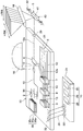
図1に示すように、本実施形態の測距センサは、LD(レーザダイオード)1、変調器2、増幅器3、分波器4、走査部5、受光器6、合波器7、変換器8、TIA(トランスインピーダンスアンプ)9、算出部10を備えている。これらの構成要素は、シリコンフォトニクスによって基板11に形成されており、光集積チップが構成されている。基板11には、さらに、光信号を伝達する光導波路12と、電気信号を伝達する配線13が形成されている。光導波路12は、信号伝達用光導波路に相当する。
図2に示すように、基板11は、Siで構成された支持層11a、SiO2で構成された犠牲層11b、Siで構成された活性層11cが順に積層されたSOI(Silicon on Insulator)基板である。基板11の表面は、例えば一辺が10mmの正方形状とされている。
活性層11cはエッチングにより一部が除去されており、活性層11cと、活性層11cが除去されることによって露出した犠牲層11bは、SiO2で構成された絶縁膜14に覆われている。そして、活性層11cをコア層とし、活性層11cを覆う犠牲層11bおよび絶縁膜14をクラッド層として、光導波路12が構成されている。また、配線13は、絶縁膜14の表面に形成されたAl等の層で構成されている。
本実施形態では、光導波路12のコア層がSiで構成され、クラッド層がSiO2で構成されているが、これらの層を他の材料で構成してもよい。なお、Si、または、不純物がドープされたSiO2、SiN、SiON、LN(LiNbO3)、InPから選択された少なくとも1つの材料で光導波路12のコア層を構成することが好ましい。また、SiO2、SiN、SiON、LN、InGaAsPから選択された少なくとも1つの材料でクラッド層を構成することが好ましい。ただし、コア層とクラッド層は、異なる材料構成とされる。また、コア層の屈折率は、クラッド層よりも高くされている。このような構成では、光導波路12によって光信号が効率よく伝達され、測距センサのSNR(Signal Noise Ratio)が向上する。
また、図3に示すように、測距センサは、ミラー15と、ケース16と、リッド17と、拡散レンズ18と、集光レンズ19とを備えた光学パッケージとされている。ケース16は、一面が開口し、内部に空間が形成された直方体状の枠体であり、セラミック等で構成されている。基板11およびミラー15は、ケース16の内部に配置されている。ケース16の開口部はリッド17によって塞がれており、リッド17の外側には拡散レンズ18および集光レンズ19が配置されている。
測距センサの詳細な構成について説明する。LD1は、外部に照射するための光を発生させるものであり、光源に相当する。本実施形態では、LD1は、DFB(Distributed FeedBack)型のレーザダイオードとされており、基板11上にフリップチップ等で実装されている。具体的には、図1、図4に示すように、LD1は、III-V族半導体で構成された活性層1aと、活性層1aの両側に配置されたp型クラッド層1bおよびn型クラッド層1cとを備えている。また、LD1はn型基板1dを備えており、n型基板1dの一面にn型クラッド層1c、活性層1a、p型クラッド層1bが順に成膜されている。図4に示すように、基板11の一部においては、絶縁膜14と、活性層11cと、犠牲層11bの一部とが除去されており、LD1は、残された犠牲層11bにp型クラッド層1bが積層されるように配置されている。すなわち、犠牲層11bの上に、p型クラッド層1b、活性層1a、n型クラッド層1c、n型基板1dが順に積層されている。LD1は、III-V族半導体で構成されることにより、出力が大きくなる。
本実施形態では、LD1が発生させる光の波長は、0.85μm以上0.95μm以下または1.5μm以上1.6μm以下とされている。図1に示すように、LD1は、光導波路12によって変調器2に接続されており、LD1が発生させた光信号は、変調器2に入力される。なお、図4に示すように、LD1と光導波路12との間には隙間が形成されており、LD1が発生させた光は、この隙間を越えて光導波路12に入る。
変調器2は、LD1が発生させた光の周波数を変調するものである。変調器2として、例えばSSB(Single Side Band)変調器などが用いられる。具体的には、LD1が発生させた光の周波数は、変調器2によって、図5に示すように変化する。すなわち、時間の経過に伴って周波数が増減を繰り返し、時間と周波数との関係を示すグラフが三角波となる。なお、図5のグラフにおいて、実線は変調器2が出力する光信号の周波数を示し、一点鎖線は受光器6から合波器7に入力される光信号の周波数を示す。
図1に示すように、変調器2は、光導波路12によって増幅器3を介して分波器4に接続されており、変調器2によって周波数が変調された光信号は、増幅器3によって増幅された後、分波器4に入力される。
分波器4は、光導波路12が分岐するカプラで構成されており、分波器4に入力された光信号は、一部が走査部5に入力され、他の部分が合波器7に入力される。光導波路12のうち分波器4と走査部5とを接続する部分を光導波路12aとし、分波器4と合波器7とを接続する部分を光導波路12bとする。
前述したように、本実施形態の測距センサは、車外の空間のうち互いに垂直な2方向において所定の範囲に含まれる領域に光を照射し、車外の物体との距離等を検出する。具体的には、測距センサは、車外の空間のうち所定の領域を、水平方向、および、水平面に垂直な方向において複数の領域に分割し、分割された各領域に含まれる物体との距離を算出する。以下、この水平方向および水平面に垂直な方向をそれぞれH方向、V方向とする。
合波器7は、測距センサのV方向の解像度、すなわち、上記所定の領域のV方向の分割数に応じて複数配置されている。そして、分波器4に入力された光信号は、光導波路12bを介して、複数の合波器7に分割されて入力される。
本実施形態では、測距センサの解像度がH方向に1500、V方向に20とされている。そして、これに対応して、合波器7は20個配置され、光導波路12は分波器4において1本の光導波路12aと20本の光導波路12bとに分岐している。
走査部5は、入力された光信号をH方向に走査するものである。本実施形態の走査部5は、OPA(Optical Phased Array)で構成されている。具体的には、図1に示すように、光導波路12aは走査部5において分岐しており、分岐した先の光導波路12を光導波路12cとすると、各光導波路12cに移相器20が配置されている。そして、各光導波路12cは、基板11の側面に至るように形成されており、基板11の側面に露出した光導波路12cから基板11の外部へ光が出射されるようになっている。光導波路12cは、走査用光導波路に相当する。
本実施形態の光導波路12aは、測距センサのH方向の解像度に対応して光導波路12cに分岐しており、移相器20は、光導波路12cと同数配置されている。
移相器20は、図示しない制御回路から入力される電気信号に応じて、分波器4から入力された光信号の位相を変化させるものである。各光導波路12cを通る光信号の位相は各移相器20によって周期的に変化し、これにより、各光導波路12cから出射される光の位相が周期的に変化する。そして、複数の光導波路12cの全体から出射される光の指向性が変化し、光がH方向に走査される。
図3に示すように、基板11およびミラー15は、基板11の側面から出射された光がミラー15に照射されるように、ケース16の内部に配置されている。基板11から出射された光は、ミラー15で反射し、リッド17に照射される。リッド17は、基板11から出射される光を透過させるガラス等で構成されており、リッド17に照射された光はリッド17を透過して拡散レンズ18に照射される。
ミラー15は、拡散レンズ18に照射される光の進行方向が、集光レンズ19から受光器6に照射される光の進行方向と平行となるように、基板11から出射された光の進行方向を調整するものであり、方向調整ミラーに相当する。本実施形態では、ミラー15は、拡散レンズ18に照射される光の進行方向を基板11の表面に垂直な方向に調整するように配置されている。
なお、基板11の表面に垂直な方向には、基板11の表面に完全に垂直な方向のみでなく、略垂直な方向も含まれるものとする。同様に、基板11の表面に平行な方向には、基板11の表面に完全に平行な方向のみでなく、略平行な方向も含まれるものとする。
拡散レンズ18は、照射された光を拡散させてラインビームを形成するものであり、シリンドリカルレンズ等で構成されている。本実施形態の拡散レンズ18は、照射された光をV方向に拡散するように、リッド17の表面に配置されている。拡散レンズ18によって拡散された光は、測距センサの外部に照射される。そして、外部の物体で反射した光は、集光レンズ19に照射される。
集光レンズ19は、リッド17の表面に配置されている。集光レンズ19は、拡散レンズ18から測距センサの外部に照射された光の反射光を集光して受光器6に照射するものであり、リッド17とは反対側に向かって凸形状とされている。受光器6に照射される光の進行方向は、集光レンズ19によって、基板11の表面に垂直とされる。
測距センサの外部から集光レンズ19に照射された光は、リッド17を通って受光器6に照射される。図1に示すように、受光器6は、V方向に並んだ複数の受光アンテナ21を備えており、リッド17を通った光は、各受光アンテナ21に照射される。受光アンテナ21は、測距センサのV方向の解像度に対応して、20個配置されている。
受光アンテナ21は、図6に示すような回折格子で構成されている。なお、図6では、絶縁膜14の図示を省略している。この回折格子は、H方向に平行な軸の両側に広がる扇形状の活性層11cで構成されており、扇形状とされた活性層11cには、扇形状の円周に沿ったスリットが複数形成されている。なお、受光アンテナ21を構成する回折格子を、V方向に平行な軸の両側に広がる扇形状の活性層11cで構成してもよい。
図6に示すように、受光アンテナ21の上には、BPF(バンドパスフィルタ)22と、偏光フィルタ23とが積層されている。BPF22は、所定の周波数帯域の光を通過させ、他の周波数帯域の光を遮断するものである。BPF22は、屈折率の高いTiO2膜24と、屈折率の低いSiO2膜25とが交互に積層されて構成されており、最下層および最上層の両方がTiO2膜24とされている。
偏光フィルタ23は、所定の向きに偏光した光を通過させ、他の向きに偏光した光を遮断するものである。偏光フィルタ23は、BPF22に積層されたSiO2膜26と、SiO2膜26に積層されたAlのワイヤグリッド27とで構成されている。
BPF22、偏光フィルタ23によって、不要なノイズ成分の光が除去され、所定の向きに偏光した所定の周波数帯域の光が受光アンテナ21に照射される。受光アンテナ21は、光導波路12によって合波器7に接続されており、受光アンテナ21が出力した光信号は、合波器7に入力される。
なお、本実施形態の受光アンテナ21は、V方向の幅よりもH方向の幅が大きくされている。これにより、H方向の広い範囲で反射光を受信することができるため、測距センサのSNRが向上する。
合波器7は、分波器4から入力された光信号と受光アンテナ21から入力された光信号との合波により波形を生成するものであり、測距センサのV方向の解像度に対応して複数配置されている。
各合波器7には、分波器4と各受光アンテナ21からの光信号が入力される。そして、各合波器7は、入力された2つの光信号の合波によって形成した光信号を出力する。合波器7は、光導波路12によって変換器8に接続されており、合波器7が形成した光信号は、変換器8に入力される。
変換器8は、入力された光信号を電気信号に変換するものである。本実施形態の変換器8は、PINフォトダイオードで構成されており、入力された光信号に応じて電流信号を出力する。なお、変換器8をアバランシェフォトダイオードで構成してもよい。
なお、本実施形態のようにLD1が発生させる光の波長が0.85μm以上0.95μm以下である場合には、変換器8をSi半導体で構成されたフォトダイオードとすることにより、測距センサのSNRを向上させることができる。また、LD1が発生させる光の波長が1.5μm以上1.6μm以下である場合には、変換器8をGe半導体で構成されたフォトダイオードとすることにより、測距センサのSNRを向上させることができる。
図1に示すように、変換器8は、合波器7と同様に測距センサのV方向の解像度に対応して複数配置されており、各変換器8には、各合波器7から光信号が入力される。変換器8は、配線13によってTIA9に接続されている。TIA9は、変換器8と同様に基板11に複数配置されており、各変換器8が出力する電流信号は、各TIA9に入力される。
TIA9は、変換器8から入力された電流信号を電圧信号に変換して出力する。TIA9は配線13によって算出部10に接続されており、TIA9が出力する電圧信号は、算出部10に入力される。
このような受光アンテナ21、合波器7、変換器8、TIA9は、半導体技術のバッチプロセスを用いて、基板11にそれぞれ複数形成することができる。
算出部10は、入力された電気信号を処理し、ヘテロダイン検波により物体との距離等を算出するものであり、ADC(ADコンバータ)28、FFT(高速フーリエ変換)回路29、画像化処理回路30を備えている。変換器8、TIA9、算出部10は、処理部に相当する。
ADC28は、TIA9が出力した電気信号をデジタル信号に変換して出力するものである。FFT回路29は、ADC28が出力したデジタル信号に含まれる周波数成分を検出するものである。
画像化処理回路30は、FFT回路29によって検出された周波数成分に基づいて物体との距離および物体の速度を算出し、2次元のデータを形成するものである。画像化処理回路30が形成したデータは、車両に搭載された図示しないECU等に送信され、物体との衝突を回避するための自動ブレーキ等に用いられる。
以上が本実施形態の測距センサの構成である。なお、LD1、変調器2、変換器8、TIA9、算出部10、移相器20は、図示しない配線によって外部の制御回路に接続されており、この制御回路から入力される電気信号に応じて動作する。
本実施形態の測距センサの動作について説明する。本実施形態の測距センサは、レーザ光の可干渉性を利用したFMCW方式によって物体との距離および物体の速度を検出する。
まず、LD1が光を発生させると、LD1から変調器2に光信号が入力される。変調器2は、入力された光信号の周波数を周期的に増減させて、図5の実線で示すような三角波を形成する。ここでは、変調器2は、f0を中心としてf0-Δf/2からf0+Δf/2の間で周波数の増減を繰り返す周期Tの三角波を形成する。変調器2が形成した光信号は、増幅器3によって増幅された後、分波器4を介して走査部5および合波器7に入力される。
走査部5は、入力された光信号の位相を移相器20によって周期的に変化させる。これにより、基板11の側面から基板11の外部に出射される光の指向性が周期的に変化し、光がH方向に走査される。基板11の側面から基板11の外部に出射された光は、ミラー15で反射し、進行方向が基板11の表面に垂直な方向とされて、リッド17および拡散レンズ18に照射される。
拡散レンズ18に照射された光は、V方向に拡散されて、車両の外部に照射される。このとき、光がV方向に拡散されているため、図7に示すように、V方向の広い範囲に一度に光を照射することができる。
すなわち、光を照射する領域をH方向にm分割し、V方向にn分割したときの、H方向のi番目、V方向のj番目の領域を領域Ri、jとすると、図7の破線で示すように、領域R1、1~R1、nに一度に光を照射することができる。そして、走査部5が光をH方向に走査することにより、領域Ri、1~Ri、nに一度に光を照射することができる。本実施形態のように測距センサのV方向の解像度が20とされている場合には、領域Ri、1~Ri、20に光を照射することができる。
車両の外部に照射された光は、車両の外部の物体で反射して、集光レンズ19に照射され、集光レンズ19、リッド17、偏光フィルタ23、BPF22を通って受光アンテナ21に照射される。図8に示すように、複数の受光アンテナ21はV方向に並んでいるため、V方向に並んだ複数の領域に含まれる物体で反射された光を一度に受信することができる。例えば、領域R1、1~R1、nに含まれる物体での反射光は図8中の領域R1に照射され、領域Rm、1~Rm、nに含まれる物体での反射光は領域R2に照射される。そして、複数の受光アンテナ21には、領域Ri、1~Ri、nに含まれる物体での反射光がそれぞれ照射される。
受光アンテナ21に照射された光は、合波器7に入力され、分波器4から合波器7に入力された光信号と合成される。合波器7が2つの光信号を合波することで形成された光信号は、変換器8によって電流信号に変換され、さらにTIA9によって電圧信号に変換されて、算出部10に入力される。
なお、各合波器7、各変換器8、各TIA9は、各受光アンテナ21について、光信号の処理等を同時に行う。すなわち、複数の合波器7によって、領域Ri、1~Ri、nからの反射光と分波器4から入力された光信号との合波が、各領域について同時に行われる。そして、複数の変換器8と複数のTIA9によって、合波器7が形成した光信号の電気信号への変換が、各領域について同時に行われる。
算出部10に入力された信号は、ADC28によってデジタル信号に変換され、FFT回路29に入力される。FFT回路29は、入力された信号の周波数成分を検出し、画像化処理回路30は、検出された周波数成分に基づいて、物体との距離および物体の速度を算出する。
合波器7に受光アンテナ21から入力される光と分波器4から入力される光との間には、物体との距離および物体の速度によって、図5に示すように位相および周波数の差が生じる。
そして、合波器7によって形成された光信号には、合成される前の2つの光信号の位相の差と周波数の差によって、2つのビート周波数が現れる。一方のビート周波数fB1は、2つの光の周波数が共に増加しているときの周波数の差であり、他方のビート周波数fB2は、2つの光の周波数が共に減少しているときの周波数の差である。
これら2つのビート周波数は、物体との距離および物体の速度に依存するため、2つのビート周波数から、これらを算出することができる。具体的には、物体との距離をl、物体の測距センサに対する相対速度をv、光速をcとすると、l=cT(fB1+fB2)/8Δf、v=c(fB2-fB1)/4f0となる。
物体との距離および物体の速度の算出は、走査部5が光をH方向に走査する度に行われる。すなわち、領域Ri、1~Ri、nに光が照射され、領域Ri、1~Ri、nに含まれる物体との距離等が算出されると、走査部5は光の進行方向を変化させる。これにより、図7の矢印A1のように、光が照射される領域が変化する。そして、領域Ri+1、1~Ri+1、nに光が照射され、領域Ri+1、1~Ri+1、nに含まれる物体との距離等が算出される。このような動作をi=1~mについて順に行うことにより、領域R1、1~Rm、nに含まれる物体との距離等が算出される。i=mのときに物体との距離等の算出が終了すると、測距センサはi=1として、同様の動作を繰り返す。
画像化処理回路30は、i=mのときの物体との距離等の算出が終了する度に、算出された距離および速度に基づいて2次元のデータを形成し、図示しないECU等に送信する。これにより、車両から近い場所に物体がある場合には、物体との衝突を回避するための自動ブレーキ等が作動する。
本実施形態の効果について説明する。従来の測距センサは、図9に示すように、破線で囲まれる領域、すなわち、領域R1、1~Rm、nのうちの1つに光を照射し、矢印A2、A3のように光をH方向およびV方向の両方に走査し、各領域に含まれる物体との距離等を順に算出していた。
これに対して、本実施形態では、基板11から出射された光が拡散レンズ18によってV方向に拡散されるため、V方向の広い範囲に一度に光を照射することができる。また、複数の受光アンテナ21がV方向に並んでおり、さらに、各受光アンテナ21に対応して合波器7、変換器8、TIA9が配置されている。そのため、V方向の広い範囲からの反射光を一度に受信し、各受光アンテナ21からの信号を並列処理して物体との距離等を算出することができる。
したがって、H方向の走査のみによって、所定の領域に含まれる物体との距離等を算出し、2次元のデータを形成することができる。これにより、高フレームレートで測距の動作をすることが可能となり、測距センサを高速で移動する車両等に搭載して用いることができる。また、基板11から出射された光をH方向のみに走査する本実施形態では、光をH方向およびV方向の両方に走査する場合に比べて、走査の制御が容易である。
また、本実施形態では、光導波路12が基板11の側面に至るように形成されているので、基板11の側面から光を高効率に出射することができる。これにより、測距センサのSNRが向上する。なお、基板11の側面に受光アンテナ21を形成することは困難であり、物体での反射光を基板11の表面に形成された受光アンテナ21に照射するためには、基板11の側面から出射された光と物体での反射光のいずれかをミラーで反射する必要がある。本実施形態では、上記のように、出射光をミラー15で反射することで出射光の進行方向を基板11の表面に垂直にしている。これにより、基板11の表面に形成された受光アンテナ21に物体での反射光が照射されるようになり、測距センサをLIDARとして使用することができる。
また、本実施形態では、受光アンテナ21がH方向に長い形状とされているため、SNRが向上し、例えば車載用途で要求される100m以上の長距離検知を行うことができる。
また、本実施形態では、走査部5が基板11に形成されているため、走査部5を基板11の外部に配置する場合に比べて、測距センサを小型化することができる。
また、本実施形態では、受光アンテナ21の上にBPF22および偏光フィルタ23を積層することにより、これらのフィルタを基板11とは別に配置する場合に比べて、測距センサを小型化することができる。
(第2実施形態)
第2実施形態について説明する。第2実施形態は、第1実施形態に対して算出部10の配置を変更したものであり、その他については第1実施形態と同様であるため、第1実施形態と異なる部分についてのみ説明する。
第2実施形態について説明する。第2実施形態は、第1実施形態に対して算出部10の配置を変更したものであり、その他については第1実施形態と同様であるため、第1実施形態と異なる部分についてのみ説明する。
図10に示すように、本実施形態の測距センサは、基板11とは別の基板31を備えている。そして、算出部10が基板31に形成されている。なお、基板31はケース16の内部に配置されていてもよいし、外部に配置されていてもよい。
基板11および基板31には、それぞれ、導電材料で構成されたパッド32、パッド33が形成されており、パッド32とパッド33はボンディングワイヤ34で接続されている。基板11に形成されたTIA9と、基板31に形成された算出部10は、パッド32、パッド33、ボンディングワイヤ34によって接続されている。
第1実施形態において基板11に形成された構成要素は、光導波路12を介して光信号によって情報が伝達される光回路部と、配線13を介して電気信号によって情報が伝達される電気回路部とに分けられる。そして、光導波路12の最小線幅等で定まる光回路部のプロセスルールが配線13を含む電気回路部のプロセスルールと大きく異なる場合、プロセスルールの差異によって、測距センサの製造コストが増加することがある。
そこで、電気回路部の一部である算出部10を、光回路部が形成された基板11とは別の基板31に形成することにより、プロセスルールの差異による製造コストの増加を抑制することができる。また、光回路部と電気回路部とで歩留まりに差がある場合にも、これらを別々の基板に形成することで、製造コストの増加を抑制することができる。
(第3実施形態)
第3実施形態について説明する。第3実施形態は、第2実施形態に対して光源の構成を変更したものであり、その他については第2実施形態と同様であるため、第2実施形態と異なる部分についてのみ説明する。
第3実施形態について説明する。第3実施形態は、第2実施形態に対して光源の構成を変更したものであり、その他については第2実施形態と同様であるため、第2実施形態と異なる部分についてのみ説明する。
図11に示すように、本実施形態では、外部に照射する光を発生させる光源が、SOA(半導体光増幅器)35と、共振器36で構成されている。
SOA35は、III-V族半導体で構成された活性層35aと、活性層35aの両側に配置されたp型クラッド層35bおよびn型クラッド層35cとを備えている。そして、これらの層は、基板11の上に、p型クラッド層35b、活性層35a、n型クラッド層35cの順にフリップチップ等で積層されている。SOA35は、III-V族半導体で構成されることにより、出力が大きくなる。共振器36としては、例えばダブルリング共振器等が用いられる。
共振器36と変調器2を接続する光導波路12の一部はカプラを構成しており、SOA35と共振器36で構成された光源が発生させた光は、このカプラを介して変調器2へ伝搬する。なお、図11では、カプラとして方向性結合器を用いた例を示しているが、多モード干渉(MMI:Multimode Interference)カプラを用いてもよい。
光源をSOA35と共振器36で構成した本実施形態では、共振器36の共振器長を長くすることで、SOA35が発生させるレーザ光の線幅を、DFBレーザで構成されたLD1が発生させるレーザ光の線幅よりも狭くすることが可能である。したがって、物体との距離の検出精度を向上させることができる。
(第4実施形態)
第4実施形態について説明する。第4実施形態は、第3実施形態に対して走査部5の構成を変更したものであり、その他については第3実施形態と同様であるため、第3実施形態と異なる部分についてのみ説明する。
第4実施形態について説明する。第4実施形態は、第3実施形態に対して走査部5の構成を変更したものであり、その他については第3実施形態と同様であるため、第3実施形態と異なる部分についてのみ説明する。
図12に示すように、本実施形態の走査部5は、複数の光スイッチ37を備えている。光スイッチ37は、各光導波路12cに配置されており、マイクロヒータ38を備えている。マイクロヒータ38は、光導波路12cの温度を変化させ、光導波路12cを通過する光信号の周波数帯域を変化させるものである。マイクロヒータ38は、熱源に相当する。
各光導波路12cは、基板11の側面に対し、互いに異なる角度で傾斜しており、各光導波路12cから互いに異なる角度で光が出射されるようになっている。基板11の側面には、照射された光を平行光とするコリメートレンズ39が複数形成されており、各光導波路12cは、コリメートレンズ39に接続されている。光導波路12cを通過した光は、コリメートレンズ39を介してミラー15に照射される。
光導波路12aは、第1実施形態と同様に、測距センサのH方向の解像度に対応して光導波路12cに分岐しており、光スイッチ37は、光導波路12cと同数配置されている。
このような構成の本実施形態では、複数の光導波路12cの中から、分波器4からの光信号を通過させる光導波路12cを選択することが可能となる。また、各光導波路12cから互いに異なる角度で光が出射されるため、光信号を通過させる光導波路12cを順に切り替えることで、外部に照射する光をH方向に走査することができる。
走査部5としてOPAを用いる場合、光信号が分割されて基板11の側面から出射されるが、走査部5に光スイッチ37を用いる場合、光信号が分割されず、選択された1つの光導波路12から光が出射される。そのため、分波損失が小さく、走査部5としてOPAを用いる場合に比べて、光の利用効率が高い。また、光の出射角度が選択された光導波路12cの角度によって定まるので、光の出射角度の把握が容易である。
(第5実施形態)
第5実施形態について説明する。第5実施形態は、第3実施形態に対して変調器2の位置と走査部5の構成を変更したものであり、その他については第3実施形態と同様であるため、第3実施形態と異なる部分についてのみ説明する。
第5実施形態について説明する。第5実施形態は、第3実施形態に対して変調器2の位置と走査部5の構成を変更したものであり、その他については第3実施形態と同様であるため、第3実施形態と異なる部分についてのみ説明する。
図13に示すように、本実施形態の変調器2は、共振器36の内部に配置されており、共振器36は、光導波路12によって増幅器3に接続されている。共振器36の内部に配置された変調器2は、共振器36内の光導波路の屈折率を変化させることで共振器長を変化させ、周波数変調を行う。変調器2をこのように配置し、共振器長を直接変化させることで、片方の側帯波のみを使用するSSB変調を用いた場合よりも高効率で光を伝搬させることができる。
また、本実施形態の走査部5は、MEMSミラー40で構成されている。また、光導波路12aは、基板11の側面に至っており、分波器4が出力する光信号は、基板11の側面に配置されたコリメートレンズ39を介してMEMSミラー40に照射される。
MEMSミラー40は、Siで構成された支持層、SiO2で構成された犠牲層、Siで構成された活性層が順に積層されたSOI基板を加工することで形成されたものであり、光を反射する反射部41と、反射部41を両持ち支持する梁部42とを備えている。
MEMSミラー40は、例えば圧電素子の変形によって梁部42を振動させる図示しない駆動部を備えており、この駆動部によって梁部42が共振することにより、反射部41が梁部42の軸まわりに揺動する。そして、基板11から出射された光は、揺動する反射部41で反射することにより、進行方向が基板11の表面に略垂直となるとともに、H方向に走査される。MEMSミラー40は、揺動ミラーに相当する。
MEMSミラー40を用いる本実施形態では、分岐損失および導波路損失が生じるOPAや、導波路損失が生じる光スイッチ37を用いる場合に比べて、光の利用効率を向上させることができる。
また、MEMSミラー40では、共振を利用して高速での走査が可能である。また、反射部41を適切な材料で構成することにより、高い反射率が得られる。また、ひずみゲージ等の角度センサを梁部42に設置することで、光が出射される方向を把握することができる。
(第6実施形態)
第6実施形態について説明する。第6実施形態は、第1実施形態に対して基板11から出射される光の進行方向の調整方法を変更したものであり、その他については第1実施形態と同様であるため、第1実施形態と異なる部分についてのみ説明する。
第6実施形態について説明する。第6実施形態は、第1実施形態に対して基板11から出射される光の進行方向の調整方法を変更したものであり、その他については第1実施形態と同様であるため、第1実施形態と異なる部分についてのみ説明する。
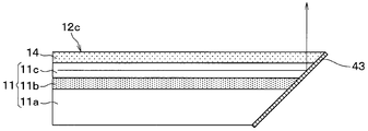
図14に示すように、本実施形態の基板11は、表面に垂直な方向に対して側面が傾斜している。具体的には、側面と表面のなす角が略45度とされている。このような基板11は、エッチングや研磨等により側面と裏面との間の角部を除去することで形成される。
また、基板11の傾斜した側面には、Al等で構成された反射膜43が形成されている。そして、光導波路12cを通った光は、側面に形成された反射膜43で反射して、基板11の表面に垂直な方向に進行方向が変化し、基板11の表面から出射される。
このように傾斜した側面で光の進行方向を調整する本実施形態では、ミラー15が不要となるので、測距センサをさらに小型化することができる。
(第7実施形態)
第7実施形態について説明する。第7実施形態は、第1実施形態に対して基板11から出射される光の進行方向の調整方法を変更したものであり、その他については第1実施形態と同様であるため、第1実施形態と異なる部分についてのみ説明する。
第7実施形態について説明する。第7実施形態は、第1実施形態に対して基板11から出射される光の進行方向の調整方法を変更したものであり、その他については第1実施形態と同様であるため、第1実施形態と異なる部分についてのみ説明する。
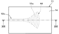
図15、図16に示すように、本実施形態では、光導波路12cの先に回折格子44が形成されている。そして、回折格子44によって、走査部5から送信された光の進行方向が、基板11の表面に平行な方向から基板11の表面に対して傾斜した方向へ変化し、基板11の表面から光が出射される。ミラー15は基板11の表面から出射された送信光を基板11の表面に垂直な方向に反射するように配置されている。
このような構成の本実施形態では、基板11の側面を加工する第6実施形態に比べて、測距センサの製造が容易である。
(第8実施形態)
第8実施形態について説明する。第8実施形態は、第1実施形態に対して受光アンテナ21の構成を変更したものであり、その他については第1実施形態と同様であるため、第1実施形態と異なる部分についてのみ説明する。
第8実施形態について説明する。第8実施形態は、第1実施形態に対して受光アンテナ21の構成を変更したものであり、その他については第1実施形態と同様であるため、第1実施形態と異なる部分についてのみ説明する。
図17に示すように、本実施形態では、受光アンテナ21がH方向とV方向に並ぶ複数の回折格子45で構成されている。そして、回折格子45に対応した数の合波器7および変換器8が配置されており、各回折格子45からの光信号は、各合波器7によって分波器4からの光信号と合成された後、各変換器8に入力される。
回折格子が受信できる光の角度は回折格子の大きさとトレードオフの関係にあるため、回折格子を小さくすることで、広い範囲の角度の光を受信することができる。したがって、基板11において受光器6に用いることができる領域の広さが定まっている場合には、本実施形態のように受光アンテナ21を細分化することで、受光アンテナ21を細分化しない場合に比べて、広い範囲の角度の光を受信することができる。これにより、測距センサのSNRを向上することができる。
(第9実施形態)
第9実施形態について説明する。第9実施形態は、第1実施形態に対して受光アンテナ21の構成を変更したものであり、その他については第1実施形態と同様であるため、第1実施形態と異なる部分についてのみ説明する。
第9実施形態について説明する。第9実施形態は、第1実施形態に対して受光アンテナ21の構成を変更したものであり、その他については第1実施形態と同様であるため、第1実施形態と異なる部分についてのみ説明する。
図18に示すように、本実施形態の受光アンテナ21は、互いに垂直な2方向にスリットが形成された回折格子で構成されており、2方向の偏光に対応している。このような構成では、2方向のうち一方に偏光した光と他方に偏光した光の両方を受信することが可能となり、測距センサのSNRが最大で約2倍に向上する。
(他の実施形態)
なお、本開示は上記した実施形態に限定されるものではなく、適宜変更が可能である。また、上記各実施形態は、互いに無関係なものではなく、組み合わせが明らかに不可な場合を除き、適宜組み合わせが可能である。また、上記各実施形態において、実施形態を構成する要素は、特に必須であると明示した場合および原理的に明らかに必須であると考えられる場合等を除き、必ずしも必須のものではないことは言うまでもない。また、上記各実施形態において、実施形態の構成要素の個数、数値、量、範囲等の数値が言及されている場合、特に必須であると明示した場合および原理的に明らかに特定の数に限定される場合等を除き、その特定の数に限定されるものではない。また、上記各実施形態において、構成要素等の形状、位置関係等に言及するときは、特に明示した場合および原理的に特定の形状、位置関係等に限定される場合等を除き、その形状、位置関係等に限定されるものではない。
なお、本開示は上記した実施形態に限定されるものではなく、適宜変更が可能である。また、上記各実施形態は、互いに無関係なものではなく、組み合わせが明らかに不可な場合を除き、適宜組み合わせが可能である。また、上記各実施形態において、実施形態を構成する要素は、特に必須であると明示した場合および原理的に明らかに必須であると考えられる場合等を除き、必ずしも必須のものではないことは言うまでもない。また、上記各実施形態において、実施形態の構成要素の個数、数値、量、範囲等の数値が言及されている場合、特に必須であると明示した場合および原理的に明らかに特定の数に限定される場合等を除き、その特定の数に限定されるものではない。また、上記各実施形態において、構成要素等の形状、位置関係等に言及するときは、特に明示した場合および原理的に特定の形状、位置関係等に限定される場合等を除き、その形状、位置関係等に限定されるものではない。
例えば、上記第1実施形態では基板11から出射された光をミラー15で反射し、拡散レンズ18に照射される光および受光アンテナ21に照射される光の進行方向を共に基板11の表面に垂直な方向とした。しかしながら、基板11から出射された光をミラー15で反射せず、進行方向を基板11の表面に平行な方向としたまま、拡散レンズ18等を介して外部の空間に照射してもよい。この場合、物体での反射光を図示しないミラーでさらに反射することで、反射光を基板11の表面に形成された受光アンテナ21に照射すればよい。
また、上記第1実施形態では、走査部5は光をH方向に走査し、複数の受光アンテナ21は基板11においてV方向に並んでいる。しかしながら、走査部5が光を走査する方向、および、複数の受光アンテナ21が並ぶ方向は、H方向、V方向に一致していなくてもよく、H方向、V方向に対応した方向とされていればよい。すなわち、走査部5の動作によって測距センサの外部に照射される光がH方向に走査されればよく、拡散レンズ18によって拡散した光の領域Ri、1~Ri、nでの反射光が各受光アンテナ21に照射されるようになっていればよい。また、走査部5が光をV方向に対応する方向に走査し、拡散レンズ18が光をH方向に対応する方向に拡散してもよい。
また、上記第6実施形態において、走査部5をMEMSミラー40で構成してもよい。すなわち、光導波路12aを基板11の側面に至るように形成し、光導波路12aを通って基板11の表面から出射された光をMEMSミラー40で反射して、拡散レンズ18に照射される光をH方向に走査してもよい。
また、上記第7実施形態において、光導波路12aの先に回折格子44を形成し、走査部5および方向調整ミラーをMEMSミラー40で構成してもよい。すなわち、回折格子44を介して基板11の表面から出射された光を、図19に示すようにMEMSミラー40で反射することにより、この光をH方向に走査するとともに、この光の進行方向を基板11の表面に垂直な方向としてもよい。
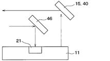
また、図20に示すように、基板11の表面から出射された光をミラー15またはMEMSミラー40で反射することにより、拡散レンズ18に照射される光の進行方向が基板11の表面に平行となるようにしてもよい。この場合、物体での反射光は基板11の表面に平行な方向に進むが、基板11の外側にミラー46を配置し、物体での反射光をミラー46でさらに反射することで、反射光の進行方向を基板11の表面に垂直とし、受光アンテナ21に光を照射することができる。2つの光の進行方向を基板11の表面に平行とする構成では、測距センサの光学設計が容易になる。ミラー46は、受光ミラーに相当する。
また、測距センサが増幅器3を備えていなくてもよい。また、DFB型のレーザダイオードは、発生させた光の周波数を変調する機能を有するため、光源がDFB型のレーザダイオードであるLD1で構成されている場合には、測距センサが変調器2を備えていなくてもよい。変調器2を配置せず、LD1からの光信号が増幅器3、分波器4等に直接入力される構成とすることにより、測距センサを小型化することができる。
また、上記第6実施形態において、基板11の側面に反射膜43が形成されていなくてもよい。また、上記第8実施形態において、受光アンテナ21がH方向またはV方向のいずれか一方に並ぶ複数の回折格子45で構成されていてもよい。
また、上記第4、第5実施形態において、光源がLD1で構成されていてもよい。また、上記第6~第9実施形態において、光源がSOA35および共振器36で構成されていてもよい。また、上記第6~第9実施形態において、算出部10が基板31に形成されていてもよい。
Claims (27)
- 光を発生させる光源(1、35、36)と、前記光源が発生させた光の反射光が照射される受光器(6)とが同一の基板(11)に形成されており、前記光源が発生させた光と前記受光器に照射された光とを用いたヘテロダイン検波により、外部の空間のうち互いに垂直な一方向および他方向における所定の領域に含まれる物体との距離を検出する測距センサであって、
前記光源が発生させた光を前記一方向に対応する方向に走査する走査部(5)と、
前記光源が発生させた光を前記他方向に対応する方向に拡散させる拡散レンズ(18)と、
前記光源が発生させた光と前記受光器に照射された光とを合波して光信号を形成する複数の合波器(7)と、
前記合波器が形成した光信号に基づいて物体との距離を算出する処理部(8、9、10)と、を備え、
前記受光器は、前記他方向に対応する方向に並ぶ複数の受光アンテナ(21)を有し、
複数の前記受光アンテナそれぞれに前記合波器が接続されており、
前記処理部は、前記合波器が形成した光信号に基づく物体との距離の算出を、複数の前記受光アンテナそれぞれについて並列に処理する測距センサ。 - 前記光源が発生させた光の反射光を集光して前記受光アンテナに照射する集光レンズ(19)を備え、
前記光源から前記拡散レンズに照射される光の進行方向は、前記集光レンズから前記受光アンテナに照射される光の進行方向と平行とされている請求項1に記載の測距センサ。 - 前記光源から前記拡散レンズに照射される光の進行方向が、前記集光レンズから前記受光アンテナに照射される光の進行方向と平行となるように、前記光源が発生させた光の進行方向を調整する方向調整ミラー(15)を備える請求項2に記載の測距センサ。
- 前記方向調整ミラーは、前記光源から前記拡散レンズに照射される光の進行方向が、前記基板の表面に垂直となるように、前記光源が発生させた光の進行方向を調整する請求項3に記載の測距センサ。
- 前記方向調整ミラーは、前記光源から前記拡散レンズに照射される光の進行方向が、前記基板の表面に平行となるように、前記光源が発生させた光の進行方向を調整する請求項3に記載の測距センサ。
- 前記走査部は、複数の走査用光導波路(12c)と、複数の前記走査用光導波路それぞれに配置された移相器(20)と、を備え、前記走査用光導波路それぞれから出射される光の位相を変化させることにより、複数の前記走査用光導波路の全体から出射される光の指向性を変化させ、前記光源が発生させた光を前記一方向に対応する方向に走査する請求項1ないし5のいずれか1つに記載の測距センサ。
- 前記走査部は、複数の走査用光導波路(12c)と、複数の前記走査用光導波路それぞれに配置された熱源(38)と、を備え、前記熱源によって前記走査用光導波路の温度を変化させることにより、複数の前記走査用光導波路の中から前記光源が発生させた光を通過させる走査用光導波路を選択し、前記光源が発生させた光を前記一方向に対応する方向に走査する請求項1ないし5のいずれか1つに記載の測距センサ。
- 光を反射する反射部(41)と、前記反射部を両持ち支持する梁部(42)と、を有し、前記梁部の振動により前記反射部が揺動する揺動ミラー(40)を備え、
前記走査部は、前記揺動ミラーで構成されている請求項1ないし5のいずれか1つに記載の測距センサ。 - 前記揺動ミラーは、前記光源が発生させた光の進行方向を前記基板の表面に垂直な方向に調整する請求項8に記載の測距センサ。
- 前記揺動ミラーは、前記光源が発生させた光の進行方向を前記基板の表面に平行な方向に調整する請求項8に記載の測距センサ。
- 前記光源が発生させた光の反射光は、前記基板の外側に配置された受光ミラー(46)によって進行方向が前記基板の表面に垂直な方向に調整された後、前記受光アンテナに照射される請求項5または10に記載の測距センサ。
- 前記光源が発生させた光は、前記基板の側面から出射される請求項1ないし11のいずれか1つに記載の測距センサ。
- 前記光源が発生させた光は、前記基板の表面から出射される請求項1ないし11のいずれか1つに記載の測距センサ。
- 前記光源が発生させた光は、前記基板に形成された回折格子(44)によって進行方向が調整され、前記基板の表面から出射される請求項13に記載の測距センサ。
- 前記基板の側面は、前記基板の表面に垂直な方向に対して傾斜しており、
前記光源が発生させた光は、前記基板の表面に垂直な方向に対して傾斜した側面で反射して、前記基板の表面から出射される請求項13に記載の測距センサ。 - 前記基板の表面に垂直な方向に対して傾斜した側面には、前記光源が発生させた光を反射する反射膜(43)が形成されている請求項15に記載の測距センサ。
- 前記基板に形成され、前記光源が発生させた光の周波数を変調する変調器(2)を備え、
前記光源は、III-V族半導体で構成された活性層(1a)と、前記活性層の両側に配置されたp型クラッド層(1b)およびn型クラッド層(1c)と、を備えるレーザダイオード(1)で構成されている請求項1ないし16のいずれか1つに記載の測距センサ。 - 前記光源は、発生させた光の周波数を変調する機能を有するレーザダイオード(1)で構成されている請求項1ないし16のいずれか1つに記載の測距センサ。
- III-V族半導体で構成された活性層(35a)と、前記活性層の両側に配置されたp型クラッド層(35b)およびn型クラッド層(35c)と、を有する半導体光増幅器(35)と、
前記基板に形成された共振器(36)と、を備え、
前記光源は、前記半導体光増幅器および前記共振器で構成されている請求項1ないし16のいずれか1つに記載の測距センサ。 - 前記受光アンテナは、回折格子で構成されている請求項1ないし19のいずれか1つに記載の測距センサ。
- 複数の前記受光アンテナは、それぞれ、前記一方向に対応する方向、前記他方向に対応する方向のいずれか一方または両方に並ぶ複数の回折格子(45)で構成されている請求項20に記載の測距センサ。
- 前記受光アンテナは、2方向にスリットが形成された回折格子で構成されている請求項20または21に記載の測距センサ。
- 前記受光アンテナに積層されたバンドパスフィルタ(22)および偏光フィルタ(23)を備える請求項1ないし22のいずれか1つに記載の測距センサ。
- 前記基板には、光信号を伝達するための信号伝達用光導波路(12)が形成されており、
前記信号伝達用光導波路のコア層は、Si、または、不純物がドープされたSiO2、SiN、SiON、LN、InPから選択された少なくとも1つの材料で構成されており、前記コア層を覆うクラッド層は、SiO2、SiN、SiON、LN、InGaAsPから選択された少なくとも1つの材料で構成されている請求項1ないし23のいずれか1つに記載の測距センサ。 - 前記合波器が形成した光信号を電気信号に変換する変換器(8)を備え、
前記光源が発生させる光の波長は、0.85μm以上0.95μm以下であり、
前記変換器は、Si半導体で構成されたフォトダイオードである請求項1ないし24のいずれか1つに記載の測距センサ。 - 前記合波器が形成した光信号を電気信号に変換する変換器(8)を備え、
前記光源が発生させる光の波長は、1.5μm以上1.6μm以下であり、
前記変換器は、Ge半導体で構成されたフォトダイオードである請求項1ないし24のいずれか1つに記載の測距センサ。 - 前記処理部の一部は、前記基板とは別の基板(31)に形成されている請求項1ないし26のいずれか1つに記載の測距センサ。
Priority Applications (2)
| Application Number | Priority Date | Filing Date | Title |
|---|---|---|---|
| CN201880034992.6A CN110678774B (zh) | 2017-05-29 | 2018-04-19 | 测距传感器 |
| US16/690,370 US11480679B2 (en) | 2017-05-29 | 2019-11-21 | Distance measurement sensor |
Applications Claiming Priority (2)
| Application Number | Priority Date | Filing Date | Title |
|---|---|---|---|
| JP2017-105871 | 2017-05-29 | ||
| JP2017105871A JP6743761B2 (ja) | 2017-05-29 | 2017-05-29 | 測距センサ |
Related Child Applications (1)
| Application Number | Title | Priority Date | Filing Date |
|---|---|---|---|
| US16/690,370 Continuation US11480679B2 (en) | 2017-05-29 | 2019-11-21 | Distance measurement sensor |
Publications (1)
| Publication Number | Publication Date |
|---|---|
| WO2018221060A1 true WO2018221060A1 (ja) | 2018-12-06 |
Family
ID=64455917
Family Applications (1)
| Application Number | Title | Priority Date | Filing Date |
|---|---|---|---|
| PCT/JP2018/016178 Ceased WO2018221060A1 (ja) | 2017-05-29 | 2018-04-19 | 測距センサ |
Country Status (4)
| Country | Link |
|---|---|
| US (1) | US11480679B2 (ja) |
| JP (1) | JP6743761B2 (ja) |
| CN (1) | CN110678774B (ja) |
| WO (1) | WO2018221060A1 (ja) |
Cited By (6)
| Publication number | Priority date | Publication date | Assignee | Title |
|---|---|---|---|---|
| CN111355535A (zh) * | 2018-12-20 | 2020-06-30 | 罗伯特·博世有限公司 | 用于光电传感器的多通道模/数转换器设备、信号调制方法和距离和/或速度传感器 |
| DE102019124266A1 (de) * | 2019-09-10 | 2021-03-11 | Sick Ag | Optoelektronischer Sensor und Verfahren zum Erfassen von Objekten in einem Überwachungsbereich |
| US20230146113A1 (en) * | 2020-04-21 | 2023-05-11 | Mouro Labs S.L. | Lidar system with suppressed doppler frequency shift |
| JP2025527493A (ja) * | 2022-08-15 | 2025-08-22 | オーロラ・オペレイションズ・インコーポレイティッド | トランシーバデバイスを含むlidarセンサーシステム |
| JP2026500233A (ja) * | 2022-12-30 | 2026-01-06 | オーロラ・オペレイションズ・インコーポレイティッド | モジュール式アセンブリを含む光検出および距離測定システム |
| JP2026501137A (ja) * | 2022-12-30 | 2026-01-14 | オーロラ・オペレイションズ・インコーポレイティッド | 高出力増幅器を含む光検出および距離測定システム |
Families Citing this family (47)
| Publication number | Priority date | Publication date | Assignee | Title |
|---|---|---|---|---|
| US11536805B2 (en) | 2018-06-25 | 2022-12-27 | Silc Technologies, Inc. | Optical switching for tuning direction of LIDAR output signals |
| US10545289B1 (en) * | 2018-08-08 | 2020-01-28 | Lockheed Martin Corporation | Planar optical head for free space optical communications, coherent LIDAR, and other applications |
| US12535586B2 (en) | 2018-08-31 | 2026-01-27 | SiLC Technology, Inc. | Reduction of ADC sampling rates in LIDAR systems |
| EP3914928B1 (en) * | 2019-01-25 | 2024-09-25 | SiLC Technologies, Inc. | Steering of output signals in lidar systems |
| US11635491B2 (en) * | 2019-03-06 | 2023-04-25 | Silc Technologies, Inc. | Amplification of LIDAR output signals |
| JPWO2020189174A1 (ja) * | 2019-03-18 | 2020-09-24 | ||
| JP7211212B2 (ja) | 2019-03-29 | 2023-01-24 | 株式会社デンソー | 測距モジュール |
| US11016195B2 (en) * | 2019-04-26 | 2021-05-25 | Mouro Labs, S.L. | Apparatus and method for managing coherent detection from multiple apertures in a LiDAR system |
| US12429569B2 (en) | 2019-05-17 | 2025-09-30 | Silc Technologies, Inc. | Identification of materials illuminated by LIDAR systems |
| JP2020187079A (ja) * | 2019-05-17 | 2020-11-19 | 三菱重工業株式会社 | レーザレーダ装置及び走行体 |
| JP7209294B2 (ja) * | 2019-05-24 | 2023-01-20 | 株式会社デンソー | グレーティングカプラ、グレーティングカプラアレイ、受光アンテナおよび測距センサ |
| US11650317B2 (en) | 2019-06-28 | 2023-05-16 | Silc Technologies, Inc. | Use of frequency offsets in generation of LIDAR data |
| AU2020320867B2 (en) * | 2019-07-26 | 2024-11-21 | Aurora Operations, Inc. | Focal plane array system for FMCW LiDAR |
| KR102845980B1 (ko) | 2019-08-20 | 2025-08-12 | 삼성전자주식회사 | 라이다 장치 및 그 동작 방법 |
| US11714167B2 (en) * | 2019-08-21 | 2023-08-01 | Silc Technologies, Inc. | LIDAR adapter for use with LIDAR chip |
| US10788340B1 (en) * | 2019-09-12 | 2020-09-29 | Honeywell International Inc. | High resolution and high efficiency photonic air data detection |
| CA3163567A1 (en) * | 2020-01-03 | 2021-07-08 | Sen Lin | High resolution frequency modulated continuous wave lidar with solid-state beam steering |
| KR102778198B1 (ko) * | 2020-01-07 | 2025-03-10 | 삼성전자주식회사 | 광 검출 소자 및 이를 포함하는 광 시스템 |
| WO2021146116A1 (en) | 2020-01-13 | 2021-07-22 | Ours Technology Inc. | Silicon-assisted packaging of high power integrated soa array |
| US11209529B2 (en) | 2020-03-05 | 2021-12-28 | Aurora Operations, Inc. | Coherent signal combining with multiple-outputs for quasi-CW LIDAR operation |
| JP2023099238A (ja) * | 2020-05-27 | 2023-07-12 | パナソニックIpマネジメント株式会社 | 計測装置 |
| US11280909B2 (en) | 2020-06-29 | 2022-03-22 | Aurora Operations, Inc. | Lidar transmit/receive system |
| US10948600B1 (en) | 2020-06-29 | 2021-03-16 | Aurora Innovation, Inc. | Systems and methods for IQ detection |
| CN112639514B (zh) * | 2020-07-07 | 2024-02-23 | 深圳市速腾聚创科技有限公司 | 激光接收装置、激光雷达及智能感应设备 |
| CN111880188B (zh) * | 2020-08-07 | 2023-07-07 | 国科光芯(海宁)科技股份有限公司 | 一种光学相干测距装置及方法 |
| US12306344B1 (en) * | 2020-08-25 | 2025-05-20 | Silc Technologies, Inc. | Reduction of components in LIDAR systems |
| CN112051582A (zh) * | 2020-09-28 | 2020-12-08 | 国科光芯(海宁)科技股份有限公司 | 一种阵列式相干测距芯片及其系统 |
| US11789149B2 (en) * | 2020-10-04 | 2023-10-17 | Silc Technologies, Inc. | Polarization separation in remote imaging systems |
| JP7452374B2 (ja) * | 2020-10-20 | 2024-03-19 | 株式会社Soken | 物体検知装置および物体検知プログラム |
| US11988774B2 (en) * | 2020-10-26 | 2024-05-21 | Honeywell International Inc. | Integrated photonics air data system |
| KR102556165B1 (ko) * | 2020-11-04 | 2023-07-14 | 성균관대학교산학협력단 | 일체형 opa 소자 및 이를 포함하는 광센싱 시스템 |
| US11454709B2 (en) * | 2020-11-23 | 2022-09-27 | Ours Technology, Llc | Optical coupler for LIDAR sensor |
| WO2022118647A1 (ja) * | 2020-12-04 | 2022-06-09 | パナソニックホールディングス株式会社 | 光周波数コム装置および計測装置 |
| KR102614185B1 (ko) * | 2020-12-15 | 2023-12-15 | 부산대학교 산학협력단 | 폴리머 광ic 기반 레이저 집적형 이차원 빔스캐너 및 그의 제조 방법 |
| US12078754B1 (en) * | 2020-12-30 | 2024-09-03 | Waymo Llc | Lidar transmitter assembly |
| JP7405118B2 (ja) * | 2021-05-28 | 2023-12-26 | 株式会社デンソー | レーザレーダ装置 |
| US12541009B2 (en) * | 2021-06-17 | 2026-02-03 | Silc Technologies, Inc. | Scanning multiple LIDAR system output signals |
| EP4379415A4 (en) * | 2021-07-28 | 2025-02-12 | Sony Semiconductor Solutions Corporation | SENSOR DEVICE AND ELECTRONIC EQUIPMENT |
| US12411213B2 (en) | 2021-10-11 | 2025-09-09 | Silc Technologies, Inc. | Separation of light signals in a LIDAR system |
| US12553995B2 (en) | 2022-02-14 | 2026-02-17 | Silc Technologies, Inc. | Data refinement in optical systems |
| US12578443B2 (en) | 2022-04-23 | 2026-03-17 | Silc Technologies, Inc. | Data refinement in optical imaging systems |
| US20230375713A1 (en) * | 2022-05-20 | 2023-11-23 | Ours Technology, Llc | Lidar with switchable local oscillator signals |
| JP7718325B2 (ja) * | 2022-05-25 | 2025-08-05 | 株式会社デンソー | 光送受信装置 |
| US11619739B1 (en) * | 2022-06-09 | 2023-04-04 | Ours Technology, Llc | LIDAR pixel with dual polarization receive optical antenna |
| US12422618B2 (en) | 2022-10-13 | 2025-09-23 | Silc Technologies, Inc. | Buried taper with reflecting surface |
| EP4628926A4 (en) * | 2022-11-29 | 2026-04-01 | Sony Semiconductor Solutions Corp | LIGHT DETECTION DEVICE AND LIGHT DETECTION SYSTEM |
| US12578439B2 (en) | 2023-04-11 | 2026-03-17 | Silc Technologies, Inc. | Increasing resolution in imaging systems |
Citations (3)
| Publication number | Priority date | Publication date | Assignee | Title |
|---|---|---|---|---|
| US20150293224A1 (en) * | 2013-05-09 | 2015-10-15 | Quanergy Systems, Inc. | Solid state optical phased array lidar and method of using same |
| JP2016014665A (ja) * | 2014-07-03 | 2016-01-28 | アドヴァンスド サイエンティフィック コンセプツ,イン | 密集環境のladarセンサ |
| JP2016180624A (ja) * | 2015-03-23 | 2016-10-13 | 三菱重工業株式会社 | レーザレーダ装置及び走行体 |
Family Cites Families (14)
| Publication number | Priority date | Publication date | Assignee | Title |
|---|---|---|---|---|
| GB2367199B (en) * | 2000-09-20 | 2005-01-26 | Parthus | Apparatus for receiving ranging signals |
| TWI294262B (en) * | 2002-06-28 | 2008-03-01 | Matsushita Electric Industrial Co Ltd | A light reception/emission device built-in module with optical and electrical wiring combined therein and method of making the same |
| TWI250301B (en) * | 2004-03-17 | 2006-03-01 | Asia Optical Co Inc | The optical system of laser meter |
| JP2006023626A (ja) * | 2004-07-09 | 2006-01-26 | Olympus Corp | コリメーション調整機構、それを用いた光アンテナ装置およびコリメーション調整方法 |
| JP4696319B2 (ja) * | 2007-02-05 | 2011-06-08 | 日本電信電話株式会社 | フィルタ方式高速波長掃引光源 |
| JP5758851B2 (ja) | 2012-06-15 | 2015-08-05 | 日立オートモティブシステムズ株式会社 | 熱式流量計 |
| JP6045963B2 (ja) * | 2013-04-05 | 2016-12-14 | 日立マクセル株式会社 | 光測距装置 |
| WO2015087380A1 (ja) | 2013-12-09 | 2015-06-18 | 三菱電機株式会社 | レーザレーダ装置 |
| JP6146295B2 (ja) | 2013-12-26 | 2017-06-14 | 株式会社豊田中央研究所 | レーダ装置および速度の方向測定方法 |
| JP6241283B2 (ja) | 2014-01-06 | 2017-12-06 | 株式会社豊田中央研究所 | レーダ装置および距離速度測定方法 |
| JP6204272B2 (ja) * | 2014-06-05 | 2017-09-27 | 日本電信電話株式会社 | 距離計測装置 |
| US9916713B1 (en) * | 2014-07-09 | 2018-03-13 | Cummins-Allison Corp. | Systems, methods and devices for processing coins utilizing normal or near-normal and/or high-angle of incidence lighting |
| JP6424801B2 (ja) | 2014-11-19 | 2018-11-21 | 株式会社豊田中央研究所 | レーザレーダ装置およびレーザレーダ装置の光受信方法 |
| GB2563546B (en) * | 2016-03-29 | 2021-12-22 | Nec Corp | Communication apparatus and communication method |
-
2017
- 2017-05-29 JP JP2017105871A patent/JP6743761B2/ja active Active
-
2018
- 2018-04-19 CN CN201880034992.6A patent/CN110678774B/zh active Active
- 2018-04-19 WO PCT/JP2018/016178 patent/WO2018221060A1/ja not_active Ceased
-
2019
- 2019-11-21 US US16/690,370 patent/US11480679B2/en active Active
Patent Citations (3)
| Publication number | Priority date | Publication date | Assignee | Title |
|---|---|---|---|---|
| US20150293224A1 (en) * | 2013-05-09 | 2015-10-15 | Quanergy Systems, Inc. | Solid state optical phased array lidar and method of using same |
| JP2016014665A (ja) * | 2014-07-03 | 2016-01-28 | アドヴァンスド サイエンティフィック コンセプツ,イン | 密集環境のladarセンサ |
| JP2016180624A (ja) * | 2015-03-23 | 2016-10-13 | 三菱重工業株式会社 | レーザレーダ装置及び走行体 |
Non-Patent Citations (1)
| Title |
|---|
| SUNI, PAUL ET AL.: "Photonic Integrated Circuits for Coherent Lidar", 18TH COHERENT LASER RADAR CONFERENCE (CLRC 2016), June 2016 (2016-06-01), XP055561803, ISBN: 978-1-510828544 * |
Cited By (9)
| Publication number | Priority date | Publication date | Assignee | Title |
|---|---|---|---|---|
| CN111355535A (zh) * | 2018-12-20 | 2020-06-30 | 罗伯特·博世有限公司 | 用于光电传感器的多通道模/数转换器设备、信号调制方法和距离和/或速度传感器 |
| CN111355535B (zh) * | 2018-12-20 | 2024-09-20 | 罗伯特·博世有限公司 | 用于光电传感器的多通道模/数转换器设备、信号调制方法和距离和/或速度传感器 |
| DE102019124266A1 (de) * | 2019-09-10 | 2021-03-11 | Sick Ag | Optoelektronischer Sensor und Verfahren zum Erfassen von Objekten in einem Überwachungsbereich |
| EP3792668A1 (de) * | 2019-09-10 | 2021-03-17 | Sick Ag | Optoelektronischer sensor und verfahren zum erfassen von objekten in einem überwachungsbereich |
| US20230146113A1 (en) * | 2020-04-21 | 2023-05-11 | Mouro Labs S.L. | Lidar system with suppressed doppler frequency shift |
| US11815599B2 (en) * | 2020-04-21 | 2023-11-14 | Mouro Labs, S.L. | Lidar system with suppressed doppler frequency shift |
| JP2025527493A (ja) * | 2022-08-15 | 2025-08-22 | オーロラ・オペレイションズ・インコーポレイティッド | トランシーバデバイスを含むlidarセンサーシステム |
| JP2026500233A (ja) * | 2022-12-30 | 2026-01-06 | オーロラ・オペレイションズ・インコーポレイティッド | モジュール式アセンブリを含む光検出および距離測定システム |
| JP2026501137A (ja) * | 2022-12-30 | 2026-01-14 | オーロラ・オペレイションズ・インコーポレイティッド | 高出力増幅器を含む光検出および距離測定システム |
Also Published As
| Publication number | Publication date |
|---|---|
| US20200088876A1 (en) | 2020-03-19 |
| US11480679B2 (en) | 2022-10-25 |
| CN110678774B (zh) | 2023-05-05 |
| CN110678774A (zh) | 2020-01-10 |
| JP2018200273A (ja) | 2018-12-20 |
| JP6743761B2 (ja) | 2020-08-19 |
Similar Documents
| Publication | Publication Date | Title |
|---|---|---|
| JP6743761B2 (ja) | 測距センサ | |
| JP7039948B2 (ja) | 測距センサ | |
| US20260036677A1 (en) | Modular three-dimensional optical sensing system | |
| US12429746B2 (en) | Optical beam scanning based on waveguide switching and position-to-angle conversion of a lens and applications | |
| CN113678020B (zh) | 用于成像的光学部件 | |
| US11002832B2 (en) | Chip-scale LIDAR with a single 2D MEMS scanner | |
| CN107765363B (zh) | 光学相控阵列(OPA)及包括其的光集成电路和LiDAR系统 | |
| US9735885B1 (en) | Chip-scale mid-IR scanning frequency modulated coherent ladar receiver | |
| US10605901B2 (en) | Beam steering device and optical apparatus including the same | |
| JP2022521459A (ja) | スペックル感度が低減されたlidarシステム | |
| JP2020517912A (ja) | 波長分割多重通信lidar | |
| WO2018003852A1 (ja) | 光偏向デバイスおよびライダー装置 | |
| JP7209294B2 (ja) | グレーティングカプラ、グレーティングカプラアレイ、受光アンテナおよび測距センサ | |
| CN116908815B (zh) | 激光雷达及可移动设备 | |
| CN118355294A (zh) | 光电子器件和激光雷达系统 | |
| CN113661408B (zh) | 用于扫描lidar的光学部件 |
Legal Events
| Date | Code | Title | Description |
|---|---|---|---|
| 121 | Ep: the epo has been informed by wipo that ep was designated in this application |
Ref document number: 18809075 Country of ref document: EP Kind code of ref document: A1 |
|
| NENP | Non-entry into the national phase |
Ref country code: DE |
|
| 122 | Ep: pct application non-entry in european phase |
Ref document number: 18809075 Country of ref document: EP Kind code of ref document: A1 |