WO2018235137A1 - 半導体装置 - Google Patents
半導体装置 Download PDFInfo
- Publication number
- WO2018235137A1 WO2018235137A1 PCT/JP2017/022567 JP2017022567W WO2018235137A1 WO 2018235137 A1 WO2018235137 A1 WO 2018235137A1 JP 2017022567 W JP2017022567 W JP 2017022567W WO 2018235137 A1 WO2018235137 A1 WO 2018235137A1
- Authority
- WO
- WIPO (PCT)
- Prior art keywords
- gan
- conductive pattern
- mos
- hemt
- pattern portion
- Prior art date
- Legal status (The legal status is an assumption and is not a legal conclusion. Google has not performed a legal analysis and makes no representation as to the accuracy of the status listed.)
- Ceased
Links
Images


Classifications
-
- H—ELECTRICITY
- H10—SEMICONDUCTOR DEVICES; ELECTRIC SOLID-STATE DEVICES NOT OTHERWISE PROVIDED FOR
- H10W—GENERIC PACKAGES, INTERCONNECTIONS, CONNECTORS OR OTHER CONSTRUCTIONAL DETAILS OF DEVICES COVERED BY CLASS H10
- H10W42/00—Arrangements for protection of devices
-
- H—ELECTRICITY
- H02—GENERATION; CONVERSION OR DISTRIBUTION OF ELECTRIC POWER
- H02M—APPARATUS FOR CONVERSION BETWEEN AC AND AC, BETWEEN AC AND DC, OR BETWEEN DC AND DC, AND FOR USE WITH MAINS OR SIMILAR POWER SUPPLY SYSTEMS; CONVERSION OF DC OR AC INPUT POWER INTO SURGE OUTPUT POWER; CONTROL OR REGULATION THEREOF
- H02M3/00—Conversion of DC power input into DC power output
- H02M3/22—Conversion of DC power input into DC power output with intermediate conversion into AC
- H02M3/24—Conversion of DC power input into DC power output with intermediate conversion into AC by static converters
- H02M3/28—Conversion of DC power input into DC power output with intermediate conversion into AC by static converters using discharge tubes with control electrode or semiconductor devices with control electrode to produce the intermediate AC
- H02M3/325—Conversion of DC power input into DC power output with intermediate conversion into AC by static converters using discharge tubes with control electrode or semiconductor devices with control electrode to produce the intermediate AC using devices of a triode or a transistor type requiring continuous application of a control signal
- H02M3/335—Conversion of DC power input into DC power output with intermediate conversion into AC by static converters using discharge tubes with control electrode or semiconductor devices with control electrode to produce the intermediate AC using devices of a triode or a transistor type requiring continuous application of a control signal using semiconductor devices only
-
- H—ELECTRICITY
- H10—SEMICONDUCTOR DEVICES; ELECTRIC SOLID-STATE DEVICES NOT OTHERWISE PROVIDED FOR
- H10D—INORGANIC ELECTRIC SEMICONDUCTOR DEVICES
- H10D30/00—Field-effect transistors [FET]
- H10D30/01—Manufacture or treatment
- H10D30/015—Manufacture or treatment of FETs having heterojunction interface channels or heterojunction gate electrodes, e.g. HEMT
-
- H—ELECTRICITY
- H10—SEMICONDUCTOR DEVICES; ELECTRIC SOLID-STATE DEVICES NOT OTHERWISE PROVIDED FOR
- H10D—INORGANIC ELECTRIC SEMICONDUCTOR DEVICES
- H10D30/00—Field-effect transistors [FET]
- H10D30/40—FETs having zero-dimensional [0D], one-dimensional [1D] or two-dimensional [2D] charge carrier gas channels
- H10D30/47—FETs having zero-dimensional [0D], one-dimensional [1D] or two-dimensional [2D] charge carrier gas channels having two-dimensional [2D] charge carrier gas channels, e.g. nanoribbon FETs or high electron mobility transistors [HEMT]
-
- H—ELECTRICITY
- H10—SEMICONDUCTOR DEVICES; ELECTRIC SOLID-STATE DEVICES NOT OTHERWISE PROVIDED FOR
- H10D—INORGANIC ELECTRIC SEMICONDUCTOR DEVICES
- H10D62/00—Semiconductor bodies, or regions thereof, of devices having potential barriers
- H10D62/80—Semiconductor bodies, or regions thereof, of devices having potential barriers characterised by the materials
- H10D62/85—Semiconductor bodies, or regions thereof, of devices having potential barriers characterised by the materials being Group III-V materials, e.g. GaAs
- H10D62/8503—Nitride Group III-V materials, e.g. AlN or GaN
-
- H—ELECTRICITY
- H10—SEMICONDUCTOR DEVICES; ELECTRIC SOLID-STATE DEVICES NOT OTHERWISE PROVIDED FOR
- H10W—GENERIC PACKAGES, INTERCONNECTIONS, CONNECTORS OR OTHER CONSTRUCTIONAL DETAILS OF DEVICES COVERED BY CLASS H10
- H10W20/00—Interconnections in chips, wafers or substrates
- H10W20/40—Interconnections external to wafers or substrates, e.g. back-end-of-line [BEOL] metallisations or vias connecting to gate electrodes
- H10W20/41—Interconnections external to wafers or substrates, e.g. back-end-of-line [BEOL] metallisations or vias connecting to gate electrodes characterised by their conductive parts
- H10W20/43—Layouts of interconnections
-
- H—ELECTRICITY
- H10—SEMICONDUCTOR DEVICES; ELECTRIC SOLID-STATE DEVICES NOT OTHERWISE PROVIDED FOR
- H10W—GENERIC PACKAGES, INTERCONNECTIONS, CONNECTORS OR OTHER CONSTRUCTIONAL DETAILS OF DEVICES COVERED BY CLASS H10
- H10W40/00—Arrangements for thermal protection or thermal control
- H10W40/20—Arrangements for cooling
- H10W40/25—Arrangements for cooling characterised by their materials
- H10W40/255—Arrangements for cooling characterised by their materials having a laminate or multilayered structure, e.g. direct bond copper [DBC] ceramic substrates
-
- H—ELECTRICITY
- H10—SEMICONDUCTOR DEVICES; ELECTRIC SOLID-STATE DEVICES NOT OTHERWISE PROVIDED FOR
- H10W—GENERIC PACKAGES, INTERCONNECTIONS, CONNECTORS OR OTHER CONSTRUCTIONAL DETAILS OF DEVICES COVERED BY CLASS H10
- H10W44/00—Electrical arrangements for controlling or matching impedance
- H10W44/501—Inductive arrangements
-
- H—ELECTRICITY
- H10—SEMICONDUCTOR DEVICES; ELECTRIC SOLID-STATE DEVICES NOT OTHERWISE PROVIDED FOR
- H10W—GENERIC PACKAGES, INTERCONNECTIONS, CONNECTORS OR OTHER CONSTRUCTIONAL DETAILS OF DEVICES COVERED BY CLASS H10
- H10W90/00—Package configurations
-
- H—ELECTRICITY
- H10—SEMICONDUCTOR DEVICES; ELECTRIC SOLID-STATE DEVICES NOT OTHERWISE PROVIDED FOR
- H10W—GENERIC PACKAGES, INTERCONNECTIONS, CONNECTORS OR OTHER CONSTRUCTIONAL DETAILS OF DEVICES COVERED BY CLASS H10
- H10W90/00—Package configurations
- H10W90/701—Package configurations characterised by the relative positions of pads or connectors relative to package parts
-
- H—ELECTRICITY
- H02—GENERATION; CONVERSION OR DISTRIBUTION OF ELECTRIC POWER
- H02M—APPARATUS FOR CONVERSION BETWEEN AC AND AC, BETWEEN AC AND DC, OR BETWEEN DC AND DC, AND FOR USE WITH MAINS OR SIMILAR POWER SUPPLY SYSTEMS; CONVERSION OF DC OR AC INPUT POWER INTO SURGE OUTPUT POWER; CONTROL OR REGULATION THEREOF
- H02M7/00—Conversion of AC power input into DC power output; Conversion of DC power input into AC power output
- H02M7/003—Constructional details, e.g. physical layout, assembly, wiring or busbar connections
-
- H—ELECTRICITY
- H10—SEMICONDUCTOR DEVICES; ELECTRIC SOLID-STATE DEVICES NOT OTHERWISE PROVIDED FOR
- H10W—GENERIC PACKAGES, INTERCONNECTIONS, CONNECTORS OR OTHER CONSTRUCTIONAL DETAILS OF DEVICES COVERED BY CLASS H10
- H10W70/00—Package substrates; Interposers; Redistribution layers [RDL]
- H10W70/60—Insulating or insulated package substrates; Interposers; Redistribution layers
- H10W70/611—Insulating or insulated package substrates; Interposers; Redistribution layers for connecting multiple chips together
-
- H—ELECTRICITY
- H10—SEMICONDUCTOR DEVICES; ELECTRIC SOLID-STATE DEVICES NOT OTHERWISE PROVIDED FOR
- H10W—GENERIC PACKAGES, INTERCONNECTIONS, CONNECTORS OR OTHER CONSTRUCTIONAL DETAILS OF DEVICES COVERED BY CLASS H10
- H10W70/00—Package substrates; Interposers; Redistribution layers [RDL]
- H10W70/60—Insulating or insulated package substrates; Interposers; Redistribution layers
- H10W70/62—Insulating or insulated package substrates; Interposers; Redistribution layers characterised by their interconnections
- H10W70/65—Shapes or dispositions of interconnections
-
- H—ELECTRICITY
- H10—SEMICONDUCTOR DEVICES; ELECTRIC SOLID-STATE DEVICES NOT OTHERWISE PROVIDED FOR
- H10W—GENERIC PACKAGES, INTERCONNECTIONS, CONNECTORS OR OTHER CONSTRUCTIONAL DETAILS OF DEVICES COVERED BY CLASS H10
- H10W72/00—Interconnections or connectors in packages
- H10W72/071—Connecting or disconnecting
- H10W72/075—Connecting or disconnecting of bond wires
- H10W72/07541—Controlling the environment, e.g. atmosphere composition or temperature
- H10W72/07552—Controlling the environment, e.g. atmosphere composition or temperature changes in structures or sizes
-
- H—ELECTRICITY
- H10—SEMICONDUCTOR DEVICES; ELECTRIC SOLID-STATE DEVICES NOT OTHERWISE PROVIDED FOR
- H10W—GENERIC PACKAGES, INTERCONNECTIONS, CONNECTORS OR OTHER CONSTRUCTIONAL DETAILS OF DEVICES COVERED BY CLASS H10
- H10W72/00—Interconnections or connectors in packages
- H10W72/50—Bond wires
- H10W72/521—Structures or relative sizes of bond wires
- H10W72/527—Multiple bond wires having different sizes
-
- H—ELECTRICITY
- H10—SEMICONDUCTOR DEVICES; ELECTRIC SOLID-STATE DEVICES NOT OTHERWISE PROVIDED FOR
- H10W—GENERIC PACKAGES, INTERCONNECTIONS, CONNECTORS OR OTHER CONSTRUCTIONAL DETAILS OF DEVICES COVERED BY CLASS H10
- H10W72/00—Interconnections or connectors in packages
- H10W72/50—Bond wires
- H10W72/541—Dispositions of bond wires
- H10W72/5445—Dispositions of bond wires being orthogonal to a side surface of the chip, e.g. parallel arrangements
-
- H—ELECTRICITY
- H10—SEMICONDUCTOR DEVICES; ELECTRIC SOLID-STATE DEVICES NOT OTHERWISE PROVIDED FOR
- H10W—GENERIC PACKAGES, INTERCONNECTIONS, CONNECTORS OR OTHER CONSTRUCTIONAL DETAILS OF DEVICES COVERED BY CLASS H10
- H10W72/00—Interconnections or connectors in packages
- H10W72/50—Bond wires
- H10W72/541—Dispositions of bond wires
- H10W72/547—Dispositions of multiple bond wires
- H10W72/5475—Dispositions of multiple bond wires multiple bond wires connected to common bond pads at both ends of the wires
-
- H—ELECTRICITY
- H10—SEMICONDUCTOR DEVICES; ELECTRIC SOLID-STATE DEVICES NOT OTHERWISE PROVIDED FOR
- H10W—GENERIC PACKAGES, INTERCONNECTIONS, CONNECTORS OR OTHER CONSTRUCTIONAL DETAILS OF DEVICES COVERED BY CLASS H10
- H10W72/00—Interconnections or connectors in packages
- H10W72/90—Bond pads, in general
- H10W72/921—Structures or relative sizes of bond pads
- H10W72/926—Multiple bond pads having different sizes
-
- H—ELECTRICITY
- H10—SEMICONDUCTOR DEVICES; ELECTRIC SOLID-STATE DEVICES NOT OTHERWISE PROVIDED FOR
- H10W—GENERIC PACKAGES, INTERCONNECTIONS, CONNECTORS OR OTHER CONSTRUCTIONAL DETAILS OF DEVICES COVERED BY CLASS H10
- H10W90/00—Package configurations
- H10W90/701—Package configurations characterised by the relative positions of pads or connectors relative to package parts
- H10W90/731—Package configurations characterised by the relative positions of pads or connectors relative to package parts of die-attach connectors
- H10W90/732—Package configurations characterised by the relative positions of pads or connectors relative to package parts of die-attach connectors between stacked chips
-
- H—ELECTRICITY
- H10—SEMICONDUCTOR DEVICES; ELECTRIC SOLID-STATE DEVICES NOT OTHERWISE PROVIDED FOR
- H10W—GENERIC PACKAGES, INTERCONNECTIONS, CONNECTORS OR OTHER CONSTRUCTIONAL DETAILS OF DEVICES COVERED BY CLASS H10
- H10W90/00—Package configurations
- H10W90/701—Package configurations characterised by the relative positions of pads or connectors relative to package parts
- H10W90/751—Package configurations characterised by the relative positions of pads or connectors relative to package parts of bond wires
- H10W90/754—Package configurations characterised by the relative positions of pads or connectors relative to package parts of bond wires between a chip and a stacked insulating package substrate, interposer or RDL
-
- H—ELECTRICITY
- H10—SEMICONDUCTOR DEVICES; ELECTRIC SOLID-STATE DEVICES NOT OTHERWISE PROVIDED FOR
- H10W—GENERIC PACKAGES, INTERCONNECTIONS, CONNECTORS OR OTHER CONSTRUCTIONAL DETAILS OF DEVICES COVERED BY CLASS H10
- H10W90/00—Package configurations
- H10W90/701—Package configurations characterised by the relative positions of pads or connectors relative to package parts
- H10W90/751—Package configurations characterised by the relative positions of pads or connectors relative to package parts of bond wires
- H10W90/756—Package configurations characterised by the relative positions of pads or connectors relative to package parts of bond wires between a chip and a stacked lead frame, conducting package substrate or heat sink
-
- Y—GENERAL TAGGING OF NEW TECHNOLOGICAL DEVELOPMENTS; GENERAL TAGGING OF CROSS-SECTIONAL TECHNOLOGIES SPANNING OVER SEVERAL SECTIONS OF THE IPC; TECHNICAL SUBJECTS COVERED BY FORMER USPC CROSS-REFERENCE ART COLLECTIONS [XRACs] AND DIGESTS
- Y02—TECHNOLOGIES OR APPLICATIONS FOR MITIGATION OR ADAPTATION AGAINST CLIMATE CHANGE
- Y02B—CLIMATE CHANGE MITIGATION TECHNOLOGIES RELATED TO BUILDINGS, e.g. HOUSING, HOUSE APPLIANCES OR RELATED END-USER APPLICATIONS
- Y02B70/00—Technologies for an efficient end-user side electric power management and consumption
- Y02B70/10—Technologies improving the efficiency by using switched-mode power supplies [SMPS], i.e. efficient power electronics conversion e.g. power factor correction or reduction of losses in power supplies or efficient standby modes
Definitions
- the present invention relates to a semiconductor device having a power supply circuit.
- a semiconductor device having a power supply circuit that converts a power supply voltage into a desired voltage and outputs the converted voltage is known.
- the power supply circuit includes an inverter, a rectifier, a DC / DC converter, and the like.
- Such a semiconductor device is used, for example, in a power conditioner of a solar power generation system, a server device, and the like.
- a half bridge circuit or a full bridge circuit is used. These circuits have a structure in which semiconductor switching elements are cascaded.
- GaN-HEMTs high electron mobility transistors
- Patent Document 1 describes an LED driving device using a GaN-HEMT.
- the influence of the parasitic inductance in the wiring of the power supply circuit becomes much greater than before with the high speed operation. This may cause a malfunction of the power supply circuit.
- an object of the present invention is to provide a semiconductor device capable of suppressing a malfunction of a power supply circuit having a GaN-HEMT.
- the semiconductor device is An insulating substrate, A first conductive pattern portion formed on the insulating substrate; A second conductive pattern portion formed on the insulating substrate; A third conductive pattern portion formed on the insulating substrate; A fourth conductive pattern portion formed on the insulating substrate; A fifth conductive pattern portion formed on the insulating substrate; A first GaN-HEMT having a first GaN main electrode, a second GaN main electrode, and a first GaN gate electrode, and disposed on the first conductive pattern portion; A first MOS having a first MOS main electrode, a second MOS main electrode, and a first MOS gate electrode, wherein the first MOS main electrode is electrically connected to the second GaN main electrode.
- a second GaN-HEMT having a third GaN main electrode, a fourth GaN main electrode, and a second GaN gate electrode, and disposed on the second conductive pattern portion;
- a second MOS having a third MOS main electrode, a fourth MOS main electrode and a second MOS gate electrode, wherein the third MOS main electrode is electrically connected to the fourth GaN main electrode -FET,
- a bypass capacitor having a first electrode and a second electrode;
- the first GaN main electrode of the first GaN-HEMT is electrically connected to the third conductive pattern portion, and the second MOS main electrode of the first MOS-FET is the The third GaN main electrode of the second GaN-HEMT is electrically connected to the fourth conductive pattern portion; and the second MOS-FET is electrically connected to the fourth conductive pattern portion.
- the fourth MOS main electrode of the second invention is electrically connected to the fifth conductive pattern portion, and the first electrode of the bypass capacitor is electrically connected to the third conductive pattern portion;
- the second electrode is electrically connected to the fifth conductive pattern portion,
- the first GaN-HEMT has a first side and a second side opposite to the first side, and the second GaN-HEMT has a third side and the third side.
- a fourth side opposite to The first GaN main electrode of the first GaN-HEMT is provided along the first side
- the third GaN main electrode of the second GaN-HEMT is the third side A first virtual line extending along the first side and a second virtual line extending along the third side
- the second GaN-HEMT has a fifth side connecting the third side and the fourth side
- the fifth conductive pattern portion is a conductive pattern facing the fifth side
- the second GaN gate electrode of the second GaN-HEMT is electrically connected to the fifth conductive pattern portion through a connecting member
- the connecting member is the fifth side and the conductive pattern. It is characterized in that it is orthogonal to the side.
- the first GaN-HEMT and the second GaN-HEMT are normally on type transistors, and the first MOS-FET and the second MOS-FET are normally off transistors. It may be made to be.
- connection member may be a metal wire or a connector.
- the first GaN main electrode of the first GaN-HEMT is electrically connected to the high voltage side terminal through the third conductive pattern portion, and the fourth main surface of the second MOS-FET is The MOS main electrode may be electrically connected to the low voltage side terminal through the fifth conductive pattern portion.
- the insulating substrate has a first substrate side from which the high voltage side terminal and the low voltage side terminal protrude in plan view, and a second substrate side facing the first substrate side.
- the first GaN-HEMT is disposed such that the first virtual line is parallel to the first substrate side, and the second virtual line is the second virtual line. It may be arranged to be oblique to the first substrate side.
- the angle at which the first virtual line and the second virtual line intersect may be 30 ° or more and 60 ° or less.
- the angle at which the first virtual line and the second virtual line intersect may be 45 degrees.
- the first GaN-HEMT has a sixth side connecting the first side and the second side, and the fourth conductive pattern portion is a conductive pattern facing the sixth side Have a side,
- the first GaN gate electrode of the first GaN-HEMT is electrically connected to the fourth conductive pattern portion through a connection member, and the connection member is the sixth side and the conductive pattern. It may be orthogonal to the side.
- the first MOS-FET may be disposed on the first GaN-HEMT, and the second MOS-FET may be disposed on the second GaN-HEMT.
- the bypass capacitor may be resin-sealed together with the first GaN-HEMT, the second GaN-HEMT, the first MOS-FET, and the second MOS-FET.
- a fourth GaN-HEMT having a seventh GaN main electrode, an eighth GaN main electrode, and a fourth GaN gate electrode, disposed on the seventh conductive pattern portion;
- a fourth MOS having a seventh MOS main electrode, an eighth MOS main electrode, and a fourth MOS gate electrode, wherein the seventh MOS main electrode is electrically connected to the eighth GaN main electrode.
- the fifth GaN main electrode of the third GaN-HEMT is electrically connected to the eighth conductive pattern portion
- the sixth MOS main electrode of the third MOS-FET is the The seventh GaN main electrode of the fourth GaN-HEMT is electrically connected to the ninth conductive pattern portion; and the fourth MOS-FET is electrically connected to the third conductive pattern portion.
- the eighth MOS main electrode is electrically connected to the fifth conductive pattern portion;
- the first GaN-HEMT and the third GaN-HEMT are symmetrically disposed with the fifth conductive pattern portion interposed therebetween, and the second GaN-HEMT and the fourth GaN-HEMT are It may be arranged symmetrically across the fifth conductive pattern portion.
- bypass capacitor having a third electrode and a fourth electrode;
- the third electrode is electrically connected to the eighth conductive pattern portion, and the fourth electrode is electrically connected to the fifth conductive pattern portion.
- the bypass capacitor and the another bypass capacitor may be disposed symmetrically with respect to the fifth conductive pattern portion.
- a first virtual line extending along the first side of the first GaN-HEMT and a second virtual line extending along the third side of the second GaN-HEMT are connected to each other.
- the bypass capacitor path can be shortened, and the parasitic inductance of the bypass capacitor path can be reduced.
- the metal wire electrically connecting the second GaN gate electrode of the second GaN-HEMT to the fifth conductive pattern portion is the second GaN-HEMT.
- the conductive pattern side of the fifth conductive pattern portion is connected to the fifth conductive pattern portion at the shortest distance, and the metal wire can be shortened. Therefore, according to the present invention, it is possible to suppress the malfunction of the power supply circuit having the GaN-HEMT.
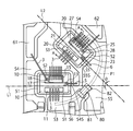
- FIG. 1 is a plan view showing an internal configuration of a semiconductor device 1 according to an embodiment of the present invention. It is a figure which shows the external appearance of the semiconductor device 1 which concerns on embodiment of this invention. It is a circuit diagram of semiconductor device 1 concerning an embodiment of the present invention. It is an enlarged plan view of FIG. FIG. 5 is a cross-sectional view taken along the line AA of FIG. 4;
- the semiconductor device 1 has a first half bridge circuit and a second half bridge circuit.
- the first half bridge circuit includes a high side switching unit composed of cascaded GaN-HEMTs 10 and MOS-FETs 15 and a low side switch unit composed of cascaded GaN-HEMTs 20 and MOS-FETs 25 .
- the second half bridge circuit includes a high side switching unit composed of cascaded GaN-HEMTs 30 and MOS-FETs 35 and a low side switch unit composed of cascaded GaN-HEMTs 40 and MOS-FETs 45 .
- the semiconductor device 1 functions as, for example, a DC / DC converter, a rectifier, and an inverter.
- the bypass capacitor 80 is provided between the terminal T1 and the terminal T7, and the bypass capacitor 90 is provided between the terminal T11 and the terminal T7.
- the bypass capacitor 80 is provided between the drain electrode of the GaN-HEMT 10 and the source electrode of the MOS-FET 25.
- the bypass capacitor 90 is provided between the drain electrode of the GaN-HEMT 30 and the source electrode of the MOS-FET 45.
- the capacitance of the bypass capacitors 80 and 90 is, for example, as large as possible within the range where the breakdown voltage of the bypass capacitors is larger than the breakdown voltage of the GaN-HEMTs 10, 20, 30, and 40.
- the semiconductor device 1 includes an insulating substrate 2, GaN-HEMTs 10, 20, 30, 40 (first, second, third and fourth GaN-HEMTs), and MOS-FETs 15, 25, 35, 45 (first , Second and third MOS-FETs), bypass capacitors 80 and 90, and a resin sealing portion 95.
- the semiconductor device 1 is configured to be symmetrical in the left-right direction, a first half bridge circuit is formed on one side, and a second half bridge circuit is formed on the other side.
- the semiconductor device 1 includes conductive pattern portions 51, 52, 53, 54, 55, 56, 57, 58, 59 (first, second, third, fourth, fifth, etc.) formed on the insulating substrate 2. , Sixth, seventh, eighth and ninth conductive pattern portions) and conductive pattern portions 61, 62, 63, 64.
- the conductive pattern portions 51 to 59 and 61 to 64 are formed, for example, by patterning a copper foil on the insulating substrate 2. Detailed description of each conductive pattern portion will be described later.
- the insulating substrate 2 is made of an insulating material, and is made of, for example, a material such as ceramic with good heat dissipation. As shown in FIG. 1, the insulating substrate 2 has a substrate side 2a (first substrate side) and a substrate side 2b (second substrate side) opposed to the substrate side 2a.
- the substrate sides 2a and 2b are sides from which various terminals of the semiconductor device 1 protrude in plan view. That is, terminals T1, T4, T7, T11 and T14 protrude from substrate side 2a in plan view, and terminals T2, T3, T5, T6, T12, T13, T15 and T16 from substrate side 2b in plan view It is sticking out.
- a conductive pattern portion 65 connected to a heat sink (not shown) such as a heat sink is formed on the back surface of the insulating substrate 2 so as to cover the back surface (see FIG. 5).
- the GaN-HEMTs 10, 20, 30, 40 are high electron mobility transistors using a gallium nitride (GaN) -based semiconductor material.
- the GaN-HEMTs 10, 20, 30, and 40 are transistors of a type in which a channel flows even when the gate voltage is 0 V and in which current flows (so-called normally on type).
- the MOS-FETs 15, 25, 35, 45 are field effect transistors (FETs) having a MOS (Metal Oxide Semiconductor) structure.
- the MOS-FETs 15, 25, 35, 45 are so-called normally-off transistors.
- the bypass capacitor 80 has an electrode 81 and an electrode 82, and the bypass capacitor 90 has an electrode 91 and an electrode 92.
- the bypass capacitors 80 and 90 are resin-sealed by a resin sealing portion 95 together with electronic parts such as the GaN-HEMTs 10, 20, 30, 40, the MOS-FETs 15, 25, 35, 45 and the like.
- the semiconductor device 1 further includes terminals T1, T2, T3, T4, T5, T6, T7, T11, T12, T13, T14, T15, and T16 for connecting to an external device (an IC chip such as a driver, power supply). Have. These terminals are provided so as to project from the paper surface in FIGS. 1 and 2. The portions other than the inner leads of these terminals and the back surface of the insulating substrate 2 are resin-sealed by a resin sealing portion 95. As shown in FIG. 2, the semiconductor device 1 is provided with through holes H1 and H2 for inserting mounting screws.
- the terminals T1 and T11 are terminals (high voltage side terminals) connected to the high voltage side of the power supply (not shown).
- the terminal T7 is a terminal (low voltage side terminal) connected to the low voltage side (ground) of the power supply.
- the terminal T1 and the terminal T11 are connected to the load on the output side.
- Terminals T2 and T12 are terminals for inputting a gate signal to the high side switch of the half bridge circuit.
- the terminal T2 is electrically connected to the gate electrode 18 of the MOS-FET 15, and the terminal T12 is electrically connected to the gate electrode 38 of the MOS-FET 35.
- Terminals T5 and T15 are terminals for inputting a gate signal to the low side switch of the half bridge circuit.
- the terminal T5 is electrically connected to the gate electrode 28 of the MOS-FET 25, and the terminal T15 is electrically connected to the gate electrode 48 of the MOS-FET 45.
- These terminals T2, T5, T12 and T15 are electrically connected to a driver (not shown) for driving the power supply circuit.
- the terminal T3 is a terminal for monitoring the voltage between the MOS-FET 15 and the GaN-HEMT 20.
- the terminal T13 is a terminal for monitoring the voltage between the MOS-FET 35 and the GaN-HEMT 40.
- the terminal T4 is a terminal that outputs the output voltage of the first half bridge circuit.
- the terminal T14 is a terminal that outputs the output voltage of the second half bridge circuit.
- the terminal T6 is a terminal for monitoring the voltage between the MOS-FET 25 and the terminal T7.
- the terminal T16 is a terminal for monitoring the voltage between the MOS-FET 45 and the terminal T7.
- GaN-HEMTs 10, 20, 30, 40 and the MOS-FETs 15, 25, 35, 45 will be described in detail.
- the GaN-HEMTs 10, 20, 30, and 40 are N-type semiconductor devices having a lateral structure, and a drain electrode, a source electrode, and a gate electrode are provided on the top surface.
- the GaN-HEMT 20 includes the drain electrode 21 (third GaN main electrode), the source electrode 22 (fourth GaN main electrode), and the gate electrode 23 (second GaN gate). Electrode).
- the GaN-HEMT 10 has a drain electrode 11 (first GaN main electrode), a source electrode (second GaN main electrode, not shown), and a gate electrode 13 (first GaN gate electrode).
- the GaN-HEMT 30 has a drain electrode 31 (fifth GaN main electrode), a source electrode (sixth GaN main electrode, not shown), and a gate electrode 33 (third GaN gate electrode).
- the GaN-HEMT 40 has a drain electrode 41 (seventh GaN main electrode), a source electrode (eighth GaN main electrode, not shown), and a gate electrode 43 (fourth GaN gate electrode).
- the GaN-HEMTs 10, 20, 30, 40 may have a vertical structure.
- the drain electrode provided on the back surface of GaN-HEMT 10 is connected to conductive pattern portion 51 via solder, and conductive pattern portion 51 and conductive pattern portion 53 are connected and integrated As a conductive pattern portion of
- the drain electrode provided on the back surface of the GaN-HEMT 20 is connected to the conductive pattern portion 52 via the solder, and the conductive pattern portion 52 and the conductive pattern portion 55 are connected.
- the MOS-FETs 15, 25, 35, 45 are N-type semiconductor devices having a vertical structure, a source electrode and a gate electrode are provided on the upper surface, and a drain electrode is provided on the lower surface.
- the MOS-FET 25 includes a drain electrode 26 (third MOS main electrode), a source electrode 27 (fourth MOS main electrode), and a gate electrode 28 (second MOS gate). Electrode).
- the MOS-FET 15 has a drain electrode (first MOS main electrode, not shown), a source electrode 17 (second MOS main electrode) and a gate electrode 18 (first MOS gate electrode).
- the MOS-FET 35 has a drain electrode (fifth MOS main electrode, not shown), a source electrode 37 (sixth MOS main electrode), and a gate electrode 38 (third MOS gate electrode).
- the MOS-FET 45 has a drain electrode (seventh MOS main electrode, not shown), a source electrode 47 (eighth MOS main electrode) and a gate electrode 48 (fourth MOS gate electrode).
- the MOS-FET 25 is disposed on the GaN-HEMT 20 such that the drain electrode 26 of the MOS-FET 25 is electrically connected to the source electrode 22 of the GaN-HEMT 20.
- the MOS-FETs 15, 35, 45 are disposed on the GaN-HEMTs 10, 30, 40, respectively. That is, the drain electrode of the MOS-FET 15 is electrically connected to the source electrode of the GaN-HEMT 10 via solder, and the drain electrode of the MOS-FET 35 is electrically connected to the source electrode of the GaN-HEMT 30 via solder.
- the drain electrode of the MOS-FET 45 is electrically connected to the source electrode of the GaN-HEMT 40 via a solder.
- the drain electrode 11 of the GaN-HEMT 10 is electrically connected to the conductive pattern portion 53 via the metal wire 3.
- the drain electrode 11 is electrically connected to the high voltage side terminal (terminal T1) through the conductive pattern portion 53.
- the source electrode (not shown) of the GaN-HEMT 10 is connected to the drain electrode of the MOS-FET 15 via a solder.
- the gate electrode 13 of the GaN-HEMT 10 is electrically connected to the conductive pattern portion 54 via the metal wire 5.
- the gate electrode 13 is electrically connected to the source electrode 17 of the MOS-FET 15 through the conductive pattern portion 54.
- the drain electrode 21 of the GaN-HEMT 20 is electrically connected to the conductive pattern portion 54 via the metal wire 3.
- the source electrode of the GaN-HEMT 20 is connected to the drain electrode of the MOS-FET 25 via a solder.
- the gate electrode 23 of the GaN-HEMT 20 is electrically connected to the conductive pattern portion 55 via the metal wire 6.
- the gate electrode 23 is electrically connected to the source electrode 27 of the MOS-FET 25 through the conductive pattern portion 55.
- the drain electrode 31 of the GaN-HEMT 30 is electrically connected to the conductive pattern portion 58 via the metal wire 3.
- the source electrode of the GaN-HEMT 20 is connected to the drain electrode of the MOS-FET 35 via a solder.
- the gate electrode 33 of the GaN-HEMT 30 is electrically connected to the conductive pattern portion 59 via the metal wire 7.
- the gate electrode 33 is electrically connected to the source electrode 37 of the MOS-FET 35 through the conductive pattern portion 59.
- the drain electrode 41 of the GaN-HEMT 40 is electrically connected to the conductive pattern portion 59 via the metal wire 3.
- the source electrode of the GaN-HEMT 40 is connected to the drain electrode of the MOS-FET 45 via a solder.
- the gate electrode 43 of the GaN-HEMT 40 is electrically connected to the conductive pattern portion 55 via the metal wire 8.
- the gate electrode 43 is electrically connected to the source electrode 47 of the MOS-FET 45 through the conductive pattern portion 55.
- the source electrode 17 of the MOS-FET 15 is electrically connected to the conductive pattern portion 54 through the metal wire 3.
- the gate electrode 18 of the MOS-FET 15 is electrically connected to the conductive pattern portion 61 via the metal wire 3.
- the source electrode 27 of the MOS-FET 25 is electrically connected to the conductive pattern portion 55 through the metal wire 3.
- the source electrode 27 is electrically connected to the low voltage side terminal (terminal T7) through the conductive pattern portion 55.
- the gate electrode 28 of the MOS-FET 25 is electrically connected to the conductive pattern portion 62 through the metal wire 3.
- the source electrode 37 of the MOS-FET 35 is electrically connected to the conductive pattern portion 59 through the metal wire 3.
- the gate electrode 38 of the MOS-FET 35 is electrically connected to the conductive pattern portion 63 through the metal wire 3.
- the source electrode 47 of the MOS-FET 45 is electrically connected to the conductive pattern portion 55 via the metal wire 3.
- the gate electrode 48 of the MOS-FET 45 is electrically connected to the conductive pattern portion 64 through the metal wire 3.
- the metal wire 3 is an aluminum wire (Al wire), but may be made of another metal material. Although the aluminum wires (Al wires) are used as the metal wires 5, 6, 7, and 8 in this embodiment, other metal materials may be used. The material of the metal wires 5, 6, 7, 8 may be matched to the material of the gate electrodes 13, 23, 33, 43.
- a semiconductor switching part and a conductive pattern part may replace with a metal wire and may use the connector which consists of electroconductive board material.
- the conductive pattern portions 51, 52, 53, 54, 55, 61 and 62 are conductive pattern portions for forming the first half bridge circuit.
- the conductive pattern portions 55, 56, 57, 58, 59, 63, 64 are conductive pattern portions for forming a second half bridge circuit.
- the conductive pattern portion 55 is shared by the first half bridge circuit and the second half bridge circuit. Further, as shown in FIG. 1, the conductive pattern portion 55 is formed in a symmetrical shape in the left-right direction.
- the conductive pattern portion 51 is a conductive pattern portion for mounting the GaN-HEMT 10.
- the conductive pattern portion 52 is a conductive pattern portion for mounting the GaN-HEMT 20.
- the conductive pattern portion 56 is a conductive pattern portion for mounting the GaN-HEMT 30.
- the conductive pattern portion 57 is a conductive pattern portion for mounting the GaN-HEMT 40.
- the conductive pattern portions 51, 52, 56, 57 are formed in a substantially square shape in plan view in accordance with the shapes of the GaN-HEMTs 10, 20, 30, 40.
- the GaN-HEMT 10 is disposed on the conductive pattern portion 51
- the GaN-HEMT 20 is disposed on the conductive pattern portion 52
- the GaN-HEMT 30 is disposed on the conductive pattern portion 56
- the GaN-HEMT 40 is a conductive pattern portion 57.
- the drain electrode 11 of the GaN-HEMT 10 is electrically connected to the conductive pattern portion 53 via the metal wire 3, and the terminal T1 and the electrode 81 of the bypass capacitor 80 are connected via solder.
- the drain electrode 31 of the GaN-HEMT 30 is electrically connected to the conductive pattern portion 58 via the metal wire 3, and the terminal T11 and the electrode 91 of the bypass capacitor 90 are connected via solder. .
- the conductive pattern portion 54 electrically connects the high side switches (GaN-HEMTs 10 and MOS-FETs 15) of the first half bridge circuit to the low side switches (GaN-HEMTs 20 and MOS-FETs 25). Further, the terminals T3 and T4 are electrically connected to the conductive pattern portion 54 through solder. Further, the other end of the metal wire 5 whose one end is connected to the gate electrode 13 of the GaN-HEMT 10 is connected to the conductive pattern portion 54.
- the conductive pattern portion 59 electrically connects the high side switches (GaN-HEMTs 30 and MOS-FETs 35) and the low side switches (GaN-HEMTs 40 and MOS-FETs 45) of the second half bridge circuit. Further, the terminal T13 and the terminal T14 are electrically connected to the conductive pattern portion 59 via a solder. Further, the other end of the metal wire 7 whose one end is connected to the gate electrode 33 of the GaN-HEMT 30 is connected to the conductive pattern portion 59.
- the electrode 82 of the bypass capacitor 80 is electrically connected to the conductive pattern portion 55 via a solder, and the source electrode 27 of the MOS-FET 25 is electrically connected via the metal wire 3. Further, the electrode 92 of the bypass capacitor 90 is electrically connected to the conductive pattern portion 55 via the solder, and the source electrode 47 of the MOS-FET 45 is electrically connected via the metal wire 3. Further, terminals T6, T7 and T16 are electrically connected to the conductive pattern portion 55 through solder.
- the gate electrode 23 of the GaN-HEMT 20 is electrically connected to the conductive pattern portion 55 through the metal wire 6, and the gate electrode 43 of the GaN-HEMT 40 is electrically connected through the metal wire 8. It is connected.
- the conductive pattern portion 61 is a conductive pattern portion for electrically connecting the gate electrode 18 of the MOS-FET 15 and the terminal T2.
- the gate electrode 18 is electrically connected to the conductive pattern portion 61 through the metal wire 3, and the terminal T2 is electrically connected to the conductive pattern portion 61 through the solder.
- the conductive pattern portion 63 is a conductive pattern portion for electrically connecting the gate electrode 38 of the MOS-FET 35 and the terminal T12.
- the gate electrode 38 is electrically connected to the conductive pattern portion 63 through the metal wire 3, and the terminal T12 is electrically connected to the conductive pattern portion 63 through the solder.
- the conductive pattern portion 62 is a conductive pattern portion for electrically connecting the gate electrode 28 of the MOS-FET 25 and the terminal T5.
- the gate electrode 28 is electrically connected to the conductive pattern portion 62 through the metal wire 3, and the terminal T5 is electrically connected to the conductive pattern portion 62 through the solder.
- the conductive pattern portion 64 is a conductive pattern portion for electrically connecting the gate electrode 48 of the MOS-FET 45 and the terminal T15.
- the gate electrode 48 is electrically connected to the conductive pattern portion 64 through the metal wire 3, and the terminal T15 is electrically connected to the conductive pattern portion 64 through the solder.
- the GaN-HEMT 10 and the GaN-HEMT 20 have a substantially rectangular shape in plan view.
- the GaN-HEMT 10 has a side S1 (first side) and a side S2 (second side) opposite to the side S1.
- the side S1 and the side S2 are substantially parallel.
- the GaN-HEMT 20 has a side S3 (third side) and a side S4 (fourth side) opposite to the side S3.
- the side S3 and the side S4 are substantially parallel.
- the drain electrode 11 of the GaN-HEMT 10 is provided along the side S1.
- the source electrode 17 of the MOS-FET 15 is provided along the side S2.
- the drain electrode 21 of the GaN-HEMT 20 is provided along the side S3.
- the source electrode 27 of the MOS-FET 25 is provided along the side S4.
- a virtual line L1 extending along the side S1 intersects with a virtual line L2 extending along the side S3.
- the virtual line L1 and the virtual line L2 are not parallel.
- the bypass capacitor path P1 can be shortened compared to the case where the GaN-HEMT 10 and the GaN-HEMT 20 are arranged in parallel (that is, when the virtual line L1 and the virtual line L2 are parallel). Parasitic inductance can be reduced.
- the angle ⁇ at which the imaginary line L1 and the imaginary line L2 intersect is preferably 30 ° or more and 135 ° or less, and more preferably 30 ° or more and 60 ° or less. In the present embodiment, the angle ⁇ is approximately 45 °.
- the GaN-HEMT 10 on the high side switch side is disposed such that the virtual line L1 is substantially parallel to the substrate side 2a of the insulating substrate 2, and the GaN on the low side switch side
- the HEMT 20 is disposed such that the virtual line L 2 is oblique to the substrate side 2 a of the insulating substrate 2. This facilitates securing of the space in the upper central region of the insulating substrate 2. That is, in the conductive pattern portion 55, the region in which the metal wire 3 connected to the source electrode 27 of the MOS-FET 25 is connected to the conductive pattern portion 55 can be widened. As a result, the parasitic inductance of the bypass capacitor path P1 can be reduced.
- the semiconductor device 1 has a symmetrical configuration. That is, the GaN-HEMT 10 and the GaN-HEMT 20 are disposed symmetrically with the conductive pattern portion 55 interposed therebetween, and the GaN-HEMT 20 and the GaN-HEMT 40 are disposed symmetrically disposed with the conductive pattern portion 55 interposed therebetween.
- the bypass capacitor 80 and the bypass capacitor 90 are also disposed symmetrically with the conductive pattern portion 55 interposed therebetween.
- the conductive pattern portion 55 is shared by two half bridge circuits. By configuring the semiconductor device 1 symmetrically in this manner, the conductive pattern portion 55 can be made wider, and the parasitic inductance of the bypass capacitor paths P1 and P2 can be further reduced.
- the GaN-HEMT 20 has a side S5 (fifth side) connecting the side S3 and the side S4.
- the conductive pattern portion 55 has a conductive pattern side 55S opposed to the side S5.
- the gate electrode 23 of the GaN-HEMT 20 is electrically connected to the conductive pattern portion 55 via the metal wire 6.
- the metal wire 6 is orthogonal to the side S 5 of the GaN-HEMT 20 and the conductive pattern side 55 S of the conductive pattern portion 55.
- the gate electrode 23 is connected to the conductive pattern portion 55 at the shortest distance, and the metal wire 6 can be shortened.
- the term "orthogonal" includes not only the case of strictly crossing at 90 ° but also the case of being substantially orthogonal in order to allow manufacturing tolerances and errors.
- the metal wire 8 electrically connecting the gate electrode 43 of the GaN-HEMT 40 and the conductive pattern portion 55 is also configured to have the shortest length in the same manner as the metal wire 6.
- the gate electrode 23 of the GaN-HEMT 20 is electrically connected to the conductive pattern portion 55 through the connector, and this connector is the side S5 of the GaN-HEMT 20, and It is orthogonal to the conductive pattern side 55S of the conductive pattern portion 55. Therefore, generally speaking, connecting members such as metal wires and connectors are provided orthogonal to the side S5 of the GaN-HEMT 20 and the conductive pattern side 55S of the conductive pattern portion 55.
- the GaN-HEMT 10 and the GaN-HEMT 20 are disposed on the insulating substrate 2 such that the virtual line L1 and the virtual line L2 intersect.
- the bypass capacitor path P1 can be shortened, and the parasitic inductance of the bypass capacitor path P1 can be reduced.
- the metal wire 6 electrically connecting the gate electrode 23 of the GaN-HEMT 20 to the conductive pattern portion 55 is substantially orthogonal to the side S 5 of the GaN-HEMT 20 and the conductive pattern side 55 S of the conductive pattern portion 55.
- the gate electrode 23 of the GaN-HEMT 20 is connected to the conductive pattern portion 55 by the metal wire 6 at the shortest distance.
- the semiconductor device according to the present embodiment has been described above.
- the semiconductor device according to the present invention is not limited to the above-described half bridge circuit, but may be applied to a power supply circuit having another configuration such as a full bridge circuit or a push-pull circuit as long as it has cascaded semiconductor switching elements. It is also possible.
- the gate electrode 13 may be electrically connected to the conductive pattern portion 54 with the metal wire 5, and the metal wire 5 may be provided so as to have the shortest length. That is, as shown in FIG. 4, the metal wire 5 may be provided to be orthogonal to the side S6 connecting the side S1 and the side S2 and the conductive pattern side 54S opposed to the side S6. Thereby, the malfunction of the power supply circuit can be further suppressed.
- Reference Signs List 1 semiconductor device 2 insulating substrate 2a, 2b substrate side 3, 5, 6, 7, 8 metal wire 10, 20, 30, 40 GaN-HEMT 11, 21, 31, 41 drain electrode 22 source electrode 13, 23, 33, 43 gate electrode 15, 25, 35, 45 MOS-FET 26 drain electrode 17, 27, 37, 47 source electrode 18, 28, 38, 48 gate electrode 51, 52, 53, 54, 55, 56, 57, 58, 59, 61, 62, 63, 64, 65 conductive pattern Portions 54S, 55S Conductive pattern sides 80, 90 Bypass capacitors 81, 82, 91, 92 Electrodes 95 Resin sealing portions H1, H2 Through holes L1, L2 Virtual lines N1, N2, N3, N4 Nodes S1, S2, S3, S4 , S5, S6 Sides T1, T2, T3, T4, T5, T6, T7, T11, T12, T13, T14, T15, T16 Terminals
Landscapes
- Engineering & Computer Science (AREA)
- Power Engineering (AREA)
- Junction Field-Effect Transistors (AREA)
- Physics & Mathematics (AREA)
- Geometry (AREA)
Abstract
【課題】GaN-HEMTを有する電源回路の誤動作を抑制する。 【解決手段】実施形態の半導体装置1は、絶縁基板2と、前記絶縁基板の上に形成された導電パターン部51,52,53,54,55と、導電パターン部51の上に配置されたGaN-HEMT10と、導電パターン部52の上に配置されたGaN-HEMT20と、を備え、GaN-HEMT10の仮想線L1およびGaN-HEMT20の仮想線L2が交わり、GaN-HEMT20のGaNゲート電極23は金属ワイヤー6を介して導電パターン部55に電気的に接続され、金属ワイヤー6はGaN-HEMT20の辺S5および導電パターン部55の導電パターン辺55Sに対して直交する。
Description
本発明は、電源回路を有する半導体装置に関する。
電源電圧を所望の電圧に変換して出力する電源回路を有する半導体装置が知られている。電源回路には、インバータ、整流器、DC/DCコンバータなどがある。このような半導体装置は、例えば、太陽光発電システムのパワーコンディショナやサーバ装置等に用いられる。半導体装置内の電源回路では、ハーフブリッジ回路やフルブリッジ回路が用いられる。これらの回路は、半導体スイッチング素子が縦続接続された構造を有する。
近年、電源回路の電力変換効率を高めるべく、高速動作(例えば100MHz超)が可能なGaN系半導体材料を用いた高電子移動度トランジスタ(High Electron Mobility Transistor:HEMT)(以下、単に「GaN-HEMT」ともいう。)をスイッチング素子に適用することが検討されている。
なお、特許文献1には、GaN-HEMTを用いたLED駆動装置が記載されている。
GaN-HEMTを電源回路に適用する場合、高速動作に伴って、電源回路の配線における寄生インダクタンスの影響が従来よりも格段に大きくなる。このため、電源回路の誤動作が引き起こされるおそれがある。
そこで、本発明は、GaN-HEMTを有する電源回路の誤動作を抑制することができる半導体装置を提供することを目的とする。
本発明に係る半導体装置は、
絶縁基板と、
前記絶縁基板の上に形成された第1の導電パターン部と、
前記絶縁基板の上に形成された第2の導電パターン部と、
前記絶縁基板の上に形成された第3の導電パターン部と、
前記絶縁基板の上に形成された第4の導電パターン部と、
前記絶縁基板の上に形成された第5の導電パターン部と、
第1のGaN主電極、第2のGaN主電極および第1のGaNゲート電極を有し、前記第1の導電パターン部の上に配置された第1のGaN-HEMTと、
第1のMOS主電極、第2のMOS主電極および第1のMOSゲート電極を有し、前記第1のMOS主電極が前記第2のGaN主電極に電気的に接続された第1のMOS-FETと、
第3のGaN主電極、第4のGaN主電極および第2のGaNゲート電極を有し、前記第2の導電パターン部の上に配置された第2のGaN-HEMTと、
第3のMOS主電極、第4のMOS主電極および第2のMOSゲート電極を有し、前記第3のMOS主電極が前記第4のGaN主電極に電気的に接続された第2のMOS-FETと、
第1の電極および第2の電極を有するバイパスコンデンサと、を備え、
前記第1のGaN-HEMTの前記第1のGaN主電極は、前記第3の導電パターン部に電気的に接続され、前記第1のMOS-FETの前記第2のMOS主電極は、前記第4の導電パターン部に電気的に接続され、前記第2のGaN-HEMTの前記第3のGaN主電極は、前記第4の導電パターン部に電気的に接続され、前記第2のMOS-FETの前記第4のMOS主電極は、前記第5の導電パターン部に電気的に接続され、前記バイパスコンデンサの前記第1の電極は、前記第3の導電パターン部に電気的に接続され、前記第2の電極は、前記第5の導電パターン部に電気的に接続され、
前記第1のGaN-HEMTは、第1の辺と、前記第1の辺に対向する第2の辺とを有し、前記第2のGaN-HEMTは、第3の辺と、前記第3の辺に対向する第4の辺とを有し、
前記第1のGaN-HEMTの前記第1のGaN主電極は、前記第1の辺に沿って設けられ、前記第2のGaN-HEMTの前記第3のGaN主電極は、前記第3の辺に沿って設けられ、前記第1の辺に沿って延びる第1の仮想線と、前記第3の辺に沿って延びる第2の仮想線とが交わり、
前記第2のGaN-HEMTは、前記第3の辺と前記第4の辺を接続する第5の辺を有し、前記第5の導電パターン部は、前記第5の辺に対向する導電パターン辺を有し、
前記第2のGaN-HEMTの前記第2のGaNゲート電極は、接続部材を介して前記第5の導電パターン部に電気的に接続され、前記接続部材は、前記第5の辺および前記導電パターン辺に対して直交することを特徴とする。
また、前記半導体装置において、
前記第1のGaN-HEMTおよび前記第2のGaN-HEMTは、ノーマリーオン型のトランジスタであり、前記第1のMOS-FETおよび前記第2のMOS-FETは、ノーマリーオフ型のトランジスタであるようにしてもよい。
前記第1のGaN-HEMTおよび前記第2のGaN-HEMTは、ノーマリーオン型のトランジスタであり、前記第1のMOS-FETおよび前記第2のMOS-FETは、ノーマリーオフ型のトランジスタであるようにしてもよい。
また、前記半導体装置において、
前記接続部材は、金属ワイヤーまたは接続子であるようにしてもよい。
前記接続部材は、金属ワイヤーまたは接続子であるようにしてもよい。
また、前記半導体装置において、
前記第1のGaN-HEMTの前記第1のGaN主電極は、前記第3の導電パターン部を介して高電圧側端子に電気的に接続され、前記第2のMOS-FETの前記第4のMOS主電極は、前記第5の導電パターン部を介して低電圧側端子に電気的に接続されているようにしてもよい。
前記第1のGaN-HEMTの前記第1のGaN主電極は、前記第3の導電パターン部を介して高電圧側端子に電気的に接続され、前記第2のMOS-FETの前記第4のMOS主電極は、前記第5の導電パターン部を介して低電圧側端子に電気的に接続されているようにしてもよい。
また、前記半導体装置において、
前記絶縁基板は、平面視して前記高電圧側端子と前記低電圧側端子が突き出る第1の基板辺と、前記第1の基板辺に対向する第2の基板辺とを有し、
前記第1のGaN-HEMTは、前記第1の仮想線が前記第1の基板辺に対して平行になるように配置され、前記第2のGaN-HEMTは、前記第2の仮想線が前記第1の基板辺に対して斜めになるように配置されているようにしてもよい。
前記絶縁基板は、平面視して前記高電圧側端子と前記低電圧側端子が突き出る第1の基板辺と、前記第1の基板辺に対向する第2の基板辺とを有し、
前記第1のGaN-HEMTは、前記第1の仮想線が前記第1の基板辺に対して平行になるように配置され、前記第2のGaN-HEMTは、前記第2の仮想線が前記第1の基板辺に対して斜めになるように配置されているようにしてもよい。
また、前記半導体装置において、
前記第1の仮想線と前記第2の仮想線が交わる角度は、30°以上、60°以下であるようにしてもよい。
前記第1の仮想線と前記第2の仮想線が交わる角度は、30°以上、60°以下であるようにしてもよい。
また、前記半導体装置において、
前記第1の仮想線と前記第2の仮想線が交わる角度は、45°であるようにしてもよい。
前記第1の仮想線と前記第2の仮想線が交わる角度は、45°であるようにしてもよい。
また、前記半導体装置において、
前記第1のGaN-HEMTは、前記第1の辺と前記第2の辺を接続する第6の辺を有し、前記第4の導電パターン部は、前記第6の辺に対向する導電パターン辺を有し、
前記第1のGaN-HEMTの前記第1のGaNゲート電極は、接続部材を介して前記第4の導電パターン部に電気的に接続され、前記接続部材は、前記第6の辺および前記導電パターン辺に対して直交するようにしてもよい。
前記第1のGaN-HEMTは、前記第1の辺と前記第2の辺を接続する第6の辺を有し、前記第4の導電パターン部は、前記第6の辺に対向する導電パターン辺を有し、
前記第1のGaN-HEMTの前記第1のGaNゲート電極は、接続部材を介して前記第4の導電パターン部に電気的に接続され、前記接続部材は、前記第6の辺および前記導電パターン辺に対して直交するようにしてもよい。
また、前記半導体装置において、
前記第1のMOS-FETは前記第1のGaN-HEMTの上に配置され、前記第2のMOS-FETは前記第2のGaN-HEMTの上に配置されているようにしてもよい。
前記第1のMOS-FETは前記第1のGaN-HEMTの上に配置され、前記第2のMOS-FETは前記第2のGaN-HEMTの上に配置されているようにしてもよい。
また、前記半導体装置において、
前記バイパスコンデンサは、前記第1のGaN-HEMT、前記第2のGaN-HEMT、前記第1のMOS-FETおよび前記第2のMOS-FETとともに樹脂封止されているようにしてもよい。
前記バイパスコンデンサは、前記第1のGaN-HEMT、前記第2のGaN-HEMT、前記第1のMOS-FETおよび前記第2のMOS-FETとともに樹脂封止されているようにしてもよい。
また、前記半導体装置において、
前記絶縁基板の上に形成された第6の導電パターン部と、
前記絶縁基板の上に形成された第7の導電パターン部と、
前記絶縁基板の上に形成された第8の導電パターン部と、
前記絶縁基板の上に形成された第9の導電パターン部と、
第5のGaN主電極、第6のGaN主電極および第3のGaNゲート電極を有し、前記第6の導電パターン部の上に配置された第3のGaN-HEMTと、
第5のMOS主電極、第6のMOS主電極および第3のMOSゲート電極を有し、前記第5のMOS主電極が前記第6のGaN主電極に電気的に接続された第3のMOS-FETと、
第7のGaN主電極、第8のGaN主電極および第4のGaNゲート電極を有し、前記第7の導電パターン部の上に配置された第4のGaN-HEMTと、
第7のMOS主電極、第8のMOS主電極および第4のMOSゲート電極を有し、前記第7のMOS主電極が前記第8のGaN主電極に電気的に接続された第4のMOS-FETと、
前記第3のGaN-HEMTの前記第5のGaN主電極は、前記第8の導電パターン部に電気的に接続され、前記第3のMOS-FETの前記第6のMOS主電極は、前記第9の導電パターン部に電気的に接続され、前記第4のGaN-HEMTの前記第7のGaN主電極は、前記第9の導電パターン部に電気的に接続され、前記第4のMOS-FETの前記第8のMOS主電極は、前記第5の導電パターン部に電気的に接続され、
前記第1のGaN-HEMTと前記第3のGaN-HEMTは、前記第5の導電パターン部を挟んで対称に配置され、前記第2のGaN-HEMTと前記第4のGaN-HEMTは、前記第5の導電パターン部を挟んで対称に配置されているようにしてもよい。
また、前記半導体装置において、
第3の電極および第4の電極を有する別のバイパスコンデンサをさらに備え、
前記第3の電極は前記第8の導電パターン部に電気的に接続され、前記第4の電極は前記第5の導電パターン部に電気的に接続され、
前記バイパスコンデンサと前記別のバイパスコンデンサは、前記第5の導電パターン部を挟んで対称に配置されているようにしてもよい。
第3の電極および第4の電極を有する別のバイパスコンデンサをさらに備え、
前記第3の電極は前記第8の導電パターン部に電気的に接続され、前記第4の電極は前記第5の導電パターン部に電気的に接続され、
前記バイパスコンデンサと前記別のバイパスコンデンサは、前記第5の導電パターン部を挟んで対称に配置されているようにしてもよい。
本発明に係る半導体装置では、第1のGaN-HEMTの第1の辺に沿って延びる第1の仮想線と、第2のGaN-HEMTの第3の辺に沿って延びる第2の仮想線とが交わる。これにより、バイパスコンデンサ経路を短くすることができ、バイパスコンデンサ経路の寄生インダクタンスを低減することができる。これに加えて、本発明に係る半導体装置では、第2のGaN-HEMTの第2のGaNゲート電極と第5の導電パターン部とを電気的に接続する金属ワイヤーは、第2のGaN-HEMTの第5の辺および第5の導電パターン部の導電パターン辺に対して直交する。これにより、第2のGaNゲート電極が第5の導電パターン部に最短距離で接続され、当該金属ワイヤーを短くすることができる。よって、本発明によれば、GaN-HEMTを有する電源回路の誤動作を抑制することができる。
以下、図面を参照しつつ本発明の実施形態に係る半導体装置について説明する。なお、各図において同等の機能を有する構成要素には同一の符号を付す。
まず、本発明の実施形態に係る半導体装置1の回路構成について、図3を参照して説明する。図3に示すように、半導体装置1は、第1のハーフブリッジ回路および第2のハーフブリッジ回路を有する。第1のハーフブリッジ回路は、縦続接続されたGaN-HEMT10およびMOS-FET15から構成されるハイサイドスイッチング部と、縦続接続されたGaN-HEMT20およびMOS-FET25から構成されるローサイドスイッチ部とを含む。第2のハーフブリッジ回路は、縦続接続されたGaN-HEMT30およびMOS-FET35から構成されるハイサイドスイッチング部と、縦続接続されたGaN-HEMT40およびMOS-FET45から構成されるローサイドスイッチ部とを含む。半導体装置1は、例えばDC/DCコンバータ、整流器、インバータとして機能する。
図3に示すように、バイパスコンデンサ80は端子T1と端子T7との間に設けられ、バイパスコンデンサ90は端子T11と端子T7との間に設けられている。バイパスコンデンサ80は、GaN-HEMT10のドレイン電極とMOS-FET25のソース電極との間に設けられている。バイパスコンデンサ90は、GaN-HEMT30のドレイン電極とMOS-FET45のソース電極との間に設けられている。このようにバイパスコンデンサ80,90が設けられることで、ノードN1からバイパスコンデンサ80を経てノードN2に至る経路(バイパスコンデンサ経路P1)と、ノードN3からバイパスコンデンサ90を経てノードN4に至る経路(バイパスコンデンサ経路P2)とが形成されている。バイパスコンデンサ80,90は、半導体装置1の電源電圧の変動を回避したり、各種ノイズを除去するために設けられている。
なお、バイパスコンデンサ80,90の静電容量は、例えば、当該バイパスコンデンサの耐圧がGaN-HEMT10,20,30,40の耐圧よりも大きい範囲内で、できるだけ大きい値とする。
次に、半導体装置1の具体的構成について、図1および図2を参照して説明する。
半導体装置1は、絶縁基板2と、GaN-HEMT10,20,30,40(第1、第2、第3および第4のGaN-HEMT)と、MOS-FET15,25,35,45(第1、第2、第3および第4のMOS-FET)と、バイパスコンデンサ80,90と、樹脂封止部95と、を備えている。図1に示すように、半導体装置1は、左右対称に構成されており、一方の側に第1のハーフブリッジ回路が形成され、他方の側に第2のハーフブリッジ回路が形成されている。
また、半導体装置1は、絶縁基板2上に形成された導電パターン部51,52,53,54,55,56,57,58,59(第1、第2、第3、第4、第5、第6、第7、第8および第9の導電パターン部)と、導電パターン部61,62,63,64と、をさらに備えている。導電パターン部51~59,61~64は、例えば、絶縁基板2上の銅箔をパターニングすることにより形成されたものである。各導電パターン部の詳しい説明は後述する。
絶縁基板2は、絶縁材料からなり、例えば、放熱性の良いセラミック等の材料からなる。図1に示すように、絶縁基板2は、基板辺2a(第1の基板辺)と、この基板辺2aに対向する基板辺2b(第2の基板辺)を有する。基板辺2a,2bは、平面視して半導体装置1の各種端子が突き出る辺である。すなわち、端子T1,T4,T7,T11,T14は平面視して基板辺2aから突き出ており、端子T2,T3,T5,T6,T12,T13,T15,T16は平面視して基板辺2bから突き出ている。なお、絶縁基板2の裏面には、ヒートシンク等の放熱体(図示せず)に接続される導電パターン部65が裏面を被覆するように形成されている(図5参照)。
GaN-HEMT10,20,30,40は、窒化ガリウム(GaN)系の半導体材料を用いた高電子移動度トランジスタである。GaN-HEMT10,20,30,40は、ゲート電圧が0Vの場合でもチャネルが存在し、電流が流れるタイプ(いわゆるノーマリーオン型)のトランジスタである。
MOS-FET15,25,35,45は、MOS(Metal Oxide Semiconductor)構造を有する電界効果トランジスタ(Field Effect Transistor:FET)である。MOS-FET15,25,35,45は、いわゆるノーマリーオフ型のトランジスタである。
図1に示すように、バイパスコンデンサ80は電極81および電極82を有し、バイパスコンデンサ90は電極91および電極92を有する。バイパスコンデンサ80,90は、GaN-HEMT10,20,30,40、MOS-FET15,25,35,45等の電子部品とともに樹脂封止部95により樹脂封止されている。
半導体装置1は、外部の装置(ドライバ等のICチップ、電源)と接続するための端子T1,T2,T3,T4,T5,T6,T7,T11,T12,T13,T14,T15,T16をさらに備えている。これらの端子は、図1および図2において紙面から手前に飛び出すように設けられている。これらの端子のインナーリードおよび絶縁基板2の裏面以外の部分は、樹脂封止部95により樹脂封止されている。なお、図2に示すように、半導体装置1には、取り付け用のネジを挿通させるための貫通孔H1,H2が設けられている。
ここで、半導体装置1の各端子の詳細について説明する。
端子T1,T11は、電源(図示せず)の高電圧側に接続される端子(高電圧側端子)である。一方、端子T7は、電源の低電圧側(グランド)に接続される端子(低電圧側端子)である。なお、半導体装置1の電源回路が整流器として機能する場合、端子T1および端子T11は出力側の負荷に接続される。
端子T2,T12は、ハーフブリッジ回路のハイサイドスイッチに対するゲート信号を入力する端子である。端子T2はMOS-FET15のゲート電極18に電気的に接続され、端子T12はMOS-FET35のゲート電極38に電気的に接続される。端子T5,T15は、ハーフブリッジ回路のローサイドスイッチに対するゲート信号を入力する端子である。端子T5はMOS-FET25のゲート電極28に電気的に接続され、端子T15はMOS-FET45のゲート電極48に電気的に接続される。これらの端子T2,T5,T12,T15は、電源回路を駆動するドライバ(図示せず)に電気的に接続される。
端子T3は、MOS-FET15とGaN-HEMT20間の電圧をモニタするための端子である。同様に、端子T13は、MOS-FET35とGaN-HEMT40間の電圧をモニタするための端子である。端子T4は、第1のハーフブリッジ回路の出力電圧を出力する端子である。同様に、端子T14は、第2のハーフブリッジ回路の出力電圧を出力する端子である。なお、半導体装置1の電源回路が整流器として機能する場合、端子T4と端子T14の間には入力側の交流電源が接続される。
端子T6は、MOS-FET25と端子T7間の電圧をモニタするための端子である。同様に、端子T16は、MOS-FET45と端子T7間の電圧をモニタするための端子である。
次に、GaN-HEMT10,20,30,40、およびMOS-FET15,25,35,45について詳しく説明する。
GaN-HEMT10,20,30,40は、横型構造を有するN型の半導体デバイスであり、上面にドレイン電極、ソース電極およびゲート電極が設けられている。例えば、GaN-HEMT20は、図4および図5に示すように、ドレイン電極21(第3のGaN主電極)、ソース電極22(第4のGaN主電極)およびゲート電極23(第2のGaNゲート電極)を有する。同様に、GaN-HEMT10は、ドレイン電極11(第1のGaN主電極)、ソース電極(第2のGaN主電極、図示せず)、およびゲート電極13(第1のGaNゲート電極)を有する。GaN-HEMT30は、ドレイン電極31(第5のGaN主電極)、ソース電極(第6のGaN主電極、図示せず)、およびゲート電極33(第3のGaNゲート電極)を有する。GaN-HEMT40は、ドレイン電極41(第7のGaN主電極)、ソース電極(第8のGaN主電極、図示せず)、およびゲート電極43(第4のGaNゲート電極)を有する。
なお、GaN-HEMT10,20,30,40は、縦型構造であってもよい。この場合、GaN-HEMT10を例に言えば、GaN-HEMT10の裏面に設けられたドレイン電極がはんだを介して導電パターン部51に接続され、導電パターン部51と導電パターン部53は連結され、一体の導電パターン部として構成される。GaN-HEMT20の場合も同様に、GaN-HEMT20の裏面に設けられたドレイン電極がはんだを介して導電パターン部52に接続され、導電パターン部52と導電パターン部55が連結される。
MOS-FET15,25,35,45は、縦型構造を有するN型の半導体デバイスであり、上面にソース電極およびゲート電極が設けられ、下面にドレイン電極が設けられている。例えば、MOS-FET25は、図4および図5に示すように、ドレイン電極26(第3のMOS主電極)、ソース電極27(第4のMOS主電極)およびゲート電極28(第2のMOSゲート電極)を有する。同様に、MOS-FET15は、ドレイン電極(第1のMOS主電極、図示せず)、ソース電極17(第2のMOS主電極)およびゲート電極18(第1のMOSゲート電極)を有する。MOS-FET35は、ドレイン電極(第5のMOS主電極、図示せず)、ソース電極37(第6のMOS主電極)およびゲート電極38(第3のMOSゲート電極)を有する。MOS-FET45は、ドレイン電極(第7のMOS主電極、図示せず)、ソース電極47(第8のMOS主電極)およびゲート電極48(第4のMOSゲート電極)を有する。
図5に示すように、MOS-FET25のドレイン電極26がGaN-HEMT20のソース電極22に電気的に接続されるように、MOS-FET25はGaN-HEMT20の上に配置されている。MOS-FET25と同様に、MOS-FET15,35,45はそれぞれ、GaN-HEMT10,30,40の上に配置されている。すなわち、MOS-FET15のドレイン電極はGaN-HEMT10のソース電極にはんだを介して電気的に接続され、MOS-FET35のドレイン電極はGaN-HEMT30のソース電極にはんだを介して電気的に接続され、MOS-FET45のドレイン電極はGaN-HEMT40のソース電極にはんだを介して電気的に接続されている。
GaN-HEMT10のドレイン電極11は、金属ワイヤー3を介して導電パターン部53に電気的に接続されている。そして、ドレイン電極11は、導電パターン部53を介して高電圧側端子(端子T1)に電気的に接続されている。GaN-HEMT10のソース電極(図示せず)は、MOS-FET15のドレイン電極にはんだを介して接続されている。GaN-HEMT10のゲート電極13は、金属ワイヤー5を介して導電パターン部54に電気的に接続されている。そして、このゲート電極13は、導電パターン部54を介してMOS-FET15のソース電極17に電気的に接続されている。
GaN-HEMT20のドレイン電極21は、金属ワイヤー3を介して導電パターン部54に電気的に接続されている。GaN-HEMT20のソース電極は、MOS-FET25のドレイン電極にはんだを介して接続されている。GaN-HEMT20のゲート電極23は、金属ワイヤー6を介して導電パターン部55に電気的に接続されている。そして、このゲート電極23は、導電パターン部55を介してMOS-FET25のソース電極27に電気的に接続されている。
GaN-HEMT30のドレイン電極31は、金属ワイヤー3を介して導電パターン部58に電気的に接続されている。GaN-HEMT20のソース電極は、MOS-FET35のドレイン電極にはんだを介して接続されている。GaN-HEMT30のゲート電極33は、金属ワイヤー7を介して導電パターン部59に電気的に接続されている。そして、ゲート電極33は、導電パターン部59を介してMOS-FET35のソース電極37に電気的に接続されている。
GaN-HEMT40のドレイン電極41は、金属ワイヤー3を介して導電パターン部59に電気的に接続されている。GaN-HEMT40のソース電極は、MOS-FET45のドレイン電極にはんだを介して接続されている。GaN-HEMT40のゲート電極43は、金属ワイヤー8を介して導電パターン部55に電気的に接続されている。そして、ゲート電極43は、導電パターン部55を介してMOS-FET45のソース電極47に電気的に接続されている。
MOS-FET15のソース電極17は、金属ワイヤー3を介して導電パターン部54に電気的に接続されている。MOS-FET15のゲート電極18は、金属ワイヤー3を介して導電パターン部61に電気的に接続されている。
MOS-FET25のソース電極27は、金属ワイヤー3を介して導電パターン部55に電気的に接続されている。このソース電極27は、導電パターン部55を介して低電圧側端子(端子T7)に電気的に接続されている。MOS-FET25のゲート電極28は、金属ワイヤー3を介して導電パターン部62に電気的に接続されている。
MOS-FET35のソース電極37は、金属ワイヤー3を介して導電パターン部59に電気的に接続されている。MOS-FET35のゲート電極38は、金属ワイヤー3を介して導電パターン部63に電気的に接続されている。
MOS-FET45のソース電極47は、金属ワイヤー3を介して導電パターン部55に電気的に接続されている。MOS-FET45のゲート電極48は、金属ワイヤー3を介して導電パターン部64に電気的に接続されている。
なお、金属ワイヤー3は、アルミニウム線(Al線)であるが、他の金属材料からなるものであってもよい。金属ワイヤー5,6,7,8についても、本実施形態では、アルミニウム線(Al線)としているが、他の金属材料からなるものを用いてもよい。金属ワイヤー5,6,7,8の材料は、ゲート電極13,23,33,43の材料に合わせてもよい。
なお、半導体スイッチング部と導電パターン部とを電気的に接続するために、金属ワイヤーに代えて、導電性の板材からなる接続子を用いてもよい。
次に、図1を参照して、半導体装置1の各導電パターン部について詳しく説明する。
導電パターン部51,52,53,54,55,61,62は、第1のハーフブリッジ回路を構成するための導電パターン部である。導電パターン部55,56,57,58,59,63,64は、第2のハーフブリッジ回路を構成するための導電パターン部である。導電パターン部55は、第1のハーフブリッジ回路と第2のハーフブリッジ回路に共用される。また、図1に示すように、導電パターン部55は左右対称な形状に形成されている。
導電パターン部51は、GaN-HEMT10を実装するための導電パターン部である。同様に、導電パターン部52は、GaN-HEMT20を実装するための導電パターン部である。導電パターン部56は、GaN-HEMT30を実装するための導電パターン部である。導電パターン部57は、GaN-HEMT40を実装するための導電パターン部である。
本実施形態では、導電パターン部51,52,56,57は、図1に示すように、GaN-HEMT10,20,30,40の形状に合わせて平面視で略四角形状に形成されている。GaN-HEMT10は導電パターン部51の上に配置され、GaN-HEMT20は導電パターン部52の上に配置され、GaN-HEMT30は導電パターン部56の上に配置され、GaN-HEMT40は導電パターン部57の上に配置されている。
導電パターン部53には、GaN-HEMT10のドレイン電極11が金属ワイヤー3を介して電気的に接続されるとともに、端子T1およびバイパスコンデンサ80の電極81がはんだを介して接続されている。同様に、導電パターン部58には、GaN-HEMT30のドレイン電極31が金属ワイヤー3を介して電気的に接続されるとともに、端子T11およびバイパスコンデンサ90の電極91がはんだを介して接続されている。
導電パターン部54は、第1のハーフブリッジ回路のハイサイドスイッチ(GaN-HEMT10とMOS-FET15)とローサイドスイッチ(GaN-HEMT20とMOS-FET25)を電気的に接続する。また、導電パターン部54には、端子T3およびT4がはんだを介して電気的に接続されている。また、導電パターン部54には、GaN-HEMT10のゲート電極13に一端が接続された金属ワイヤー5の他端が接続されている。
同様に、導電パターン部59は、第2のハーフブリッジ回路のハイサイドスイッチ(GaN-HEMT30とMOS-FET35)とローサイドスイッチ(GaN-HEMT40とMOS-FET45)を電気的に接続する。また、導電パターン部59には、端子T13および端子T14がはんだを介して電気的に接続されている。また、導電パターン部59には、GaN-HEMT30のゲート電極33に一端が接続された金属ワイヤー7の他端が接続されている。
導電パターン部55には、バイパスコンデンサ80の電極82がはんだを介して電気的に接続され、MOS-FET25のソース電極27が金属ワイヤー3を介して電気的に接続される。さらに、導電パターン部55には、バイパスコンデンサ90の電極92がはんだを介して電気的に接続され、MOS-FET45のソース電極47が金属ワイヤー3を介して電気的に接続される。また、導電パターン部55には、端子T6,T7およびT16がはんだを介して電気的に接続されている。
図1に示すように、導電パターン部55には、GaN-HEMT20のゲート電極23が金属ワイヤー6を介して電気的に接続され、GaN-HEMT40のゲート電極43が金属ワイヤー8介して電気的に接続されている。
導電パターン部61は、MOS-FET15のゲート電極18と端子T2を電気的に接続するための導電パターン部である。この導電パターン部61には、ゲート電極18が金属ワイヤー3を介して電気的に接続されるとともに、端子T2がはんだを介して電気的に接続される。同様に、導電パターン部63は、MOS-FET35のゲート電極38と端子T12を電気的に接続するための導電パターン部である。この導電パターン部63には、ゲート電極38が金属ワイヤー3を介して電気的に接続されるとともに、端子T12がはんだを介して電気的に接続される。
導電パターン部62は、MOS-FET25のゲート電極28と端子T5を電気的に接続するための導電パターン部である。この導電パターン部62には、ゲート電極28が金属ワイヤー3を介して電気的に接続されるとともに、端子T5がはんだを介して電気的に接続される。同様に、導電パターン部64は、MOS-FET45のゲート電極48と端子T15を電気的に接続するための導電パターン部である。この導電パターン部64には、ゲート電極48が金属ワイヤー3を介して電気的に接続されるとともに、端子T15がはんだを介して電気的に接続される。
次に、GaN-HEMT10とGaN-HEMT20の配置関係について説明する。
図4に示すように、GaN-HEMT10およびGaN-HEMT20は、平面視して略四角形状である。GaN-HEMT10は、辺S1(第1の辺)と、この辺S1に対向する辺S2(第2の辺)を有する。本実施形態では、辺S1と辺S2は略平行である。同様に、GaN-HEMT20は、辺S3(第3の辺)と、この辺S3に対向する辺S4(第4の辺)を有する。本実施形態では、辺S3と辺S4は略平行である。
GaN-HEMT10のドレイン電極11は辺S1に沿って設けられている。また、MOS-FET15のソース電極17は辺S2に沿って設けられている。GaN-HEMT20のドレイン電極21は辺S3に沿って設けられている。また、MOS-FET25のソース電極27は辺S4に沿って設けられている。
半導体装置1においては、図4に示すように、辺S1に沿って延びる仮想線L1と、辺S3に沿って延びる仮想線L2とが交わる。換言すれば、仮想線L1と仮想線L2は平行ではない。これにより、GaN-HEMT10とGaN-HEMT20が平行配置される場合(すなわち、仮想線L1と仮想線L2が平行の場合)に比べてバイパスコンデンサ経路P1を短くすることができ、バイパスコンデンサ経路P1の寄生インダクタンスを低減することができる。
なお、仮想線L1と仮想線L2が交わる角度θが大きいほどバイパスコンデンサ経路P1の長さが短くなり、寄生インダクタンスが抑制される。しかしながら、一方で、MOS-FET15のソース電極17およびGaN-HEMT20のドレイン電極21間の経路の長さが長くなるため、当該経路の寄生インダクタンスが大きくなってしまい、電源回路の誤動作の原因となる。このような事情を考慮すると、仮想線L1と仮想線L2が交わる角度θは、30°以上、135°以下であることが好ましく、30°以上、60°以下であることがさらに好ましい。本実施形態では、角度θは略45°である。
本実施形態では、図1に示すように、ハイサイドスイッチ側のGaN-HEMT10は、仮想線L1が絶縁基板2の基板辺2aに対して略平行になるように配置され、ローサイドスイッチ側のGaN-HEMT20は、仮想線L2が絶縁基板2の基板辺2aに対して斜めになるように配置されている。これにより、絶縁基板2の上側中央領域におけるスペースの確保が容易となる。すなわち、導電パターン部55のうち、MOS-FET25のソース電極27に接続された金属ワイヤー3が導電パターン部55に接続される領域の幅広化を図ることができる。その結果、バイパスコンデンサ経路P1の寄生インダクタンスを低減することができる。
なお、本実施形態では、図1に示すように、半導体装置1は左右対称の構成を有している。すなわち、GaN-HEMT10とGaN-HEMT20は、導電パターン部55を挟んで対称に配置され、GaN-HEMT20とGaN-HEMT40は、導電パターン部55を挟んで対称に配置されている。バイパスコンデンサ80とバイパスコンデンサ90も、導電パターン部55を挟んで対称に配置されている。そして、導電パターン部55が2つのハーフブリッジ回路で共用されている。このように半導体装置1が左右対称に構成されることで、導電パターン部55を幅広とすることができ、バイパスコンデンサ経路P1,P2の寄生インダクタンスをさらに低減することができる。
図4に示すように、GaN-HEMT20は、辺S3と辺S4を接続する辺S5(第5の辺)を有する。導電パターン部55は、辺S5に対向する導電パターン辺55Sを有する。
図4に示すように、GaN-HEMT20のゲート電極23は、金属ワイヤー6を介して導電パターン部55に電気的に接続されている。金属ワイヤー6は、GaN-HEMT20の辺S5、および導電パターン部55の導電パターン辺55Sに対して直交している。これにより、ゲート電極23が導電パターン部55に最短距離で接続され、金属ワイヤー6を短くすることができる。なお、本願において、「直交」の用語は、厳密に90°で交わる場合だけでなく、製造上の公差や誤差を許容する趣旨で、実質的に直交する場合も含む。
本実施形態では、GaN-HEMT40のゲート電極43と導電パターン部55を電気的に接続する金属ワイヤー8についても、金属ワイヤー6と同様にして、長さが最短になるように構成されている。
なお、金属ワイヤー5,6,7,8に代えて、接続子を用いる場合も同様である。例えば金属ワイヤー6に代えて接続子を用いる場合、GaN-HEMT20のゲート電極23は、接続子を介して導電パターン部55に電気的に接続され、この接続子はGaN-HEMT20の辺S5、および導電パターン部55の導電パターン辺55Sに対して直交する。したがって、一般的に言えば、金属ワイヤーや接続子等の接続部材は、GaN-HEMT20の辺S5、および導電パターン部55の導電パターン辺55Sに対して直交するように設けられる。
以上説明したように、本実施形態の半導体装置1においては、GaN-HEMT10とGaN-HEMT20は仮想線L1と仮想線L2が交わるように絶縁基板2上に配置される。これにより、バイパスコンデンサ経路P1を短くすることができ、バイパスコンデンサ経路P1の寄生インダクタンスを低減することができる。さらに、半導体装置1では、GaN-HEMT20のゲート電極23と導電パターン部55を電気的に接続する金属ワイヤー6がGaN-HEMT20の辺S5および導電パターン部55の導電パターン辺55Sに略直交する。これにより、GaN-HEMT20のゲート電極23が導電パターン部55に金属ワイヤー6により最短距離で接続される。このようにして金属ワイヤー6を短くすることにより、金属ワイヤー6の寄生インダクタンスを抑制することができる。本実施形態では、バイパスコンデンサ経路P1の長さ、および金属ワイヤー6の長さの両方の短縮を図ることにより、GaN-HEMT20の誤動作を抑制できる。よって、本実施形態によれば、GaN-HEMTを有する電源回路の誤動作を抑制することができる。
以上、本実施形態に係る半導体装置について説明した。なお、本発明に係る半導体装置は、上述したハーフブリッジ回路に限られず、縦続接続された半導体スイッチング素子を有するものであれば、フルブリッジ回路やプッシュプル回路等の他の構成の電源回路に適用することも可能である。
なお、GaN-HEMT10についても、ゲート電極13は、導電パターン部54に金属ワイヤー5で電気的に接続され、この金属ワイヤー5は長さが最短になるように設けられていてもよい。すなわち、図4に示すように、金属ワイヤー5は、辺S1および辺S2を接続する辺S6、および辺S6に対向する導電パターン辺54Sに直交するように設けられていてもよい。これにより、電源回路の誤動作をさらに抑制することができる。
上記の記載に基づいて、当業者であれば、本発明の追加の効果や種々の変形を想到できるかもしれないが、本発明の態様は、上述した個々の実施形態に限定されるものではない。異なる実施形態にわたる構成要素を適宜組み合わせてもよい。特許請求の範囲に規定された内容及びその均等物から導き出される本発明の概念的な思想と趣旨を逸脱しない範囲で種々の追加、変更及び部分的削除が可能である。
1 半導体装置
2 絶縁基板
2a,2b 基板辺
3,5,6,7,8 金属ワイヤー
10,20,30,40 GaN-HEMT
11,21,31,41 ドレイン電極
22 ソース電極
13,23,33,43 ゲート電極
15,25,35,45 MOS-FET
26 ドレイン電極
17,27,37,47 ソース電極
18,28,38,48 ゲート電極
51,52,53,54,55,56,57,58,59,61,62,63,64,65 導電パターン部
54S,55S 導電パターン辺
80,90 バイパスコンデンサ
81,82,91,92 電極
95 樹脂封止部
H1,H2 貫通孔
L1,L2 仮想線
N1,N2,N3,N4 ノード
S1,S2,S3,S4,S5,S6 辺
T1,T2,T3,T4,T5,T6,T7,T11,T12,T13,T14,T15,T16 端子
Claims (12)
- 絶縁基板と、
前記絶縁基板の上に形成された第1の導電パターン部と、
前記絶縁基板の上に形成された第2の導電パターン部と、
前記絶縁基板の上に形成された第3の導電パターン部と、
前記絶縁基板の上に形成された第4の導電パターン部と、
前記絶縁基板の上に形成された第5の導電パターン部と、
第1のGaN主電極、第2のGaN主電極および第1のGaNゲート電極を有し、前記第1の導電パターン部の上に配置された第1のGaN-HEMTと、
第1のMOS主電極、第2のMOS主電極および第1のMOSゲート電極を有し、前記第1のMOS主電極が前記第2のGaN主電極に電気的に接続された第1のMOS-FETと、
第3のGaN主電極、第4のGaN主電極および第2のGaNゲート電極を有し、前記第2の導電パターン部の上に配置された第2のGaN-HEMTと、
第3のMOS主電極、第4のMOS主電極および第2のMOSゲート電極を有し、前記第3のMOS主電極が前記第4のGaN主電極に電気的に接続された第2のMOS-FETと、
第1の電極および第2の電極を有するバイパスコンデンサと、を備え、
前記第1のGaN-HEMTの前記第1のGaN主電極は、前記第3の導電パターン部に電気的に接続され、前記第1のMOS-FETの前記第2のMOS主電極は、前記第4の導電パターン部に電気的に接続され、前記第2のGaN-HEMTの前記第3のGaN主電極は、前記第4の導電パターン部に電気的に接続され、前記第2のMOS-FETの前記第4のMOS主電極は、前記第5の導電パターン部に電気的に接続され、前記バイパスコンデンサの前記第1の電極は、前記第3の導電パターン部に電気的に接続され、前記第2の電極は、前記第5の導電パターン部に電気的に接続され、
前記第1のGaN-HEMTは、第1の辺と、前記第1の辺に対向する第2の辺とを有し、前記第2のGaN-HEMTは、第3の辺と、前記第3の辺に対向する第4の辺とを有し、
前記第1のGaN-HEMTの前記第1のGaN主電極は、前記第1の辺に沿って設けられ、前記第2のGaN-HEMTの前記第3のGaN主電極は、前記第3の辺に沿って設けられ、前記第1の辺に沿って延びる第1の仮想線と、前記第3の辺に沿って延びる第2の仮想線とが交わり、
前記第2のGaN-HEMTは、前記第3の辺と前記第4の辺を接続する第5の辺を有し、前記第5の導電パターン部は、前記第5の辺に対向する導電パターン辺を有し、
前記第2のGaN-HEMTの前記第2のGaNゲート電極は、接続部材を介して前記第5の導電パターン部に電気的に接続され、前記接続部材は、前記第5の辺および前記導電パターン辺に対して直交することを特徴とする半導体装置。 - 前記第1のGaN-HEMTおよび前記第2のGaN-HEMTは、ノーマリーオン型のトランジスタであり、前記第1のMOS-FETおよび前記第2のMOS-FETは、ノーマリーオフ型のトランジスタであることを特徴とする請求項1に記載の半導体装置。
- 前記接続部材は、金属ワイヤーまたは接続子であることを特徴とする請求項1に記載の半導体装置。
- 前記第1のGaN-HEMTの前記第1のGaN主電極は、前記第3の導電パターン部を介して高電圧側端子に電気的に接続され、前記第2のMOS-FETの前記第4のMOS主電極は、前記第5の導電パターン部を介して低電圧側端子に電気的に接続されていることを特徴とする請求項1に記載の半導体装置。
- 前記絶縁基板は、平面視して前記高電圧側端子と前記低電圧側端子が突き出る第1の基板辺と、前記第1の基板辺に対向する第2の基板辺とを有し、
前記第1のGaN-HEMTは、前記第1の仮想線が前記第1の基板辺に対して平行になるように配置され、前記第2のGaN-HEMTは、前記第2の仮想線が前記第1の基板辺に対して斜めになるように配置されていることを特徴とする請求項4に記載の半導体装置。 - 前記第1の仮想線と前記第2の仮想線が交わる角度は、30°以上、60°以下であることを特徴とする請求項1に記載の半導体装置。
- 前記第1の仮想線と前記第2の仮想線が交わる角度は、45°であることを特徴とする請求項1に記載の半導体装置。
- 前記第1のGaN-HEMTは、前記第1の辺と前記第2の辺を接続する第6の辺を有し、前記第4の導電パターン部は、前記第6の辺に対向する導電パターン辺を有し、
前記第1のGaN-HEMTの前記第1のGaNゲート電極は、接続部材を介して前記第4の導電パターン部に電気的に接続され、前記接続部材は、前記第6の辺および前記導電パターン辺に対して直交することを特徴とする請求項1に記載の半導体装置。 - 前記第1のMOS-FETは前記第1のGaN-HEMTの上に配置され、前記第2のMOS-FETは前記第2のGaN-HEMTの上に配置されていることを特徴とする請求項1に記載の半導体装置。
- 前記バイパスコンデンサは、前記第1のGaN-HEMT、前記第2のGaN-HEMT、前記第1のMOS-FETおよび前記第2のMOS-FETとともに樹脂封止されていることを特徴とする請求項1に記載の半導体装置。
- 前記絶縁基板の上に形成された第6の導電パターン部と、
前記絶縁基板の上に形成された第7の導電パターン部と、
前記絶縁基板の上に形成された第8の導電パターン部と、
前記絶縁基板の上に形成された第9の導電パターン部と、
第5のGaN主電極、第6のGaN主電極および第3のGaNゲート電極を有し、前記第6の導電パターン部の上に配置された第3のGaN-HEMTと、
第5のMOS主電極、第6のMOS主電極および第3のMOSゲート電極を有し、前記第5のMOS主電極が前記第6のGaN主電極に電気的に接続された第3のMOS-FETと、
第7のGaN主電極、第8のGaN主電極および第4のGaNゲート電極を有し、前記第7の導電パターン部の上に配置された第4のGaN-HEMTと、
第7のMOS主電極、第8のMOS主電極および第4のMOSゲート電極を有し、前記第7のMOS主電極が前記第8のGaN主電極に電気的に接続された第4のMOS-FETと、
前記第3のGaN-HEMTの前記第5のGaN主電極は、前記第8の導電パターン部に電気的に接続され、前記第3のMOS-FETの前記第6のMOS主電極は、前記第9の導電パターン部に電気的に接続され、前記第4のGaN-HEMTの前記第7のGaN主電極は、前記第9の導電パターン部に電気的に接続され、前記第4のMOS-FETの前記第8のMOS主電極は、前記第5の導電パターン部に電気的に接続され、
前記第1のGaN-HEMTと前記第3のGaN-HEMTは、前記第5の導電パターン部を挟んで対称に配置され、前記第2のGaN-HEMTと前記第4のGaN-HEMTは、前記第5の導電パターン部を挟んで対称に配置されていることを特徴とする請求項1に記載の半導体装置。 - 第3の電極および第4の電極を有する別のバイパスコンデンサをさらに備え、
前記第3の電極は前記第8の導電パターン部に電気的に接続され、前記第4の電極は前記第5の導電パターン部に電気的に接続され、
前記バイパスコンデンサと前記別のバイパスコンデンサは、前記第5の導電パターン部を挟んで対称に配置されていることを特徴とする請求項11に記載の半導体装置。
Priority Applications (6)
| Application Number | Priority Date | Filing Date | Title |
|---|---|---|---|
| US15/738,437 US10199486B2 (en) | 2017-06-19 | 2017-06-19 | Semiconductor device |
| CN201780002328.9A CN109429529B (zh) | 2017-06-19 | 2017-06-19 | 半导体装置 |
| PCT/JP2017/022567 WO2018235137A1 (ja) | 2017-06-19 | 2017-06-19 | 半導体装置 |
| EP17808300.2A EP3644361B1 (en) | 2017-06-19 | 2017-06-19 | Semiconductor device |
| JP2017554108A JP6352556B1 (ja) | 2017-06-19 | 2017-06-19 | 半導体装置 |
| KR1020177037207A KR102009590B1 (ko) | 2017-06-19 | 2017-06-19 | 반도체 장치 |
Applications Claiming Priority (1)
| Application Number | Priority Date | Filing Date | Title |
|---|---|---|---|
| PCT/JP2017/022567 WO2018235137A1 (ja) | 2017-06-19 | 2017-06-19 | 半導体装置 |
Publications (1)
| Publication Number | Publication Date |
|---|---|
| WO2018235137A1 true WO2018235137A1 (ja) | 2018-12-27 |
Family
ID=62779921
Family Applications (1)
| Application Number | Title | Priority Date | Filing Date |
|---|---|---|---|
| PCT/JP2017/022567 Ceased WO2018235137A1 (ja) | 2017-06-19 | 2017-06-19 | 半導体装置 |
Country Status (6)
| Country | Link |
|---|---|
| US (1) | US10199486B2 (ja) |
| EP (1) | EP3644361B1 (ja) |
| JP (1) | JP6352556B1 (ja) |
| KR (1) | KR102009590B1 (ja) |
| CN (1) | CN109429529B (ja) |
| WO (1) | WO2018235137A1 (ja) |
Cited By (3)
| Publication number | Priority date | Publication date | Assignee | Title |
|---|---|---|---|---|
| JP2023134790A (ja) * | 2019-06-14 | 2023-09-27 | ウルフスピード インコーポレイテッド | パワーエレクトロニクス用のパッケージ |
| JP2023139007A (ja) * | 2019-04-26 | 2023-10-03 | ザ・ノコ・カンパニー | 傾斜配置を有するリチウムイオン電池管理システム(bms) |
| US12567607B2 (en) | 2019-04-26 | 2026-03-03 | The Noco Company | Lithium-ion battery management system (BMS) having compact heat sinking arrangement, lithium-ion battery having BMS with compact heat sinking arrangement, and method of making BMS with compact heat sinking arrangement |
Families Citing this family (1)
| Publication number | Priority date | Publication date | Assignee | Title |
|---|---|---|---|---|
| US11990455B2 (en) * | 2019-06-24 | 2024-05-21 | Rohm Co., Ltd. | Semiconductor device |
Citations (7)
| Publication number | Priority date | Publication date | Assignee | Title |
|---|---|---|---|---|
| JPS62150871A (ja) * | 1985-12-25 | 1987-07-04 | Hitachi Ltd | 半導体装置 |
| JP2001332679A (ja) * | 2000-05-25 | 2001-11-30 | Mitsubishi Electric Corp | パワーモジュール |
| JP2009088466A (ja) * | 2007-09-12 | 2009-04-23 | Aisin Seiki Co Ltd | パワー半導体チップ、パワー半導体モジュール、インバータ装置、及びインバータ一体型モータ |
| JP2011243808A (ja) * | 2010-05-19 | 2011-12-01 | Mitsubishi Electric Corp | 半導体モジュール |
| WO2013046824A1 (ja) * | 2011-09-30 | 2013-04-04 | ローム株式会社 | 半導体装置 |
| JP2015029040A (ja) | 2013-07-05 | 2015-02-12 | サンケン電気株式会社 | 半導体モジュール、led駆動装置及びled照明装置 |
| WO2015040727A1 (ja) * | 2013-09-20 | 2015-03-26 | 株式会社日立製作所 | 半導体集積回路装置 |
Family Cites Families (12)
| Publication number | Priority date | Publication date | Assignee | Title |
|---|---|---|---|---|
| JP4066644B2 (ja) * | 2001-11-26 | 2008-03-26 | 株式会社豊田自動織機 | 半導体装置、半導体装置の配線方法 |
| JP4426955B2 (ja) * | 2004-11-30 | 2010-03-03 | 株式会社ルネサステクノロジ | 半導体装置 |
| EP3460832A1 (en) * | 2011-09-30 | 2019-03-27 | Renesas Electronics Corporation | Semiconductor device |
| JP2013153027A (ja) * | 2012-01-24 | 2013-08-08 | Fujitsu Ltd | 半導体装置及び電源装置 |
| DE102012202765B3 (de) * | 2012-02-23 | 2013-04-18 | Semikron Elektronik Gmbh & Co. Kg | Halbleitermodul |
| US9269789B2 (en) * | 2013-03-15 | 2016-02-23 | Semiconductor Components Industries, Llc | Method of forming a high electron mobility semiconductor device and structure therefor |
| JP6333693B2 (ja) * | 2014-09-30 | 2018-05-30 | ルネサスエレクトロニクス株式会社 | 半導体装置 |
| US20160293597A1 (en) * | 2015-04-06 | 2016-10-06 | Infineon Technologies Austria Ag | Integrated Semiconductor Device |
| US9793793B2 (en) * | 2015-06-26 | 2017-10-17 | Sharp Kabushiki Kaisha | Power factor correction circuit and power supply device |
| WO2017002390A1 (ja) * | 2015-06-30 | 2017-01-05 | シャープ株式会社 | 回路モジュール |
| CN105932016A (zh) * | 2016-06-12 | 2016-09-07 | 重庆大学 | 动静态均流的多芯片并联的功率模块 |
| CN105914185B (zh) * | 2016-06-21 | 2018-07-31 | 华中科技大学 | 一种碳化硅功率器件的封装结构及封装方法 |
-
2017
- 2017-06-19 WO PCT/JP2017/022567 patent/WO2018235137A1/ja not_active Ceased
- 2017-06-19 JP JP2017554108A patent/JP6352556B1/ja active Active
- 2017-06-19 EP EP17808300.2A patent/EP3644361B1/en active Active
- 2017-06-19 US US15/738,437 patent/US10199486B2/en active Active
- 2017-06-19 KR KR1020177037207A patent/KR102009590B1/ko active Active
- 2017-06-19 CN CN201780002328.9A patent/CN109429529B/zh active Active
Patent Citations (7)
| Publication number | Priority date | Publication date | Assignee | Title |
|---|---|---|---|---|
| JPS62150871A (ja) * | 1985-12-25 | 1987-07-04 | Hitachi Ltd | 半導体装置 |
| JP2001332679A (ja) * | 2000-05-25 | 2001-11-30 | Mitsubishi Electric Corp | パワーモジュール |
| JP2009088466A (ja) * | 2007-09-12 | 2009-04-23 | Aisin Seiki Co Ltd | パワー半導体チップ、パワー半導体モジュール、インバータ装置、及びインバータ一体型モータ |
| JP2011243808A (ja) * | 2010-05-19 | 2011-12-01 | Mitsubishi Electric Corp | 半導体モジュール |
| WO2013046824A1 (ja) * | 2011-09-30 | 2013-04-04 | ローム株式会社 | 半導体装置 |
| JP2015029040A (ja) | 2013-07-05 | 2015-02-12 | サンケン電気株式会社 | 半導体モジュール、led駆動装置及びled照明装置 |
| WO2015040727A1 (ja) * | 2013-09-20 | 2015-03-26 | 株式会社日立製作所 | 半導体集積回路装置 |
Non-Patent Citations (1)
| Title |
|---|
| See also references of EP3644361A4 |
Cited By (5)
| Publication number | Priority date | Publication date | Assignee | Title |
|---|---|---|---|---|
| JP2023139007A (ja) * | 2019-04-26 | 2023-10-03 | ザ・ノコ・カンパニー | 傾斜配置を有するリチウムイオン電池管理システム(bms) |
| US12567607B2 (en) | 2019-04-26 | 2026-03-03 | The Noco Company | Lithium-ion battery management system (BMS) having compact heat sinking arrangement, lithium-ion battery having BMS with compact heat sinking arrangement, and method of making BMS with compact heat sinking arrangement |
| JP2023134790A (ja) * | 2019-06-14 | 2023-09-27 | ウルフスピード インコーポレイテッド | パワーエレクトロニクス用のパッケージ |
| JP7652840B2 (ja) | 2019-06-14 | 2025-03-27 | ウルフスピード インコーポレイテッド | パワーエレクトロニクス用のパッケージ |
| US12400986B2 (en) | 2019-06-14 | 2025-08-26 | Wolfspeed, Inc. | Package for power electronics |
Also Published As
| Publication number | Publication date |
|---|---|
| KR20190087686A (ko) | 2019-07-25 |
| EP3644361B1 (en) | 2021-08-11 |
| US10199486B2 (en) | 2019-02-05 |
| KR102009590B1 (ko) | 2019-08-09 |
| JP6352556B1 (ja) | 2018-07-04 |
| EP3644361A1 (en) | 2020-04-29 |
| CN109429529B (zh) | 2022-06-21 |
| JPWO2018235137A1 (ja) | 2019-06-27 |
| CN109429529A (zh) | 2019-03-05 |
| EP3644361A4 (en) | 2020-06-17 |
| US20180366567A1 (en) | 2018-12-20 |
Similar Documents
| Publication | Publication Date | Title |
|---|---|---|
| JP6352555B1 (ja) | 半導体装置 | |
| JP6202094B2 (ja) | 半導体装置 | |
| JP5259016B2 (ja) | パワー半導体モジュール | |
| JP6168145B2 (ja) | 半導体装置 | |
| US10916531B2 (en) | Semiconductor module | |
| JP6352556B1 (ja) | 半導体装置 | |
| JP2020098811A (ja) | 半導体装置および電力変換装置 | |
| US20220139797A1 (en) | Semiconductor module, power semiconductor module, and power electronic equipment using the semiconductor module or the power semiconductor module | |
| JP6701641B2 (ja) | 半導体モジュール | |
| WO2018181198A1 (ja) | 双方向スイッチ及びそれを備える双方向スイッチ装置 | |
| JP7521177B2 (ja) | パワーモジュール | |
| TW202011674A (zh) | 緩衝器電路及功率半導體模組以及感應加熱用電源裝置 | |
| JP2013045979A (ja) | 半導体デバイスパッケージ及び半導体デバイスパッケージの製造方法 | |
| CN105144379A (zh) | 半导体器件 | |
| US9978671B2 (en) | Power semiconductor device | |
| CN110915120B (zh) | 功率转换装置 | |
| US20190258302A1 (en) | Power supply module | |
| US11251162B2 (en) | Semiconductor device with reduced thermal resistance | |
| JP7252248B2 (ja) | 半導体装置 | |
| WO2019181147A1 (ja) | 制御回路モジュール、電子部品の接続構造および電力変換装置 | |
| CN120729037A (zh) | 半导体模块 | |
| JP2025042424A (ja) | 半導体装置 |
Legal Events
| Date | Code | Title | Description |
|---|---|---|---|
| ENP | Entry into the national phase |
Ref document number: 2017554108 Country of ref document: JP Kind code of ref document: A |
|
| ENP | Entry into the national phase |
Ref document number: 20177037207 Country of ref document: KR Kind code of ref document: A |
|
| 121 | Ep: the epo has been informed by wipo that ep was designated in this application |
Ref document number: 17808300 Country of ref document: EP Kind code of ref document: A1 |
|
| NENP | Non-entry into the national phase |
Ref country code: DE |