WO2018235260A1 - アンテナ装置 - Google Patents
アンテナ装置 Download PDFInfo
- Publication number
- WO2018235260A1 WO2018235260A1 PCT/JP2017/023189 JP2017023189W WO2018235260A1 WO 2018235260 A1 WO2018235260 A1 WO 2018235260A1 JP 2017023189 W JP2017023189 W JP 2017023189W WO 2018235260 A1 WO2018235260 A1 WO 2018235260A1
- Authority
- WO
- WIPO (PCT)
- Prior art keywords
- conductor
- antenna
- metal
- opening
- antenna device
- Prior art date
- Legal status (The legal status is an assumption and is not a legal conclusion. Google has not performed a legal analysis and makes no representation as to the accuracy of the status listed.)
- Ceased
Links
Images


Classifications
-
- H—ELECTRICITY
- H01—ELECTRIC ELEMENTS
- H01Q—ANTENNAS, i.e. RADIO AERIALS
- H01Q9/00—Electrically-short antennas having dimensions not more than twice the operating wavelength and consisting of conductive active radiating elements
- H01Q9/04—Resonant antennas
- H01Q9/0407—Substantially flat resonant element parallel to ground plane, e.g. patch antenna
- H01Q9/045—Substantially flat resonant element parallel to ground plane, e.g. patch antenna with particular feeding means
-
- H—ELECTRICITY
- H01—ELECTRIC ELEMENTS
- H01Q—ANTENNAS, i.e. RADIO AERIALS
- H01Q9/00—Electrically-short antennas having dimensions not more than twice the operating wavelength and consisting of conductive active radiating elements
- H01Q9/04—Resonant antennas
- H01Q9/30—Resonant antennas with feed to end of elongated active element, e.g. unipole
- H01Q9/42—Resonant antennas with feed to end of elongated active element, e.g. unipole with folded element, the folded parts being spaced apart a small fraction of the operating wavelength
-
- H—ELECTRICITY
- H01—ELECTRIC ELEMENTS
- H01Q—ANTENNAS, i.e. RADIO AERIALS
- H01Q1/00—Details of, or arrangements associated with, antennas
- H01Q1/12—Supports; Mounting means
- H01Q1/22—Supports; Mounting means by structural association with other equipment or articles
- H01Q1/24—Supports; Mounting means by structural association with other equipment or articles with receiving set
-
- H—ELECTRICITY
- H01—ELECTRIC ELEMENTS
- H01Q—ANTENNAS, i.e. RADIO AERIALS
- H01Q1/00—Details of, or arrangements associated with, antennas
- H01Q1/42—Housings not intimately mechanically associated with radiating elements, e.g. radome
-
- H—ELECTRICITY
- H01—ELECTRIC ELEMENTS
- H01Q—ANTENNAS, i.e. RADIO AERIALS
- H01Q1/00—Details of, or arrangements associated with, antennas
- H01Q1/50—Structural association of antennas with earthing switches, lead-in devices or lightning protectors
-
- H—ELECTRICITY
- H01—ELECTRIC ELEMENTS
- H01Q—ANTENNAS, i.e. RADIO AERIALS
- H01Q9/00—Electrically-short antennas having dimensions not more than twice the operating wavelength and consisting of conductive active radiating elements
- H01Q9/04—Resonant antennas
- H01Q9/30—Resonant antennas with feed to end of elongated active element, e.g. unipole
-
- H—ELECTRICITY
- H01—ELECTRIC ELEMENTS
- H01Q—ANTENNAS, i.e. RADIO AERIALS
- H01Q1/00—Details of, or arrangements associated with, antennas
- H01Q1/12—Supports; Mounting means
- H01Q1/22—Supports; Mounting means by structural association with other equipment or articles
- H01Q1/24—Supports; Mounting means by structural association with other equipment or articles with receiving set
- H01Q1/241—Supports; Mounting means by structural association with other equipment or articles with receiving set used in mobile communications, e.g. GSM
- H01Q1/242—Supports; Mounting means by structural association with other equipment or articles with receiving set used in mobile communications, e.g. GSM specially adapted for hand-held use
- H01Q1/243—Supports; Mounting means by structural association with other equipment or articles with receiving set used in mobile communications, e.g. GSM specially adapted for hand-held use with built-in antennas
Definitions
- the present invention relates to an antenna device transparent to visible light.
- the transparent conductive material is a medium having conductivity while being optically transparent. By using this as an antenna, an invisible or inconspicuous antenna device can be realized. In general, since the performance of the antenna is proportional to its size, the antenna performance can be improved by using a transparent conductive material to form a wide antenna conductor. For example, conventionally, there has been an antenna device in which a radiation element, a ground element, and a non-feed element are formed of a transparent conductive material having a light transmittance of 80% or more to improve visibility (for example, see Patent Document 1).
- the conductivity of the transparent conductive material decreases as the light transmittance increases, and is about 100 times smaller than copper or aluminum which is a metal often used for an antenna element. Therefore, in the above-mentioned conventional antenna device, if a transparent conductive material having high light transmittance is used to improve visibility, there is a problem that the radiation efficiency of the antenna is lowered because the conductivity is low.
- the present invention has been made to solve such a problem, and an object of the present invention is to provide an antenna device which can obtain high radiation efficiency even when using a transparent conductive material having low conductivity.
- An antenna device includes a metal casing having an opening, a first conductor disposed in a portion other than the opening of the metal casing and capacitively coupled to the metal casing, and an opening of the metal casing. And a second conductor disposed on the same plane as the first conductor, to which an alternating voltage is applied between the first conductor and the second conductor, which is transparent to visible light.
- An antenna device includes a first conductor capacitively coupled to a metal casing, and a second conductor disposed in the opening of the metal casing and transparent to visible light. Thereby, high radiation efficiency can be obtained even if a transparent conductive material with low conductivity is used.
- FIGS. 3A and 3B are configuration diagrams showing a modification of the second conductor in the antenna device according to the first embodiment of the present invention.
- FIG. 7 is a cross-sectional view taken along line BB in FIG. 8A and 8B are configuration diagrams showing a feed substrate in the antenna device according to the third embodiment of the present invention. It is a block diagram which shows the modification in the antenna apparatus of Embodiment 3 of this invention.
- FIG. 1 is a block diagram of an antenna device according to the present embodiment, and FIG.
- the antenna device according to the present embodiment includes a metal housing 1, a glass 2, a first conductor 3a, and a second conductor 3b.
- the metal housing 1 is made of metal such as aluminum, and is formed in a box shape to accommodate a liquid crystal display, a control substrate, and a communication substrate (not shown) inside, and has an opening 1a in the front direction.
- the glass 2 is a plate-like glass which is held by the metal housing 1 and disposed so as to cover the opening 1 a of the metal housing 1.
- the glass 2 protects a liquid crystal display and the like inside the metal casing 1. Further, the glass 2 constitutes a dielectric having a predetermined dielectric constant.
- the first conductor 3 a and the second conductor 3 b are a transparent conductive film attached to the surface of the glass 2 opposite to the surface in contact with the metal casing 1.
- a transparent conductive film (also referred to as a transparent electrode) is a sheet-like medium which is transparent to visible light and has conductivity.
- the higher the light transmittance of the transparent conductive film the higher the transparency
- a transparent conductive film having a sheet resistance of 5 to 50 ⁇ / sq and a light transmittance of 70 to 80% is used.
- the second conductor 3b is disposed in the opening 1a of the metal housing 1, and only its end is located in the frame of the metal housing 1 (the end of the second conductor 3b is viewed from the front) It is configured to be hidden in the frame of the metal case 1).
- the first conductor 3a is disposed so as to be located at the frame portion of the metal housing 1 via the glass 2, and has a slight gap between itself and the second conductor 3b.
- a coaxial cable (not shown) is electrically connected to the gap for high frequency signals. That is, the core of the coaxial cable is connected to the second conductor 3b, and the outer conductor of the coaxial cable is connected to the first conductor 3a.
- an alternating voltage is applied between the first conductor 3a and the second conductor 3b.
- a transmission line other than the coaxial cable may be selected as long as a desired AC voltage can be applied between the first conductor 3a and the second conductor 3b.
- the second conductor 3b is illustrated in a strip shape in FIG. 1, if it is designed to resonate at a desired frequency, it is possible to select an arbitrary free shape. For example, there is a shape in which the width gradually widens as shown in FIG. 3A, and a shape having a branch as in FIG. 3B.
- the transmitting antenna and the receiving antenna are reversible, the operation as the transmitting antenna will be described here.
- the second conductor 3 b becomes a monopole antenna element designed to resonate at a desired frequency, and emits radio waves.
- the first conductor 3a is disposed to overlap the metal casing 1 via the glass 2, when an alternating current flows in the first conductor 3a, the AC current is also applied to the metal casing 1 by capacitive coupling. Flows.
- the metal housing 1 operates as a ground of the monopole antenna formed of the second conductor 3b.
- the ground of the antenna can be secured sufficiently large, and concentration of current on the transparent conductive film can be suppressed, so that loss caused by the low conductivity of the transparent conductive film can be reduced.
- the antenna device of the first embodiment since the second conductor 3b to be a monopole antenna element is provided in the opening 1a of the metal housing 1, it is possible to prevent the radiation efficiency from being lowered. Further, since the second conductor 3 b is formed of a transparent conductive film, the visibility does not decrease even if it is disposed in the opening 1 a of the metal casing 1.
- the gap between the second conductor 3b and the first conductor 3a is located in a portion hidden by the metal casing 1, even if a transmission line such as a coaxial cable is connected, the visibility is not reduced.
- a control board or the like connected to the monopole antenna including the ground (frame ground) of the metal casing 1 and the second conductor 3b Ground (signal ground) can be separated.
- the metal case having the opening and the first case which is disposed in a portion other than the opening of the metal case and capacitively coupled to the metal case
- a second conductor disposed on the same plane as the first conductor in the opening of the metal housing and the first conductor, and an AC voltage being applied between the conductor and the first conductor, and transparent to visible light; Since it is possible to provide an antenna element without reducing the visibility, and to use the metal casing as a ground for the antenna in a state in which the frame ground and the signal ground are separated, it is incorporated in the metal casing It is possible to obtain an antenna device with high radiation efficiency even if the
- At least the second conductor of the first conductor and the second conductor is a transparent conductive film, so that an antenna device with improved visibility is provided. You can get it.
- FIG. 4 is a block diagram showing an antenna apparatus according to the second embodiment.
- the metal casing 1 and the glass 2 are the same as those of the first embodiment, the corresponding parts are denoted by the same reference numerals and the description thereof is omitted.
- the difference between the first embodiment of the antenna device of the second embodiment and the first embodiment is that the conductor 4 formed of one transparent conductive film is substituted for the first conductor 3a and the second conductor 3b in the first embodiment. It is a point used.
- the conductor 4 is, as shown in FIGS. 4 and 5, a third conductor 4a formed in an L shape along a corner of the opening 1a of the metal casing 1 and a third conductor 4a.
- a fifth conductor 4c perpendicular to the second conductor 4b.
- an alternating voltage is applied between the third conductor 4a and the fifth conductor 4c.
- the length L of the fourth conductor 4b exposed in the opening 1a (the length from the opening end of the opening 1a to the tip of the fourth conductor 4b) L, and the length exposed in the opening 1a
- the conductor 4c (the length from the open end of the opening 1a to the base of the fifth conductor 4c) H and the distance D between the open end of the opening 1a and the fifth conductor 4c
- the conductor 4 operates as an inverted F antenna that resonates at the desired frequency.
- An inverted-F antenna is an antenna system that can reduce the antenna's posture and broaden its bandwidth by providing a short circuit (short stub) with the ground near the voltage application section of the inverted-L antenna obtained by bending a monopole antenna. is there.
- the third conductor 4 a of the conductor 4 is the ground of the inverted F antenna, but the third conductor 4 a is disposed along the corner of the metal casing 1 so as to overlap via the glass 2. Because of capacitive coupling, the metal housing 1 operates as an antenna ground. Therefore, similarly to the antenna device of the first embodiment, the loss caused by the low conductivity of the transparent conductive film can be reduced.
- the conductor 4 serving as the inverted F antenna is provided in the opening 1a of the metal casing 1, as in the operation described in the first embodiment, the radiation efficiency can be prevented from being lowered without reducing the visibility. .
- the inverted F antenna according to the present embodiment since it is integrally formed of one transparent conductive film, it is not necessary to newly provide a short circuit line. Therefore, the fabrication can be simplified and the cost can be reduced.
- the metal casing having the opening and the portion other than the opening of the metal casing are arranged in a bent shape along the corner of the opening.
- a third conductor capacitively coupled to the metal housing, a fourth conductor disposed in the opening of the metal housing on the same plane as the third conductor, and transparent to visible light An AC voltage is applied between the third conductor and the third conductor while being arranged on the same plane as the third conductor in the opening and orthogonal to the fourth conductor, and transparent to visible light.
- the fifth conductor is sequentially connected to the third conductor to form an inverted-F antenna, so that the casing has a small opening.
- the antenna can be placed at the opening, and an antenna device with small and wide band characteristics can be obtained.
- At least the fourth conductor and the fifth conductor of the inverted F antenna are made of a transparent conductive film, so that an antenna device with improved visibility is obtained. be able to.
- FIG. 6 is a block diagram of an antenna apparatus according to Embodiment 3, and FIG. 7 is a cross-sectional view taken along the line BB of FIG.
- the antenna device of the third embodiment includes the feeding substrate 5 in addition to the configuration of the first embodiment.
- the feed substrate 5 physically contacts the first conductor 3a and the second conductor 3b, and is disposed in a portion overlapping the metal casing 1 (a portion other than the opening 1a).
- the feed substrate 5 acts as an interface between the first conductor 3a and the second conductor 3b and a transmission line (not shown) such as a coaxial cable.
- FIG. 8 is an explanatory view schematically showing an example of a conductor pattern on the feeding substrate 5.
- FIG. 8A is a front surface (surface contacting the first conductor 3a and the second conductor 3b), and FIG. It represents the surface opposite to the surface in contact with the first conductor 3a and the second conductor 3b.
- the 1st metal pattern 6a and the 2nd metal pattern 6b are provided in the surface side of the electric power feeding board
- the first signal line 7a and the second signal line 7b, the substrate ground 8, the through hole 9, the matching circuit 10, and the connector 11 are provided on the back surface side.
- the first metal pattern 6a is in physical contact with the first conductor 3a
- the second metal pattern 6b is in physical contact with the second conductor 3b
- the first signal line 7a and the second signal line 7b and the substrate ground 8 form a coplanar line.
- the characteristic impedance of the coplanar line is designed to be 50 ⁇ .
- the through holes 9 are provided to connect the second metal pattern 6b and the second signal line 7b. It is desirable that the substrate ground 8 be connected by many through holes (not shown) so as to have the same potential as the first metal pattern 6a in high frequency.
- the first signal line 7 a and the second signal line 7 b are connected via the matching circuit 10.
- the matching circuit comprises circuit elements 10a, 10b and 10c, and is a circuit provided to match the impedance of the monopole antenna consisting of the second conductor 3b with the characteristic impedance of the first signal line 7a and the second signal line 7b. It is. A chip inductor, a chip capacitor, a jumper or the like is used as the circuit element.
- the connector 11 is, for example, a surface mount type coaxial connector, and the core wire is connected to the first signal line 7a.
- the metal approaches parallel to the monopole antenna element formed of the second conductor 3b, and the impedance of the antenna is degraded.
- the impedance of the antenna can be matched to the characteristic impedance of the transmission line, and high efficiency of the antenna can be achieved. It becomes.
- the monopole antenna element formed of the second conductor 3b and the transmission line such as a coaxial cable are connected via the feed substrate 5, it is not necessary to form a connection terminal such as a feed pad on the transparent conductive film. This can simplify the feeding of the antenna.
- the spacer 12 between the feeding substrate 5 and the metal casing 1 by providing the spacer 12 between the feeding substrate 5 and the metal casing 1, the first metal pattern 6 a and the second metal pattern 6 b on the feeding substrate 5 and the first conductor 3 a are provided. It is also possible to strengthen the electrical contact of the second conductor 3b.
- the antenna device includes the first metal pattern connected to the first conductor and the second metal pattern connected to the second conductor, Since the feeding substrate for applying an alternating voltage to the first conductor and the second conductor through the first metal pattern and the second metal pattern is provided, power feeding to the antenna can be simplified.
- the antenna impedance and the characteristic impedance of the transmission line can be easily made. It can be matched. Therefore, for example, even when the impedance of the antenna alone can not be designed to be 50 ⁇ in a thin casing or the like, high efficiency of the antenna can be achieved.
- the feeding substrate is applied to the monopole antenna consisting of the first conductor and the second conductor of the first embodiment, but the same applies to the inverted F antenna of the second embodiment.
- it has a first metal pattern connected to the third conductor and a second metal pattern connected to the fifth conductor, and the first metal pattern and the second metal pattern
- the impedance of the antenna and the characteristic impedance of the transmission line can be easily facilitated by applying the alternating voltage to the second metal pattern through the matching circuit. It can be matched. Therefore, for example, even when the impedance of the antenna alone can not be designed to be 50 ⁇ in a thin casing or the like, high efficiency of the antenna can be achieved.
- the present invention allows free combination of each embodiment, or modification of any component of each embodiment, or omission of any component in each embodiment. .
- the first conductor 3a, the second conductor 3b, and the third conductor 4a to the fifth conductor 4c are each formed of a transparent conductive film, but they are transparent to visible light. Any material may be used as long as it is a good conductor.
- the antenna device according to the present invention relates to the configuration of the antenna transparent to visible light, and is suitable for use in the antenna device to obtain high radiation efficiency by using a transparent conductive material.
- SYMBOLS 1 metal housing, 1a opening part, 2 glass, 3a 1st conductor, 3b 2nd conductor, 4 conductor, 4a 3rd conductor, 4b 4th conductor, 4c 5th conductor, 5 electricity supply board, 6a 1st metal pattern, 6b 2nd metal pattern, 7a 1st signal line, 7b 2nd signal line, 8 substrate grounds, 9 through holes, 10 matching circuits, 11 connectors, 12 spacers.
Landscapes
- Details Of Aerials (AREA)
- Support Of Aerials (AREA)
Abstract
金属筐体(1)は開口部(1a)を有する。第1の導体(3a)は、金属筐体(1)の開口部(1a)以外の部分に配置され、金属筐体(1)と容量結合している。第2の導体(3b)は、可視光に対して透明な導体であり、金属筐体(1)における開口部(1a)に配置される。第1の導体(3a)と第2の導体(3b)には交流電圧が印加される。
Description
本発明は、可視光に対して透明なアンテナ装置に関する。
透明導電材料は光学的に透明でありながら、導電性を有する媒質である。これをアンテナに利用することで目に見えない、または目立たないアンテナ装置を実現することができる。一般に、アンテナの性能はそのサイズに比例するので、透明導電材料を用いて幅広のアンテナ導体を構成することでアンテナ性能を向上できる。例えば、従来、光透過率80%以上の透明導電材料により放射素子、グランド素子、無給電素子を形成し、視認性を向上させたアンテナ装置があった(例えば、特許文献1参照)。
透明導電材料の導電率は光透過率が高いほど小さくなり、アンテナ素子によく用いられる金属である銅やアルミに比べると100分の1程度である。従って、上記従来のアンテナ装置では、視認性を良くするため高い光透過率を有する透明導電材料を使用すると、導電率が低いためアンテナの放射効率が低下するという問題があった。
この発明は、かかる問題を解決するためになされたもので、導電率の低い透明導電材料を用いても高い放射効率が得られるアンテナ装置を提供することを目的とする。
この発明に係るアンテナ装置は、開口部を有する金属筐体と、金属筐体の開口部以外の部分に配置され、金属筐体と容量結合する第1の導体と、金属筐体の開口部に第1の導体と同一平面上に配置され、第1の導体との間に交流電圧が印加され、かつ、可視光に対して透明な第2の導体とを備えたものである。
この発明に係るアンテナ装置は、金属筐体と容量結合する第1の導体と、金属筐体の開口部に配置され、可視光に対して透明な第2の導体とを備えたものである。これにより、導電率の低い透明導電材料を用いても高い放射効率を得ることができる。
以下、この発明をより詳細に説明するために、この発明を実施するための形態について、添付の図面に従って説明する。
実施の形態1.
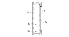
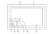
図1は本実施の形態によるアンテナ装置の構成図、図2は図1のA-A線断面図である。
本実施の形態によるアンテナ装置は、図1及び図2に示すように、金属筐体1と、ガラス2と、第1の導体3aと、第2の導体3bとを備えている。金属筐体1はアルミ等の金属で構成され、内部に図示しない液晶ディスプレイや制御基板、通信基板を収納するため箱状に構成され、正面方向に開口部1aを有する。
ガラス2は金属筐体1によって保持され、金属筐体1の開口部1aを覆うように配置された板状のガラスである。ガラス2により、金属筐体1の内部にある液晶ディスプレイ等を保護する。また、ガラス2は所定の誘電率を有する誘電体を構成している。
第1の導体3a及び第2の導体3bは、ガラス2の金属筐体1に接触する面とは反対側の面に貼付された透明導電膜である。透明導電膜(透明電極とも言う)は可視光に対して透明であり、導電性を有するシート状の媒質である。一般に透明導電膜の光透過率が高い(透明性が高い)ほどシート抵抗が高くなる。例えば、本実施の形態では、シート抵抗値が5~50Ω/sq、光透過率70~80%の透明導電膜を用いる。
実施の形態1.
図1は本実施の形態によるアンテナ装置の構成図、図2は図1のA-A線断面図である。
本実施の形態によるアンテナ装置は、図1及び図2に示すように、金属筐体1と、ガラス2と、第1の導体3aと、第2の導体3bとを備えている。金属筐体1はアルミ等の金属で構成され、内部に図示しない液晶ディスプレイや制御基板、通信基板を収納するため箱状に構成され、正面方向に開口部1aを有する。
ガラス2は金属筐体1によって保持され、金属筐体1の開口部1aを覆うように配置された板状のガラスである。ガラス2により、金属筐体1の内部にある液晶ディスプレイ等を保護する。また、ガラス2は所定の誘電率を有する誘電体を構成している。
第1の導体3a及び第2の導体3bは、ガラス2の金属筐体1に接触する面とは反対側の面に貼付された透明導電膜である。透明導電膜(透明電極とも言う)は可視光に対して透明であり、導電性を有するシート状の媒質である。一般に透明導電膜の光透過率が高い(透明性が高い)ほどシート抵抗が高くなる。例えば、本実施の形態では、シート抵抗値が5~50Ω/sq、光透過率70~80%の透明導電膜を用いる。
第2の導体3bの大部分は金属筐体1の開口部1aに配置され、その端部のみが金属筐体1の枠部に位置する(正面から見て第2の導体3bの端部が金属筐体1の枠に隠れる)よう構成されている。第1の導体3aは、ガラス2を介して金属筐体1の枠部に位置するよう配置され、第2の導体3bとの間に若干の間隙を有している。この間隙には例えば同軸ケーブル(図示せず)が高周波信号に対して電気的に接続される。すなわち、同軸ケーブルの芯線が第2の導体3bに、同軸ケーブルの外導体が第1の導体3aに接続される。これにより、第1の導体3aと第2の導体3bとの間に交流電圧が印加される。なお、第1の導体3aと第2の導体3bの間に所望の交流電圧が印加できれば、同軸ケーブル以外の伝送線路を選択しても良い。また、図1では第2の導体3bは短冊状に図示されているが、所望の周波数で共振するように設計されていれば適宜自由な形状を選択可能である。例えば図3Aのように幅が徐々に広がる形状、図3Bのように分岐を有する形状などがある。
次に、この発明の実施の形態1に係るアンテナ装置の動作について説明する。送信アンテナと受信アンテナには可逆性が成り立つため、ここでは送信アンテナとしての動作を説明する。
第1の導体3aと第2の導体3bの間に交流電圧が印加されると、両者に電荷の移動が発生して交流電流が流れる。このとき、第2の導体3bは所望の周波数で共振するように設計されたモノポールアンテナ素子となり、電波を放射する。また、第1の導体3aはガラス2を介して金属筐体1に重なるように配置されているため、第1の導体3aに交流電流が流れると、容量結合により金属筐体1にも交流電流が流れる。すなわち、金属筐体1が第2の導体3bからなるモノポールアンテナのグランドとして動作する。これにより、アンテナのグランドが十分に大きく確保でき、透明導電膜上への電流の集中を抑えることができるため、透明導電膜の導電率が低いことにより生じる損失を低減できる。
第1の導体3aと第2の導体3bの間に交流電圧が印加されると、両者に電荷の移動が発生して交流電流が流れる。このとき、第2の導体3bは所望の周波数で共振するように設計されたモノポールアンテナ素子となり、電波を放射する。また、第1の導体3aはガラス2を介して金属筐体1に重なるように配置されているため、第1の導体3aに交流電流が流れると、容量結合により金属筐体1にも交流電流が流れる。すなわち、金属筐体1が第2の導体3bからなるモノポールアンテナのグランドとして動作する。これにより、アンテナのグランドが十分に大きく確保でき、透明導電膜上への電流の集中を抑えることができるため、透明導電膜の導電率が低いことにより生じる損失を低減できる。
一般的にアンテナ上を流れる電流に対して平行に金属が近接すると、近接した金属上に逆相の電流が誘起されてアンテナの放射効率が低下する。そのため、金属筐体の内部にアンテナを設けるとアンテナの放射効率が低下する。これに対し実施の形態1のアンテナ装置では、金属筐体1の開口部1aに、モノポールアンテナ素子となる第2の導体3bを設けているため、放射効率の低下を防止できる。また、第2の導体3bは透明導電膜により構成されているため、金属筐体1の開口部1aに配置しても視認性を低下させることはない。さらに、第2の導体3bと第1の導体3aの間隙は金属筐体1で隠れる部分に位置するため、同軸ケーブル等の伝送線路が接続されてもこれによって視認性を低下させることがない。
また、第1の導体3aと金属筐体1は物理的に接触していないため、金属筐体1のグランド(フレームグランド)と第2の導体3bからなるモノポールアンテナに接続される制御基板等のグランド(シグナルグランド)を分離することができる。
また、第1の導体3aと金属筐体1は物理的に接触していないため、金属筐体1のグランド(フレームグランド)と第2の導体3bからなるモノポールアンテナに接続される制御基板等のグランド(シグナルグランド)を分離することができる。
以上説明したように、実施の形態1に係るアンテナ装置によれば、開口部を有する金属筐体と、金属筐体の開口部以外の部分に配置され、金属筐体と容量結合する第1の導体と、金属筐体の開口部に第1の導体と同一平面上に配置され、第1の導体との間に交流電圧が印加され、かつ、可視光に対して透明な第2の導体とを備えたので、視認性を低下させることなくアンテナ素子を設けることができ、さらに、フレームグランドとシグナルグランドを分離した状態で金属筐体をアンテナのグランドとして利用できるため、金属筐体に内蔵されるアンテナであっても高い放射効率のアンテナ装置を得ることができる。
また、実施の形態1のアンテナ装置によれば、第1の導体及び第2の導体のうち、少なくとも第2の導体は透明導電膜であるようにしたので、視認性を向上させたアンテナ装置を得ることができる。
実施の形態2.
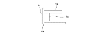
図4は実施の形態2に係るアンテナ装置を示す構成図である。図4において、金属筐体1及びガラス2は実施の形態1と同一であるため、対応する部分に同一符号を付してその説明を省略する。
実施の形態2のアンテナ装置の実施の形態1との相違点は、実施の形態1における第1の導体3aと第2の導体3bに代わって、一つの透明導電膜で形成された導体4が用いられている点である。導体4は、図4及び図5に示すように、金属筐体1の開口部1aの一つの隅部に沿う形でL字型に形成された第3の導体4aと、第3の導体4aに対して平行な第4の導体4bと、垂直な第5の導体4cからなる。実施の形態2のアンテナ装置では、第3の導体4aと第5の導体4cの間に交流電圧が印加される。このとき、開口部1aに露出している第4の導体4bの長さ(開口部1aの開口端から第4の導体4bの先端までの長さ)L、開口部1aに露出している第5の導体4cの長さ(開口部1aの開口端から第5の導体4cの基部までの長さ)H、開口部1aの開口端と第5の導体4cの間隔Dを適切に設計することで、導体4は所望の周波数で共振する逆Fアンテナとして動作する。
逆Fアンテナはモノポールアンテナを折り曲げることで得られる逆Lアンテナの電圧印加部の近くにグランドとの短絡線(ショートスタブ)を設けることでアンテナの低姿勢化や広帯域化が可能なアンテナ方式である。導体4の第3の導体4aが逆Fアンテナのグランドとなるが、第3の導体4aは金属筐体1の隅部に沿ってガラス2を介して重なるように配置され、金属筐体1と容量結合しているため、金属筐体1がアンテナグランドとして動作する。従って、実施の形態1のアンテナ装置と同様に、透明導電膜の導電率が低いことにより生じる損失を低減できる。
また、金属筐体1の開口部1aに逆Fアンテナとなる導体4を設けているため、実施の形態1で説明した動作と同様に、視認性を低下させることなく放射効率の低下を防止できる。
また、本実施の形態の逆Fアンテナでは一つの透明導電膜により一体形成しているので、短絡線を新たに設ける必要がない。このため、製作を簡略化し、低コスト化を実現することができる。
また、金属筐体1の開口部1aに逆Fアンテナとなる導体4を設けているため、実施の形態1で説明した動作と同様に、視認性を低下させることなく放射効率の低下を防止できる。
また、本実施の形態の逆Fアンテナでは一つの透明導電膜により一体形成しているので、短絡線を新たに設ける必要がない。このため、製作を簡略化し、低コスト化を実現することができる。
以上説明したように、実施の形態2のアンテナ装置によれば、開口部を有する金属筐体と、金属筐体の開口部以外の部分に開口部の隅部に沿って屈曲した形状で配置され、金属筐体と容量結合する第3の導体と、金属筐体の開口部に第3の導体と同一平面上に配置され、可視光に対して透明な第4の導体と、金属筐体の開口部に第3の導体と同一平面上に配置されると共に、第4の導体と直交して配置され、第3の導体との間に交流電圧が印加され、かつ、可視光に対して透明な第5の導体とを備え、第3の導体に対して第4の導体及び第5の導体が順番に接続されて逆Fアンテナを構成するようにしたので、開口が小さい筐体に対しても開口部にアンテナを配置することでき、小形で広帯域な特性を持つアンテナ装置を得ることができる。
また、実施の形態2のアンテナ装置によれば、逆Fアンテナのうち、少なくとも第4の導体と第5の導体は透明導電膜であるようにしたので、視認性を向上させたアンテナ装置を得ることができる。
実施の形態3.
図6は実施の形態3に係るアンテナ装置の構成図、図7は図6のB-B線断面図である。これらの図において、金属筐体1、ガラス2、第1の導体3a、第2の導体3bの構成については、実施の形態1と同様であるため、対応する部分に同一符号を付してその説明を省略する。
実施の形態3のアンテナ装置では、実施の形態1の構成に加えて給電基板5を備えている。給電基板5は、第1の導体3a及び第2の導体3bに物理的に接触し、金属筐体1に重なる部分(開口部1a以外の部分)に配置される。給電基板5は第1の導体3a及び第2の導体3bと同軸ケーブル等の伝送線路(図示せず)との間のインタフェースとして作用する。
図6は実施の形態3に係るアンテナ装置の構成図、図7は図6のB-B線断面図である。これらの図において、金属筐体1、ガラス2、第1の導体3a、第2の導体3bの構成については、実施の形態1と同様であるため、対応する部分に同一符号を付してその説明を省略する。
実施の形態3のアンテナ装置では、実施の形態1の構成に加えて給電基板5を備えている。給電基板5は、第1の導体3a及び第2の導体3bに物理的に接触し、金属筐体1に重なる部分(開口部1a以外の部分)に配置される。給電基板5は第1の導体3a及び第2の導体3bと同軸ケーブル等の伝送線路(図示せず)との間のインタフェースとして作用する。
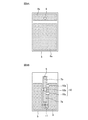
図8は給電基板5上の導体パターンの一例を示す模式的に示す説明図であり、図8Aは表面(第1の導体3a及び第2の導体3bに接触する面)、図8Bは裏面(第1の導体3a及び第2の導体3bと接触する面とは反対側の面)を表している。図8Aに示すように、給電基板5の表面側には第1の金属パターン6a及び第2の金属パターン6bが設けられている。また、図8Bに示すように、裏面側には第1の信号線7a及び第2の信号線7b、基板グランド8、スルーホール9、整合回路10、コネクタ11が設けられている。
給電基板5では、第1の金属パターン6aが第1の導体3aと物理的に接触し、第2の金属パターン6bが第2の導体3bに物理的に接触するように配置されている。また、第1の信号線7a及び第2の信号線7bと基板グランド8はコプレーナ線路を形成している。通常、コプレーナ線路の特性インピーダンスは50Ωになるよう設計される。スルーホール9は第2の金属パターン6bと第2の信号線7bとを接続するために設けられている。基板グランド8は第1の金属パターン6aと高周波的に同電位となるように多くのスルーホール(図示せず)で接続していることが望ましい。
第1の信号線7aと第2の信号線7bとは整合回路10を介して接続される。整合回路は回路素子10a,10b,10cからなり、第2の導体3bからなるモノポールアンテナのインピーダンスを第1の信号線7a及び第2の信号線7bの特性インピーダンスと整合させるために設けられる回路である。回路素子にはチップインダクタ、チップキャパシタ、ジャンパなどが用いられる。コネクタ11は、例えば表面実装タイプの同軸コネクタであり、芯線が第1の信号線7aに接続される。
金属筐体1の深さが浅かったり、ガラス2の近くに液晶ディスプレイが配置されたりすると、第2の導体3bから成るモノポールアンテナ素子に平行に金属が近づき、アンテナのインピーダンスが劣化する。これに対し、本実施の形態では整合回路10を実装した給電基板5を用いてアンテナに給電することでアンテナのインピーダンスを伝送線路の特性インピーダンスに整合させることができ、アンテナの高効率化が可能となる。
また、第2の導体3bから成るモノポールアンテナ素子と同軸ケーブル等の伝送線路が給電基板5を介して接続されるため、給電パッドなどの接続端子を透明導電膜上に形成する必要がない。これによりアンテナへの給電を簡略化することができる。さらに、図9に示すようにスペーサ12を給電基板5と金属筐体1の間に設けることで、給電基板5上の第1の金属パターン6a及び第2の金属パターン6bと第1の導体3a及び第2の導体3bの電気的接触を強固にすることも可能である。
また、第2の導体3bから成るモノポールアンテナ素子と同軸ケーブル等の伝送線路が給電基板5を介して接続されるため、給電パッドなどの接続端子を透明導電膜上に形成する必要がない。これによりアンテナへの給電を簡略化することができる。さらに、図9に示すようにスペーサ12を給電基板5と金属筐体1の間に設けることで、給電基板5上の第1の金属パターン6a及び第2の金属パターン6bと第1の導体3a及び第2の導体3bの電気的接触を強固にすることも可能である。
以上説明したように、実施の形態3のアンテナ装置によれば、第1の導体と接続される第1の金属パターンと、第2の導体に接続される第2の金属パターンとを有し、第1の金属パターン及び第2の金属パターンを介して第1の導体及び第2の導体に交流電圧を印加するための給電基板を設けたので、アンテナへの給電を簡略化することができる。
また、実施の形態3のアンテナ装置によれば、給電基板は、整合回路を介して第2の金属パターンに交流電圧を印加するようにしたので、アンテナのインピーダンスと伝送線路の特性インピーダンスを容易に整合させることができる。従って、例えば、薄型筐体等でアンテナ単独のインピーダンスを50Ωに設計できない場合でもアンテナの高効率化が可能となる。
なお、上記例では、実施の形態1の第1の導体及び第2の導体からなるモノポールアンテナに給電基板を適用した例を説明したが、実施の形態2の逆Fアンテナに対しても同様に効果を得ることができる。
すなわち、第3の導体と接続される第1の金属パターンと、第5の導体に接続される第2の金属パターンとを有し、第1の金属パターン及び第2の金属パターンを介して第3の導体及び第5の導体に交流電圧を印加するための給電基板を設けることにより、アンテナへの給電を簡略化することができる。
すなわち、第3の導体と接続される第1の金属パターンと、第5の導体に接続される第2の金属パターンとを有し、第1の金属パターン及び第2の金属パターンを介して第3の導体及び第5の導体に交流電圧を印加するための給電基板を設けることにより、アンテナへの給電を簡略化することができる。
また、実施の形態2に適用した場合でも、給電基板を、整合回路を介して第2の金属パターンに交流電圧を印加するようにすることで、アンテナのインピーダンスと伝送線路の特性インピーダンスを容易に整合させることができる。従って、例えば、薄型筐体等でアンテナ単独のインピーダンスを50Ωに設計できない場合でもアンテナの高効率化が可能となる。
なお、本願発明はその発明の範囲内において、各実施の形態の自由な組み合わせ、あるいは各実施の形態の任意の構成要素の変形、もしくは各実施の形態において任意の構成要素の省略が可能である。
また、上記実施の形態1~3では、第1の導体3a、第2の導体3b、第3の導体4a~第5の導体4cをそれぞれ透明導電膜で構成したが、可視光に対して透明な導体であればどのような素材を用いても良い。
以上のように、この発明に係るアンテナ装置は、可視光に対して透明なアンテナの構成に関するものであり、透明導電材料を用いて高い放射効率を得アンテナ装置に用いるのに適している。
1 金属筐体、1a 開口部、2 ガラス、3a 第1の導体、3b 第2の導体、4 導体、4a 第3の導体、4b 第4の導体、4c 第5の導体、5 給電基板、6a 第1の金属パターン、6b 第2の金属パターン、7a 第1の信号線、7b 第2の信号線、8 基板グランド、9 スルーホール、10 整合回路、11 コネクタ、12 スペーサ。
Claims (8)
- 開口部を有する金属筐体と、
前記金属筐体の前記開口部以外の部分に配置され、当該金属筐体と容量結合する第1の導体と、
前記金属筐体の前記開口部に前記第1の導体と同一平面上に配置され、前記第1の導体との間に交流電圧が印加され、かつ、可視光に対して透明な第2の導体とを備えたアンテナ装置。 - 前記第1の導体及び前記第2の導体のうち、少なくとも前記第2の導体は透明導電膜であることを特徴とする請求項1記載のアンテナ装置。
- 前記第1の導体と接続される第1の金属パターンと、前記第2の導体に接続される第2の金属パターンとを有し、当該第1の金属パターン及び第2の金属パターンを介して前記第1の導体及び第2の導体に交流電圧を印加するための給電基板を設けたことを特徴とする請求項1記載のアンテナ装置。
- 前記給電基板は、整合回路を介して前記第2の金属パターンに交流電圧を印加することを特徴とする請求項3記載のアンテナ装置。
- 開口部を有する金属筐体と、
前記金属筐体の前記開口部以外の部分に当該開口部の隅部に沿って屈曲した形状で配置され、前記金属筐体と容量結合する第3の導体と、
前記金属筐体の前記開口部に前記第3の導体と同一平面上に配置され、可視光に対して透明な第4の導体と、
前記金属筐体の前記開口部に前記第3の導体と同一平面上に配置されると共に、前記第4の導体と直交して配置され、前記第3の導体との間に交流電圧が印加され、かつ、可視光に対して透明な第5の導体とを備え、
前記第3の導体に対して前記第4の導体及び前記第5の導体が順番に接続されて逆Fアンテナを構成することを特徴とするアンテナ装置。 - 前記逆Fアンテナのうち、少なくとも前記第4の導体と前記第5の導体は透明導電膜であることを特徴とする請求項5記載のアンテナ装置。
- 前記第3の導体と接続される第1の金属パターンと、前記第5の導体に接続される第2の金属パターンとを有し、当該第1の金属パターン及び第2の金属パターンを介して前記第3の導体及び第5の導体に交流電圧を印加するための給電基板を設けたことを特徴とする請求項5記載のアンテナ装置。
- 前記給電基板は、整合回路を介して前記第2の金属パターンに交流電圧を印加することを特徴とする請求項7記載のアンテナ装置。
Priority Applications (5)
| Application Number | Priority Date | Filing Date | Title |
|---|---|---|---|
| CN201780092226.0A CN110770971B (zh) | 2017-06-23 | 2017-06-23 | 天线装置 |
| PCT/JP2017/023189 WO2018235260A1 (ja) | 2017-06-23 | 2017-06-23 | アンテナ装置 |
| JP2019524825A JP6602513B2 (ja) | 2017-06-23 | 2017-06-23 | アンテナ装置 |
| US16/615,007 US20200194894A1 (en) | 2017-06-23 | 2017-06-23 | Antenna device |
| EP17914905.9A EP3624261B1 (en) | 2017-06-23 | 2017-06-23 | Antenna device |
Applications Claiming Priority (1)
| Application Number | Priority Date | Filing Date | Title |
|---|---|---|---|
| PCT/JP2017/023189 WO2018235260A1 (ja) | 2017-06-23 | 2017-06-23 | アンテナ装置 |
Publications (1)
| Publication Number | Publication Date |
|---|---|
| WO2018235260A1 true WO2018235260A1 (ja) | 2018-12-27 |
Family
ID=64735997
Family Applications (1)
| Application Number | Title | Priority Date | Filing Date |
|---|---|---|---|
| PCT/JP2017/023189 Ceased WO2018235260A1 (ja) | 2017-06-23 | 2017-06-23 | アンテナ装置 |
Country Status (5)
| Country | Link |
|---|---|
| US (1) | US20200194894A1 (ja) |
| EP (1) | EP3624261B1 (ja) |
| JP (1) | JP6602513B2 (ja) |
| CN (1) | CN110770971B (ja) |
| WO (1) | WO2018235260A1 (ja) |
Families Citing this family (3)
| Publication number | Priority date | Publication date | Assignee | Title |
|---|---|---|---|---|
| US12176631B1 (en) * | 2020-08-06 | 2024-12-24 | Bae Systems Space & Mission Systems Inc. | Electrically small wideband resonant loop antenna systems and methods |
| US11943379B2 (en) * | 2020-11-26 | 2024-03-26 | Samsung Electronics Co., Ltd. | Electronic device including flexible display and control method thereof |
| US12316013B1 (en) | 2021-05-27 | 2025-05-27 | Bae Systems Space & Mission Systems Inc. | Ultra-broadband current sheet array |
Citations (6)
| Publication number | Priority date | Publication date | Assignee | Title |
|---|---|---|---|---|
| JP2009124397A (ja) * | 2007-11-14 | 2009-06-04 | Toshiba Corp | アンテナ装置及び無線装置 |
| JP2010268190A (ja) * | 2009-05-14 | 2010-11-25 | Panasonic Corp | アンテナ装置および携帯無線機 |
| WO2011111650A1 (ja) * | 2010-03-09 | 2011-09-15 | 太陽誘電株式会社 | 導体構造、透明デバイス及び電子機器 |
| US20140106684A1 (en) * | 2012-10-15 | 2014-04-17 | Qualcomm Mems Technologies, Inc. | Transparent antennas on a display device |
| US20150340756A1 (en) * | 2014-05-23 | 2015-11-26 | Nokia Corporation | Apparatus having a conductive housing and an antenna with tunable resonance |
| JP2016010042A (ja) | 2014-06-25 | 2016-01-18 | パナソニックIpマネジメント株式会社 | アンテナ装置 |
Family Cites Families (8)
| Publication number | Priority date | Publication date | Assignee | Title |
|---|---|---|---|---|
| US6384790B2 (en) * | 1998-06-15 | 2002-05-07 | Ppg Industries Ohio, Inc. | Antenna on-glass |
| US6973709B2 (en) * | 2001-04-19 | 2005-12-13 | Chunghwa Picture Tubes | Method of manufacturing printed-on-display antenna for wireless device |
| WO2007029741A1 (ja) * | 2005-09-09 | 2007-03-15 | Matsushita Electric Industrial Co., Ltd. | 無線機用アンテナ装置及び携帯無線機 |
| US20100321325A1 (en) * | 2009-06-17 | 2010-12-23 | Springer Gregory A | Touch and display panel antennas |
| KR101718016B1 (ko) * | 2010-06-04 | 2017-03-21 | 엘지전자 주식회사 | 이동 단말기 및 이동단말기 안테나의 제조방법 |
| CN105094231B (zh) * | 2015-07-28 | 2019-03-01 | 京东方科技集团股份有限公司 | 一种显示屏和便携设备 |
| US9876272B2 (en) * | 2015-08-18 | 2018-01-23 | Apple Inc. | Electronic device antenna with embedded parasitic arm |
| CN105552517A (zh) * | 2015-12-25 | 2016-05-04 | 宇龙计算机通信科技(深圳)有限公司 | 一种射频天线装置和移动终端 |
-
2017
- 2017-06-23 CN CN201780092226.0A patent/CN110770971B/zh active Active
- 2017-06-23 US US16/615,007 patent/US20200194894A1/en not_active Abandoned
- 2017-06-23 JP JP2019524825A patent/JP6602513B2/ja active Active
- 2017-06-23 EP EP17914905.9A patent/EP3624261B1/en active Active
- 2017-06-23 WO PCT/JP2017/023189 patent/WO2018235260A1/ja not_active Ceased
Patent Citations (6)
| Publication number | Priority date | Publication date | Assignee | Title |
|---|---|---|---|---|
| JP2009124397A (ja) * | 2007-11-14 | 2009-06-04 | Toshiba Corp | アンテナ装置及び無線装置 |
| JP2010268190A (ja) * | 2009-05-14 | 2010-11-25 | Panasonic Corp | アンテナ装置および携帯無線機 |
| WO2011111650A1 (ja) * | 2010-03-09 | 2011-09-15 | 太陽誘電株式会社 | 導体構造、透明デバイス及び電子機器 |
| US20140106684A1 (en) * | 2012-10-15 | 2014-04-17 | Qualcomm Mems Technologies, Inc. | Transparent antennas on a display device |
| US20150340756A1 (en) * | 2014-05-23 | 2015-11-26 | Nokia Corporation | Apparatus having a conductive housing and an antenna with tunable resonance |
| JP2016010042A (ja) | 2014-06-25 | 2016-01-18 | パナソニックIpマネジメント株式会社 | アンテナ装置 |
Non-Patent Citations (1)
| Title |
|---|
| See also references of EP3624261A4 |
Also Published As
| Publication number | Publication date |
|---|---|
| CN110770971A (zh) | 2020-02-07 |
| JP6602513B2 (ja) | 2019-11-06 |
| EP3624261A1 (en) | 2020-03-18 |
| EP3624261A4 (en) | 2020-05-13 |
| JPWO2018235260A1 (ja) | 2019-11-07 |
| US20200194894A1 (en) | 2020-06-18 |
| EP3624261B1 (en) | 2021-08-25 |
| CN110770971B (zh) | 2021-08-13 |
Similar Documents
| Publication | Publication Date | Title |
|---|---|---|
| TWI520437B (zh) | 具有基於槽孔之寄生元件之天線結構 | |
| JP5414451B2 (ja) | アンテナ装置 | |
| US8982003B2 (en) | Slot antenna, electronic apparatus, and method for manufacturing slot antenna | |
| JP5482171B2 (ja) | アンテナ装置、及び無線端末装置 | |
| US9746571B2 (en) | Proximity sensor antenna device and antenna structure thereof | |
| JP6932724B2 (ja) | アンテナ用コネクタ、このコネクタを備えたグレージング、およびこのコネクタを備えたアンテナシステム | |
| CN110941113A (zh) | 显示装置及其制作方法 | |
| CN110692169A (zh) | 便携式电子设备 | |
| JP5029559B2 (ja) | アンテナ及びそれを備えた電気機器 | |
| JP6602513B2 (ja) | アンテナ装置 | |
| TWI513102B (zh) | 通訊裝置 | |
| JPWO2007083500A1 (ja) | アンテナ付き画像表示装置 | |
| JP2010028494A (ja) | アンテナ及びそれを備えた電気機器 | |
| US10181638B2 (en) | Radiofrequency antenna device | |
| CN103703618B (zh) | 天线装置以及天线的安装方法 | |
| CN108767443A (zh) | 一种天线装置及电子设备 | |
| TWI736285B (zh) | 天線結構 | |
| JP4775301B2 (ja) | 透明アンテナ | |
| CN107871931B (zh) | 天线结构及具有该天线结构的无线通信装置 | |
| TWI613865B (zh) | 電子裝置 | |
| CN101483269B (zh) | 应用于无线广域网的天线 | |
| TWI532255B (zh) | Transmission line load antenna module | |
| JP2007129597A (ja) | 多周波アンテナ | |
| JP2008187447A (ja) | アンテナおよびアンテナの部品 | |
| CN119833930A (zh) | 电子设备 |
Legal Events
| Date | Code | Title | Description |
|---|---|---|---|
| 121 | Ep: the epo has been informed by wipo that ep was designated in this application |
Ref document number: 17914905 Country of ref document: EP Kind code of ref document: A1 |
|
| ENP | Entry into the national phase |
Ref document number: 2019524825 Country of ref document: JP Kind code of ref document: A |
|
| ENP | Entry into the national phase |
Ref document number: 2017914905 Country of ref document: EP Effective date: 20191211 |
|
| NENP | Non-entry into the national phase |
Ref country code: DE |