WO2019003290A1 - 電力変換装置 - Google Patents
電力変換装置 Download PDFInfo
- Publication number
- WO2019003290A1 WO2019003290A1 PCT/JP2017/023496 JP2017023496W WO2019003290A1 WO 2019003290 A1 WO2019003290 A1 WO 2019003290A1 JP 2017023496 W JP2017023496 W JP 2017023496W WO 2019003290 A1 WO2019003290 A1 WO 2019003290A1
- Authority
- WO
- WIPO (PCT)
- Prior art keywords
- arm
- input
- semiconductor switching
- circuit
- switching elements
- Prior art date
- Legal status (The legal status is an assumption and is not a legal conclusion. Google has not performed a legal analysis and makes no representation as to the accuracy of the status listed.)
- Ceased
Links
Images


Classifications
-
- H—ELECTRICITY
- H02—GENERATION; CONVERSION OR DISTRIBUTION OF ELECTRIC POWER
- H02M—APPARATUS FOR CONVERSION BETWEEN AC AND AC, BETWEEN AC AND DC, OR BETWEEN DC AND DC, AND FOR USE WITH MAINS OR SIMILAR POWER SUPPLY SYSTEMS; CONVERSION OF DC OR AC INPUT POWER INTO SURGE OUTPUT POWER; CONTROL OR REGULATION THEREOF
- H02M1/00—Details of apparatus for conversion
- H02M1/32—Means for protecting converters other than automatic disconnection
-
- H—ELECTRICITY
- H02—GENERATION; CONVERSION OR DISTRIBUTION OF ELECTRIC POWER
- H02M—APPARATUS FOR CONVERSION BETWEEN AC AND AC, BETWEEN AC AND DC, OR BETWEEN DC AND DC, AND FOR USE WITH MAINS OR SIMILAR POWER SUPPLY SYSTEMS; CONVERSION OF DC OR AC INPUT POWER INTO SURGE OUTPUT POWER; CONTROL OR REGULATION THEREOF
- H02M1/00—Details of apparatus for conversion
- H02M1/42—Circuits or arrangements for compensating for or adjusting power factor in converters or inverters
- H02M1/4208—Arrangements for improving power factor of AC input
-
- H—ELECTRICITY
- H02—GENERATION; CONVERSION OR DISTRIBUTION OF ELECTRIC POWER
- H02M—APPARATUS FOR CONVERSION BETWEEN AC AND AC, BETWEEN AC AND DC, OR BETWEEN DC AND DC, AND FOR USE WITH MAINS OR SIMILAR POWER SUPPLY SYSTEMS; CONVERSION OF DC OR AC INPUT POWER INTO SURGE OUTPUT POWER; CONTROL OR REGULATION THEREOF
- H02M7/00—Conversion of AC power input into DC power output; Conversion of DC power input into AC power output
- H02M7/42—Conversion of DC power input into AC power output without possibility of reversal
- H02M7/44—Conversion of DC power input into AC power output without possibility of reversal by static converters
- H02M7/48—Conversion of DC power input into AC power output without possibility of reversal by static converters using discharge tubes with control electrode or semiconductor devices with control electrode
- H02M7/483—Converters with outputs that each can have more than two voltages levels
- H02M7/4835—Converters with outputs that each can have more than two voltages levels comprising two or more cells, each including a switchable capacitor, the capacitors having a nominal charge voltage which corresponds to a given fraction of the input voltage, and the capacitors being selectively connected in series to determine the instantaneous output voltage
-
- H—ELECTRICITY
- H02—GENERATION; CONVERSION OR DISTRIBUTION OF ELECTRIC POWER
- H02M—APPARATUS FOR CONVERSION BETWEEN AC AND AC, BETWEEN AC AND DC, OR BETWEEN DC AND DC, AND FOR USE WITH MAINS OR SIMILAR POWER SUPPLY SYSTEMS; CONVERSION OF DC OR AC INPUT POWER INTO SURGE OUTPUT POWER; CONTROL OR REGULATION THEREOF
- H02M7/00—Conversion of AC power input into DC power output; Conversion of DC power input into AC power output
- H02M7/42—Conversion of DC power input into AC power output without possibility of reversal
- H02M7/44—Conversion of DC power input into AC power output without possibility of reversal by static converters
- H02M7/48—Conversion of DC power input into AC power output without possibility of reversal by static converters using discharge tubes with control electrode or semiconductor devices with control electrode
- H02M7/53—Conversion of DC power input into AC power output without possibility of reversal by static converters using discharge tubes with control electrode or semiconductor devices with control electrode using devices of a triode or transistor type requiring continuous application of a control signal
- H02M7/537—Conversion of DC power input into AC power output without possibility of reversal by static converters using discharge tubes with control electrode or semiconductor devices with control electrode using devices of a triode or transistor type requiring continuous application of a control signal using semiconductor devices only, e.g. single switched pulse inverters
- H02M7/5387—Conversion of DC power input into AC power output without possibility of reversal by static converters using discharge tubes with control electrode or semiconductor devices with control electrode using devices of a triode or transistor type requiring continuous application of a control signal using semiconductor devices only, e.g. single switched pulse inverters in a bridge configuration
- H02M7/53871—Conversion of DC power input into AC power output without possibility of reversal by static converters using discharge tubes with control electrode or semiconductor devices with control electrode using devices of a triode or transistor type requiring continuous application of a control signal using semiconductor devices only, e.g. single switched pulse inverters in a bridge configuration with automatic control of output voltage or current
Definitions
- the present disclosure relates to a self-excited power converter configured by connecting a plurality of converter cells in a cascade, and is suitably used, for example, for high voltage DC power transmission, frequency converter, reactive power compensation device, etc. is there.
- a modular multilevel converter is known as a large-capacity power converter connected to a power system.
- the modular multi-level converter has an upper arm circuit connected to the high potential side DC terminal and a lower arm circuit connected to the low potential side DC terminal in each phase of alternating current.
- Each arm circuit is configured by connecting a large number of converter cells in a cascade.
- the converter cells are also referred to as submodules.
- the converter cell comprises a capacitor as an energy storage, first and second input / output nodes, and a bridge circuit for switching between connection / disconnection between these input / output nodes and the capacitor.
- a bridge circuit a half bridge type or a full bridge type is used.
- a bypass switch is provided in parallel with each converter cell (see, for example, paragraph 0003 of WO 2014/148100 (Patent Document 1)). If a converter cell fails, the output of the converter cell is shorted by turning on the parallel connected bypass switch. By this, operation of MMC can be continued.
- the inventors of the present application are promoting development of an MMC having an increased current capacity by providing two or more semiconductor switching elements in parallel in each arm of a bridge circuit constituting a converter cell. Further, in the MMC of such a configuration, if a bypass switch as described in the above-mentioned document is provided, the volume of the converter cell is increased and the cost is increased.
- the present disclosure takes the above problems into consideration, and an object thereof is to provide a power converter capable of suppressing the volume and cost of a cell converter.
- the power converter of one embodiment comprises a plurality of converter cells cascaded together.
- Each converter cell includes a first input / output node, a second input / output node, an energy storage, a bridge circuit, and a drive control unit.
- a bridge circuit is provided to switch the connection and disconnection between the first and second input / output nodes and the energy storage.
- a plurality of semiconductor switching elements are provided in parallel to each of the arms provided with the semiconductor switching elements among the plurality of arms constituting the bridge circuit.
- the drive control unit is configured to control the bridge circuit in accordance with an externally provided command when none of the plurality of predetermined abnormal modes is detected. When the drive control unit detects at least one of the plurality of abnormal modes, the drive control unit turns on all the semiconductor switching elements provided in at least one of the plurality of arms constituting the bridge circuit. It is configured to short between the first and second input / output nodes.
- a semiconductor switching element forming a bridge circuit in place of the conventional bypass switch, a semiconductor switching element forming a bridge circuit can be used, so that the volume and cost of the cell converter can be suppressed.
- a semiconductor switching element forming a bridge circuit since a plurality of semiconductor switching elements are provided in parallel in each arm of the bridge circuit, the possibility that the plurality of semiconductor switching elements will simultaneously have an open failure is low.
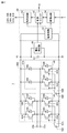
- FIG. 1 is a diagram showing a schematic configuration example of a power conversion device of a first embodiment. It is a figure which shows the modification of the connection part of AC circuit and each leg circuit. It is a figure which shows the other modification of the connection part of an alternating current circuit and each leg circuit. It is a figure which shows the example of a rough structure of the HVDC system using the power converter device of FIG. It is a figure which shows the example of a rough structure of the BTB system using the power converter device of FIG. It is a figure which shows an example of the converter cell which comprises each leg circuit of FIG. 5 is a flow chart illustrating the operation of the converter cell. 5 is a flow chart showing the operation of the central control unit in connection with the detection of an abnormal mode.
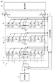
- FIG. 1 is a diagram showing a schematic configuration example of the power conversion device of the first embodiment.
- power conversion device 1 includes main circuits: leg circuits 4 u, 4 v, 4 w (in the case of showing an unspecified one, described as leg circuit 4), and central control unit 3.
- leg circuits 4 u, 4 v, 4 w in the case of showing an unspecified one, described as leg circuit 4
- central control unit 3 In the present embodiment, the entire leg circuits 4 u, 4 v, 4 w will be referred to as the power conversion circuit unit 2.
- the leg circuit 4 is provided in each of a plurality of phases forming alternating current, and is connected between the alternating current circuit 12 and the direct current circuit 14 to perform power conversion between the two circuits.
- FIG. 1 shows the case where the AC circuit 12 is a three-phase AC, and three leg circuits 4u, 4v, 4w are provided corresponding to the u phase, the v phase, and the w phase, respectively.
- AC terminals Nu, Nv, Nw provided in the leg circuits 4 u, 4 v, 4 w, respectively, are connected to the AC circuit 12 via the interconnection transformer 13.
- AC circuit 12 is, for example, an AC power system including an AC power supply and the like. In FIG. 1, the connection between the AC terminals Nv and Nw and the interconnection transformer 13 is not shown for ease of illustration.
- the DC terminals Np and Nn (that is, the high potential side DC terminal Np and the low potential side DC terminal Nn) provided in common to the respective leg circuits 4 are connected to the DC circuit 14.
- the DC circuit 14 corresponds to a DC power system in a high voltage direct current (HVDC) system of FIG. 4 described later, or a connection terminal to another power conversion device in a BTB (back to back) system of FIG. Do.
- HVDC high voltage direct current
- the interconnection transformer 13 of FIG. 1 may be connected to the AC circuit 12 via an interconnection reactor. Further, as shown in FIG. 2 and FIG. 3, the AC circuit 12 and each leg circuit 4 may be connected in an AC manner. The detailed configuration of the connection portion between the AC circuit 12 and each leg circuit 4 in this case will be described later.
- the leg circuit 4 u is divided into an upper arm circuit 5 from the high potential side direct current terminal Np to the alternating current terminal Nu and a lower arm circuit 6 from the low potential side direct current terminal Nn to the alternating current terminal Nu.
- a connection point between the upper arm circuit 5 and the lower arm circuit 6 (that is, the AC terminal Nu) is connected to the transformer 13. Further, the high potential side DC terminal Np and the low potential side DC terminal Nn are connected to the DC circuit 14. Since the leg circuits 4v and 4w also have the same configuration, the leg circuit 4u will be described as a representative.
- Upper arm circuit 5 includes a plurality of cascade-connected converter cells 7 and a reactor 8p.
- the plurality of converter cells 7 and the reactor 8p are connected in series with each other.
- the converter cell 7 may hereinafter be referred to as the cell 7 for the sake of simplicity.
- lower arm circuit 6 includes a plurality of cells 7 connected in cascade and reactor 8 n.
- the plurality of cells 7 and the reactor 8 n are connected in series with one another.
- the arm currents Ipu and Ipn change rapidly at the moment when the cell in the leg circuit turns on or off and the output voltage suddenly changes, or in the event of an accident such as the AC circuit 12 or the DC circuit 14. It is provided not to.
- the position where reactor 8p is inserted may be any position of upper arm circuit 5 of leg circuit 4u, and the position where reactor 8n is inserted is any position of lower arm circuit 6 of leg circuit 4u. May be There may be a plurality of reactors 8p and 8n respectively. The inductance values of the reactors may be different from each other. Furthermore, only the reactor 8 p of the upper arm circuit 5 or only the reactor 8 n of the lower arm circuit 6 may be provided.
- the power conversion device 1 of FIG. 1 further includes an AC voltage detector 10, an AC current detector 16, and a DC voltage detector 11p as a detector for measuring an electric quantity (current, voltage, etc.) used for control. , 11 n and arm current detectors 9 p and 9 n provided in each leg circuit 4.
- the AC voltage detector 10 detects the voltage value of each of the U phase, the V phase, and the W phase of the AC circuit 12.
- the alternating current detector 16 detects current values Iacu, Iacv, and Iacw of the U-phase, V-phase, and W-phase of the AC circuit 12.
- the DC voltage detector 11 p detects the voltage of the high potential side DC terminal Np connected to the DC circuit 14.
- the direct current voltage detector 11 n detects the voltage of the low potential side direct current terminal Nn connected to the direct current circuit 14.
- the arm current detectors 9p and 9n provided in the U-phase leg circuit 4u respectively detect an arm current Ipu flowing in the upper arm circuit 5 and an arm current Inu flowing in the lower arm circuit 6.
- arm current detectors 9p and 9n provided in the V phase leg circuit 4v respectively detect an upper arm current Ipv and a lower arm current Inv.
- the arm current detectors 9p and 9n provided in the W phase leg circuit 4w respectively detect the upper arm current Ipw and the lower arm current Inw. Based on these arm currents, it is possible to calculate the DC current Idc flowing through the DC circuit 14 and the circulating current circulating between the respective leg circuits.
- the signal detected by the above detector is input to the central control unit 3.
- Central control unit 3 further receives a signal representing a detected value of the cell capacitor voltage from each cell 7.
- the central control unit 3 controls / controls the operation state of each cell 7 based on the detection signal of each detector and the information of the cell capacitor voltage and the operation / stop for protecting each cell 7
- a command (operation command or stop command) is output to each cell 7.
- signal lines of signals input from each detector to central control device 3 and signal lines of signals transmitted between central control device 3 and each cell 7 are Although partially described collectively, in practice each detector and each cell 7 are individually provided. The signal lines between each cell 7 and the central control device 3 may be provided separately for transmission and reception. Further, in the case of the present embodiment, these signal lines are formed of optical fibers from the viewpoint of noise resistance.
- each arm circuit 5, 6 may be provided with a plurality of bypass circuits.
- the plurality of converter cells 7 constituting each arm circuit are divided into a plurality of blocks, and a bypass circuit is provided for each block.
- the bypass circuit is for protecting the power conversion circuit unit 2 by supplying a fault current when the DC circuit is broken. For example, the direction from the low potential side DC terminal Nn to the high potential side DC terminal Np is forward. To be connected by series connected diodes.
- bypass circuit is different from the bypass switch described in the background art.
- bypass switches are provided for shorting the output terminals of the converter cell 7 in the event of a failure of the converter cell 7 itself.
- the power converter 1 of the present embodiment is characterized in that a bypass switch is not connected between the input and output terminals of each converter cell 7.
- FIG. 1 shows an example in which the AC circuit 12 and the power conversion circuit unit 2 are connected in a direct current manner via the AC terminals Nu, Nv and Nw respectively provided in the leg circuits 4u, 4v and 4w.
- AC circuit 12 and each leg circuit 4 may be AC-connected via a transformer.
- FIG. 2 is a view showing a modification of the connection portion between the AC circuit and each leg circuit.
- AC circuit 12 and leg circuits 4u, 4v, 4w are connected via three-phase transformer 80B.
- primary windings 81u, 81v, and 81w are ⁇ -connected. Specifically, the primary winding 81 u of the three-phase transformer 80 B is connected between the U phase and the V phase of the AC circuit 12. The primary winding 81 v of the three-phase transformer 80 B is connected between the V phase and the W phase of the AC circuit 12. The primary winding 81 w of the three-phase transformer 80 B is connected between the W phase and the U phase of the AC circuit 12.
- the secondary windings 82u, 82v, 82w of the three-phase transformer 80B are magnetically coupled to the primary windings 81u, 81v, 81w, respectively, via a common iron core. Further, secondary winding 82u is connected in series with U-phase arm circuits 5u and 6u, secondary winding 82v is connected in series with V-phase arm circuits 5v and 6v, and secondary winding 82w is W-phase Are connected in series with the arm circuits 5w and 6w.
- each of secondary windings 82u, 82v, 82w doubles as reactors 8p, 8n of each phase.
- the secondary windings 82u, 82v, 82w of the three-phase transformer 80B may be provided separately from the reactors 8p, 8n.
- the direct current magnetic flux generated in the iron core can be canceled by flowing a direct current component to the ⁇ -connected primary windings 81u, 81v, 81w.
- FIG. 3 is a view showing another modified example of the connection portion between the AC circuit and each leg circuit.
- AC circuit 12 and leg circuits 4u, 4v, 4w are connected via three-winding three-phase transformer 80C.
- each of primary windings 81u, 81v and 81w of three-phase transformer 80C in FIG. 3 is connected to each of the U-phase, V-phase and W-phase transmission lines of AC circuit 12 via interconnection transformer 13 Each connected.
- the other ends of primary windings 81u, 81v, 81w of three-phase transformer 80C are connected to a common neutral point 84. That is, in the case of FIG. 3, the primary windings 81u, 81v, 81w are Y-connected.
- the secondary windings 82u, 82v, 82w of the three-phase transformer 80C are magnetically coupled to the primary windings 81u, 81v, 81w via common iron cores, respectively.
- the three-phase transformer 80C of FIG. 3 is further provided with tertiary windings 83u, 83v, 83w connected in series with the secondary windings 82u, 82v, 82w, respectively.
- the secondary windings of each phase and the corresponding tertiary windings are connected in reverse polarity and wound around a common iron core. Further, the connection point between the secondary winding of each phase and the corresponding tertiary winding is connected to a common neutral point 85.
- secondary winding 82u and tertiary winding 83u are connected in series with U-phase arm circuits 5u and 6u.
- Secondary winding 82v and tertiary winding 83v are connected in series with V-phase arm circuits 5v and 6v.
- the secondary winding 82w and the tertiary winding 83w are connected in series with the W-phase arm circuits 5w and 6w.
- each of the secondary windings 82u, 82v, 82w and each of the tertiary windings 83u, 83v, 83w double as the reactors 8p, 8n of each phase.
- the secondary windings 82u, 82v, 82w and the tertiary windings 83u, 83v, 83w of the three-phase transformer 80C may be provided separately from the reactors 8p, 8n.
- the DC electromotive force generated in the secondary winding by the arm current of each phase (U phase: Ipu, Inu, V phase: Ipv, Inv, W phase: Ipw, Inw) Since the electromotive forces generated in the tertiary winding mutually cancel each other, there is an advantage that no DC magnetic flux is generated in the iron core.
- FIG. 4 is a view showing a schematic configuration example of an HVDC system using the power conversion device of FIG.
- the HVDC (High Voltage Direct Current) system converts high voltage AC power into DC power and then performs DC long distance power transmission.
- the power conversion device 1 described in FIG. 1 is used for AC / DC conversion.
- the high potential side DC terminal Np of the power conversion device 1 is connected to the high potential side transmission line 20p
- the low potential side DC terminal Nn of the power conversion device 1 is connected to the low potential side transmission line 20n.
- a DC power system including transmission lines 20p and 20n corresponds to the DC circuit 14 of FIG.
- the configuration of the HVDC system of FIG. 4 is an example, and is not limited to this example.
- the connection between AC circuit 12 and each leg circuit 4 may be three-phase transformers 80B and 80C as described in FIGS. 2 and 3.
- FIG. 5 is a diagram showing a schematic configuration example of a BTB system using the power conversion device of FIG.
- the BTB (Back to Back) system performs power interchange between two AC circuits by performing forward conversion that converts alternating current to direct current and reverse conversion that converts direct current to alternating current.
- the power conversion device 1 described in FIG. 1 is used for forward conversion and reverse conversion.
- BTB system 70 controls power conversion circuit units 2A and 2B sharing power supply circuit terminals 2A and 2B sharing high potential side DC terminal Np and low potential side DC terminal Nn with each other, and power conversion circuit units 2A and 2B. And a central control unit 3.
- the AC terminals Nu, Nv, Nw of the power conversion circuit unit 2A are connected to an AC circuit 12A (AC power system) via an interconnection transformer 13A.
- AC terminals Nu, Nv and Nw of the power conversion circuit unit 2B are connected to an AC circuit 12B (AC power system) via an interconnection transformer 13B.
- the high potential side direct current terminal Np and the low potential side direct current terminal Nn shared by the power conversion circuit units 2A and 2B correspond to the direct current circuit 14 of the power conversion device 1.
- the configuration of the BTB system 70 of FIG. 5 is an example, and is not limited to this example.
- the connection portion between the AC circuit 12A and each leg circuit of the power conversion circuit unit 2A and the connection portion between the AC circuit 12B and each leg circuit of the power conversion circuit unit 2B are the same as described with reference to FIGS. It may be phase transformers 80B and 80C.
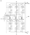
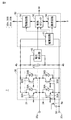
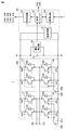
- FIG. 6 is a view showing an example of a converter cell which constitutes each of the leg circuits of FIG.
- the converter cell 7 shown in FIG. 6 includes a first input / output node 25p, a second input / output node 25n, a half bridge type bridge circuit 30, a DC capacitor 47 as an energy storage, and a drive control unit. 50, a voltage detector 48, a latch switch 58, and a battery 59.
- the battery 59 is also referred to as a battery power supply unit.
- the input / output node 25p is connected to the input / output node 25n of the adjacent converter cell 7 on the side close to the high potential side DC terminal Np.
- the input / output node 25p of the converter cell 7 disposed close to the highest potential side DC terminal Np is connected to the high potential side DC terminal Np.
- the input / output node 25n is connected to the input / output node 25p of the adjacent converter cell 7 on the side close to the low potential side DC terminal Nn.
- the input / output node 25n of the converter cell 7 disposed close to the lowest potential side DC terminal Nn is connected to the low potential side DC terminal Nn.
- the half bridge type bridge circuit 30 includes a first arm 31 connected between a node 45 on the positive electrode side of the DC capacitor 47 and an input / output node 25p, a node 46 on the negative electrode side of the DC capacitor 47, and an input / output node 25p. And a second arm 34 connected therebetween.
- the input / output node 25 n is directly connected to the node 46.
- the first arm 31 includes semiconductor switching elements 32A and 32B (hereinafter may be simply referred to as switching elements) and diodes 33A and 33B connected in parallel to each other.
- the diodes 33A and 33B are connected in anti-parallel (that is, in parallel and in the reverse bias direction) with the switching elements 32A and 32B, respectively.
- the second arm 34 includes semiconductor switching elements 35A, 35B and diodes 36A, 36B connected in parallel to each other.
- the diodes 36A and 36B are connected in anti-parallel to the switching elements 35A and 35B, respectively.
- FIG. 6 shows a case where two semiconductor switching elements are provided in parallel in each arm of bridge circuit 30, even if two or more semiconductor switching elements are provided in parallel in each arm. Good.
- semiconductor switching elements 32A, 32B, 35A, 35B for example, self-excited semiconductor switching elements such as IGBTs (Insulated Gate Bipolar Transistors) or GCTs (Gate Commutated Turn-off thyristors) are used.
- IGBTs Insulated Gate Bipolar Transistors
- GCTs Gate Commutated Turn-off thyristors
- the voltage detector 48 detects the DC voltage held by the DC capacitor 47.
- the direct current capacitor 47 is, for example, a direct current voltage transformer (DCVT).
- DCVT direct current voltage transformer
- the voltage of the DC capacitor 47 is also referred to as a cell capacitor voltage.
- the drive control unit 50 includes a power supply circuit 51, a control logic 52, a drive circuit 53, and a communication circuit 54. Each of these elements may be formed on a separate circuit board, or at least a part of the elements may be formed on a common circuit board.
- the control logic 52 may be configured as a dedicated circuit, or may be configured using an FPGA (Field Programmable Gate Array). Alternatively, the function of the control logic 52 may be realized by a microcomputer provided with a CPU (Central Processing Unit), a memory, and the like.
- the power supply circuit 51 generates drive voltages of various magnitudes used in the control logic 52, the drive circuit 53, the communication circuit 54 and the like in the converter cell 7 based on the voltage stored in the DC capacitor 47. . Therefore, the power supply circuit 51 operates only when electric charge is accumulated in the DC capacitor 47 at the time of startup of the power conversion device 1, whereby the other circuits constituting the drive control unit 50 operate.
- the communication circuit 54 communicates with a communication circuit provided in the central control unit 3. An optical fiber is used for this communication from the viewpoint of noise resistance.
- the drive circuit 53 generates gate drive signals for the semiconductor switching elements 32A, 32B, 35A, 35B based on the on / off command from the control logic 52.
- the control logic 52 controls on / off of the semiconductor switching elements 32A, 32B, 35A, 35B based on the control command and the operation / stop command received from the central control device 3 via the communication circuit 54.
- the on / off signal from the control logic 52 is amplified by the drive circuit 53 to generate a gate drive signal.
- the control logic 52 further sends information on the voltage of the DC capacitor 47 detected by the voltage detector 48 to the central control unit 3.
- control logic 52 is configured to detect a plurality of abnormal modes in the converter cell 7 using a plurality of sensors (not shown). For example, the following anomaly detection is performed.
- the abnormal mode is not limited to the following.
- control logic 52 When the control logic 52 detects at least one of a plurality of predetermined abnormal modes, all the semiconductor switching elements 35A and 35B constituting the second arm 34 are turned on (that is, closed). Control to short-circuit between the input and output nodes 25p, 25n. Specifically, the control logic 52 applies the output voltage of the battery 59 to the gates of the semiconductor switching elements 35A and 35B by turning on (i.e., closing) the switch 58.
- the switch 58 is preferably a latch type switch that maintains the on state even when the drive signal from the control logic 52 is not supplied. Thus, even if the power supply circuit 51 does not operate due to the voltage of the DC capacitor 47 being discharged after the short circuit between the input and output nodes 25p, 25n, the semiconductor switching devices 35A, 35B can be maintained in the on state.
- the converter cell 7 of FIG. 6 is characterized in that the bypass switch conventionally required for shorting between the input and output nodes 25p and 25n is not provided.
- the bypass switch conventionally required for shorting between the input and output nodes 25p and 25n is not provided.
- the semiconductor switching elements 35A and 35B constituting the second arm 34 By turning on the semiconductor switching elements 35A and 35B constituting the second arm 34, the same effect as that of the conventional bypass switch being turned on can be achieved.
- the semiconductor switching elements 35A and 35B can be used instead of the bypass switch.
- the power consumption of the semiconductor switching elements 35A and 35B is mainly the conduction loss and the switching loss, and when the semiconductor switching elements 35A and 35B are always in the on state, there is no switching loss, so the power consumption does not become a problem.
- each of the arm circuits 5 and 6 constituting the power conversion device 1 one or more redundant converter cells 7 are provided. As a result, even if the input and output nodes 25p and 25n of the converter cell 7 in the abnormal mode are short-circuited, no problem occurs in the operation of the power conversion device 1.
- control logic 52 causes the semiconductor switching elements 32A, 32B, and so that one of the first arm 31 and the second arm 34 becomes conductive and the other becomes nonconductive in accordance with the control command received from the central control device 3.
- Control 35A and 35B are a voltage command value for each arm, and each converter cell 7 controls the semiconductor switching elements 32A, 32B, 35A, 35B to output a zero voltage or a cell capacitor voltage according to the voltage command value.
- the converter cell 7 shown in FIG. 6 turns on the switching elements 32A, 32B constituting the first arm 31 and the switching elements 35A, 35B constituting the second arm 34 in an ON state alternately to achieve zero voltage.
- a positive voltage depending on the voltage of the DC capacitor 47 can be output.
- the central control unit 3 of FIG. 1 outputs a stop command to each converter cell 7 when detecting an overcurrent of the arm current.
- the control logic 52 turns off all the semiconductor switching elements 32A, 32B, 35A, 35B constituting the first arm 31 and the second arm 34 for circuit protection.
- the control logic 52 applies the output voltage of the battery 59 to the semiconductor switching elements 35A and 35B by turning on (i.e., closing) the switch 58.
- the semiconductor switching elements 35A and 35B constituting the second arm 34 are all turned on, thereby shorting between the input and output nodes 25p and 25n.
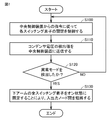
- FIG. 7 is a flow chart showing the operation of the converter cell. The above description will be summarized below with reference to FIGS. 6 and 7.
- control logic 52 If the control logic 52 has not detected any of the plurality of abnormal modes of the converter cell 7 (NO in step S120), the control logic 52 follows the control command and the operation / stop command from the central control device 3 in step S100.
- the semiconductor switching elements 32A, 32B, 35A, 35B are controlled. Furthermore, in this case, the control logic 52 transmits information on the voltage detection value of the DC capacitor 47 to the central control device 3 in step S110.
- control logic 52 detects at least one of the plurality of abnormal modes of the converter cell 7 (NO in step S120)
- the control logic 52 is provided in the lower arm 34 configuring the bridge circuit 30 in step S130.
- the first and second input / output nodes 25p and 25n are short-circuited by turning on all the switching elements. This allows MMC operation to continue using converter cells other than the failed cell.
- the bridge circuit may differ depending on the configuration of the bridge circuit, in which arm all switching elements are turned on in order to short-circuit between the first and second input / output nodes 25p and 25n There must be.
- all switching elements of the lower second arm 34 and the fourth arm 40 may be turned on, or the upper first arm 31 and the third arm All 37 switching elements may be turned on. Therefore, more generally, when the control logic 52 detects at least one of the plurality of abnormal modes of the converter cell 7 (NO in step S120), the control logic 52 selects one of the plurality of arms constituting the bridge circuit. All switching elements of at least one arm, which are necessary to short between the first and second input / output nodes 25p and 25n, are turned on.
- each arm circuit 5, 6 constituting the power conversion device 1 is provided with a predetermined number of redundant converter cells 7.
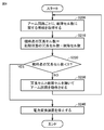
- FIG. 8 is a flow chart showing the operation of the central control unit in connection with the detection of the abnormal mode.
- central control device 3 detects the number of failed cells for each arm circuit (ie, short circuit between input / output nodes 25p and 25n due to detection of abnormal mode). Get information about the number of cells in a state.
- the central control unit 3 calculates the current number of redundant cells by subtracting the number of failed cells from the number of redundant cells in the initial state. Then, when the current number of redundant cells is smaller than 0, that is, when the number of faulty cells exceeds the initial value of the number of redundant cells (YES in step S220), central control device 3 converts the power converter in step S240. Stop the operation of 1. Specifically, both the AC circuit breaker (not shown) between AC circuit 12 and the DC circuit breaker (not shown) between DC circuit 14 are opened and power conversion circuit unit 2 The respective converter cells 7 are controlled so that all of the semiconductor switching elements 32A, 32B, 35A, 35B provided in the respective converter cells 7 constituting the switch are turned off.
- step S230 central control device 3 selects each arm circuit 5 by converter cells 7 excluding the redundant cells and the defective cells at the present time. , 6 operate. In this case, the central control device 3 may output a control command such that the switching elements 35A and 35B constituting the second arm 34 are always in the on state with respect to the redundant cell at the current time.
- central control device 3 sets a voltage command value corresponding to the number of effective cells excluding the current number of redundant cells and the number of faulty cells (the number of effective cells is constant regardless of the number of faulty cells) as a control command. It may be made to output to each arm circuit 5,6. Based on this voltage command value, the control logic 52 of the converter cell 7 corresponding to the redundant cell always turns on the switching elements 35A and 35B that constitute the second arm 34.
- each converter cell 7 is configured by the half bridge type bridge circuit 30.
- each converter cell 7 is comprised by the bridge circuit of a full bridge type
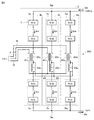
- FIG. 9 is a diagram showing another configuration example of the converter cell that constitutes each leg circuit of FIG.
- the converter cell 7 of FIG. 9 differs from the converter cell 7 of FIG. 6 in that a full bridge type bridge circuit 30A is provided instead of the half bridge type bridge circuit 30.
- a full bridge type bridge circuit 30A is provided instead of the half bridge type bridge circuit 30.
- the converter cell 7 of FIG. 9 includes a first input / output node 25p, a second input / output node 25n, a full bridge type bridge circuit 30A, a DC capacitor 47 as an energy storage, and a drive control unit 50. , A voltage detector 48, latch switches 58A and 58B, and batteries 59A and 59B.
- the batteries 59A and 59B are collectively referred to as a battery power supply unit.
- the battery power supply unit may be configured by the two batteries 59A and 59B as described above, or may be configured by a single battery.
- the full bridge type bridge circuit 30A includes a first arm 31 connected between the node 45 on the positive electrode side and the input / output node 25p, and a third arm connected between the node 46 on the negative electrode side and the input / output node 25p.
- the configurations of the first arm 31 and the second arm 34 are the same as in the case of FIG.
- the third arm 37 includes semiconductor switching elements 38A and 38B connected in parallel to one another and diodes 39A and 39B.
- the diodes 39A and 39B are connected in antiparallel with the switching elements 38A and 38B, respectively.
- the fourth arm 40 includes semiconductor switching elements 41A and 41B and diodes 42A and 42B connected in parallel to each other.
- the diodes 42A and 42B are connected in anti-parallel to the switching elements 41A and 41B, respectively.
- FIG. 9 shows a case where two semiconductor switching elements are provided in parallel in each arm of bridge circuit 30A, even if two or more semiconductor switching elements are provided in parallel in each arm. Good.
- the control logic 52 When the control logic 52 detects at least one of a plurality of predetermined abnormal modes, the control logic 52 turns on all the semiconductor switching elements 35A and 35B constituting the second arm 34 and configures the fourth arm 40.
- the semiconductor switching elements 41A and 41B are all turned on. As a result, the input and output nodes 25p and 25n are shorted.
- the control logic 52 applies the output voltage of the battery 59A to the gates of the semiconductor switching elements 35A and 35B by turning on the switch 58A, and turns on the switch 58B to switch the battery 59B (or the battery 59A). And the output voltage of the single battery (common battery) is applied to the gates of the semiconductor switching elements 41A and 41B.
- the converter cell 7 of FIG. 9 is characterized in that the bypass switch conventionally required for shorting between the input and output nodes 25p and 25n is not provided.
- the conventional bypass switch is turned on by turning on all the semiconductor switching elements 35A, 35B constituting the second arm 34 and turning on all the semiconductor switching elements 41A, 41B constituting the fourth arm 40. You can get the same effect as you did.
- two semiconductor switching devices are provided in parallel in both the second arm 34 and the fourth arm 40, so both of these two semiconductor switching devices fail simultaneously. The possibility of doing is quite low. Therefore, the semiconductor switching element can be substituted for the bypass switch.
- the input / output nodes 25p and 25n can also be controlled by turning on all switching elements constituting the first arm 31 and the third arm 37 instead of the second arm 34 and the fourth arm 40. It is possible to short between them.
- FIG. 10 is a diagram showing still another configuration example of the converter cell that constitutes each leg circuit of FIG.
- the converter cell 7 of FIG. 10 is different from the converter cell 7 of FIG. 9 in that a slew outdoor bridge circuit 30B is provided in place of the full bridge bridge circuit 30A.
- the configuration of the third arm of the three-way bridge circuit 30B of FIG. 10 is different from that of the full-bridge bridge circuit 30A of FIG. More specifically, the third arm 37A of FIG. 10 has a configuration in which the semiconductor switching elements 38A and 38B are removed from the third arm 37 of FIG.
- the other configuration of FIG. 10 is the same as that of FIG. 9, and the same or corresponding portions are denoted by the same reference characters and description thereof will not be repeated.
- Each of the arm circuits 5 and 6 constituting the power conversion device 1 is any one of two types of converter cells 7 of a half bridge type, converter cells 7 of a full bridge type, and converter cells 7 of a streak outdoor type. Or all three types may be mixed.
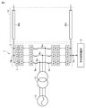
- FIG. 11 is a diagram showing a configuration example of the STATCOM of the ⁇ connection system.
- STATCOM 60 has a configuration in which arm circuits 61, 62, and 63 formed of a plurality of converter cells 7 connected in cascade with each other are delta-connected. Each arm circuit 61, 62, 63 may be provided with a reactor 64 in series with the converter cell 7.
- the STATCOM 60 is connected via a transformer 65 to a transmission line 66 provided in the AC circuit 12 (AC power system).
- Each of converter cells 7 forming arm circuits 61, 62, 63 has the configuration described in FIG. 9 of the second embodiment. Therefore, switching elements 35A, 35B, 41A, 41B constituting lower arms (i.e., second arm 34 and fourth arm 40) of full bridge type bridge circuit 30A are used instead of the conventional bypass switch. Can reduce the volume and cost of the converter cell 7.
- the switching elements 32A, 32B, 38A, 38B constituting the upper arm that is, the first arm 31 and the third arm 37
- the half bridge type bridge circuit 30 described in FIG. 6 may be used, or the streak outdoor type bridge circuit 30B described in FIG. 10 may be used.
- Y connection may be employed instead of the ⁇ connection shown in FIG. 11, or another connection method may be used.
Landscapes
- Engineering & Computer Science (AREA)
- Power Engineering (AREA)
- Inverter Devices (AREA)
Abstract
電力変換装置は、互いにカスケード接続された複数の変換器セル(7)を備える。各変換器セル(7)において、ブリッジ回路(30)を構成する複数のアーム(31;34)の各々には複数の半導体スイッチング素子(32A,32B;35A,35B)が並列に設けられている。各変換器セル(7)の駆動制御部(50)は、予め定める複数の異常モードをいずれも検出していない場合には、外部から与えられた指令に従って、ブリッジ回路(30)を制御するように構成される。駆動制御部(50)は、複数の異常モードの少なくとも1つを検出した場合には、ブリッジ回路(30)を構成する複数のアーム(31,34)のうち少なくとも1つ(34)に設けられた全ての半導体スイッチング素子(35A,35B)をオン状態にすることによって、第1および第2の入出力ノード(25p、25n)間を短絡するように構成される。
Description
本開示は、複数の変換器セルがカスケードに接続されることによって構成された自励式の電力変換装置に関し、たとえば、高圧直流送電、周波数変換器、無効電力補償装置などに好適に用いられるものである。
電力系統に接続される大容量の電力変換装置としてモジュラーマルチレベル変換器(MMC:Modular Multilevel Converter)が知られている。モジュラーマルチレベル変換器は、交流の各相に、高電位側直流端子に接続された上アーム(arm)回路と低電位側直流端子に接続された下アーム回路とを有する。各アーム回路は、多数の変換器セルがカスケードに接続されることによって構成されている。以下では、変換器セルをサブモジュールとも称する。
変換器セルは、エネルギー蓄積器としてのコンデンサと、第1および第2の入出力ノードと、これらの入出力ノードとコンデンサとの間を接続または非接続に切替えるためのブリッジ回路とを備える。ブリッジ回路として、ハーフブリッジ型またはフルブリッジ型などが用いられる。
MMCの各アーム回路を構成するいずれか1つの変換器セルが何らかの原因で故障すると、MMC全体が正常に動作しなくなる。このような、不都合を避けるために各変換器セルと並列にバイパススイッチが設けられている(たとえば、国際公開第2014/148100号(特許文献1)の段落0003参照)。変換器セルが故障した場合には、並列接続されたバイパススイッチをオンさせることによって当該変換器セルの出力を短絡する。これによって、MMCの運転を継続することができる。
本願の発明者らは、変換器セルを構成するブリッジ回路の各アームに半導体スイッチング素子を2個以上並列に設けることによって、電流容量を増大したMMCの開発を進めている。このような構成のMMCにおいて、さらに、上記文献のようなバイパススイッチを設けると、変換器セルの容積が増大するとともにコストの増加を招く。
本開示は、上記の問題点を考慮したものであり、その目的は、セル変換器の容積とコストを抑制すること可能な電力変換装置を提供することである。
一実施形態の電力変換装置は、互いにカスケード接続された複数の変換器セルを備える。各変換器セルは、第1の入出力ノードと、第2の入出力ノードと、エネルギー蓄積器と、ブリッジ回路と、駆動制御部とを含む。ブリッジ回路は、第1および第2の入出力ノードとエネルギー蓄積器との間の接続および非接続を切り替えるために設けられる。ブリッジ回路を構成する複数のアームのうち、半導体スイッチング素子が設けられているアームの各々には複数の半導体スイッチング素子が並列に設けられている。駆動制御部は、予め定める複数の異常モードをいずれも検出していない場合には、外部から与えられた指令に従って、ブリッジ回路を制御するように構成される。駆動制御部は、複数の異常モードの少なくとも1つを検出した場合には、ブリッジ回路を構成する複数のアームのうち少なくとも1つに設けられた全ての半導体スイッチング素子をオン状態にすることによって、第1および第2の入出力ノード間を短絡するように構成される。
上記の実施形態によれば、従来のバイパススイッチに代えて、ブリッジ回路を構成する半導体スイッチング素子を用いることができるので、セル変換器の容積とコストを抑制することができる。なお、上記の実施形態において、ブリッジ回路の各アームには複数の半導体スイッチング素子が並列に設けられているので、これらの複数の半導体スイッチング素子が全て同時に開放故障する可能性は低い。
以下、各実施の形態について図面を参照して詳しく説明する。なお、同一または相当する部分には同一の参照符号を付して、その説明を繰返さない。
実施の形態1.
[電力変換装置の概略構成]
図1は、実施の形態1の電力変換装置の概略的な構成例を示す図である。図1を参照して、電力変換装置1は、主回路であるレグ回路4u,4v,4w(不特定のものを示す場合、レグ回路4と記載する)と、中央制御装置3とを備える。本実施の形態では、レグ回路4u,4v,4wの全体を電力変換回路部2と称する。
[電力変換装置の概略構成]
図1は、実施の形態1の電力変換装置の概略的な構成例を示す図である。図1を参照して、電力変換装置1は、主回路であるレグ回路4u,4v,4w(不特定のものを示す場合、レグ回路4と記載する)と、中央制御装置3とを備える。本実施の形態では、レグ回路4u,4v,4wの全体を電力変換回路部2と称する。
レグ回路4は、交流を構成する複数相の各相に設けられ、交流回路12と直流回路14との間に接続されることにより、両回路間で電力変換を行う。図1には交流回路12が三相交流の場合が示され、u相、v相、w相にそれぞれ対応して3個のレグ回路4u,4v,4wが設けられている。
レグ回路4u,4v,4wにそれぞれ設けられた交流端子Nu,Nv,Nwは、連系変圧器13を介して交流回路12に接続される。交流回路12は、たとえば、交流電源などを含む交流電力系統である。図1では、図解を容易にするために、交流端子Nv,Nwと連系変圧器13との接続は図示していない。
各レグ回路4に共通に設けられた直流端子Np,Nn(すなわち、高電位側直流端子Np,低電位側直流端子Nn)は、直流回路14に接続される。直流回路14は、後述する図4の高圧直流送電(HVDC:High Voltage Direct Current)システムにおける直流電力系統、または図5のBTB(Back To Back)システムにおける他の電力変換装置との接続端子に相当する。
図1の連系変圧器13を用いる代わりに、連系リアクトルを介して交流回路12に接続した構成としても良い。また、図2および図3に示すように、交流回路12と各レグ回路4は、交流的に接続されていてもよい。この場合の交流回路12と各レグ回路4との接続部の詳細な構成については後述する。
レグ回路4uは、高電位側直流端子Npから交流端子Nuまでの上アーム回路5と、低電位側直流端子Nnから交流端子Nuまでの下アーム回路6とに区分される。上アーム回路5と下アーム回路6との接続点(すなわち、交流端子Nu)が変圧器13と接続される。また、高電位側直流端子Npおよび低電位側直流端子Nnが直流回路14に接続される。レグ回路4v,4wについても同様の構成を有しているので、以下、レグ回路4uを代表として説明する。
上アーム回路5は、カスケード接続された複数の変換器セル7と、リアクトル8pとを含む。複数の変換器セル7およびリアクトル8pは互いに直列接続されている。以下、簡単のために変換器セル7をセル7と称する場合がある。
同様に、下アーム回路6は、カスケード接続された複数のセル7と、リアクトル8nとを含む。複数のセル7およびリアクトル8nは互いに直列接続されている。
リアクトル8p,8nは、レグ回路中のセルがオンもしくはオフとなって出力電圧が急激に変化する瞬間に、または交流回路12または直流回路14などの事故時に、アーム電流Ipu,Ipnが急激に変化しないように設けられている。リアクトル8pが挿入される位置は、レグ回路4uの上アーム回路5のいずれの位置であってもよく、リアクトル8nが挿入される位置は、レグ回路4uの下アーム回路6のいずれの位置であってもよい。リアクトル8p,8nはそれぞれ複数個あってもよい。各リアクトルのインダクタンス値は互いに異なっていてもよい。さらに、上アーム回路5のリアクトル8pのみ、もしくは、下アーム回路6のリアクトル8nのみを設けてもよい。
図1の電力変換装置1は、さらに、制御に使用される電気量(電流、電圧など)を計測する検出器として、交流電圧検出器10と、交流電流検出器16と、直流電圧検出器11p,11nと、各レグ回路4に設けられたアーム電流検出器9p,9nとを含む。
具体的に、交流電圧検出器10は、交流回路12のU相、V相、W相の各相の電圧値を検出する。交流電流検出器16は、交流回路12のU相、V相、W相の各相の電流値Iacu,Iacv,Iacwを検出する。直流電圧検出器11pは、直流回路14に接続された高電位側直流端子Npの電圧を検出する。直流電圧検出器11nは、直流回路14に接続された低電位側直流端子Nnの電圧を検出する。
また、U相用のレグ回路4uに設けられたアーム電流検出器9p,9nは、上アーム回路5に流れるアーム電流Ipuおよび下アーム回路6に流れるアーム電流Inuをそれぞれ検出する。同様に、V相用のレグ回路4vに設けられたアーム電流検出器9p,9nは、上アーム電流Ipvおよび下アーム電流Invをそれぞれ検出する。W相用のレグ回路4wに設けられたアーム電流検出器9p,9nは、上アーム電流Ipwおよび下アーム電流Inwをそれぞれ検出する。これらのアーム電流に基づいて、直流回路14を流れる直流電流Idcおよび各レグ回路間を循環する循環電流を計算することができる。
上記の検出器によって検出された信号は、中央制御装置3に入力される。中央制御装置3は、さらに、各セル7からセルキャパシタ電圧の検出値を表す信号を受信する。中央制御装置3は、上記の各検出器の検出信号とセルキャパシタ電圧の情報とに基づいて、各セル7の運転状態を制御するための制御指令ならびに各セル7を保護するための運転/停止指令(運転指令または停止指令)を各セル7に出力する。
なお、図1では図解を容易にするために、各検出器から中央制御装置3に入力される信号の信号線ならびに中央制御装置3と各セル7との間で伝送される信号の信号線は一部まとめて記載されているが、実際には検出器ごとおよびセル7ごとに個別に設けられている。各セル7と中央制御装置3との間の信号線は、送信用と受信用とが別個に設けられていてもよい。また、本実施の形態の場合、これらの信号線は耐ノイズ性の観点から光ファイバによって構成される。
図1には示していないが、各アーム回路5,6には複数のバイパス回路が設けられていてもよい。この場合、各アーム回路を構成する複数の変換器セル7は、複数のブロックに区分され、ブロックごとにバイパス回路が設けられる。バイパス回路は、直流回路の故障時に故障電流を流すことによって電力変換回路部2を保護するためのものであり、たとえば、低電位側直流端子Nnから高電位側直流端子Npの方向が順方向となるように直列に接続されたダイオードによって構成されている。
バイパス回路は、背景技術で説明したバイパススイッチとは異なる点に注意すべきである。既に説明したように、バイパススイッチは、変換器セル7自身の故障時に変換器セル7の出力端子間を短絡させるために設けられる。本実施の形態の電力変換装置1は各変換器セル7の入出力端子間にバイパススイッチが接続されていない点に特徴がある。
[交流回路と各レグ回路との接続部の変形例]
図1では、レグ回路4u,4v,4wにそれぞれ設けられた交流端子Nu,Nv,Nwを介して、交流回路12と電力変換回路部2とが直流的に接続される例を示した。これに代えて、交流回路12と各レグ回路4は、変圧器を介して交流的に接続されていてもよい。以下、図2および図3を参照していくつかの具体例を説明する。
図1では、レグ回路4u,4v,4wにそれぞれ設けられた交流端子Nu,Nv,Nwを介して、交流回路12と電力変換回路部2とが直流的に接続される例を示した。これに代えて、交流回路12と各レグ回路4は、変圧器を介して交流的に接続されていてもよい。以下、図2および図3を参照していくつかの具体例を説明する。
図2は、交流回路と各レグ回路との接続部の変形例を示す図である。図2を参照して、交流回路12とレグ回路4u,4v,4wとは、三相変圧器80Bを介して接続される。
図2に示すように、三相変圧器80Bでは、一次巻線81u,81v,81wがΔ結線されている。具体的に、三相変圧器80Bの一次巻線81uは、交流回路12のU相とV相の間に接続される。三相変圧器80Bの一次巻線81vは、交流回路12のV相とW相との間に接続される。三相変圧器80Bの一次巻線81wは、交流回路12のW相とU相との間に接続される。
三相変圧器80Bの二次巻線82u,82v,82wは、それぞれ共通の鉄心を介して一次巻線81u,81v,81wと磁気結合する。さらに、二次巻線82uはU相のアーム回路5u,6uと直列に接続され、二次巻線82vはV相のアーム回路5v,6vと直列に接続され、二次巻線82wはW相のアーム回路5w,6wと直列に接続される。
図2の場合、二次巻線82u,82v,82wの各々は、各相のリアクトル8p,8nを兼ねている。リアクトル8p,8nとは別に三相変圧器80Bの二次巻線82u,82v,82wを設けてもよい。
なお、鉄心内に生じる直流磁束は、Δ結線された一次巻線81u,81v,81wに直流成分を流すことによって打ち消すことができる。
図3は、交流回路と各レグ回路との接続部の他の変形例を示す図である。図3を参照して、交流回路12とレグ回路4u,4v,4wとは、3巻線の三相変圧器80Cを介して接続される。
具体的に、図3の三相変圧器80Cの一次巻線81u,81v,81wの各一端は、交流回路12のU相、V相、W相の各送電線と連系変圧器13を介してそれぞれ接続される。三相変圧器80Cの一次巻線81u,81v,81wの各他端は共通の中性点84と接続される。すなわち、図3の場合、一次巻線81u,81v,81wはY結線されている。
三相変圧器80Cの二次巻線82u,82v,82wは、それぞれ共通の鉄心を介して一次巻線81u,81v,81wと磁気結合する。図3の三相変圧器80Cでは、さらに、二次巻線82u,82v,82wとそれぞれ直列に接続された三次巻線83u,83v,83wが設けられている。各相の二次巻線と対応する三次巻線とは逆極性になるように接続され、共通の鉄心に巻回される。また、各相の二次巻線と対応する三次巻線との接続点は共通の中性点85に接続される。
さらに、二次巻線82uおよび三次巻線83uはU相のアーム回路5u,6uと直列に接続される。二次巻線82vおよび三次巻線83vはV相のアーム回路5v,6vと直列に接続される。二次巻線82wおよび三次巻線83wはW相のアーム回路5w,6wと直列に接続される。図3の場合、二次巻線82u,82v,82wの各々および三次巻線83u,83v,83wの各々は、各相のリアクトル8p,8nを兼ねている。リアクトル8p,8nとは別に三相変圧器80Cの二次巻線82u,82v,82wおよび三次巻線83u,83v,83wを設けてもよい。
図3の三相変圧器80Cによれば、各相のアーム電流(U相:Ipu,Inu、V相:Ipv,Inv、W相:Ipw,Inw)によって二次巻線に生じる直流起電力と三次巻線に生じる起電力とは互いに打ち消し合うため、鉄心内に直流磁束が生じないというメリットがある。
[HVDCシステムの構成例]
図4は、図1の電力変換装置を利用したHVDCシステムの概略的な構成例を示す図である。
図4は、図1の電力変換装置を利用したHVDCシステムの概略的な構成例を示す図である。
HVDC(高圧直流送電:High Voltage Direct Current)システムは、高電圧の交流電力を直流電力に変換してから直流長距離送電を行うものである。図4に示すように、交流/直流変換に、図1で説明した電力変換装置1が利用される。電力変換装置1の高電位側直流端子Npは高電位側の送電線20pに接続され、電力変換装置1の低電位側直流端子Nnは低電位側の送電線20nに接続される。送電線20p,20nを含む直流電力系統が図1の直流回路14に相当する。
図4のHVDCシステムの構成は一例であって、この例に限定されるわけではない。たとえば、交流回路12と各レグ回路4との接続部は、図2および図3で説明したような三相変圧器80B,80Cであってもよい。
[BTBシステムの構成例]
図5は、図1の電力変換装置を利用したBTBシステムの概略的な構成例を示す図である。
図5は、図1の電力変換装置を利用したBTBシステムの概略的な構成例を示す図である。
BTB(Back To Back)システムは、交流を直流に変換する順変換と、直流を交流に変換する逆変換とを行うことによって、2つの交流回路間で電力融通を行うものである。順変換および逆変換に図1で説明した電力変換装置1が利用される。
具体的に図5を参照して、BTBシステム70は、高電位側直流端子Npおよび低電位側直流端子Nnを互いに共有する電力変換回路部2A,2Bと、電力変換回路部2A,2Bを制御する中央制御装置3とを備える。電力変換回路部2Aの交流端子Nu,Nv,Nwは連系変圧器13Aを介在して交流回路12A(交流電力系統)と接続される。電力変換回路部2Bの交流端子Nu,Nv,Nwは連系変圧器13Bを介在して交流回路12B(交流電力系統)と接続される。電力変換回路部2A,2Bによって共有されている高電位側直流端子Npおよび低電位側直流端子Nnが電力変換装置1の直流回路14に相当する。
図5のBTBシステム70の構成は一例であって、この例に限定されるわけではない。たとえば、交流回路12Aと電力変換回路部2Aの各レグ回路との接続部および交流回路12Bと電力変換回路部2Bの各レグ回路との接続部は、図2および図3で説明したような三相変圧器80B,80Cであってもよい。
[変換器セルの構成]
図6は、図1の各レグ回路を構成する変換器セルの一例を示す図である。図6に示す変換器セル7は、第1の入出力ノード25pと、第2の入出力ノード25nと、ハーフブリッジ型のブリッジ回路30と、エネルギー蓄積器としての直流コンデンサ47と、駆動制御部50と、電圧検出器48と、ラッチ型のスイッチ58と、電池59とを備える。電池59をバッテリ電源部とも称する。
図6は、図1の各レグ回路を構成する変換器セルの一例を示す図である。図6に示す変換器セル7は、第1の入出力ノード25pと、第2の入出力ノード25nと、ハーフブリッジ型のブリッジ回路30と、エネルギー蓄積器としての直流コンデンサ47と、駆動制御部50と、電圧検出器48と、ラッチ型のスイッチ58と、電池59とを備える。電池59をバッテリ電源部とも称する。
入出力ノード25pは、高電位側直流端子Npに近い側において隣接する変換器セル7の入出力ノード25nと接続される。最も高電位側直流端子Npに近接して配置された変換器セル7の入出力ノード25pは、高電位側直流端子Npと接続される。同様に、入出力ノード25nは、低電位側直流端子Nnに近い側で隣接する変換器セル7の入出力ノード25pと接続される。最も低電位側直流端子Nnに近接して配置された変換器セル7の入出力ノード25nは、低電位側直流端子Nnと接続される。
ハーフブリッジ型のブリッジ回路30は、直流コンデンサ47の正極側のノード45と入出力ノード25pとの間に接続された第1アーム31と、直流コンデンサ47の負極側のノード46と入出力ノード25pとの間に接続された第2アーム34とを含む。入出力ノード25nはノード46と直接接続される。
第1アーム31は、互いに並列に接続された半導体スイッチング素子32A,32B(以下、単にスイッチング素子と称する場合がある)と、ダイオード33A,33Bとを含む。ダイオード33A,33Bは、スイッチング素子32A,32Bとそれぞれ逆並列(すなわち、並列かつ逆バイアス方向)に接続される。同様に、第2アーム34は、互いに並列に接続された半導体スイッチング素子35A,35Bと、ダイオード36A,36Bとを含む。ダイオード36A,36Bは、スイッチング素子35A,35Bとそれぞれ逆並列に接続される。
図6では、ブリッジ回路30の各アームに2個の半導体スイッチング素子が並列に設けられている場合を示しているが、各アームには2個より多い半導体スイッチング素子が並列に設けられていてもよい。
半導体スイッチング素子32A,32B,35A,35Bとして、たとえば、IGBT(Insulated Gate Bipolar Transistor)またはGCT(Gate Commutated Turn-off thyristor)などの自励式の半導体スイッチング素子が用いられる。
電圧検出器48は、直流コンデンサ47に保持された直流電圧を検出する。直流コンデンサ47は、たとえば、直流計器用電圧変成器(DCVT:Direct Current Voltage Transformer)である。以下の説明では、直流コンデンサ47の電圧をセルキャパシタ電圧とも称する。
駆動制御部50は、電源回路51と、制御ロジック52と、駆動回路53と、通信回路54とを含む。これらの各要素は、別々の回路基板上に形成されていてもよいし、少なくとも一部の要素が共通する回路基板上に形成されてもよい。制御ロジック52は、専用回路として構成されていてもよいし、FPGA(Field Programmable Gate Array)を利用して構成されていてもよい。もしくは、制御ロジック52の機能を、CPU(Central Processing Unit)およびメモリなどを備えたマイクロコンピュータによって実現してもよい。
電源回路51は、直流コンデンサ47に蓄えられた電圧に基づいて、変換器セル7内の制御ロジック52、駆動回路53、および通信回路54などで使用される種々の大きさの駆動電圧を生成する。したがって、電力変換装置1の起動時に直流コンデンサ47に電荷が蓄積されると初めて電源回路51が動作し、これによって駆動制御部50を構成するその他の回路が動作することになる。
通信回路54は、中央制御装置3に設けられた通信回路との間で通信を行う。この通信には耐ノイズ性の観点から光ファイバが用いられる。駆動回路53は、制御ロジック52からのオンオフ指令に基づいて、半導体スイッチング素子32A,32B,35A,35Bのゲート駆動信号を生成する。
制御ロジック52は、通信回路54を介して中央制御装置3から受けた制御指令および運転/停止指令に基づいて、半導体スイッチング素子32A,32B,35A,35Bのオンオフを制御する。制御ロジック52からのオンオフ信号は駆動回路53によって増幅されることによってゲート駆動信号が生成される。制御ロジック52は、さらに、電圧検出器48によって検出された直流コンデンサ47の電圧の情報を中央制御装置3に向けて送信する。
さらに、制御ロジック52は、図示しない複数のセンサを用いて、変換器セル7内の複数の異常モードを検知するように構成されている。たとえば、以下のような異常検出を行う。なお、異常モードは以下に限定されるものでない。
(i) 電圧検出器48によって検出された直流コンデンサ47の電圧が予め定める適正範囲内に入っているか否かが検出される。直流コンデンサ電圧が適正範囲よりも低い場合あるいは直流コンデンサ電圧が適正範囲よりも高い場合は、いずれかの半導体スイッチング素子32A,32B,35A,35Bのスイッチング動作が正しく行われていない故障が疑われる。
(ii) 通信回路54を介して通信が正常に行われているか否かが検出される。たとえば、中央制御装置3からの通信の停止、および中央制御装置3からの受信信号に含まれる誤り検出符号の誤りが検知される。
(iii) 電源回路51によって生成された電圧が設定電圧範囲内であるか否かが検出される。
(iv) 制御ロジック52から出力されたオンオフ指令と矛盾しない電圧が、駆動回路53から出力されているか否かが検出される。
制御ロジック52は、予め定める複数の異常モードのうち少なくとも1つを検出した場合には、第2アーム34を構成する半導体スイッチング素子35A,35Bを全てオンにする(すなわち、閉状態にする)ことによって、入出力ノード25p,25n間を短絡するように制御する。具体的には、制御ロジック52は、スイッチ58をオンする(すなわち、閉状態にする)ことによって電池59の出力電圧を半導体スイッチング素子35A,35Bのゲートに印加するようにする。なお、スイッチ58は、制御ロジック52からの駆動信号が供給されなくてもオン状態を維持するラッチ型のスイッチであることが望ましい。これによって、入出力ノード25p,25n間の短絡後に直流コンデンサ47の電圧が放電されることによって電源回路51が動作しなくなっても、半導体スイッチング素子35A,35Bのオン状態を維持することができる。
図6の変換器セル7は、入出力ノード25p,25n間を短絡するために従来必要であったバイパススイッチが設けられていない点に特徴がある。第2アーム34を構成する半導体スイッチング素子35A,35Bをオン状態にすることによって、従来バイパススイッチをオンしていたのと同一の効果を奏することができる。本実施形態の変換器セル7は、第2アーム34に2個の半導体スイッチング素子35A,35Bが並列で設けられているので、これらの半導体スイッチング素子35A,35Bが両方とも同時に故障する可能性はかなり低い。このため、半導体スイッチング素子35A,35Bをバイパススイッチの代わりに用いることができる。また、半導体スイッチング素子35A,35Bの消費電力は主として導通損とスイッチング損失であり、半導体スイッチング素子35A,35Bを常時オン状態としたときにはスイッチング損がないので、消費電力は問題とならない。
なお、電力変換装置1を構成する各アーム回路5,6には、1個以上の冗長な変換器セル7が設けられている。これによって、異常モードにある変換器セル7の入出力ノード25p,25n間を短絡させたとしても電力変換装置1の動作上の問題とならないようにしている。
[変換器セルおよび電力変換装置の動作]
次に、変換器セル7の動作と、変換器セル7の異常モードに関連する電力変換装置1の動作について説明する。まず、変換器セル7の動作状態には、以下の3つの動作状態がある。
次に、変換器セル7の動作と、変換器セル7の異常モードに関連する電力変換装置1の動作について説明する。まず、変換器セル7の動作状態には、以下の3つの動作状態がある。
(1) 変換器セル7の異常モードが検出されておらず、かつ、中央制御装置3から制御指令を受けている場合。
この場合、制御ロジック52は、中央制御装置3から受けた制御指令に従って、第1アーム31および第2アーム34の一方が導通して他方が非導通となるように、半導体スイッチング素子32A,32B,35A,35Bを制御する。たとえば、制御指令は、アームごとの電圧指令値であり、各変換器セル7は電圧指令値に応じて零電圧またはセルキャパシタ電圧を出力するように半導体スイッチング素子32A,32B,35A,35Bを制御する。
具体的に、第1アーム31を構成するスイッチング素子32A,32Bがオン状態であり、第2アーム34を構成するスイッチング素子35A,35Bがオフ状態のとき、入出力ノード25p,25n間には直流コンデンサ47の両端間の電圧が印加される。逆に、第1アーム31を構成するスイッチング素子32A,32Bがオフ状態であり、第2アーム34を構成するスイッチング素子35A,35Bがオン状態のとき、入出力ノード25p,25n間は0Vとなる。
したがって、図6に示す変換器セル7は、第1アーム31を構成するスイッチング素子32A,32Bと第2アーム34を構成するスイッチング素子35A,35Bとを交互にオン状態とすることによって、零電圧または直流コンデンサ47の電圧に依存した正電圧を出力することができる。
(2) 変換器セル7の異常モードが検出されておらず、かつ、中央制御装置3から停止指令を受けている場合。
たとえば、図1の中央制御装置3は、アーム電流の過電流を検出した場合には、各変換器セル7に停止指令を出力する。この場合、制御ロジック52は、回路保護のために第1アーム31および第2アーム34を構成する全ての半導体スイッチング素子32A,32B,35A,35Bをオフにする。
(3) 変換器セル7の異常モードが検出されている場合。この場合、制御ロジック52は、スイッチ58をオンする(すなわち、閉状態にする)ことによって電池59の出力電圧を半導体スイッチング素子35A,35Bに印加するようにする。この結果、第2アーム34を構成する半導体スイッチング素子35A,35Bが全てオン状態になり、これによって入出力ノード25p,25n間が短絡される。
図7は、変換器セルの動作を示すフローチャートである。以下、図6および図7を参照してこれまでの説明を総括する。
制御ロジック52は、変換器セル7の複数の異常モードをいずれも検出していない場合には(ステップS120でNO)、ステップS100において、中央制御装置3からの制御指令および運転/停止指令に従って、各半導体スイッチング素子32A,32B,35A,35Bを制御する。さらに、この場合、制御ロジック52は、ステップS110において、直流コンデンサ47の電圧検出値の情報を中央制御装置3に向けて送信する。
一方、制御ロジック52は、変換器セル7の複数の異常モードの少なくとも1つを検出した場合には(ステップS120でNO)、ステップS130において、ブリッジ回路30を構成する下側のアーム34に設けられた全てのスイッチング素子をオン状態にすることによって、第1および第2の入出力ノード25p,25n間を短絡する。これによって、故障セル以外の変換器セルを用いてMMCの運転を継続することができる。
なお、第1および第2の入出力ノード25p,25n間を短絡するために、どのアームの全スイッチング素子をオン状態にするかは、ブリッジ回路の構成に応じて異なる場合があることに注意しなければならない。たとえば、後述する図9のフルブリッジ型の場合には、下側の第2アーム34および第4アーム40の全スイッチング素子をオン状態にしてもよいし、上側の第1アーム31および第3アーム37の全スイッチング素子をオン状態にしてもよい。したがって、より一般的には、制御ロジック52は、変換器セル7の複数の異常モードの少なくとも1つを検出した場合には(ステップS120でNO)、ブリッジ回路を構成する複数のアームのうち第1および第2の入出力ノード25p,25n間を短絡するのに必要である、少なくとも1つのアームの全スイッチング素子をオン状態にする。
次に、各変換器セル7の異常モードに関連した電力変換装置1の制御について説明する。既に説明したように、電力変換装置1を構成する各アーム回路5,6には、予め定める数の冗長な変換器セル7が設けられている。
図8は、異常モードの検出に関連した中央制御装置の動作を示すフローチャートである。図1、図6、および図8を参照して、ステップS200において、中央制御装置3は、アーム回路ごとに故障セル数(すなわち、異常モードを検出したために、入出力ノード25p,25n間が短絡状態となっているセルの数)に関する情報を取得する。
次のステップS210において、中央制御装置3は、初期状態の冗長セル数から故障セル数を減じることによって、現時点の冗長セル数を計算する。そして、中央制御装置3は、現時点の冗長セル数が0より小さい場合、すなわち、故障セル数が冗長セル数の初期値を上回った場合には(ステップS220でYES)、ステップS240において電力変換装置1の動作を停止する。具体的には、交流回路12との間の交流遮断器(不図示)と、直流回路14との間の直流遮断器(不図示)との両方を開放状態にするとともに、電力変換回路部2を構成する各変換器セル7に設けられた半導体スイッチング素子32A,32B,35A,35Bが全てオフ状態になるように各変換器セル7を制御する。
一方、現時点の冗長セル数が0以上の場合には(ステップS220でNO)、ステップS230において、中央制御装置3は、現時点の冗長セルと故障セルを除いた変換器セル7によって各アーム回路5,6を動作させる。この場合、中央制御装置3は、現時点の冗長セルに対して第2アーム34を構成するスイッチング素子35A,35Bが常にオン状態となるように制御指令を出力してもよい。もしくは、中央制御装置3は、現時点の冗長セル数と故障セル数を除いた有効セル数(有効セル数は、故障セル数に関係なく一定である)に対応した電圧指令値を、制御指令として各アーム回路5,6に出力するようにしてもよい。この電圧指令値に基づいて、冗長セルに対応する変換器セル7の制御ロジック52は、第2アーム34を構成するスイッチング素子35A,35Bを常にオン状態にする。
[効果]
上記のとおり、実施の形態1の電力変換装置1によれば、各変換器セル7を構成するブリッジ回路30の各アームには2個以上の半導体スイッチング素子32が並列に設けられている。これによって、電力変換装置1の電流容量を増加させることができるとともに、バイパススイッチの代わりとして、ブリッジ回路30の下アーム(すなわち、第2アーム34)を構成するスイッチング素子35A,35Bを用いることができる。第2アーム34を構成するスイッチング素子35A,35Bが全て同時に故障する可能性は低いからである。この結果、変換器セル7の容積とコストを抑制することができる。
上記のとおり、実施の形態1の電力変換装置1によれば、各変換器セル7を構成するブリッジ回路30の各アームには2個以上の半導体スイッチング素子32が並列に設けられている。これによって、電力変換装置1の電流容量を増加させることができるとともに、バイパススイッチの代わりとして、ブリッジ回路30の下アーム(すなわち、第2アーム34)を構成するスイッチング素子35A,35Bを用いることができる。第2アーム34を構成するスイッチング素子35A,35Bが全て同時に故障する可能性は低いからである。この結果、変換器セル7の容積とコストを抑制することができる。
実施の形態2.
実施の形態1では、各変換器セル7はハーフブリッジ型のブリッジ回路30によって構成されていた。以下では、各変換器セル7がフルブリッジ型またはスリークオーター(Three Quarter)型のブリッジ回路によって構成される場合について説明する。いずれの回路構成であっても、実施の形態1の場合と同様の効果を奏する。以下では、実施の形態1と異なる点について主に説明し、共通する点については説明を繰り返さない。
実施の形態1では、各変換器セル7はハーフブリッジ型のブリッジ回路30によって構成されていた。以下では、各変換器セル7がフルブリッジ型またはスリークオーター(Three Quarter)型のブリッジ回路によって構成される場合について説明する。いずれの回路構成であっても、実施の形態1の場合と同様の効果を奏する。以下では、実施の形態1と異なる点について主に説明し、共通する点については説明を繰り返さない。
[フルブリッジ型のブリッジ回路の構成]
図9は、図1の各レグ回路を構成する変換器セルの他の構成例を示す図である。図9の変換器セル7は、ハーフブリッジ型のブリッジ回路30に代えてフルブリッジ型のブリッジ回路30Aが設けられている点で図6の変換器セル7と異なる。以下では、図6のブリッジ回路30と異なる点について主に説明し、図6の場合と共通する点については同一の参照符号を付して説明を繰り返さない。
図9は、図1の各レグ回路を構成する変換器セルの他の構成例を示す図である。図9の変換器セル7は、ハーフブリッジ型のブリッジ回路30に代えてフルブリッジ型のブリッジ回路30Aが設けられている点で図6の変換器セル7と異なる。以下では、図6のブリッジ回路30と異なる点について主に説明し、図6の場合と共通する点については同一の参照符号を付して説明を繰り返さない。
図9の変換器セル7は、第1の入出力ノード25pと、第2の入出力ノード25nと、フルブリッジ型のブリッジ回路30Aと、エネルギー蓄積器としての直流コンデンサ47と、駆動制御部50と、電圧検出器48と、ラッチ型のスイッチ58A,58Bと、電池59A,59Bとを備える。
以下では、電池59A,59Bをまとめてバッテリ電源部と称する。バッテリ電源部は、上記のように2つの電池59A,59Bによって構成されていてもよいし、単一の電池によって構成されていてもよい。
フルブリッジ型のブリッジ回路30Aは、正極側のノード45と入出力ノード25pとの間に接続された第1アーム31と、負極側のノード46と入出力ノード25pとの間に接続された第2アーム34と、正極側のノード45と入出力ノード25nとの間に接続された第3アーム37と、負極側のノード46と入出力ノード25nとの間に接続された第4アーム40とを含む。第1アーム31および第2アーム34の構成は、図6の場合と同様であるので説明を繰り返さない。
第3アーム37は、互いに並列に接続された半導体スイッチング素子38A,38Bと、ダイオード39A,39Bとを含む。ダイオード39A,39Bは、スイッチング素子38A,38Bとそれぞれ逆並列に接続される。同様に、第4アーム40は、互いに並列に接続された半導体スイッチング素子41A,41Bと、ダイオード42A,42Bとを含む。ダイオード42A,42Bは、スイッチング素子41A,41Bとそれぞれ逆並列に接続される。
図9では、ブリッジ回路30Aの各アームに2個の半導体スイッチング素子が並列に設けられている場合を示しているが、各アームには2個より多い半導体スイッチング素子が並列に設けられていてもよい。
制御ロジック52は、予め定める複数の異常モードのうち少なくとも1つを検出した場合には、第2アーム34を構成する半導体スイッチング素子35A,35Bを全てオンにするとともに、第4アーム40を構成する半導体スイッチング素子41A,41Bを全てにオンにする。これによって、入出力ノード25p,25n間が短絡される。具体的には、制御ロジック52は、スイッチ58Aをオンすることによって電池59Aの出力電圧を半導体スイッチング素子35A,35Bのゲートに印加するとともに、スイッチ58Bをオンすることによって電池59B(または、電池59Aと共通化された単一の電池)の出力電圧を半導体スイッチング素子41A,41Bのゲートに印加する。
図9の変換器セル7は、入出力ノード25p,25n間を短絡するために従来必要であったバイパススイッチが設けられていない点に特徴がある。第2アーム34を構成する全ての半導体スイッチング素子35A,35Bをオン状態にするとともに第4アーム40を構成する全ての半導体スイッチング素子41A,41Bをオン状態にすることによって、従来バイパススイッチをオン状態にしていたのと同一の効果を得ることができる。本実施形態の変換器セル7は、第2アーム34および第4アーム40のいずれにも2個の半導体スイッチング素子が並列で設けられているので、これら2個の半導体スイッチング素子が両方とも同時に故障する可能性はかなり低い。このため、半導体スイッチング素子をバイパススイッチの代わりにすることができる。
なお、第2アーム34および第4アーム40に代えて、第1アーム31および第3アーム37を構成する全てのスイッチング素子をオン状態となるように制御することによっても、入出力ノード25p,25n間を短絡することができる。
[スリークオーター型のブリッジ回路の構成]
図10は、図1の各レグ回路を構成する変換器セルのさらに他の構成例を示す図である。図10の変換器セル7は、フルブリッジ型のブリッジ回路30Aに代えてスリークオーター型のブリッジ回路30Bが設けられている点で、図9の変換器セル7と異なる。
図10は、図1の各レグ回路を構成する変換器セルのさらに他の構成例を示す図である。図10の変換器セル7は、フルブリッジ型のブリッジ回路30Aに代えてスリークオーター型のブリッジ回路30Bが設けられている点で、図9の変換器セル7と異なる。
具体的に、図10のスリークオーター型のブリッジ回路30Bは、図9のフルブリッジ型のブリッジ回路30Aと比べて第3アームの構成が異なる。より詳細には、図10の第3アーム37Aは、図9の第3アーム37から半導体スイッチング素子38A,38Bを除去した構成である。図10のその他の構成は図9の場合と同様であり、同一または相当する部分には同一の参照符号を付して説明を繰り返さない。
なお、電力変換装置1を構成する各アーム回路5,6は、ハーフブリッジ型の変換器セル7、フルブリッジ型の変換器セル7、およびスリークオーター型の変換器セル7のうちいずれか2種類または3種類とも混在したものであってもよい。
実施の形態3.
実施の形態3では、実施の形態1で説明した電力変換装置をSTATCOM(Static Synchronous Compensator)と称する無効電力補償装置に適用した例について説明する。
実施の形態3では、実施の形態1で説明した電力変換装置をSTATCOM(Static Synchronous Compensator)と称する無効電力補償装置に適用した例について説明する。
図11は、Δ結線方式のSTATCOMの構成例を示す図である。図11を参照して、STATCOM60は、互いにカスケードに接続された複数の変換器セル7からなるアーム回路61,62,63がデルタ結線された構成を有している。各アーム回路61,62,63には、変換器セル7と直列にリアクトル64が設けられていてもよい。STATCOM60は、変圧器65を介して交流回路12(交流電力系統)に設けられた送電線66と接続される。
アーム回路61,62,63を構成する変換器セル7の各々は、実施の形態2の図9で説明した構成を有している。したがって、従来のバイパススイッチの代わりに、フルブリッジ型のブリッジ回路30Aの下側のアーム(すなわち、第2アーム34および第4アーム40)を構成するスイッチング素子35A,35B,41A,41Bを用いることができるので、変換器セル7の容積およびコストを抑制することができる。なお、フルブリッジ型のブリッジ回路30Aの場合、上側のアーム(すなわち、第1アーム31および第3アーム37)を構成するスイッチング素子32A,32B,38A,38Bを、従来のバイパススイッチの代わりに用いてもよい。
図9のフルブリッジ型のブリッジ回路30Aに代えて、図6で説明したハーフブリッジ型のブリッジ回路30を用いてもよいし、図10で説明したスリークオーター型のブリッジ回路30Bを用いてもよい。また、アーム回路の接続に関して、図11に示したΔ結線に変えてY結線にしてもよいし、他の接続方式を用いてもよい。
今回開示された実施の形態はすべての点で例示であって制限的なものでないと考えられるべきである。この発明の範囲は上記した説明ではなくて請求の範囲によって示され、請求の範囲と均等の意味および範囲内でのすべての変更が含まれることが意図される。
1 電力変換装置、3 中央制御装置、4,4u,4v,4w レグ回路、5,6,61,62,63 アーム回路、7 変換器セル、8n,8p,64 リアクトル、12,12A,12B 交流回路、14 直流回路、25n 第2の入出力ノード、25p 第1の入出力ノード、30,30A,30B ブリッジ回路、31,34,37,40 アーム、32A,32B,35A,35B,38A,38B,41A,41B 半導体スイッチング素子、47 直流コンデンサ、48 電圧検出器、50 駆動制御部、51 電源回路、52 制御ロジック、53 駆動回路、54 通信回路、58,58A,58B スイッチ、59,59A,59B 電池、80B,80C 三相変圧器、Nn 低電位側直流端子、Np 高電位側直流端子、Nu,Nv,Nw 交流端子。
Claims (13)
- 互いにカスケード接続された複数の変換器セルを備え、
各前記変換器セルは、
第1の入出力ノードと、
第2の入出力ノードと、
エネルギー蓄積器と、
前記第1および第2の入出力ノードと前記エネルギー蓄積器との間の接続および非接続を切り替えるためのブリッジ回路とを含み、
前記ブリッジ回路を構成する複数のアームのうち、半導体スイッチング素子が設けられているアームの各々には複数の半導体スイッチング素子が並列に設けられており、
各前記変換器セルは、駆動制御部をさらに含み、
前記駆動制御部は、予め定める複数の異常モードをいずれも検出していない場合には、外部から与えられた指令に従って、前記ブリッジ回路を制御するように構成され、
前記駆動制御部は、前記複数の異常モードの少なくとも1つを検出した場合には、前記ブリッジ回路を構成する複数のアームのうち少なくとも1つに設けられた全ての半導体スイッチング素子をオン状態にすることによって、前記第1および第2の入出力ノード間を短絡するように構成される、電力変換装置。 - 前記ブリッジ回路を構成する複数のアームのうち、半導体スイッチング素子が設けられているアームの各々には前記複数の半導体スイッチング素子として2個の半導体スイッチング素子が並列に設けられている、請求項1に記載の電力変換装置。
- 各前記変換器セルの前記第1の入出力ノードと前記第2の入出力ノードとの間には、前記ブリッジ回路を構成する半導体スイッチング素子以外のスイッチが設けられていない、請求項1または2に記載の電力変換装置。
- 前記複数の異常モードは、前記エネルギー蓄積器の電圧が予め定める範囲外となることを含む、請求項1~3のいずれか1項に記載の電力変換装置。
- 前記複数の異常モードは、前記駆動制御部と外部との通信が異常であることを含む、請求項1~4のいずれか1項に記載の電力変換装置。
- 前記駆動制御部は、前記エネルギー蓄積器に保持された電圧によって駆動電圧を生成する電源回路を含み、
前記複数の異常モードは、前記駆動電圧が設定範囲にないことを含む、請求項1~5のいずれか1項に記載の電力変換装置。 - 前記ブリッジ回路は、
前記エネルギー蓄積器の正極側ノードと前記第1の入出力ノードとの間に設けられた第1アームと、
前記エネルギー蓄積器の負極側ノードと前記第1の入出力ノードとの間に設けられた第2アームとを含み、
前記第2の入出力ノードは、前記エネルギー蓄積器の負極側ノードと直接接続され、
前記駆動制御部は、前記複数の異常モードの少なくとも1つを検出した場合には、前記第2アームを構成する全ての半導体スイッチング素子がオン状態になるように前記ブリッジ回路を制御する、請求項1~6のいずれか1項に記載の電力変換装置。 - 各前記変換器セルは、さらに、
バッテリ電源部と、
前記バッテリ電源部の出力と前記第2アームを構成する複数の半導体スイッチング素子のゲートとの間に接続された第1のラッチ型スイッチとを含み、
前記駆動制御部は、前記複数の異常モードの少なくとも1つを検出した場合には、前記第1のラッチ型スイッチをオンすることによって、前記第2アームを構成する全ての半導体スイッチング素子をオン状態にする、請求項7に記載の電力変換装置。 - 前記ブリッジ回路は、
前記エネルギー蓄積器の正極側ノードと前記第1の入出力ノードとの間に設けられた第1アームと、
前記エネルギー蓄積器の負極側ノードと前記第1の入出力ノードとの間に設けられた第2アームと、
前記エネルギー蓄積器の正極側ノードと前記第2の入出力ノードとの間に設けられた第3アームと、
前記エネルギー蓄積器の負極側ノードと前記第2の入出力ノードとの間に設けられた第4アームとを含み、
前記駆動制御部は、前記複数の異常モードの少なくとも1つを検出した場合には、前記第2アームおよび前記第4アームを構成する全ての半導体スイッチング素子がオン状態になるように前記ブリッジ回路を制御する、請求項1~6のいずれか1項に記載の電力変換装置。 - 各前記変換器セルは、さらに、
バッテリ電源部と、
前記バッテリ電源部の出力と前記第2アームを構成する複数の半導体スイッチング素子のゲートとの間に接続された第1のラッチ型スイッチと、
前記バッテリ電源部の出力と前記第4アームを構成する複数の半導体スイッチング素子のゲートとの間に接続された第2のラッチ型スイッチとを含み、
前記駆動制御部は、前記複数の異常モードの少なくとも1つを検出した場合には、前記第1のラッチ型スイッチをオンすることによって前記第2アームを構成する全ての半導体スイッチング素子をオン状態にするとともに、前記第2のラッチ型スイッチをオンすることによって前記第4アームを構成する全ての半導体スイッチング素子をオン状態にする、請求項9に記載の電力変換装置。 - 前記ブリッジ回路は、
前記エネルギー蓄積器の正極側ノードと前記第1の入出力ノードとの間に設けられた第1アームと、
前記エネルギー蓄積器の負極側ノードと前記第1の入出力ノードとの間に設けられた第2アームと、
前記エネルギー蓄積器の正極側ノードと前記第2の入出力ノードとの間に設けられた第3アームと、
前記エネルギー蓄積器の負極側ノードと前記第2の入出力ノードとの間に設けられた第4アームとを含み、
前記駆動制御部は、前記複数の異常モードの少なくとも1つを検出した場合には、前記第1アームおよび前記第3アームを構成する全ての半導体スイッチング素子がオン状態になるように前記ブリッジ回路を制御する、請求項1~6のいずれか1項に記載の電力変換装置。 - 前記電力変換装置は、各前記変換器セルに制御指令および運転/停止指令を送信する中央制御装置をさらに備え、
前記中央制御装置は、前記複数の異常モードのいずれかが検出されたことによって前記第1の入出力ノードと前記第2の入出力ノードとの間が短絡状態である故障セルの数の情報を取得し、
前記中央制御装置は、前記故障セルの数が予め定める閾値を超えた場合には、前記電力変換装置の動作を停止するように構成される、請求項1~11のいずれか1項に記載の電力変換装置。 - 請求項1~12のいずれか1項に記載の電力変換装置を備えた無効電力補償装置。
Priority Applications (4)
| Application Number | Priority Date | Filing Date | Title |
|---|---|---|---|
| US16/613,684 US10992219B2 (en) | 2017-06-27 | 2017-06-27 | Power conversion device |
| EP17915832.4A EP3648331A4 (en) | 2017-06-27 | 2017-06-27 | POWER CONVERSION DEVICE |
| PCT/JP2017/023496 WO2019003290A1 (ja) | 2017-06-27 | 2017-06-27 | 電力変換装置 |
| JP2017567479A JP6359213B1 (ja) | 2017-06-27 | 2017-06-27 | 電力変換装置 |
Applications Claiming Priority (1)
| Application Number | Priority Date | Filing Date | Title |
|---|---|---|---|
| PCT/JP2017/023496 WO2019003290A1 (ja) | 2017-06-27 | 2017-06-27 | 電力変換装置 |
Publications (1)
| Publication Number | Publication Date |
|---|---|
| WO2019003290A1 true WO2019003290A1 (ja) | 2019-01-03 |
Family
ID=62904849
Family Applications (1)
| Application Number | Title | Priority Date | Filing Date |
|---|---|---|---|
| PCT/JP2017/023496 Ceased WO2019003290A1 (ja) | 2017-06-27 | 2017-06-27 | 電力変換装置 |
Country Status (4)
| Country | Link |
|---|---|
| US (1) | US10992219B2 (ja) |
| EP (1) | EP3648331A4 (ja) |
| JP (1) | JP6359213B1 (ja) |
| WO (1) | WO2019003290A1 (ja) |
Cited By (3)
| Publication number | Priority date | Publication date | Assignee | Title |
|---|---|---|---|---|
| JP2021141799A (ja) * | 2020-03-04 | 2021-09-16 | 富士電機株式会社 | 電力変換装置 |
| JP2022129022A (ja) * | 2021-02-24 | 2022-09-05 | 東芝三菱電機産業システム株式会社 | 電力変換装置 |
| JP2023530866A (ja) * | 2020-06-29 | 2023-07-20 | マシイネンフアブリーク・ラインハウゼン・ゲゼルシヤフト・ミツト・ベシユレンクテル・ハフツング | セル集合体及びこのようセル集合体をそれぞれ有する複数のアームから成るコンバータ |
Families Citing this family (18)
| Publication number | Priority date | Publication date | Assignee | Title |
|---|---|---|---|---|
| CN108566101B (zh) * | 2016-12-16 | 2020-09-22 | 台达电子企业管理(上海)有限公司 | 模块化电源系统 |
| EP3621193B1 (en) * | 2018-09-06 | 2025-10-29 | Hitachi Energy Ltd | Artificial stable short circuit failure mode function by using parallel modules for each switching function |
| KR102562310B1 (ko) * | 2018-09-27 | 2023-08-01 | 삼성전자주식회사 | 적응적으로 성능을 변경하는 무선 통신장치 및 이의 동작방법 |
| CN109391131B (zh) * | 2018-10-12 | 2021-01-19 | 许继集团有限公司 | 一种mmc阀子模块旁路开关驱动装置 |
| US11336169B2 (en) * | 2018-12-25 | 2022-05-17 | Mitsubishi Electric Corporation | Power conversion device |
| JP6559387B1 (ja) * | 2018-12-25 | 2019-08-14 | 三菱電機株式会社 | 電力変換装置 |
| CN109709363B (zh) * | 2019-01-29 | 2020-06-16 | 上海交通大学 | 级联型变流器多子模块多工况模拟装置的控制方法及系统 |
| CN109709434B (zh) * | 2019-01-29 | 2020-06-16 | 上海交通大学 | 级联型变流器多子模块多工况模拟的测试电路 |
| JP6793876B1 (ja) * | 2019-08-08 | 2020-12-02 | 三菱電機株式会社 | 電力変換システム |
| WO2021159219A1 (en) * | 2020-02-14 | 2021-08-19 | Ecole De Technologie Superieure | Three-phase multilevel electric power converter |
| WO2021181583A1 (ja) * | 2020-03-11 | 2021-09-16 | 三菱電機株式会社 | 電力変換装置 |
| CN111521946A (zh) * | 2020-04-26 | 2020-08-11 | 上海交通大学 | 级联型变流器子模块工况模拟系统及其电流控制方法 |
| JP7446932B2 (ja) * | 2020-06-25 | 2024-03-11 | 東芝インフラシステムズ株式会社 | 電力変換装置およびスイッチ装置 |
| EP3989429A1 (en) * | 2020-10-22 | 2022-04-27 | General Electric Technology GmbH | Electrical assembly |
| KR102572441B1 (ko) * | 2021-03-08 | 2023-08-30 | 엘에스일렉트릭(주) | 서브 모듈을 스위칭 제어하기 위한 vbe 제어기 및 이를 포함하는 mmc 방식의 statcom 시스템 |
| WO2023072398A1 (en) * | 2021-10-28 | 2023-05-04 | Hitachi Energy Switzerland Ag | A high voltage direct current, hvdc, converter and a method for handling a fault in such converter |
| CN116191896B (zh) * | 2023-03-08 | 2024-04-02 | 东南大学 | 一种正负双极型模块化多电平交-交变频器 |
| EP4730608A1 (en) | 2024-10-18 | 2026-04-22 | Skeleton Technologies GmbH | Auxiliary redundant power supply for an energy storage system and energy storage system |
Citations (4)
| Publication number | Priority date | Publication date | Assignee | Title |
|---|---|---|---|---|
| WO2014148100A1 (ja) | 2013-03-18 | 2014-09-25 | 三菱電機株式会社 | 電力変換装置 |
| JP2015115977A (ja) * | 2013-12-09 | 2015-06-22 | 東芝三菱電機産業システム株式会社 | 電力変換装置 |
| WO2015133365A1 (ja) * | 2014-03-05 | 2015-09-11 | 三菱電機株式会社 | 電力変換装置 |
| WO2016167117A1 (ja) * | 2015-04-13 | 2016-10-20 | 三菱電機株式会社 | 電力変換装置および電力システム |
Family Cites Families (18)
| Publication number | Priority date | Publication date | Assignee | Title |
|---|---|---|---|---|
| JP2002222920A (ja) * | 2001-01-24 | 2002-08-09 | Mitsubishi Heavy Ind Ltd | 並列接続mosfetの保護装置 |
| JP4599926B2 (ja) * | 2004-07-30 | 2010-12-15 | 東京電力株式会社 | 電力スイッチング回路、電力変換装置、開放故障検出方法及びモジュール型半導体スイッチング素子の駆動方法 |
| JP4998836B2 (ja) * | 2009-09-30 | 2012-08-15 | 株式会社デンソー | 多相回転機の制御装置、および、これを用いた電動パワーステアリング装置 |
| JP5378274B2 (ja) * | 2010-03-15 | 2013-12-25 | 株式会社日立製作所 | 電力変換装置 |
| JP2012010542A (ja) | 2010-06-28 | 2012-01-12 | Hitachi Ltd | 直列多重インバータ装置とその制御方法 |
| WO2013127461A1 (en) | 2012-03-01 | 2013-09-06 | Alstom Technology Ltd | Control circuit |
| JP5622978B1 (ja) * | 2014-02-14 | 2014-11-12 | 三菱電機株式会社 | 直流送電系統の保護システムおよび交流直流変換器ならびに直流送電系統の遮断方法 |
| KR20160109137A (ko) | 2015-03-10 | 2016-09-21 | 엘에스산전 주식회사 | 인버터 시스템 |
| WO2016152989A1 (ja) | 2015-03-26 | 2016-09-29 | 三菱電機株式会社 | 電力変換装置 |
| CN208433908U (zh) | 2015-05-28 | 2019-01-25 | 西门子公司 | 电压源换流器模块和换流器 |
| US10367428B2 (en) * | 2015-06-15 | 2019-07-30 | Toshiba Mitsubishi-Electric Industrial Systems Corporation | Power conversion device |
| DK3309949T3 (da) * | 2015-06-15 | 2020-03-23 | Toshiba Mitsubishi Elec Ind | Effektomformningsindretning |
| JP6680053B2 (ja) * | 2016-04-06 | 2020-04-15 | 株式会社デンソー | 駆動装置、および、これを用いた電動パワーステアリング装置 |
| WO2018043319A1 (ja) * | 2016-09-05 | 2018-03-08 | 株式会社村田製作所 | 電源システム |
| JP6345379B1 (ja) * | 2017-08-09 | 2018-06-20 | 三菱電機株式会社 | 電力変換装置 |
| US20200274461A1 (en) * | 2017-08-31 | 2020-08-27 | Nidec Corporation | Electric power conversion device, motor driver, and electric power steering device |
| JP7170173B2 (ja) * | 2018-03-28 | 2022-11-14 | パナソニックIpマネジメント株式会社 | 蓄電デバイス用の放電回路、蓄電システム及びそれを備える車両 |
| DE102019118804B4 (de) * | 2018-07-12 | 2026-02-12 | Denso Corporation | Anomalitätsbestimmungssystem |
-
2017
- 2017-06-27 EP EP17915832.4A patent/EP3648331A4/en not_active Withdrawn
- 2017-06-27 JP JP2017567479A patent/JP6359213B1/ja not_active Expired - Fee Related
- 2017-06-27 US US16/613,684 patent/US10992219B2/en not_active Expired - Fee Related
- 2017-06-27 WO PCT/JP2017/023496 patent/WO2019003290A1/ja not_active Ceased
Patent Citations (4)
| Publication number | Priority date | Publication date | Assignee | Title |
|---|---|---|---|---|
| WO2014148100A1 (ja) | 2013-03-18 | 2014-09-25 | 三菱電機株式会社 | 電力変換装置 |
| JP2015115977A (ja) * | 2013-12-09 | 2015-06-22 | 東芝三菱電機産業システム株式会社 | 電力変換装置 |
| WO2015133365A1 (ja) * | 2014-03-05 | 2015-09-11 | 三菱電機株式会社 | 電力変換装置 |
| WO2016167117A1 (ja) * | 2015-04-13 | 2016-10-20 | 三菱電機株式会社 | 電力変換装置および電力システム |
Non-Patent Citations (1)
| Title |
|---|
| See also references of EP3648331A4 |
Cited By (7)
| Publication number | Priority date | Publication date | Assignee | Title |
|---|---|---|---|---|
| JP2021141799A (ja) * | 2020-03-04 | 2021-09-16 | 富士電機株式会社 | 電力変換装置 |
| JP7615714B2 (ja) | 2020-03-04 | 2025-01-17 | 富士電機株式会社 | 電力変換装置 |
| JP2023530866A (ja) * | 2020-06-29 | 2023-07-20 | マシイネンフアブリーク・ラインハウゼン・ゲゼルシヤフト・ミツト・ベシユレンクテル・ハフツング | セル集合体及びこのようセル集合体をそれぞれ有する複数のアームから成るコンバータ |
| US12407272B2 (en) | 2020-06-29 | 2025-09-02 | Maschinenfabrik Reinhausen Gmbh | Cell assembly and converter comprising a plurality of arms, each having such a cell assembly |
| JP7808057B2 (ja) | 2020-06-29 | 2026-01-28 | マシイネンフアブリーク・ラインハウゼン・ゲゼルシヤフト・ミツト・ベシユレンクテル・ハフツング | セル集合体及びこのようセル集合体をそれぞれ有する複数のアームから成るコンバータ |
| JP2022129022A (ja) * | 2021-02-24 | 2022-09-05 | 東芝三菱電機産業システム株式会社 | 電力変換装置 |
| JP7358021B2 (ja) | 2021-02-24 | 2023-10-10 | 東芝三菱電機産業システム株式会社 | 電力変換装置 |
Also Published As
| Publication number | Publication date |
|---|---|
| JPWO2019003290A1 (ja) | 2019-06-27 |
| US20210091660A1 (en) | 2021-03-25 |
| EP3648331A4 (en) | 2020-07-08 |
| JP6359213B1 (ja) | 2018-07-18 |
| EP3648331A1 (en) | 2020-05-06 |
| US10992219B2 (en) | 2021-04-27 |
Similar Documents
| Publication | Publication Date | Title |
|---|---|---|
| JP6359213B1 (ja) | 電力変換装置 | |
| US11355957B2 (en) | Isolated parallel UPS system with choke bypass switch | |
| EP3293852B1 (en) | Isolated parallel ups system with fault location detection | |
| Mirafzal | Survey of fault-tolerance techniques for three-phase voltage source inverters | |
| US9553441B2 (en) | Method and apparatus for protecting an intermediate circuit capacitor in a power converter | |
| US9780556B2 (en) | Voltage sourced converter with semiconductor modules handling a DC current fault | |
| JP6180693B1 (ja) | 電力変換装置 | |
| EP2471164B1 (en) | Converter cell module with autotransformer bypass, voltage source converter system comprising such a module and a method for controlling such a system | |
| US20170338654A1 (en) | Modular multi-level converter with thyristor valves | |
| US10790738B1 (en) | Circuit and method for fault detection and reconfiguration in cascaded H-bridge multilevel converters | |
| JP2012010542A (ja) | 直列多重インバータ装置とその制御方法 | |
| US20200161852A1 (en) | Power control system and control device | |
| JP6719692B1 (ja) | 電力変換装置 | |
| JP6910579B1 (ja) | 電力変換システムおよびその制御装置 | |
| Najmi et al. | Fault tolerant nine switch inverter | |
| JP7134306B2 (ja) | 電力変換システムおよびその制御装置 | |
| Kumar et al. | A review of modular multilevel converters and its applications | |
| JP2025067140A (ja) | 電力変換装置 |
Legal Events
| Date | Code | Title | Description |
|---|---|---|---|
| ENP | Entry into the national phase |
Ref document number: 2017567479 Country of ref document: JP Kind code of ref document: A |
|
| 121 | Ep: the epo has been informed by wipo that ep was designated in this application |
Ref document number: 17915832 Country of ref document: EP Kind code of ref document: A1 |
|
| NENP | Non-entry into the national phase |
Ref country code: DE |
|
| ENP | Entry into the national phase |
Ref document number: 2017915832 Country of ref document: EP Effective date: 20200127 |