WO2019012607A1 - 光モジュール - Google Patents
光モジュール Download PDFInfo
- Publication number
- WO2019012607A1 WO2019012607A1 PCT/JP2017/025298 JP2017025298W WO2019012607A1 WO 2019012607 A1 WO2019012607 A1 WO 2019012607A1 JP 2017025298 W JP2017025298 W JP 2017025298W WO 2019012607 A1 WO2019012607 A1 WO 2019012607A1
- Authority
- WO
- WIPO (PCT)
- Prior art keywords
- stem
- optical module
- lead pin
- optical
- ground connection
- Prior art date
- Legal status (The legal status is an assumption and is not a legal conclusion. Google has not performed a legal analysis and makes no representation as to the accuracy of the status listed.)
- Ceased
Links
Images






Classifications
-
- G—PHYSICS
- G02—OPTICS
- G02B—OPTICAL ELEMENTS, SYSTEMS OR APPARATUS
- G02B6/00—Light guides; Structural details of arrangements comprising light guides and other optical elements, e.g. couplings
- G02B6/24—Coupling light guides
- G02B6/42—Coupling light guides with opto-electronic elements
- G02B6/4201—Packages, e.g. shape, construction, internal or external details
- G02B6/4266—Thermal aspects, temperature control or temperature monitoring
- G02B6/4268—Cooling
-
- G—PHYSICS
- G02—OPTICS
- G02B—OPTICAL ELEMENTS, SYSTEMS OR APPARATUS
- G02B6/00—Light guides; Structural details of arrangements comprising light guides and other optical elements, e.g. couplings
- G02B6/24—Coupling light guides
- G02B6/42—Coupling light guides with opto-electronic elements
- G02B6/4201—Packages, e.g. shape, construction, internal or external details
- G02B6/4274—Electrical aspects
- G02B6/428—Electrical aspects containing printed circuit boards [PCB]
-
- G—PHYSICS
- G02—OPTICS
- G02B—OPTICAL ELEMENTS, SYSTEMS OR APPARATUS
- G02B6/00—Light guides; Structural details of arrangements comprising light guides and other optical elements, e.g. couplings
- G02B6/24—Coupling light guides
- G02B6/42—Coupling light guides with opto-electronic elements
- G02B6/4201—Packages, e.g. shape, construction, internal or external details
- G02B6/4204—Packages, e.g. shape, construction, internal or external details the coupling comprising intermediate optical elements, e.g. lenses, holograms
- G02B6/421—Packages, e.g. shape, construction, internal or external details the coupling comprising intermediate optical elements, e.g. lenses, holograms the intermediate optical component consisting of a short length of fibre, e.g. fibre stub
-
- G—PHYSICS
- G02—OPTICS
- G02B—OPTICAL ELEMENTS, SYSTEMS OR APPARATUS
- G02B6/00—Light guides; Structural details of arrangements comprising light guides and other optical elements, e.g. couplings
- G02B6/24—Coupling light guides
- G02B6/42—Coupling light guides with opto-electronic elements
- G02B6/4201—Packages, e.g. shape, construction, internal or external details
- G02B6/4256—Details of housings
- G02B6/4262—Details of housings characterised by the shape of the housing
- G02B6/4263—Details of housings characterised by the shape of the housing of the transisitor outline [TO] can type
-
- G—PHYSICS
- G02—OPTICS
- G02B—OPTICAL ELEMENTS, SYSTEMS OR APPARATUS
- G02B6/00—Light guides; Structural details of arrangements comprising light guides and other optical elements, e.g. couplings
- G02B6/24—Coupling light guides
- G02B6/42—Coupling light guides with opto-electronic elements
- G02B6/4201—Packages, e.g. shape, construction, internal or external details
- G02B6/4274—Electrical aspects
- G02B6/4283—Electrical aspects with electrical insulation means
-
- G—PHYSICS
- G02—OPTICS
- G02B—OPTICAL ELEMENTS, SYSTEMS OR APPARATUS
- G02B6/00—Light guides; Structural details of arrangements comprising light guides and other optical elements, e.g. couplings
- G02B6/24—Coupling light guides
- G02B6/42—Coupling light guides with opto-electronic elements
- G02B6/4201—Packages, e.g. shape, construction, internal or external details
- G02B6/4219—Mechanical fixtures for holding or positioning the elements relative to each other in the couplings; Alignment methods for the elements, e.g. measuring or observing methods especially used therefor
- G02B6/4228—Passive alignment, i.e. without a detection of the degree of coupling or the position of the elements
- G02B6/423—Passive alignment, i.e. without a detection of the degree of coupling or the position of the elements using guiding surfaces for the alignment
- G02B6/4231—Passive alignment, i.e. without a detection of the degree of coupling or the position of the elements using guiding surfaces for the alignment with intermediate elements, e.g. rods and balls, between the elements
-
- G—PHYSICS
- G02—OPTICS
- G02B—OPTICAL ELEMENTS, SYSTEMS OR APPARATUS
- G02B6/00—Light guides; Structural details of arrangements comprising light guides and other optical elements, e.g. couplings
- G02B6/24—Coupling light guides
- G02B6/42—Coupling light guides with opto-electronic elements
- G02B6/4201—Packages, e.g. shape, construction, internal or external details
- G02B6/4219—Mechanical fixtures for holding or positioning the elements relative to each other in the couplings; Alignment methods for the elements, e.g. measuring or observing methods especially used therefor
- G02B6/4236—Fixing or mounting methods of the aligned elements
- G02B6/4238—Soldering
-
- G—PHYSICS
- G02—OPTICS
- G02B—OPTICAL ELEMENTS, SYSTEMS OR APPARATUS
- G02B6/00—Light guides; Structural details of arrangements comprising light guides and other optical elements, e.g. couplings
- G02B6/24—Coupling light guides
- G02B6/42—Coupling light guides with opto-electronic elements
- G02B6/4201—Packages, e.g. shape, construction, internal or external details
- G02B6/4274—Electrical aspects
- G02B6/428—Electrical aspects containing printed circuit boards [PCB]
- G02B6/4281—Electrical aspects containing printed circuit boards [PCB] the printed circuit boards being flexible
-
- G—PHYSICS
- G02—OPTICS
- G02B—OPTICAL ELEMENTS, SYSTEMS OR APPARATUS
- G02B6/00—Light guides; Structural details of arrangements comprising light guides and other optical elements, e.g. couplings
- G02B6/24—Coupling light guides
- G02B6/42—Coupling light guides with opto-electronic elements
- G02B6/4292—Coupling light guides with opto-electronic elements the light guide being disconnectable from the opto-electronic element, e.g. mutually self aligning arrangements
-
- H—ELECTRICITY
- H01—ELECTRIC ELEMENTS
- H01S—DEVICES USING THE PROCESS OF LIGHT AMPLIFICATION BY STIMULATED EMISSION OF RADIATION [LASER] TO AMPLIFY OR GENERATE LIGHT; DEVICES USING STIMULATED EMISSION OF ELECTROMAGNETIC RADIATION IN WAVE RANGES OTHER THAN OPTICAL
- H01S5/00—Semiconductor lasers
- H01S5/02—Structural details or components not essential to laser action
- H01S5/022—Mountings; Housings
- H01S5/02208—Mountings; Housings characterised by the shape of the housings
- H01S5/02212—Can-type, e.g. TO-CAN housings with emission along or parallel to symmetry axis
Definitions
- the present invention relates to an optical module used for optical communication.
- the optical module responsible for transmission and reception of optical signals is not only increased in transmission speed and reduced in cost, but also smaller in size that can be accommodated in small / thin devices and high density mounting devices ( In particular, a reduction in height is required.
- micron-order alignment is required between the optical element and an optical fiber or the like.
- TO Transistor Outline
- YAG Yttrium Aluminum Garnet
- Patent Document 1 describes “an optical module having a spherical lens and an electronic circuit including a photoelectric conversion element, and performing conversion of an optical signal and an electric signal from one to the other by the photoelectric conversion element; A stem supporting the electronic circuit including the element, a cylindrical cap member joined to the stem and holding the lens so as to face the photoelectric conversion element, joined to the cap member; And a sleeve (receptacle) capable of holding an optical fiber so as to face each other, and the cap member has an opening for holding the lens, and the inner diameter of the opening is larger than the diameter of the lens An optical module characterized by being small is disclosed.
- a stem a signal pin passing through the stem, an insulating glass filling the space between the stem and the signal pin, a ground pin welded to the main surface of the stem, and the ground pin
- the weld portion having a width larger than the ground pin, a first through hole through which the signal pin passes, and a second through hole through which the ground pin passes.
- the flexible substrate comprising: a flexible substrate attached; a wiring pattern provided on the upper surface of the flexible substrate and connected to the signal pins; and a ground conductor provided on the lower surface of the flexible substrate and connected to the stem A peripheral portion of the second through hole of the substrate is bent along the weld, and the flexible at the periphery of the signal pin
- the ground conductor of the lower surface optical module ", wherein a is in close contact with the main surface of the stem is disclosed a plate.
- the present invention aims to miniaturize an optical module.
- the present invention is Stem and A lead pin passing through the stem; An insulating material filling the space between the stem and the lead pin; An element disposed on the first major surface of the stem and connected to the lead pin; A substrate in contact with the second major surface of the stem; A cap attached to the stem; With fiber optic stubs, And a centering fixing portion for centering and fixing the optical fiber stub to the cap.
- An optical module characterized by Other inventions will be described in the embodiments.
- the optical module can be miniaturized.
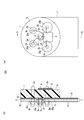
- FIG. 1A is a front view
- FIG. 1B is a sectional view taken along the line AA
- FIG. 1C is a side view of the optical module according to the first embodiment. It is an example of a shape of a projection part (a), (b).
- FIG. 8A is a front view of an optical module according to a second embodiment, and FIG. It is sectional drawing when the optical module of 2nd Embodiment is mounted in a motherboard.
- FIG. 14A is a front view of an optical module according to a third embodiment, and FIG. It is sectional drawing when the optical module of 3rd Embodiment is mounted in a motherboard. It is the (a) front view of the optical module of a 4th embodiment, the (b) DD sectional view.
- FIG. 8A is a front view of an optical module according to a second embodiment
- FIG. It is sectional drawing when the optical module of 2nd Embodiment is mounted in a motherboard.
- FIG. 14A is a front view of an
- FIG. 18A is a front view of an optical module according to a fifth embodiment
- FIG. FIG. 24A is a front view of an optical module according to a sixth embodiment
- FIG. It is (a) front view of the optical module of a comparative example
- the optical module 200 of the comparative example shown in FIGS. 10 (a) and 10 (b) is an optical module using a conventional TO-CAN type package for light reception.
- the optical module 200 includes a stem 1, five lead pins 2a to 2e, glasses 3a to 3d, a photodiode 4, an amplifier 5, and a welding portion 6. And a flexible printed circuit (FPC) 7.
- FPC flexible printed circuit
- the stem 1 is a disk-like body that supports elements such as the photodiode 4 and the amplifier 5.
- the stem 1 has a front main surface 1a (first main surface) and a back main surface 1b (second main surface).
- the stem 1 also has through holes 20a to 20d extending in the thickness direction.
- the first lead pin 2a is a pin (signal pin) for signal output.
- the second lead pin 2b is a pin (signal pin) for inverted signal output.
- the third lead pin 2 c is a bias pin of the amplifier 5.
- the fourth lead pin 2 d is a pin for biasing the photodiode 4.
- the lead pins 2a to 2d respectively penetrate through the through holes 20a to 20d of the stem 1 and are fixed by the glasses 3a to 3d.
- the fifth lead pin 2e is a ground pin for grounding.
- the fifth lead pin 2 e is directly fixed to the back major surface 1 b of the stem 1 by welding, and has the same potential as (the housing of) the stem 1.
- the weld portion 6 is a bead in which the fifth lead pin 2 e is welded to the back major surface 1 b of the stem 1.
- the diameter of the welding portion 6 is one size larger than the diameter of the fifth lead pin 2e.
- the glasses 3a to 3d are filled in each of the through holes 20a to 20d.
- the glass 3a to 3d is an insulating material filling the space between the stem 1 and each of the lead pins 2a to 2d, and electrically insulates the stem 1 (the case thereof) from each of the lead pins 2a to 2d.
- the photodiode 4 is an optical element that receives an optical signal and converts it into an electrical signal.
- the photodiode 4 is disposed on the front main surface 1 a of the stem 1 and at the center of the stem 1.
- the amplifier 5 is an electrical element that amplifies an electrical signal converted from an optical signal.
- the amplifier 5 is disposed on the front main surface 1 a of the stem 1 and near the center of the stem 1.
- the output terminal of the photodiode 4 is wire connected to the input terminal of the amplifier 5.
- the bias terminal of the photodiode 4 is wire connected to the fourth lead pin 2d.
- the bias terminal of the amplifier 5 is wire connected to the third lead pin 2c.
- the signal output terminal of the amplifier 5 is wire connected to the first lead pin 2a.
- the inverted signal output terminal of the amplifier 5 is wire connected to the second lead pin 2b.
- the FPC 7 is a bendable high-speed wiring board, and is in close contact with the back major surface 1 b of the stem 1.
- the FPC 7 includes a differential wiring for high-speed signal, which is configured of a transmission line for signals and a ground formed along the transmission lines.
- the FPC 7 also includes power supply lines for bias supply of the photodiode 4 and the amplifier 5.
- the FPC 7 can have a configuration in which, for example, a dielectric 10 (example: polyimide) having a thickness of about 50 ⁇ m is sandwiched between the upper layer wiring 12 and the lower layer ground 11. According to the FPC 7 having such a configuration, a microstrip line can be formed as a transmission line for signals, and a flexible, easy-to-handle high-speed wiring board can be obtained.
- the FPC 7 has a protective layer 19.
- the protective layer 19 protects the lower layer ground 11 from the side on which the stem 1 is provided except for the region where the lead pins 2a to 2e pass.
- the FPC 7 has a protective layer (not shown) having the same function as the protective layer 19 on the surface opposite to the surface on which the stem 1 is provided.
- the protective layer protects the upper layer wire 12 from the side opposite to the side on which the stem 1 is provided except for the area of the land (see the lands 40a to 40e in FIG. 11).
- the FPC 7 has a reinforcing plate (not shown) for suppressing bending and warping to facilitate solder mounting with respect to the portion of the protective layer 19 in contact with the stem 1.
- This reinforcing plate can be appropriately provided at any place where suppression of bending and curving works except at a place where the FPC 7 is desired to be bent, may be provided between the protective layer 19 and the lower layer ground 11, or the stem 1 and protection It may be provided between the layer 19.
- Reference numerals 40b, 40c and 40e shown in FIG. 10 (b) denote lands of the solders 8b, 8c and 8e, respectively, which serve as means for electrically connecting to the lead pins 2b, 2c and 2e.
- the FPC 7 includes five through holes 13a to 13e corresponding to the lead pins 2a to 2e. Further, the FPC 7 is provided with lands 40a to 40e around each of the through holes 13a to 13e. Electrical connection is made by inserting each of lead pins 2a to 2e into each of through holes 13a to 13e and soldering each of lead pins 2a to 2e to each of lands 40a to 40e.
- the optical module 200 can be attached to the mother board 17 by bending the FPC 7 at the end of the stem 1 so that the optical axis 16 of the light guiding means 15 is parallel to the mother board 17. . In this way, it is general to minimize the mounting space on the mother board 17 (low profile mounting).
- the optical waveguide means (optical connection component) 15 may be constituted by, for example, an optical fiber and a sleeve (receptacle) for holding the same, or one or two condenser lenses may be fixed to a hollow pipe. You may configure.
- the area of the disc of the stem 1 is roughly determined by the required number of pins and the size of the mounted element. For this reason, in the optical module 200 of the comparative example, it is difficult to make the diameter of the stem 1 smaller than a predetermined size (for example, 4 mm).
- the fifth lead pin 2 e to be a ground pin is welded to the stem 1
- a wide weld 6 is formed at the root of the fifth lead pin 2 e.
- the welded portion 6 prevents the adhesion between the stem 1 and the FPC 7, and the FPC 7 must be separated from the stem 1 by the thickness of the welded portion 6.
- the return loss is deteriorated and the inductance of the first lead pin 2a and the second lead pin 2b as signal pins is increased, thereby deteriorating the high frequency characteristics and impeding the speeding up of the transmission speed.
- the heat radiation of the optical module 200 is mainly due to the ground pin welded to the stem 1.
- the structure of the comparative example in which the heat radiation largely depends on the ground pin with a small diameter of about ⁇ ⁇ 0.4 achieves sufficient heat radiation performance. Can not.
- the reliability of the optical module itself is reduced, and the miniaturization of the optical module is hindered.
- optical module of the present invention which solves the above problems will be described with reference to a plurality of embodiments.
- the same reference numerals are used for the same members as the members described in the comparative example or in the other embodiments. Further, descriptions overlapping with the descriptions of the comparative example and the other embodiments (including the descriptions of the specific matters of the invention and the descriptions of the effects) will be omitted as appropriate, and the differences will be mainly described.
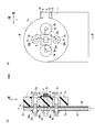
- the optical module 100A shown in FIGS. 1 (a) to 1 (c) is an optical module using the light receiving TO-CAN type package of this embodiment.
- the optical module 100A includes a stem 1, four lead pins 2a to 2d, glasses 3a to 3d, a photodiode 4 (element: optical element), and an amplifier 5 (element: electric element) and FPC 7 (substrate: flexible substrate).
- the photodiode 4 and the amplifier 5 are arranged close to each other.
- the differences between the optical module 100A of the present embodiment and the optical module 200 of the comparative example are mainly (1) not having a lead pin 2e as a ground pin of the optical module 200, (2) stem 1 (3) are provided with the lands 18 for ground connection in the FPC 7 and are soldered to the lands 18 for ground connection to provide ground connection.
- the FPC 7 has a strip shape extending in one direction, as in the optical module 200 of the comparative example. As shown in FIGS. 1A to 1C, the back major surface 1b of the stem 1 is in contact (for example, in close contact) with a partial region of the surface of the FPC. Further, the FPC 7 has a portion facing the protrusion 9 of the stem 1.
- the ground connection land 18 is a land that constitutes a ground.
- the ground connection land 18 is formed at a position facing the protrusion 9 in the FPC 7.
- the ground connection land 18 can be realized, for example, by notching the protective layer 19 or the reinforcing plate (not shown) at the formation location of the ground connection land 18 and exposing the lower layer ground 11.
- the ground connection lands 18 can also be realized, for example, by providing through holes in the protective layer 19 and the reinforcing plate (not shown).
- the solder 8 realizes the ground connection with the stem 1 at the location where the ground connection land 18 is formed.
- the protrusion 9 is disposed on the side of the stem 1.
- the protrusion 9 can be formed integrally with the disc of the stem 1 by, for example, pressing.
- the solder 8 serving as an electrical connection means with the ground connection land 18 is attached to the projection 9.
- the projection part 9 of this embodiment has the thickness similar to the plate
- the protrusions 9 can be of various shapes.
- the protrusion 9 can be formed in a rectangular shape (square pole shape).
- the ground connection land 18 is disposed on the right side of the stem 1 on the paper surface of FIG.
- the ground connection lands 18 may be disposed at any one of the circumferential positions of the stem 1 and outside (for example, the outer edge) of the stem 1. Placing the outer edge or the like outside the stem 1 provides an advantage of facilitating soldering with the stem 1.
- Such ground connection lands 18 can eliminate the need for the fifth lead pin 2e as a ground pin. Therefore, the area
- the welding portion 6 (FIG. 10) existing at the root of the ground pin is not necessary because the ground pin is not required. Therefore, the FPC 7 can be in close contact with the back main surface 1 b of the stem 1 even in the region where the weld portion 6 exists. As a result, the high frequency characteristics can be improved through the reduction of the inductance of the first lead pin 2a and the second lead pin 2b as signal pins, and the transmission speed can be increased.
- the FPC 7 is drawn out of the stem 1 from the line segment connecting the center of the stem 1 and the center of the ground connection land 18 (line segment in the left and right direction in FIG. 1). (See the arrow in FIG. 1. Hereinafter, it may be called “longitudinal direction”).
- the ground connection lands 18 project in the vertical direction in FIG. 12 (from the main body of the stem 1 to the mother board 17 side).
- the vertical dimension of the light module 100A can be reduced (low profile mounting on the motherboard 17).
- the direction orthogonal to the vertical direction may be called “horizontal direction.”
- the vertical and horizontal arrows shown in FIG. 1 are appropriately drawn in the other drawings.
- the heat dissipation of the stem 1 can be improved in the optical module 100A of the present embodiment. This is because the ground connection area between the stem 1 and the FPC 7 can be significantly increased as compared with the comparative example using the fifth lead pin 2e having a small diameter as the ground pin. Therefore, it is easy to cope with the increase in heat generation density due to the miniaturization, and as a result, the reliability of the miniaturized optical module can be improved.
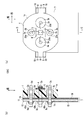
- the optical module 100B shown in FIGS. 3A and 3B is an optical module using the light receiving TO-CAN type package of the present embodiment.
- the difference between the optical module 100B of the present embodiment and the optical module 100A of the first embodiment is mainly that (1) the photodiode 4 is disposed on the amplifier 5, (2) the lead pins 2a to 2d There are two points of changing the position so as to surround the amplifier 5.
- the direction of a straight line connecting the center of the stem 1 and the center of the ground connection land 18 (or the projection 9) is lateral.
- the photodiode 4 and the amplifier 5 are disposed at the center of the main surface 1 a of the stem 1.
- the first lead pin 2a for signal and the second lead pin 2b are arranged laterally separated to such an extent that the amplifier 5 can be mounted.
- the third lead pin 2c for biasing and the fourth lead pin 2d are disposed apart in the vertical direction to such an extent that the amplifier 5 can be mounted.
- the lead pins 2a to 2d can be disposed around the amplifier 5 regardless of the position of the stem 1 in the circumferential direction. By arranging the lead pins 2a to 2d in this manner, the diameter of the stem 1 can be minimized.
- the bending position when bending the FPC 7 can be made closer to the center of the stem 1. Therefore, as shown in FIG. 4, the position which becomes the radial direction outer side vicinity of the 3rd lead pin 2c can be made into the bending position of FPC7 (refer code
- the entire optical module 100B can be miniaturized, specifically, reduced in height in the longitudinal direction.
- the protrusion part 9 is arrange
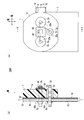
- the optical module 100C shown in FIGS. 5A and 5B is an optical module using the light receiving TO-CAN type package of the present embodiment.
- the difference between the optical module 100C of the present embodiment and the optical module 100B of the second embodiment is mainly that a flat portion is provided on the outer peripheral portion of the stem 1.
- the optical module 100C also has two ground connection lands 18 and two protrusions 9 with the center of the stem 1 interposed therebetween, and the solder 8 is provided to each of the ground connection lands 18 as well.
- the optical modules 100A and 100B are different.
- the number of ground connection lands 18 and the number of protrusions 9 in the optical module 100C, the position of the ground connection land 18 in the circumferential direction of the stem 1, and the position of the protrusions 9 are not limited to those in this embodiment. It can apply also to an embodiment.
- variety of the horizontal direction of FPC7 can be made the same as the width of the horizontal direction of the stem 1 except the part in which the land 18 for ground connection exists. Such a shape is not limited to this embodiment, and can be applied to other embodiments.
- the third lead pin 2c for biasing and the fourth lead pin 2d are vertically spaced to an extent that the amplifier 5 can be mounted. Therefore, considerable space is formed at both ends in the longitudinal direction of the stem 1. If no other element or lead pin is disposed in this empty space, the stem 1 can be further miniaturized by forming both ends in the longitudinal direction of the stem 1 flat. In other words, the shape of the stem 1 is cut out parallel to the straight line connecting the first lead pin 2a and the second lead pin 2b for signals arranged in the lateral direction across the amplifier 5, The connection lands 18, 18 and the projections 9, 9 are disposed substantially on the straight line. Such an arrangement can further miniaturize the optical module.
- the characteristic impedances of the first lead pin 2 a and the second lead pin 2 b as signal pins are preferably set to an impedance (eg, 50 ⁇ ) that matches the output impedance of the amplifier 5.
- an impedance eg, 50 ⁇
- the glasses 3c and 3d which insulate the third lead pin 2c and the fourth lead pin 2d for bias have a diameter larger than the glasses 3a and 3b which insulate the first lead pin 2a and the second lead pin 2b for signal. The dimension of the direction can be reduced.
- the first lead pin 2a and the second lead pin 2b for signal are arranged in the lateral direction with the amplifier 5 interposed therebetween, and the third lead pin for bias is provided.
- 2c and the fourth lead pin 2d are arranged in the vertical direction with the amplifier 5 interposed therebetween.
- the bending position when bending FPC7 can be closely approached to the center of the stem 1 as the notch area of the longitudinal direction both ends of the stem 1 is large. Therefore, as shown in FIG. 6, the position which becomes the radial direction outer side vicinity of the 3rd lead pin 2c can be made into the bending position of FPC7 (refer code
- the bending position indicated by reference numeral C1 is closer to the center of the stem 1 than the bending position (see reference numeral B1 in FIG. 4) shown in the second embodiment.
- the ground connection area between the stem 1 and the FPC 7 can be increased, so that the heat dissipation of the stem 1 can be further improved.
- the shape of the ground connection land 18 may be any shape as long as it can be soldered to the projection 9 of the stem 1.
- the shape is not limited to a rectangular shape (square shape), and can be various shapes such as a triangular shape (triangular shape) of the shape of the protrusion 9 illustrated in FIG.
- the optical module 100D shown in FIGS. 7A and 7B is an optical module using the TO-CAN type package for optical transmission of the present embodiment.
- the differences between the optical module 100D of this embodiment and the optical module 100A of the first embodiment are mainly (1) VCSEL (Vertical Cavity Surface Emitting Laser) 30 (a laser diode instead of the photodiode 4).
- Driver 50 Drive circuit: Element: Electric element
- Lead pin for bias One lead pin 2c And the lead pin 2a for signal input and the lead pin 2b for inverting signal input, which are three points in total.
- the VCSEL 30 resonates light in a direction perpendicular to the main surface of the stem 1 and emits an optical signal in the vertical direction.
- the driver 50 outputs a drive signal for the VCSEL 30 to emit an optical signal.
- the signal input terminal of the driver 50 is wire connected to the lead pin 2a so that an external differential signal is input, and the inverted signal input terminal of the driver 50 is wire connected to the lead pin 2b . Further, the output terminal of the driver 50 and the terminal (anode / cathode) of the VCSEL 30 are connected by wire. Thus, the drive signal is transmitted to emit an optical signal. Also, by attaching a cap (not shown) having a window or lens for light emission to the optical module 100D, transmission of an optical signal is realized.
- optical module 100A functioning as an optical reception system described in the first embodiment is also applied to an optical module 100D functioning as an optical transmission system, which is described in this embodiment. That is, even in the optical transmission system, the entire optical module can be miniaturized.
- the optical module 100E shown in FIGS. 8A and 8B is an optical module using the TO-CAN type package for optical transmission of the present embodiment.
- the difference between the optical module 100E of this embodiment and the optical module 100D of the fourth embodiment is mainly that (1) the VCSEL 30 is disposed on the driver 50, and (2) the lead pins 2a to 2c are 50, and (3) providing a flat portion on the outer peripheral portion of the stem 1 at three points.
- the VCSEL 30 and the driver 50 are disposed at the center of the front major surface 1 a of the stem 1.
- the signal first lead pins 2a and the second lead pins 2b are laterally spaced to the extent that the driver 50 can be mounted.
- one third lead pin 2c for bias is disposed below the driver 50 on the paper surface of FIG. 8A.
- the lead pins 2a to 2c are disposed close to the driver.
- the first lead pin 2a and the second lead pin 2b for signal are arranged in the lateral direction with the driver 50 interposed therebetween.
- the third lead pin 2c for bias is disposed below the driver 50 on the paper surface of FIG. 8A. That is, the dimension in the longitudinal direction of the stem 1 can be significantly reduced by cutting the stem 1 in parallel with the straight line connecting the first lead pin 2a for signal and the second lead pin 2b.
- the height of the optical module 100E can be greatly reduced by making the upper portion of FIG. 8A notched so that the shape of the FPC 7 also conforms to the shape of the stem 1.
- the optical module 100E of the fifth embodiment is substantially the same as the optical module 100D of the fourth embodiment for explaining an optical transmission system, in which the features of the first to third embodiments for explaining an optical reception system are introduced. equal. Therefore, the optical module 100E as an optical transmission system can achieve the effects of the first to third embodiments as a whole, and realize downsizing of the optical module 100E, in particular, reduction in height in the vertical direction.
- the optical module 100F shown in FIGS. 9A and 9B is an optical module using the TO-CAN type package for optical transmission of the present embodiment.
- the difference between the optical module 100F of the present embodiment and the optical module 100E of the fifth embodiment is mainly that a monitoring photodiode 21 (element: optical element) is provided instead of the driver 50.
- the VCSEL 30 and the monitoring photodiode 21 are disposed at the center of the front main surface 1 a of the stem 1.
- the VCSEL 30 is disposed on the monitor photodiode 21.
- the driver is mounted on a motherboard to which the FPC 7 is connected (not shown).
- the monitor photodiode 21 receives a light reflection signal from a cap (not shown) attached to the optical module 100 F, and generates a current according to the light transmission power from the VCSEL 30. This current is transmitted to the motherboard through the FPC 7 and used for APC (Auto Power Control) of the VCSEL 30 or the like, so that the optical transmission signal can be stabilized.
- APC Auto Power Control
- the optical module 100F of the sixth embodiment constitutes an optical transmission system different from the optical module 100E of the fifth embodiment, and includes a third lead pin 2c for biasing and a fourth lead pin 2d, A total of four lead pins 2a to 2d are provided.
- Each of the first lead pin 2a and the second lead pin 2b is for signal input and inverted signal input for the VCSEL 30, and is wire-connected to the anode and the cathode of the VCSEL 30, respectively.
- the third lead pin 2c and the fourth lead pin 2d are respectively connected to the anode and the cathode of the monitoring photodiode 21 by wire.
- the VCSEL 30 emits an optical signal in the vertical direction.
- the third lead pin 2c for biasing and the fourth lead pin 2d are spaced apart in the vertical direction to such an extent that the monitor photodiode 21 can be mounted.
- the optical module 100F according to the sixth embodiment constitutes an optical transmission system different from the optical module 100E according to the fifth embodiment, but the effects of the fifth embodiment can be achieved. That is, the optical module 100F of the sixth embodiment as an optical transmission system achieves the effects of the first to third embodiments through one step, and achieves miniaturization of the optical module 100E, in particular, reduction in height in the vertical direction. Do.
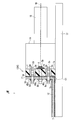
- An optical module 100G shown in FIG. 13 is an optical module using the TO-CAN type package for light reception of the present embodiment.
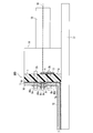
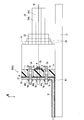
- the difference between the optical module 100G of the present embodiment and the optical module 100B of the second embodiment is that a cap 14 having a window or lens for light incidence is attached to the stem 1, and an optical connection component 15 (FIG. 4)
- a part called an optical fiber stub 24 is used, and this is centered on the cap 14 and fixed.
- the optical fiber stub 24 is a component composed of an optical fiber strand 24a and a cylindrical ceramic 24b.
- the optical fiber stub 24 has a hole of approximately the same diameter as the optical fiber strand 24a in the center of the cylindrical ceramic 24b excellent in mechanical strength, and the optical fiber strand 24a penetrates through the hole. It can be made the part which optically polished both ends later.
- YAG Yittrium Aluminum Garnet
- a component in which a cylindrical metal flange 22 (centering fixing portion) is fixed in advance to the optical fiber stub 24 and integrated is held on an XY two-axis stage (not shown).
- the metal flange 22 is a member for aligning and fixing the optical fiber stub 24 to the cap 14.
- the XY two-axis stage is a jig for aligning and fixing the optical fiber stub 24 to the cap 14 by the metal flange 22 in the longitudinal direction (X) and the lateral direction (Y).
- Peak alignment of emitted light from the cap 14 is performed in a horizontal plane (X-Y plane) using an XY two-axis stage, and the metal flange 22 and the cap 14 are fixed by YAG laser welding at the peak position. .
- an epoxy adhesive may be used, or the metal flange 22 may be crimped.
- a cylindrical metal part called Z-sleeve 23 (centering fixed part) is additionally arranged on the outer peripheral side of the metal flange 22.
- Z is a direction perpendicular to the XY plane, which is the same as the direction of the optical axis 16.
- the Z-sleeve 23 is a member fixed to the metal flange 22 to align and fix the optical fiber stub 24 to the cap 14.
- an epoxy adhesive may be used, or the Z-sleeve 23 may be crimped.
- the XY-Z 3-axis alignment can be realized by holding the optical fiber stub 24 on the XY-Z 3-axis stage (not shown).
- the XY 3 axis stage adjusts the optical fiber stub 24 to the cap 14 by the metal flange 22 and the Z-sleeve 23 in the longitudinal direction (X), the lateral direction (Y) and the vertical direction (Z). It is a jig to fix the heart.
- the X-Y-Z 3-axis stage is used to perform peak alignment of the light emitted from the cap 14, and the metal flange 22 and the cap 14 are fixed by YAG laser welding at the peak position.
- the Z stage is a jig for centering and fixing the optical fiber stub 24 to the cap 14 with respect to the direction (Z) of the optical axis 16. Therefore, the optical signal input from the optical fiber stub 24 is received at an extremely high optical coupling ratio by the photodiode 4 through which the optical axis 16 of the optical fiber stub 24 passes.
- the FPC 7 includes pads (not shown) for connection to the motherboard 17, and can transmit and receive electrical signals to and from the motherboard 17.
- the optical IF (Interface) of the optical module 100G of the present embodiment is the optical fiber stub 24, it is necessary to provide a receptacle in a device on the other side or the like.
- the configuration of the optical module 100G of the present embodiment is the reverse of the configuration of the optical module disclosed in Patent Document 1.
- the optical module 100G of the present embodiment since the optical module 100G itself is not provided with a receptacle, downsizing and a reduction in height of the optical module 100G can be realized. As a result, the optical module 100G of the present embodiment can be miniaturized to the size of the receptacle or less.
- the device on the other side where the optical module 100G is optically connected needs to be equipped with a receptacle, but the device on the other side consisting of only passive components has a large degree of freedom in design, and overall size reduction And it is easy to achieve a reduction in height. In an array configuration using a plurality of optical modules 100G, the effect of miniaturization is more remarkable.
- the present invention is not limited to the above embodiments, and modifications can be made without departing from the spirit of the present invention, and there are, for example, the following (a) to (i).
- the laser diode used in the present embodiment is not limited to the VCSEL 30, and may be a DFB (Distributed Feed Back) laser or another laser diode. Also, it may be a light emitting diode.
- the stem 1 is not limited to a discoid body, and may be a rectangular body, an oval body or the like. Further, the stem 1 may have a shape having an arc portion. In addition, the portion of the arc may have a shape which is cut out in parallel with a straight line connecting the first lead pin 2a and the second lead pin 2b.
- the electrical connection means between the ground connection land 18 and the projection 9 of the stem 1 is not limited to solder, and may be a conductive resin or the like.
- the third lead pin 2c is disposed close to the lower side of the driver 50 on the sheet of FIG. 8 (a), so that on the sheet of FIG. 8 (a), A considerably large empty space is formed above the driver 50. Therefore, the dimension of the longitudinal direction of the stem 1 can be significantly reduced by making the shape of the stem 1 a shape in which most of the empty space is cut away.
- the third lead pin 2c is disposed below the driver 50. However, the third lead pin 2c may be disposed above the driver 50. As a result, a considerably large empty space is formed below the driver 50.
- the dimension of the longitudinal direction of the stem 1 can be significantly reduced by making the shape of the stem 1 a shape in which most of the empty space is cut away. Furthermore, when the FPC 7 to which the stem 1 is in close contact is bent and mounted on the mother board 17, the bent position of the FPC 7 can be made closer to the center of the stem 1. As a result, the entire optical module 100E can be miniaturized, specifically, reduced in height in the longitudinal direction.
- the integrated component constituted by the optical fiber strand 24a and the cylindrical ceramic 24b is applied as the optical fiber stub 24, but the shape of the cylindrical ceramic 24b is The shape is not limited to a cylinder, and may be square or other shape. Also, the material is not limited to ceramic, and may be metal or plastic. Further, the miniaturization of the optical module 100G described in the seventh embodiment may be performed independently of the miniaturization by designing the diameter of the stem 1 small as described in the first to sixth embodiments. it can. Therefore, the miniaturization of the seventh embodiment and the miniaturization of the first to sixth embodiments can be combined.
- the ground connection land 18 is formed such that the direction of the line connecting the center of the stem 1 and the center of the ground connection land 18 is orthogonal to the direction in which the FPC 7 is drawn from the stem 1. Placed.
- the position of the ground connection land 18 is not limited to this.
- the ground connection land 18 may be disposed at any position within the range not exceeding both ends of the stem 1 in the longitudinal direction. Even in such an arrangement, the ground connection lands 18 do not protrude from the main body of the stem 1 toward the mother board 17, so that low height mounting on the mother board 17 is possible.
- the projection 9 is provided as a connecting portion for connecting the stem 1 and the ground connection land 18, but as in the modification (a), the stem 1 and the ground connection as a connecting portion
- the lands 18 may be directly connected to each other.
- the ground connection land 18 may be provided around the connection portion, and is not limited to the outer edge or the outer side of the stem 1.
- 100A to 100G optical module 1 stem 1a front main surface (first main surface) 1b back main surface (second main surface) 2a, 2b lead pins (signal pins) 2c, 2d lead pin (pin for bias) 2e Lead pin (ground pin for grounding) 3a to 3d glass (insulation material) 4 Photodiode (element: optical element) 5 Amplifier (element: electric element) 7 FPC (board: flexible board) 8, 8a to 8d solder 9 protrusion 10 dielectric 10 lower layer ground 12 upper layer wiring 14 cap 15 optical waveguide means (optical connection parts) Reference Signs List 16 optical axis 17 mother board 18 ground connection land 19 protective layer 20a to 20d through hole 21 monitor photodiode (element: optical element) 22 (for YAG welding) metal flange (centering fixed part) 23 Z-Sleeve (alignment part) 24 optical fiber stub 24a optical fiber strand 24b cylindrical ceramic 30 VCSEL (laser diode: element: optical element) 40a to
Landscapes
- Physics & Mathematics (AREA)
- General Physics & Mathematics (AREA)
- Optics & Photonics (AREA)
- Light Receiving Elements (AREA)
- Semiconductor Lasers (AREA)
- Optical Couplings Of Light Guides (AREA)
Abstract
Description
ステムと、
前記ステムを貫通するリードピンと、
前記ステムと前記リードピンとの間を埋める絶縁材と、
前記ステムの第1の主面に配置されており、前記リードピンに接続している素子と、
前記ステムの第2の主面に接している基板と、
前記ステムに装着するキャップと、
光ファイバスタブと、
前記光ファイバスタブを前記キャップに調心固定させる調心固定部と、を備える、
ことを特徴とする光モジュールである。
その他の発明については、実施形態で説明する。
まず、本発明の比較例となる光モジュールについて説明する。図10(a),(b)に示す比較例の光モジュール200は、従来の光受信用TO-CAN型パッケージを用いる光モジュールである。図10(a),(b)に示すように、光モジュール200は、ステム1と、5本のリードピン2a~2eと、ガラス3a~3dと、フォトダイオード4と、増幅器5と、溶接部6と、FPC(Flexible Printed Circuit:フレキシブル基板)7と、を備える。
溶接部6は、第5のリードピン2eをステム1の裏主面1bに溶接されるビードである。溶接部6の径は、第5のリードピン2eの径よりも一回り大きい。
増幅器5は、光信号から変換された電気信号を増幅する電気素子である。増幅器5は、ステム1の表主面1aに、かつ、ステム1の中心付近に配置されている。
上記のように構成することで、フォトダイオード4が受信した光信号が第1のリードピン2aと第2のリードピン2bとの差動電気信号として出力される。この出力された差動電気信号は、光受信用TO-CAN型パッケージに取り付けられたFPC7を介して外部に取り出される。
図10(b)に示す符号40b,40c,40eはそれぞれ、リードピン2b,2c,2eの各々との電気的な接続手段となるはんだ8b,8c,8eの各々のランドである。
図1(a)~(c)に示す光モジュール100Aは、本実施形態の光受信用TO-CAN型パッケージを用いる光モジュールである。図1(a)~(c)に示すように、光モジュール100Aは、ステム1と、4本のリードピン2a~2dと、ガラス3a~3dと、フォトダイオード4(素子:光素子)と、増幅器5(素子:電気素子)と、FPC7(基板:フレキシブル基板)と、を備える。フォトダイオード4および増幅器5は、互いに近傍に配置されている。
なお、本実施形態の突起部9は、ステム1の板厚と同様の厚みを有しているが、これに限定されない。
なお、図1に示すように、縦方向に直交する方向を「横方向」と呼ぶ場合がある。図1に示す縦方向および横方向の矢印は、他の図にも適宜描かれている。
図3(a)、(b)に示す光モジュール100Bは、本実施形態の光受信用TO-CAN型パッケージを用いる光モジュールである。本実施形態の光モジュール100Bと、第1の実施形態の光モジュール100Aとの相違点は、主に、(1)フォトダイオード4を増幅器5上に配置したこと、(2)リードピン2a~2dを増幅器5を囲うような位置に変更していること、の2点である。ステム1の中心とグランド接続用ランド18(または突起部9)の中心とを結ぶ直線の方向は、横方向である。
また、突起部9は、ステム1の側面に配置されているので、FPC7を組み付ける際の目印となる。よって、光モジュール100Aの製造者は、突起部9を参照することで、ピン配置が図3のように中心対称になっている場合においても、ステム1とFPC7の端子を間違えなく接続することが容易になる。
図5(a)、(b)に示す光モジュール100Cは、本実施形態の光受信用TO-CAN型パッケージを用いる光モジュールである。本実施形態の光モジュール100Cと、第2の実施形態の光モジュール100Bとの相違点は、主に、ステム1の外周部に平坦部を設けたことである。また、光モジュール100Cは、ステム1の中心を挟んで2つのグランド接続用ランド18と、2つの突起部9とを備え、グランド接続用ランド18の各々にはんだ8が設けられている点においても光モジュール100A,100Bとは相違している。なお、光モジュール100Cにおけるグランド接続用ランド18の個数、突起部9の個数、ステム1の周方向におけるグランド接続用ランド18の位置、突起部9の位置は、本実施形態に限らず、他の実施形態にも適用することができる。また、図5(a)に示すように、FPC7の横方向の幅は、グランド接続用ランド18が存在する部分を除いて、ステム1の横方向の幅と同じにすることができる。このような形状も本実施形態に限らず、他の実施の形態にも適用できる。
図7(a)、(b)に示す光モジュール100Dは、本実施形態の光送信用TO-CAN型パッケージを用いる光モジュールである。本実施形態の光モジュール100Dと、第1の実施形態の光モジュール100Aとの相違点は、主に、(1)フォトダイオード4の代わりにレーザダイオードであるVCSEL(Vertical Cavity Surface Emitting LASER)30(レーザダイオード:素子:光素子)を備えたこと、(2)増幅器5の代わりにドライバ50(駆動回路:素子:電気素子)を備えたこと、(3)バイアス用のリードピンを1本のリードピン2cにし、信号入力用のリードピン2aと、反転信号入力用のリードピン2bの計3本のリードピンを備えたこと、の3点である。
ドライバ50は、VCSEL30が光信号を出射するための駆動信号を出力する。
図8(a)、(b)に示す光モジュール100Eは、本実施形態の光送信用TO-CAN型パッケージを用いる光モジュールである。本実施形態の光モジュール100Eと、第4の実施形態の光モジュール100Dとの相違点は、主に、(1)VCSEL30をドライバ50の上に配置したこと、(2)リードピン2a~2cをドライバ50を囲うような位置に変更していること、(3)ステム1の外周部に平坦部を設けたこと、の3点である。図8(a)に示すように、VCSEL30およびドライバ50は、ステム1の表主面1aの中心に配置されている。
図9(a)、(b)に示す光モジュール100Fは、本実施形態の光送信用TO-CAN型パッケージを用いる光モジュールである。本実施形態の光モジュール100Fと、第5の実施形態の光モジュール100Eとの相違点は、主に、ドライバ50の代わりにモニタ用フォトダイオード21(素子:光素子)を備えることである。図8(a)に示すように、VCSEL30およびモニタ用フォトダイオード21は、ステム1の表主面1aの中心に配置されている。また、VCSEL30は、モニタ用フォトダイオード21の上に配置されている。なお、ドライバはFPC7が接続されるマザーボードに搭載される(図示せず)。
図13に示す光モジュール100Gは、本実施形態の光受信用TO-CAN型パッケージを用いる光モジュールである。本実施形態の光モジュール100Gと、第2の実施形態の光モジュール100Bとの相違点は、光入射用の窓またはレンズを備えるキャップ14をステム1に装着し、さらに光接続部品15(図4参照)として光ファイバスタブ24と呼ばれる部品を用い、これをキャップ14上に調心固定していることである。光ファイバスタブ24は、光ファイバ素線24aと円筒型セラミック24bから構成される部品である。好適には、光ファイバスタブ24は、機械的強度に優れる円筒型セラミック24bの中心に光ファイバ素線24aとほぼ同径の穴を開け、その穴の中に光ファイバ素線24aを貫通させた後に両端を光学研磨した部品とすることができる。
本発明は、上記実施形態に限定されることなく、本発明の趣旨を逸脱しない範囲で、変更実施が可能であり、例えば、以下の(a)~(i)がある。
(a)本実施形態では、ステム1に突起部9が備えられた場合について説明したが、突起部9を備えていない形態のステムとし、FPC7のグランド接続用ランド18とステム本体部の側面とをはんだ付け(グランド接続)しても構わない。
(b)本実施形態で用いるレーザダイオードは、VCSEL30に限定されず、DFB(Distributed FeedBack)レーザやその他のレーザダイオードであってもよい。また、発光ダイオードであっても構わない。
(c)本実施形態では、基板としてFPC7を適用した場合について説明したが、FPC7に限らず、リジッドな基板であっても本発明を適用することができる。
(e)グランド接続用ランド18とステム1の突起部9との電気的な接続手段は、はんだに限定されず、導電性樹脂などでもよい。
(g)第5の実施形態にて、第3のリードピン2cを、ドライバ50の下側に配置したが、第3のリードピン2cを、ドライバ50の上側に配置してもよい。これにより、ドライバ50の下側に相当大きな空きスペースが形成される。よって、ステム1の形状を、この空きスペースの大部分を切り欠いた形状とすることで、ステム1の縦方向の寸法を大幅に小さくすることができる。さらに、ステム1を密着させたFPC7を屈曲させてマザーボード17に実装させる際、FPC7の屈曲位置をステム1の中心により近付けることができる。その結果、光モジュール100E全体を小型化、具体的には、縦方向に関して低背化することができる。
また、グランド接続用ランド18は、接続部の周辺に設けられればよく、ステム1の外縁や外側に限定されない。
その他、本発明の構成要素の形状、材質、機能などについて、本発明の趣旨を逸脱しない範囲で適宜変更が可能である。
1 ステム
1a 表主面(第1の主面)
1b 裏主面(第2の主面)
2a,2b リードピン(信号用ピン)
2c,2d リードピン(バイアス用ピン)
2e リードピン(接地用のグランドピン)
3a~3d ガラス(絶縁材)
4 フォトダイオード(素子:光素子)
5 増幅器(素子:電気素子)
7 FPC(基板:フレキシブル基板)
8,8a~8d はんだ
9 突起部
10 誘電体
11 下層グランド
12 上層配線
14 キャップ
15 光導波手段(光接続部品)
16 光軸
17 マザーボード
18 グランド接続用ランド
19 保護層
20a~20d 貫通孔
21 モニタ用フォトダイオード(素子:光素子)
22 (YAG溶接用)金属製フランジ(調心固定部)
23 Z-スリーブ(調心固定部)
24 光ファイバスタブ
24a 光ファイバ素線
24b 円筒型セラミック
30 VCSEL(レーザダイオード:素子:光素子)
40a~40e ランド
50 ドライバ(駆動回路:素子:電気素子)
Claims (14)
- ステムと、
前記ステムを貫通するリードピンと、
前記ステムと前記リードピンとの間を埋める絶縁材と、
前記ステムの第1の主面に配置されており、前記リードピンに接続している素子と、
前記ステムの第2の主面に接している基板と、
前記ステムに装着するキャップと、
光ファイバスタブと、
前記光ファイバスタブを前記キャップに調心固定させる調心固定部と、を備える、
ことを特徴とする光モジュール。 - 前記基板は、前記ステムと直接接続されるグランド接続用ランドを備える、
ことを特徴とする請求項1に記載の光モジュール。 - 前記素子としての光素子が、前記素子としての電気素子の上に配置されている、
ことを特徴とする請求項2に記載の光モジュール。 - 前記基板が、フレキシブル基板であり、
前記ステムの中心から前記グランド接続用ランドの中心を結ぶ線分が、前記フレキシブル基板が前記ステムから引き出されている方向と略直交している、
ことを特徴とする請求項2又は請求項3に記載の光モジュール。 - 前記リードピンは、2本の信号用ピンを含んでおり、
前記2本の信号用ピンは、前記ステムの中心と前記グランド接続用ランドの中心とを結ぶ略直線上に、かつ、前記ステムの中心を対称にして配置されている、
ことを特徴とする請求項2から請求項4のいずれか1項に記載の光モジュール。 - 前記ステムは、孤の部分を有する形状であり、前記孤の部分が、前記2本の信号用ピンを結ぶ直線に略平行に切り欠かれた形状を呈している、
ことを特徴とする請求項5に記載の光モジュール。 - 前記ステムは、前記グランド接続用ランドに対向する突起部を備える、
ことを特徴とする請求項2から請求項6のいずれか1項に記載の光モジュール。 - 前記グランド接続用ランドおよび前記グランド接続用ランドに対応する前記突起部が2以上であることを特徴とする請求項7に記載の光モジュール。
- 前記素子としての光素子はフォトダイオードであり、前記素子としての電気素子は増幅器である、
ことを特徴とする請求項2から請求項8のいずれか1項に記載の光モジュール。 - 前記素子としての光素子はレーザダイオードまたは発光ダイオードであり、前記素子としての電気素子はドライバである、
ことを特徴とする請求項2から請求項8のいずれか1項に記載の光モジュール。 - 前記グランド接続用ランドが2以上であることを特徴とする請求項2から請求項10のいずれか1項に記載の光モジュール。
- 前記素子が互いに近傍に配置されていることを特徴とする請求項2から請求項11のいずれか1項に記載の光モジュール。
- 前記グランド接続用ランドは、前記ステムよりも外側で、前記ステムと直接接続される、
ことを特徴とする請求項2から請求項12のいずれか1項に記載の光モジュール。 - ステムと、
前記ステムを貫通するリードピンと、
前記ステムと前記リードピンとの間を埋める絶縁材と、
前記ステムの第1の主面に配置されており、前記リードピンに接続している素子と、
前記ステムの第2の主面に接している基板と、を備え、
前記基板は、前記ステムと直接接続されるグランド接続用ランドを備える、
ことを特徴とする光モジュール。
Priority Applications (6)
| Application Number | Priority Date | Filing Date | Title |
|---|---|---|---|
| US16/629,756 US11327258B2 (en) | 2017-07-11 | 2017-07-11 | Optical module |
| EP17917577.3A EP3667378B1 (en) | 2017-07-11 | 2017-07-11 | Optical module |
| CN201780092007.2A CN110741298B (zh) | 2017-07-11 | 2017-07-11 | 光模块 |
| JP2019529360A JP7057357B2 (ja) | 2017-07-11 | 2017-07-11 | 光モジュール |
| PCT/JP2017/025298 WO2019012607A1 (ja) | 2017-07-11 | 2017-07-11 | 光モジュール |
| TW106126369A TWI663737B (zh) | 2017-07-11 | 2017-08-04 | 光模組 |
Applications Claiming Priority (1)
| Application Number | Priority Date | Filing Date | Title |
|---|---|---|---|
| PCT/JP2017/025298 WO2019012607A1 (ja) | 2017-07-11 | 2017-07-11 | 光モジュール |
Publications (1)
| Publication Number | Publication Date |
|---|---|
| WO2019012607A1 true WO2019012607A1 (ja) | 2019-01-17 |
Family
ID=65002125
Family Applications (1)
| Application Number | Title | Priority Date | Filing Date |
|---|---|---|---|
| PCT/JP2017/025298 Ceased WO2019012607A1 (ja) | 2017-07-11 | 2017-07-11 | 光モジュール |
Country Status (6)
| Country | Link |
|---|---|
| US (1) | US11327258B2 (ja) |
| EP (1) | EP3667378B1 (ja) |
| JP (1) | JP7057357B2 (ja) |
| CN (1) | CN110741298B (ja) |
| TW (1) | TWI663737B (ja) |
| WO (1) | WO2019012607A1 (ja) |
Cited By (1)
| Publication number | Priority date | Publication date | Assignee | Title |
|---|---|---|---|---|
| JPWO2022113174A1 (ja) * | 2020-11-24 | 2022-06-02 |
Families Citing this family (5)
| Publication number | Priority date | Publication date | Assignee | Title |
|---|---|---|---|---|
| JP7454996B2 (ja) * | 2020-05-11 | 2024-03-25 | CIG Photonics Japan株式会社 | 光モジュール |
| JP7542419B2 (ja) * | 2020-12-02 | 2024-08-30 | CIG Photonics Japan株式会社 | 光モジュール |
| JP2022143754A (ja) * | 2021-03-18 | 2022-10-03 | CIG Photonics Japan株式会社 | 光モジュール |
| US12085770B2 (en) * | 2021-10-13 | 2024-09-10 | Electronics And Telecommunications Research Institute | Optical submodule |
| US20250112437A1 (en) * | 2023-09-29 | 2025-04-03 | Keysight Technologies, Inc. | Bandwidth improvement of through-hole distributed feedback laser |
Citations (11)
| Publication number | Priority date | Publication date | Assignee | Title |
|---|---|---|---|---|
| JP2001284700A (ja) * | 2000-03-31 | 2001-10-12 | Furukawa Electric Co Ltd:The | 半導体レーザモジュール |
| JP2003241029A (ja) | 2002-02-14 | 2003-08-27 | Sumitomo Electric Ind Ltd | 光モジュールおよび光送受信器 |
| JP2005294429A (ja) * | 2004-03-31 | 2005-10-20 | Murata Mfg Co Ltd | 光受信モジュール |
| JP2007123739A (ja) * | 2005-10-31 | 2007-05-17 | Sony Corp | 光送信モジュール、光送受信モジュール及び光通信装置 |
| JP2009253064A (ja) * | 2008-04-08 | 2009-10-29 | Sumitomo Electric Ind Ltd | 双方向光モジュール |
| JP2009302438A (ja) * | 2008-06-17 | 2009-12-24 | Opnext Japan Inc | 光半導体装置 |
| JP2011129546A (ja) * | 2009-12-15 | 2011-06-30 | Nippon Telegr & Teleph Corp <Ntt> | 光モジュール製造方法及び検査方法 |
| US20120207437A1 (en) * | 2011-02-10 | 2012-08-16 | Electronics And Telecommunications Research Institute | Optical module |
| JP2012256692A (ja) | 2011-06-08 | 2012-12-27 | Mitsubishi Electric Corp | 光モジュール |
| JP2016018969A (ja) * | 2014-07-11 | 2016-02-01 | 日本オクラロ株式会社 | 光モジュール、光送受信モジュール、及びフレキシブル基板 |
| JP2017108064A (ja) * | 2015-12-11 | 2017-06-15 | 日本オクラロ株式会社 | 光モジュール |
Family Cites Families (22)
| Publication number | Priority date | Publication date | Assignee | Title |
|---|---|---|---|---|
| JP2001296457A (ja) * | 1999-10-07 | 2001-10-26 | Sumitomo Electric Ind Ltd | 光送受信器 |
| US7215886B2 (en) | 2002-02-04 | 2007-05-08 | Hitachi, Ltd. | Optical communication module |
| EP1388916A1 (en) * | 2002-08-09 | 2004-02-11 | Agilent Technologies, Inc. - a Delaware corporation - | Optoelectronic package |
| JP4586337B2 (ja) * | 2002-08-26 | 2010-11-24 | 住友電気工業株式会社 | 半導体レーザモジュールおよび半導体レーザ装置 |
| JP2004349567A (ja) * | 2003-05-23 | 2004-12-09 | Kyocera Corp | 半導体素子収納用パッケージおよび半導体装置 |
| US7315698B2 (en) | 2003-10-22 | 2008-01-01 | Sumitomo Electric Industries, Ltd. | Optical module and an optical receiver using the same |
| JP2006351610A (ja) * | 2005-06-13 | 2006-12-28 | Sumitomo Electric Ind Ltd | 光モジュール |
| JP2007042756A (ja) | 2005-08-01 | 2007-02-15 | Sony Corp | 光デバイスと光通信装置 |
| US20070051877A1 (en) * | 2005-09-06 | 2007-03-08 | Fuji Xerox Co., Ltd. | Optical transmitter-receiver, optical transmitter-receiver module, and optical communication device |
| JP5076460B2 (ja) * | 2005-12-07 | 2012-11-21 | 住友電気工業株式会社 | サーミスタを搭載した光サブアセンブリ |
| US7467898B2 (en) * | 2006-03-29 | 2008-12-23 | Sumitomo Electric Industries, Ltd. | Optical transceiver installing bi-directional optical sub-assembly |
| JP2008177310A (ja) * | 2007-01-18 | 2008-07-31 | Sumitomo Electric Ind Ltd | 光モジュール及びそれを搭載した光トランシーバ |
| GB2463226B (en) * | 2008-07-22 | 2011-01-12 | Conjunct Ltd | Optical sub-assembly |
| US8145061B2 (en) * | 2009-01-13 | 2012-03-27 | Sumitomo Electric Industries, Ltd. | Optical module implementing a light-receiving device and a light-transmitting device within a common housing |
| TW201113985A (en) * | 2009-06-10 | 2011-04-16 | Coretek Opto Corp | Header structure of opto-electronic element and opto-electronic element using the same |
| TWM375895U (en) * | 2009-08-14 | 2010-03-11 | Ezconn Corp | Light source apparatus |
| US20110085767A1 (en) * | 2009-10-09 | 2011-04-14 | Emcore Corporation | Cooled Laser Module |
| US8721193B2 (en) * | 2010-08-13 | 2014-05-13 | Finisar Corporation | Electronic module having multiple flex circuit connectors |
| US8913388B2 (en) * | 2012-01-18 | 2014-12-16 | Finisar Corporation | Thermally conductive flexible member for heat transfer |
| JP5958364B2 (ja) * | 2013-01-28 | 2016-07-27 | 日立金属株式会社 | 光モジュール |
| US9063309B2 (en) * | 2013-04-22 | 2015-06-23 | Avago Technologies General Ip (Singapore) Pte. Ltd. | Optoelectronic module with flexible substrate |
| CN105610040A (zh) * | 2014-11-25 | 2016-05-25 | 青岛海信宽带多媒体技术有限公司 | 一种激光发射器 |
-
2017
- 2017-07-11 EP EP17917577.3A patent/EP3667378B1/en active Active
- 2017-07-11 US US16/629,756 patent/US11327258B2/en active Active
- 2017-07-11 WO PCT/JP2017/025298 patent/WO2019012607A1/ja not_active Ceased
- 2017-07-11 JP JP2019529360A patent/JP7057357B2/ja active Active
- 2017-07-11 CN CN201780092007.2A patent/CN110741298B/zh active Active
- 2017-08-04 TW TW106126369A patent/TWI663737B/zh active
Patent Citations (11)
| Publication number | Priority date | Publication date | Assignee | Title |
|---|---|---|---|---|
| JP2001284700A (ja) * | 2000-03-31 | 2001-10-12 | Furukawa Electric Co Ltd:The | 半導体レーザモジュール |
| JP2003241029A (ja) | 2002-02-14 | 2003-08-27 | Sumitomo Electric Ind Ltd | 光モジュールおよび光送受信器 |
| JP2005294429A (ja) * | 2004-03-31 | 2005-10-20 | Murata Mfg Co Ltd | 光受信モジュール |
| JP2007123739A (ja) * | 2005-10-31 | 2007-05-17 | Sony Corp | 光送信モジュール、光送受信モジュール及び光通信装置 |
| JP2009253064A (ja) * | 2008-04-08 | 2009-10-29 | Sumitomo Electric Ind Ltd | 双方向光モジュール |
| JP2009302438A (ja) * | 2008-06-17 | 2009-12-24 | Opnext Japan Inc | 光半導体装置 |
| JP2011129546A (ja) * | 2009-12-15 | 2011-06-30 | Nippon Telegr & Teleph Corp <Ntt> | 光モジュール製造方法及び検査方法 |
| US20120207437A1 (en) * | 2011-02-10 | 2012-08-16 | Electronics And Telecommunications Research Institute | Optical module |
| JP2012256692A (ja) | 2011-06-08 | 2012-12-27 | Mitsubishi Electric Corp | 光モジュール |
| JP2016018969A (ja) * | 2014-07-11 | 2016-02-01 | 日本オクラロ株式会社 | 光モジュール、光送受信モジュール、及びフレキシブル基板 |
| JP2017108064A (ja) * | 2015-12-11 | 2017-06-15 | 日本オクラロ株式会社 | 光モジュール |
Non-Patent Citations (1)
| Title |
|---|
| See also references of EP3667378A4 |
Cited By (3)
| Publication number | Priority date | Publication date | Assignee | Title |
|---|---|---|---|---|
| JPWO2022113174A1 (ja) * | 2020-11-24 | 2022-06-02 | ||
| JP7204065B2 (ja) | 2020-11-24 | 2023-01-13 | 三菱電機株式会社 | 光モジュール |
| CN116648835A (zh) * | 2020-11-24 | 2023-08-25 | 三菱电机株式会社 | 光模块 |
Also Published As
| Publication number | Publication date |
|---|---|
| EP3667378A1 (en) | 2020-06-17 |
| TW201909436A (zh) | 2019-03-01 |
| JPWO2019012607A1 (ja) | 2020-05-21 |
| CN110741298A (zh) | 2020-01-31 |
| US20200292764A1 (en) | 2020-09-17 |
| EP3667378B1 (en) | 2026-04-08 |
| EP3667378A4 (en) | 2020-08-26 |
| TWI663737B (zh) | 2019-06-21 |
| JP7057357B2 (ja) | 2022-04-19 |
| US11327258B2 (en) | 2022-05-10 |
| CN110741298B (zh) | 2022-11-15 |
Similar Documents
| Publication | Publication Date | Title |
|---|---|---|
| JP7057357B2 (ja) | 光モジュール | |
| US7306377B2 (en) | Integrated optical sub-assembly having epoxy chip package | |
| KR101512816B1 (ko) | 플렉시블 인쇄회로기판 및 이를 포함하는 광통신 모듈 | |
| JP5104251B2 (ja) | 光モジュール | |
| CN100514104C (zh) | 光模组及其制造方法、光通信装置、电子设备 | |
| US7127142B2 (en) | Optical communication device | |
| JP4015440B2 (ja) | 光通信モジュール | |
| JP2008040318A (ja) | 多チャンネル光モジュールの製造方法 | |
| JP5195087B2 (ja) | 光電気変換デバイス、光電気変換モジュールおよび光電気変換デバイスの製造方法 | |
| US20090148096A1 (en) | Optical interconnection device | |
| US9588313B2 (en) | Optical device package and optical device apparatus | |
| JP5093121B2 (ja) | 光モジュール | |
| JP2008015336A (ja) | 回路基板及び半導体デバイスの光結合方法 | |
| JP2008226988A (ja) | 光電変換モジュール | |
| JPWO2005057262A1 (ja) | 光モジュールおよびその製造方法 | |
| JP7087738B2 (ja) | 光通信装置、及び光通信装置の製造方法 | |
| JP2010034386A (ja) | 光半導体装置 | |
| JP6832091B2 (ja) | 光モジュール | |
| JP6589345B2 (ja) | 光配線基板、光モジュール、及び光アクティブケーブル | |
| US6973227B2 (en) | Optical communication device | |
| JP2009253176A (ja) | 光電変換モジュール及び光サブアセンブリ | |
| JP6776507B2 (ja) | 光モジュール、及び光アクティブケーブル | |
| JP6690131B2 (ja) | 光配線基板、光モジュール、及び光アクティブケーブル | |
| JP2004309925A (ja) | 光モジュール及びその製造方法、光通信装置、電子機器 | |
| JP2005222003A (ja) | マウント、光部品、光送受信モジュール及び双方向光通信モジュール |
Legal Events
| Date | Code | Title | Description |
|---|---|---|---|
| 121 | Ep: the epo has been informed by wipo that ep was designated in this application |
Ref document number: 17917577 Country of ref document: EP Kind code of ref document: A1 |
|
| ENP | Entry into the national phase |
Ref document number: 2019529360 Country of ref document: JP Kind code of ref document: A |
|
| NENP | Non-entry into the national phase |
Ref country code: DE |
|
| ENP | Entry into the national phase |
Ref document number: 2017917577 Country of ref document: EP Effective date: 20200211 |
|
| WWG | Wipo information: grant in national office |
Ref document number: 2017917577 Country of ref document: EP |