WO2019029219A1 - 一种光学结构及其控制方法、显示器件 - Google Patents
一种光学结构及其控制方法、显示器件 Download PDFInfo
- Publication number
- WO2019029219A1 WO2019029219A1 PCT/CN2018/087255 CN2018087255W WO2019029219A1 WO 2019029219 A1 WO2019029219 A1 WO 2019029219A1 CN 2018087255 W CN2018087255 W CN 2018087255W WO 2019029219 A1 WO2019029219 A1 WO 2019029219A1
- Authority
- WO
- WIPO (PCT)
- Prior art keywords
- transparent electrode
- voltage
- sub
- region
- ambient light
- Prior art date
- Legal status (The legal status is an assumption and is not a legal conclusion. Google has not performed a legal analysis and makes no representation as to the accuracy of the status listed.)
- Ceased
Links
Images


Classifications
-
- E—FIXED CONSTRUCTIONS
- E06—DOORS, WINDOWS, SHUTTERS, OR ROLLER BLINDS IN GENERAL; LADDERS
- E06B—FIXED OR MOVABLE CLOSURES FOR OPENINGS IN BUILDINGS, VEHICLES, FENCES OR LIKE ENCLOSURES IN GENERAL, e.g. DOORS, WINDOWS, BLINDS, GATES
- E06B3/00—Window sashes, door leaves, or like elements for closing wall or like openings; Layout of fixed or moving closures, e.g. windows in wall or like openings; Features of rigidly-mounted outer frames relating to the mounting of wing frames
- E06B3/66—Units comprising two or more parallel glass or like panes permanently secured together
- E06B3/67—Units comprising two or more parallel glass or like panes permanently secured together characterised by additional arrangements or devices for heat or sound insulation or for controlled passage of light
- E06B3/6715—Units comprising two or more parallel glass or like panes permanently secured together characterised by additional arrangements or devices for heat or sound insulation or for controlled passage of light specially adapted for increased thermal insulation or for controlled passage of light
- E06B3/6722—Units comprising two or more parallel glass or like panes permanently secured together characterised by additional arrangements or devices for heat or sound insulation or for controlled passage of light specially adapted for increased thermal insulation or for controlled passage of light with adjustable passage of light
-
- G—PHYSICS
- G02—OPTICS
- G02F—OPTICAL DEVICES OR ARRANGEMENTS FOR THE CONTROL OF LIGHT BY MODIFICATION OF THE OPTICAL PROPERTIES OF THE MEDIA OF THE ELEMENTS INVOLVED THEREIN; NON-LINEAR OPTICS; FREQUENCY-CHANGING OF LIGHT; OPTICAL LOGIC ELEMENTS; OPTICAL ANALOGUE/DIGITAL CONVERTERS
- G02F1/00—Devices or arrangements for the control of the intensity, colour, phase, polarisation or direction of light arriving from an independent light source, e.g. switching, gating or modulating; Non-linear optics
- G02F1/01—Devices or arrangements for the control of the intensity, colour, phase, polarisation or direction of light arriving from an independent light source, e.g. switching, gating or modulating; Non-linear optics for the control of the intensity, phase, polarisation or colour
- G02F1/13—Devices or arrangements for the control of the intensity, colour, phase, polarisation or direction of light arriving from an independent light source, e.g. switching, gating or modulating; Non-linear optics for the control of the intensity, phase, polarisation or colour based on liquid crystals, e.g. single liquid crystal display cells
- G02F1/133—Constructional arrangements; Operation of liquid crystal cells; Circuit arrangements
- G02F1/13306—Circuit arrangements or driving methods for the control of single liquid crystal cells
- G02F1/13318—Circuits comprising a photodetector
-
- G—PHYSICS
- G02—OPTICS
- G02F—OPTICAL DEVICES OR ARRANGEMENTS FOR THE CONTROL OF LIGHT BY MODIFICATION OF THE OPTICAL PROPERTIES OF THE MEDIA OF THE ELEMENTS INVOLVED THEREIN; NON-LINEAR OPTICS; FREQUENCY-CHANGING OF LIGHT; OPTICAL LOGIC ELEMENTS; OPTICAL ANALOGUE/DIGITAL CONVERTERS
- G02F1/00—Devices or arrangements for the control of the intensity, colour, phase, polarisation or direction of light arriving from an independent light source, e.g. switching, gating or modulating; Non-linear optics
- G02F1/01—Devices or arrangements for the control of the intensity, colour, phase, polarisation or direction of light arriving from an independent light source, e.g. switching, gating or modulating; Non-linear optics for the control of the intensity, phase, polarisation or colour
- G02F1/13—Devices or arrangements for the control of the intensity, colour, phase, polarisation or direction of light arriving from an independent light source, e.g. switching, gating or modulating; Non-linear optics for the control of the intensity, phase, polarisation or colour based on liquid crystals, e.g. single liquid crystal display cells
- G02F1/133—Constructional arrangements; Operation of liquid crystal cells; Circuit arrangements
- G02F1/1333—Constructional arrangements; Manufacturing methods
- G02F1/1334—Constructional arrangements; Manufacturing methods based on polymer dispersed liquid crystals, e.g. microencapsulated liquid crystals
-
- G—PHYSICS
- G02—OPTICS
- G02F—OPTICAL DEVICES OR ARRANGEMENTS FOR THE CONTROL OF LIGHT BY MODIFICATION OF THE OPTICAL PROPERTIES OF THE MEDIA OF THE ELEMENTS INVOLVED THEREIN; NON-LINEAR OPTICS; FREQUENCY-CHANGING OF LIGHT; OPTICAL LOGIC ELEMENTS; OPTICAL ANALOGUE/DIGITAL CONVERTERS
- G02F1/00—Devices or arrangements for the control of the intensity, colour, phase, polarisation or direction of light arriving from an independent light source, e.g. switching, gating or modulating; Non-linear optics
- G02F1/01—Devices or arrangements for the control of the intensity, colour, phase, polarisation or direction of light arriving from an independent light source, e.g. switching, gating or modulating; Non-linear optics for the control of the intensity, phase, polarisation or colour
- G02F1/13—Devices or arrangements for the control of the intensity, colour, phase, polarisation or direction of light arriving from an independent light source, e.g. switching, gating or modulating; Non-linear optics for the control of the intensity, phase, polarisation or colour based on liquid crystals, e.g. single liquid crystal display cells
- G02F1/133—Constructional arrangements; Operation of liquid crystal cells; Circuit arrangements
- G02F1/1333—Constructional arrangements; Manufacturing methods
- G02F1/1343—Electrodes
- G02F1/134309—Electrodes characterised by their geometrical arrangement
-
- G—PHYSICS
- G02—OPTICS
- G02F—OPTICAL DEVICES OR ARRANGEMENTS FOR THE CONTROL OF LIGHT BY MODIFICATION OF THE OPTICAL PROPERTIES OF THE MEDIA OF THE ELEMENTS INVOLVED THEREIN; NON-LINEAR OPTICS; FREQUENCY-CHANGING OF LIGHT; OPTICAL LOGIC ELEMENTS; OPTICAL ANALOGUE/DIGITAL CONVERTERS
- G02F1/00—Devices or arrangements for the control of the intensity, colour, phase, polarisation or direction of light arriving from an independent light source, e.g. switching, gating or modulating; Non-linear optics
- G02F1/01—Devices or arrangements for the control of the intensity, colour, phase, polarisation or direction of light arriving from an independent light source, e.g. switching, gating or modulating; Non-linear optics for the control of the intensity, phase, polarisation or colour
- G02F1/13—Devices or arrangements for the control of the intensity, colour, phase, polarisation or direction of light arriving from an independent light source, e.g. switching, gating or modulating; Non-linear optics for the control of the intensity, phase, polarisation or colour based on liquid crystals, e.g. single liquid crystal display cells
- G02F1/133—Constructional arrangements; Operation of liquid crystal cells; Circuit arrangements
- G02F1/135—Liquid crystal cells structurally associated with a photoconducting or a ferro-electric layer, the properties of which can be optically or electrically varied
-
- G—PHYSICS
- G02—OPTICS
- G02F—OPTICAL DEVICES OR ARRANGEMENTS FOR THE CONTROL OF LIGHT BY MODIFICATION OF THE OPTICAL PROPERTIES OF THE MEDIA OF THE ELEMENTS INVOLVED THEREIN; NON-LINEAR OPTICS; FREQUENCY-CHANGING OF LIGHT; OPTICAL LOGIC ELEMENTS; OPTICAL ANALOGUE/DIGITAL CONVERTERS
- G02F1/00—Devices or arrangements for the control of the intensity, colour, phase, polarisation or direction of light arriving from an independent light source, e.g. switching, gating or modulating; Non-linear optics
- G02F1/01—Devices or arrangements for the control of the intensity, colour, phase, polarisation or direction of light arriving from an independent light source, e.g. switching, gating or modulating; Non-linear optics for the control of the intensity, phase, polarisation or colour
- G02F1/13—Devices or arrangements for the control of the intensity, colour, phase, polarisation or direction of light arriving from an independent light source, e.g. switching, gating or modulating; Non-linear optics for the control of the intensity, phase, polarisation or colour based on liquid crystals, e.g. single liquid crystal display cells
- G02F1/133—Constructional arrangements; Operation of liquid crystal cells; Circuit arrangements
- G02F1/1333—Constructional arrangements; Manufacturing methods
- G02F1/1335—Structural association of cells with optical devices, e.g. polarisers or reflectors
- G02F1/1336—Illuminating devices
- G02F1/133618—Illuminating devices for ambient light
-
- G—PHYSICS
- G02—OPTICS
- G02F—OPTICAL DEVICES OR ARRANGEMENTS FOR THE CONTROL OF LIGHT BY MODIFICATION OF THE OPTICAL PROPERTIES OF THE MEDIA OF THE ELEMENTS INVOLVED THEREIN; NON-LINEAR OPTICS; FREQUENCY-CHANGING OF LIGHT; OPTICAL LOGIC ELEMENTS; OPTICAL ANALOGUE/DIGITAL CONVERTERS
- G02F2201/00—Constructional arrangements not provided for in groups G02F1/00 - G02F7/00
- G02F2201/58—Arrangements comprising a monitoring photodetector
-
- G—PHYSICS
- G02—OPTICS
- G02F—OPTICAL DEVICES OR ARRANGEMENTS FOR THE CONTROL OF LIGHT BY MODIFICATION OF THE OPTICAL PROPERTIES OF THE MEDIA OF THE ELEMENTS INVOLVED THEREIN; NON-LINEAR OPTICS; FREQUENCY-CHANGING OF LIGHT; OPTICAL LOGIC ELEMENTS; OPTICAL ANALOGUE/DIGITAL CONVERTERS
- G02F2203/00—Function characteristic
- G02F2203/30—Gray scale
-
- G—PHYSICS
- G02—OPTICS
- G02F—OPTICAL DEVICES OR ARRANGEMENTS FOR THE CONTROL OF LIGHT BY MODIFICATION OF THE OPTICAL PROPERTIES OF THE MEDIA OF THE ELEMENTS INVOLVED THEREIN; NON-LINEAR OPTICS; FREQUENCY-CHANGING OF LIGHT; OPTICAL LOGIC ELEMENTS; OPTICAL ANALOGUE/DIGITAL CONVERTERS
- G02F2203/00—Function characteristic
- G02F2203/48—Variable attenuator
Definitions
- the present disclosure relates to the field of optical technologies, and in particular, to an optical structure, a control method thereof, and a display device.
- Polymer Dispersed Liquid Crystal is a method in which a low molecular liquid crystal is mixed with a prepolymer and polymerized under certain conditions to form micron-sized liquid crystal droplets uniformly dispersed in a polymer network.
- a material having electro-optical response characteristics is obtained by using dielectric anisotropy of liquid crystal molecules.
- PDLC has two working states of scattering state and transparent state, and has a certain gray level, which has attracted extensive attention and has broad application prospects.
- the preparation process of PDLC devices is simple, and has been widely used in large-area flexible displays, optical modulators, thermal and pressure sensitive devices, electronically controlled glass, light valves, projection displays, and e-books.
- the liquid crystal molecules of the PDLC begin to align normally, the light passes through, and the transmittance increases.
- the illumination time is long, the light pollution is likely to occur, or the illuminated article due to ultraviolet light is seriously deteriorated. Therefore, it is necessary to manually adjust the voltage applied to the polymer dispersed liquid crystal to adjust the transmittance of light, which is inconvenient to operate.
- the dimming element comprising at least two sub-regions
- At least two optical sensing elements disposed on a surface of the dimming element and in one-to-one correspondence with positions of the sub-areas, each optical sensing element for obtaining an illumination corresponding to the Ambient light intensity of the sub-area;
- a control element is coupled to the optical sensing element and the dimming element for controlling a light transmittance of the corresponding sub-area according to an ambient light intensity that illuminates each sub-area.
- the optical sensing component comprises:
- the resistivity of the photosensitive layer decreasing as the ambient light intensity of the corresponding sub-region increases
- first transparent electrode and a second transparent electrode disposed on opposite sides of the photosensitive layer and disposed opposite to each other;
- control element is connected to the first transparent electrode and the second transparent electrode for applying a voltage to the first transparent electrode and the second transparent electrode.
- the dimming component comprises:
- control element is connected to the third transparent electrode and the fourth transparent electrode, for applying a voltage to the third transparent electrode, applying a voltage on the second transparent electrode to the fourth transparent electrode, and passing A voltage difference between the second transparent electrode and the third transparent electrode is controlled to adjust a light transmittance of the optical film layer.
- the second transparent electrode and the fourth transparent electrode are in a unitary structure, and the third transparent electrode is located on a side of the second transparent electrode facing away from the first transparent electrode.
- the optical film layer is a polymer dispersed liquid crystal layer.
- the optical structure further includes:
- controllable switch the first end of the controllable switch is connected to the first transparent electrode, and the second end is connected to the second transparent electrode;
- the control component is further configured to control the controllable switch to be turned on to short the first transparent electrode and the second transparent electrode, apply a voltage to the third transparent electrode according to a user instruction, and control the second transparent A voltage difference between the electrode and the third transparent electrode to adjust a light transmittance of the optical film layer.
- the material of the photosensitive layer comprises selenium, aluminum sulfide, lead sulfide, barium sulfide or cadmium sulfide.
- the light transmittance of the corresponding sub-area is controlled according to the ambient light intensity of each sub-area.
- controlling the light transmittance of the corresponding sub-region according to the ambient light intensity of each sub-region is further included:
- the resistivity of the photosensitive layer corresponding to the sub-region is greater than the second set value, and is transparent to the first transparent electrode and the third transparent layer.
- controlling the light transmittance of the corresponding sub-region according to the ambient light intensity of each sub-region is further included:
- the resistivity of the photosensitive layer corresponding to the sub-area is less than the second set value
- the first transparent electrode and the third transparent electrode are Applying a first voltage, controlling a voltage on the second transparent electrode corresponding to the sub-region to be a second voltage, and controlling a light transmittance of the sub-region by controlling a voltage difference between the first voltage and the second voltage small.
- control method further includes:
- the light transmittance of the corresponding sub-area is controlled according to the ambient light intensity of each sub-area, including:
- the light transmittance of the sub-region is adjusted by applying a first voltage to the first transparent electrode and the third transparent electrode of each sub-region and controlling a second voltage of the second electrode corresponding to the sub-region.
- control method further includes:
- control method further includes:
- the first voltage is applied to the first transparent electrode and the third transparent electrode, and the control is performed.
- a second voltage on the second transparent electrode corresponding to the sub-region changes in a direction close to a value of the first voltage, so that a voltage difference between the first voltage and the second voltage is decreased to reduce the sub-region Light transmission rate.
- control method further includes:
- the light transmittance of the corresponding sub-region is controlled according to the ambient light intensity of each sub-area, and the light transmittance of at least two sub-regions of the dimming element is controlled to be the same.
- Also provided in some embodiments of the present disclosure is a display device employing the optical structure described above.
- FIG. 1 shows a schematic structural view of an optical structure in some embodiments of the present disclosure
- FIG. 2 is a schematic view showing the operation of the optical structure in the automatic adjustment mode when the optical structure is transparent in some embodiments of the present disclosure
- FIG. 3 is a schematic view showing the operation of the optical structure in the automatic adjustment mode when the optical structure is opaque in some embodiments of the present disclosure
- FIG. 4 is a schematic view showing the operation of the optical structure in the manual adjustment mode when the optical structure is transparent in some embodiments of the present disclosure
- Figure 5 is a schematic illustration of the operation of the optical structure when it is opaque in the manual adjustment mode in some embodiments of the present disclosure.
- an optical structure including:
- dimming element 1 the dimming element 1 comprises at least two sub-regions 1A, 1B;
- At least two optical sensing elements 2A, 2B are disposed on the surface of the dimming element 1 and correspond one-to-one with the positions of the sub-areas, each of the optical sensing elements 2 for acquiring illumination corresponding Ambient light intensity related parameters of the sub-region;
- the control element 11 is coupled to the optical sensing element 2 and the dimming element 1 for controlling the light transmittance of the corresponding sub-area according to parameters relating to ambient light intensity illuminating each sub-area.
- the optical structure obtains parameters related to ambient light intensity by providing an optical sensing element, and controls light transmittance of the dimming element according to parameters related to ambient light intensity, thereby being capable of automatically adjusting the optical structure according to the ambient light intensity.
- Light transmission rate no need to manually adjust to improve user experience.
- the zoning control is performed on the dimming element, and the light transmittance of the corresponding sub-area is controlled according to the parameters related to the ambient light intensity of each sub-area, so that the light transmittance of the entire dimming element can be ensured to be the same. Good user experience.
- the technical solution of the present disclosure can reduce the light transmittance of the optical structure when the light intensity of the ambient light environment is strong, and can be used to delay the aging degree and time of the illuminated article. It is also possible to increase the light transmittance of the optical structure and improve the light utilization efficiency when the ambient light intensity is weak. Moreover, through the partition control, it is also possible to ensure that the light transmittance of the entire dimming element is the same, and when applied to a planar illumination product, the problem of white point and uneven brightness can be improved.
- the light transmittance of the optical structure is adjusted by adjusting the light transmittance of the light control element 1.
- optical structure of the present disclosure is suitable for use in lighting products and display products, as well as in architectural glass, automotive glass, product windows, and the like.
- the optical sensing element 2 is configured to acquire an ambient light intensity related parameter that illuminates a corresponding sub-region of the dimming element 1, and actually converts the ambient light intensity signal into other signals, such as a current signal, a voltage signal, and the like.
- the optical sensing element 2 converts the ambient light intensity signal into a resistivity signal, then the optical sensing element 2 comprises:
- the resistivity of the photosensitive layer 3 decreases as the ambient light intensity of the corresponding sub-region increases
- the first transparent electrode 4 and the second transparent electrode 5 are disposed on opposite sides of the photosensitive layer 3 and disposed opposite to each other.
- the control element is connected to the first transparent electrode 4 and the second transparent electrode 5 for applying a voltage to the first transparent electrode 4 and the second transparent electrode 5.
- the absolute value of the voltage on the first transparent electrode 4 is greater than the absolute value of the voltage on the second transparent electrode 5, and the absolute value of the voltage on the second transparent electrode 5 corresponds to the second transparent electrode 5.
- the resistivity of the photosensitive layer 3 is decreased, and the control element controls the light transmittance of the corresponding sub-region according to the voltage on the second transparent electrode 5.
- the photosensitive layer 3 can be made of a material including selenium, aluminum sulfide, lead sulfide, barium sulfide or cadmium sulfide, and its electrical resistivity decreases as the ambient light intensity increases.
- the specific structure of the dimming element 1 may be:
- the dimming element 1 comprises:
- the control element is connected to the third transparent electrode 6 and the fourth transparent electrode for applying a voltage to the third transparent electrode 6, and applying a voltage on the second transparent electrode 5 to the fourth transparent electrode, by controlling The voltage difference between the second transparent electrode 5 and the third transparent electrode 6 adjusts the light transmittance of the optical film layer 7.
- the light transmittance of the dimming element 1 is adjusted by adjusting the light transmittance of the optical film layer 7.
- the dimming element of the above technical solution adjusts the light transmittance of the optical film layer by the voltage difference between the second transparent electrode and the third transparent electrode, so that the voltage on the second transparent electrode can control the light transmittance of the optical film layer. Since the voltage on the second transparent electrode increases as the ambient light intensity increases, the purpose of automatically adjusting the light transmittance of the dimming element according to the ambient light intensity is achieved.
- the first transparent electrodes 4 of all the optical sensing elements 2 are provided in a unitary structure to simplify the structure and the control is simple.
- the second transparent electrode 5 and the fourth transparent electrode are disposed as a unitary structure
- the third transparent electrode 6 is located on a side of the second transparent electrode 5 facing away from the first transparent electrode 4, and the third transparent electrode 6 and the second The transparent electrodes 5 are disposed directly to simplify the structure of the product.
- the optical film layer 7 of the dimming element 1 may specifically be a polymer dispersed liquid crystal layer, and the light transmittance of the optical film layer 7 is greater than or equal to zero.
- the polymer dispersed liquid crystal is a liquid crystal mixed with a prepolymer, and under certain conditions, a micron-sized liquid crystal droplet is uniformly dispersed in a matrix composed of a polymer network, due to small droplets composed of liquid crystal molecules.
- the optical axis is in a free orientation, and its refractive index does not match the refractive index of the substrate.
- the application of an electric field adjusts the optical axis orientation of the liquid crystal droplets and adjusts the transmittance of the polymer dispersed liquid crystal layer.
- the refractive index of the liquid crystal droplet matches the refractive index of the substrate, it is in a transparent state to achieve light transmission.
- the electric field is removed and the liquid crystal droplets return to their original free orientation.
- the prepolymer can be selected from an acrylate polymer, the viscosity of the acrylate polymer is small, the curing speed is fast, the UV resistance is good, and the adhesion to the transparent conductive layer, the glass and the plastic is strong, and the acrylate polymer can provide a better adhesion. Good overall performance.
- the polymer-dispersed liquid crystal obtained from the acrylate polymer and the liquid crystal has the advantages of a large contrast ratio and a low driving voltage.
- the purpose of the light it is generally expected that the greater the ambient light intensity, the smaller the light transmittance of the optical structure, and the smaller the ambient light intensity, the greater the light transmittance of the optical structure, so as to reduce the light pollution and make full use of it.
- the purpose of the light is generally expected that the greater the ambient light intensity, the smaller the light transmittance of the optical structure, and the smaller the ambient light intensity, the greater the light transmittance of the optical structure, so as to reduce the light pollution and make full use of it.
- the purpose of the light is generally expected that the greater the ambient light intensity, the smaller the light transmittance of the optical structure, and the smaller the ambient light intensity, the greater the light transmittance of the optical structure, so as to reduce the light pollution and make full use of it.
- the resistivity of the photosensitive layer 3 is decreased as the ambient light intensity increases, and the voltage on the second transparent electrode 5 increases as the resistivity of the photosensitive layer 3 decreases, that is, the second transparent electrode 5
- the voltage on the voltage increases as the ambient light intensity increases.
- the light transmittance of the optical film layer 7 is controlled to decrease as the voltage difference between the second transparent electrode 5 and the third transparent electrode 6 is lowered.
- the light transmittance of the optical structure can be increased as the ambient light intensity increases without the need of creative labor.
- the material selected by the photosensitive layer 3 it is also possible to increase the resistivity of the photosensitive layer 3 as the ambient light intensity increases, so that the light transmittance of the optical structure increases as the ambient light intensity increases.
- the same first voltage may be applied to the first transparent electrode 4 and the third transparent electrode 6, And it is high voltage. Then, as the ambient light intensity increases, the resistivity of the photosensitive layer 3 decreases, and the voltage difference between the first transparent electrode 4 and the second transparent electrode 5 decreases, that is, the second transparent electrode 5 and the third transparent electrode 6 The voltage difference is reduced, and the light transmittance of the optical film layer 7 is controlled to be reduced, and the light transmittance of the optical film layer 7 is reduced as the ambient light intensity is increased.
- the first voltage is a fixed voltage, which is convenient for control.
- the first voltage being a high voltage means that the first voltage has a larger absolute value.
- the optical film layer 7 as a polymer dispersed liquid crystal as an example, when the voltage difference between the second transparent electrode 5 and the third transparent electrode 6 is equal to the first voltage, the optical film layer 7 is in a transparent state. Therefore, when the ambient light intensity is weak, the voltage on the second transparent electrode 5 is almost zero, and the second transparent electrode 5 and the third transparent electrode 6 can provide a sufficiently large pressure difference to ensure the light transmission of the optical film layer 7. The rate is larger.
- the above is only converting the ambient light intensity signal into the resistivity signal of the photosensitive layer, further obtaining a voltage signal that decreases as the resistivity of the photosensitive layer increases, and controlling the optical structure according to the voltage signal.
- a specific implementation structure of light transmittance those skilled in the art will readily recognize that the structure of obtaining a voltage signal that decreases as the resistivity of the photosensitive layer increases is not limited to the specific structure of the optical sensing element described above.
- the dimming element is also not limited to the specific structure described above.
- the voltage signal may be correspondingly processed (including a filter circuit and an amplifying circuit) and then applied to the dimming element, or the resistive signal may be used by other circuit structures. Converted to voltage signals, not listed here.
- setting the optical structure in some embodiments of the present disclosure further includes:
- controllable switch 10 the first end of the controllable switch 10 is connected to the first transparent electrode 4, and the second end is connected to the second transparent electrode 5;
- the control element is further configured to control the controllable switch 10 to be turned on or off.
- the controllable switch 10 When the controllable switch 10 is turned on, the first transparent electrode 4 and the second transparent electrode 5 are shorted, the control The element applies a voltage to the third transparent electrode 6 according to a user's instruction, and adjusts the light transmittance of the optical film layer 7 by controlling the voltage difference between the second transparent electrode 5 and the third transparent electrode 6.
- the optical film layer 7 is a polymer-dispersed liquid crystal
- its light transmittance increases as the voltage difference between the second transparent electrode 5 and the third transparent electrode 6 increases.
- the optical structure described above includes a controllable switch 10 that causes the first transparent electrode 4 and the second transparent electrode 5 of the optical sensing element 2 to be shorted or disconnected by controlling the controllable switch 10 to be turned on or off.
- the resistivity of the photosensitive layer 3 located therebetween decreases as the ambient light intensity increases, which causes the voltage on the second transparent electrode 5 to increase.
- the voltage difference between the second transparent electrode 5 and the third transparent electrode 6 is reduced, thereby controlling the light transmittance of the dimming element 1, and automatically adjusting the light transmittance of the optical structure according to the ambient light intensity. 4 and FIG.
- the voltage on the second transparent electrode 5 is equal to the voltage on the first transparent electrode 4, and no longer follows the ambient light.
- the change in intensity changes, which is equivalent to turning off the optical sensor element 2.
- the voltage on the third transparent electrode 6 of the dimming element 1 can be manually adjusted to adjust the voltage difference applied to the optical film layer 7 of the dimming element 1, and the light transmittance of the optical film layer 7 follows The voltage difference between the second transparent electrode 5 and the third transparent electrode 6 increases, and the light transmittance of the optical structure is manually adjusted.
- the user can switch the optical transmission rate adjustment mode to automatic adjustment or manual adjustment, which is more flexible and improves the user experience.
- the optical structure includes:
- the dimming element 1 comprises at least two sub-regions
- the optical sensing elements 2 are disposed on the surface of the dimming element 1 and correspond one-to-one with the positions of the sub-areas.
- Each of the optical sensing elements 2 includes a first transparent electrode 4 and a second transparent electrode 5 disposed opposite to each other, and a photosensitive layer 3 disposed between the first transparent electrode 4 and the second transparent electrode 5, and the resistance of the photosensitive layer 3 The rate decreases as the ambient light intensity increases. Both ends of the first transparent electrode 4 and the second transparent electrode 5 are also respectively connected to both ends of a controllable switch 10;
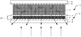
- the dimming element 1 includes a third transparent electrode 6 disposed opposite to the second transparent electrode 5, and a polymer dispersed liquid crystal layer 7 disposed between the third transparent electrode 6 and the second transparent electrode 5, the third transparent electrode 6 Located on a side of the second transparent electrode 5 facing away from the first transparent electrode 4;
- a control element is connected to the first transparent electrode 4 and the third transparent electrode 6 for applying a voltage to the first transparent electrode 4 and the third transparent electrode 6.
- the voltage on the second transparent electrode 5 decreases as the resistivity of the photosensitive layer 3 corresponding to the position of the second transparent electrode 5 increases.
- the light transmittance of the polymer dispersed liquid crystal layer 7 of each sub-region increases as the voltage difference between the second transparent electrode 5 and the third transparent electrode 6 corresponding to the position increases.
- the optical sensor element 2 and the dimming element 1 are formed between the first substrate 8 and the second substrate 9.
- the working process of the optical structure is:
- the first type as shown in FIG. 2 and FIG. 3, the controllable switch 10 is in an off state, and the automatic adjustment mode is
- the voltage applied to the first transparent electrode 4 and the third transparent electrode 6 is controlled to be a high voltage.
- the photosensitive layer 3 When the ambient light intensity is weak, the photosensitive layer 3 is in a high resistivity state, causing the voltage on the second transparent electrode 5 to be a low voltage, and the second transparent electrode 5 and the third transparent electrode 6 have a pressure difference, resulting in polymer dispersed liquid crystal.
- the liquid crystal droplets in the layer 7 rotate, and the light transmittance of the light modulating element 1 is high, so that the light transmittance of the optical structure is high;
- the photosensitive layer 3 When the ambient light intensity is strong, the photosensitive layer 3 is in a low resistivity state, causing the voltage on the second transparent electrode 5 to be a high voltage, and the second transparent electrode 5 and the third transparent electrode 6 are not in a pressure difference, resulting in polymer dispersion.
- the liquid crystal droplets in the liquid crystal layer 7 are freely oriented, and the light transmittance of the light modulating element 1 is low, so that the light transmittance of the optical structure is low.
- the second type as shown in FIG. 4 and FIG. 5, the controllable switch 10 is in a conducting state, and the manual adjustment mode is
- the voltage applied to the first transparent electrode 4 is controlled to be a low voltage, the optical sensing element 2 is in a closed state, and the voltage on the second transparent electrode 5 is also a low voltage.
- the voltage applied to the third transparent electrode 6 can be manually adjusted to adjust the voltage difference between the second transparent electrode 5 and the third transparent electrode 6, thereby controlling the rotation of the liquid crystal droplets in the polymer dispersed liquid crystal layer 7, thereby realizing manual operation. Adjust the light transmission rate of the optical structure.
- the voltage applied to the third transparent electrode 6 it is also possible to directly control the voltage applied to the third transparent electrode 6 to be a high voltage, and the second transparent electrode 5 and the third transparent electrode 6 have a pressure difference, causing the polymer to disperse the liquid crystal microcrystal in the liquid crystal layer 7.
- the light transmittance of the dimming element 1 is high.
- the light transmittance of the optical film layer 7 can be controlled to be partitioned.
- the voltage on the second transparent electrode 5 of each optical sensing element 2 increases as the ambient light intensity of the corresponding sub-region of the second transparent electrode 5 increases, thereby further
- the voltage difference between the second transparent electrode 5 and the third transparent electrode 6 decreases as the ambient light intensity of the sub-region corresponding to the second transparent electrode 5 increases, and the light transmittance of the sub-region is controlled according to the environment.
- the light intensity decreases as it increases.
- the light transmittance of the entire optical film layer 7 can be controlled to be the same, and when the ambient light intensities of different sub-regions are different, the light transmittance of the entire optical structure is the same.
- problems such as white spots or uneven brightness of the planar illumination product can be improved.
- the working principle of the present disclosure is specifically described by taking the optical sensing element to convert an ambient light intensity signal into a resistivity signal as an example. It can be understood that the optical sensing element can also convert the ambient light intensity signal into a device of other signals, such as a thin film transistor, when the light of different ambient light intensity illuminates the channel of the thin film transistor, the light leakage of the thin film transistor The current is different, thereby converting the ambient light intensity signal into a thin film transistor light leakage current.
- a mating dimming element structure is further provided to control the light transmittance of the dimming element based on parameters related to ambient light intensity acquired by the optical sensing element. In order to increase flexibility, the optical sensing element can also be turned off according to the user's instruction, and the light transmittance of the dimming element can be manually adjusted.
- Some embodiments of the present disclosure further provide a display device using the optical structure as described above, the optical structure being disposed on a display side of the display panel to automatically adjust the light transmittance of the optical structure according to the ambient light intensity, Improve the user experience.
- the partition control can adjust the light transmittance of different regions of the display device, so that the light transmittance of the entire optical structure is the same, and overcome the problem that the light intensity of different ambient environments affects the display quality in different regions of the display product.
- the optical structure of the present disclosure can also be applied to an electronic device, and can reduce the light transmittance of the optical structure when the ambient light intensity is strong, and can be used to delay the aging degree and time of the electronic device due to illumination. It is also possible to increase the light transmittance of the optical structure when the ambient light intensity is strong, and to improve the light utilization rate and be more flexible.
- the electronic device can be, for example, a lighting device, the illumination device comprising a light source, the optical structure being disposed on a light exiting side of the light source, the light emitted by the light source exiting through the optical structure.
- the partition control can achieve the same light transmittance of the entire optical structure, and improve the white point or uneven brightness of the planar illumination product.
- the optical structure can also be used only as a glass, such as on a window, a building. It can also be applied to automobiles, in particular, the window glass of an automobile adopts the optical structure of the present disclosure.
- some embodiments of the present disclosure provide a method for controlling an optical structure, including:
- the light transmittance of the corresponding sub-area is controlled according to parameters related to the ambient light intensity of each sub-area.
- the above control method automatically controls the light transmittance of the optical structure according to the ambient light intensity to improve the user experience.
- the zoning control is performed on the dimming element, and the light transmittance of the corresponding sub-area is controlled according to the parameters related to the ambient light intensity of each sub-area, so that the light transmittance of the entire dimming element can be ensured to be the same. Good user experience.
- the light transmittance of the optical structure is adjusted by adjusting the light transmittance of the light control element 1.
- obtaining parameters related to the ambient light intensity of the illumination device 1 is actually converting the ambient light intensity signal into other signals, such as a current signal, a voltage signal, and the like.
- the optical sensing element 2 includes a photosensitive layer 3, and the resistivity of the photosensitive layer 3 decreases as the ambient light intensity increases, the control method being specifically based on the resistivity of the photosensitive layer. To control the light transmittance of the dimming element.
- the specific structure of the optical sensing element 2 is described in the above embodiment, and will not be described in detail herein.
- the photosensitive layer 3 may be made of a material including selenium, aluminum sulfide, lead sulfide, barium sulfide or cadmium sulfide, and the electrical resistivity thereof decreases as the ambient light intensity increases.
- control process of the optical structure of the present disclosure will be specifically described below by taking the ambient light intensity signal into a resistivity signal as an example.
- controlling the light transmittance of the corresponding sub-region according to the ambient light intensity of each sub-area including:
- the light transmittance of the sub-region is adjusted by applying a first voltage to the first transparent electrode and the third transparent electrode of each sub-region and controlling a second voltage of the second electrode corresponding to the sub-region.
- the first voltage is applied to the first transparent electrode and the third transparent electrode, and the control is performed.
- a second voltage on the second transparent electrode corresponding to the sub-region changes in a direction close to a value of the first voltage, so that a voltage difference between the first voltage and the second voltage is decreased to reduce the sub-region Light transmission rate.
- the resistivity of the photosensitive layer 3 corresponding to the sub-area is greater than the second set value.
- a transparent electrode 4 and a third transparent electrode 6 apply a first voltage, and a voltage on the second transparent electrode 5 corresponding to the sub-region is controlled to be a second voltage, and a voltage difference between the first voltage and the second voltage controls the sub-voltage The light transmission rate of the area increases.
- the resistivity of the photosensitive layer 3 corresponding to the sub-area is less than the second set value
- a transparent electrode 4 and a third transparent electrode 6 apply a first voltage
- a voltage on the second transparent electrode 5 corresponding to the sub-region is controlled to be a second voltage
- a voltage difference between the first voltage and the second voltage controls the sub-voltage The light transmission rate of the area is reduced.
- the light transmittance of the sub-area is controlled to increase.
- the light transmittance of the sub-area is reduced, and the light transmittance of the entire optical structure can be made the same.
- the first voltage applied to the first transparent electrode and the third transparent electrode may specifically be a high voltage. Then, when the ambient light intensity of a sub-area of the illumination dimming element is less than the first set value, the resistivity of the photosensitive layer corresponding to the sub-area is greater than the second set value, and the second on the second transparent electrode can be controlled.
- the voltage is a low voltage, so that there is a pressure difference between the second transparent electrode and the third transparent electrode, thereby controlling the rotation of the liquid crystal droplets of the polymer dispersed liquid crystal layer of the sub-region, and the light transmittance is increased.
- the resistivity of the photosensitive layer corresponding to the sub-area is less than the second set value, and the second voltage on the second transparent electrode can be controlled.
- the high voltage is such that there is no pressure difference between the second transparent electrode and the third transparent electrode, thereby controlling the free orientation of the liquid crystal droplets of the polymer dispersed liquid crystal layer of the sub-region, and the light transmittance is reduced.
- the first voltage is a high voltage, which means that the first voltage has a large absolute value, and when the voltage difference between the second transparent electrode and the third transparent electrode is equal to the first voltage, The liquid crystal droplets of the polymer dispersed liquid crystal layer are controlled to rotate, so that the polymer dispersed liquid crystal layer is in a transparent state.
- control method for setting the optical structure in some embodiments of the present disclosure further includes:
- the ambient light intensity of a sub-region of the illuminating element is greater than the first set value, applying a third voltage to the first transparent electrode and the second transparent electrode, and applying the third transparent electrode according to a user's instruction.
- the fourth voltage, the differential pressure of the third voltage and the fourth voltage controls the light transmittance of the optical film layer to increase.
- the resistivity of the photosensitive layer changes even under different ambient light intensities, and the voltage on the second transparent electrode is always the same as the voltage on the first transparent electrode. , equivalent to closing the optical sensor element.
- the voltage on the third transparent electrode can be manually adjusted to adjust the pressure difference between the second transparent electrode and the third transparent electrode to control the light transmittance of the optical film layer.
- the third voltage may be a low voltage
- the fourth voltage may be a high voltage.
- the low voltage and the high voltage are relative values, and they may be a range value, and the specific value is set according to the characteristics of the optical film layer. .
- the optical film layer as a polymer dispersed liquid crystal layer as an example, it is only necessary to set the pressure difference between the third voltage and the fourth voltage to control the rotation of the liquid crystal droplets of the polymer dispersed liquid crystal layer, and the light transmittance can be increased.
- the specific values of the third voltage and the fourth voltage are not limited herein.
- the technical solution of the present disclosure by controlling the shorting or breaking of the first transparent electrode and the second transparent electrode, it is possible to automatically adjust the light transmittance of the optical structure according to the ambient light intensity or manually adjust the light transmittance of the optical structure. Free switching between the two, more flexible, and improve the user experience. Specifically, when the first transparent electrode and the second transparent electrode are disconnected, the light transmittance of the optical structure can be automatically adjusted according to the ambient light intensity. When the first transparent electrode and the second transparent electrode are short-circuited, the voltage on the second transparent electrode is equal to the voltage on the first transparent electrode, and does not change with the change of the ambient light intensity, which is equivalent to closing the optical sensing element.
- the voltage on the third transparent electrode of the dimming element can be manually adjusted to adjust the voltage difference applied to the optical film layer of the dimming element, and the light transmittance of the optical film layer follows the second transparent electrode and The voltage differential across the third transparent electrode increases and the light transmittance of the optical structure is manually adjusted.
- the optical structure has two control modes:
- the first type combined with the automatic adjustment mode shown in Figure 2 and Figure 3.
- the first transparent electrode 4 and the second transparent electrode 5 are controlled to be turned off, and the voltage applied to the first transparent electrode 4 and the third transparent electrode 6 is controlled to be a high voltage.
- the photosensitive layer 3 When the ambient light intensity is weak, the photosensitive layer 3 is in a high resistivity state, the voltage on the second transparent electrode 5 is controlled to be a low voltage, and a pressure difference exists between the second transparent electrode 5 and the third transparent electrode 6, resulting in a polymer.
- the liquid crystal droplets in the dispersed liquid crystal layer rotate, and the light transmittance of the light modulating element 1 is high, so that the light transmittance of the optical structure is high;
- the photosensitive layer 3 When the ambient light intensity is strong, the photosensitive layer 3 is in a low resistivity state, the voltage on the second transparent electrode 5 is controlled to be a high voltage, and there is no pressure difference between the second transparent electrode 5 and the third transparent electrode 6, resulting in polymerization.
- the liquid crystal droplets in the dispersed liquid crystal layer are freely oriented, and the light transmittance of the light modulating element 1 is low, so that the light transmittance of the optical structure is low.
- the first transparent electrode 4 and the second transparent electrode 5 are controlled to be short-circuited, and the voltage applied to the first transparent electrode 4 and the second transparent electrode 5 is controlled to be a low voltage, and the optical sensing element 2 is in a closed state.
- the voltage applied to the third transparent electrode 6 can be manually adjusted to adjust the pressure difference between the second transparent electrode 5 and the third transparent electrode 6, thereby controlling the rotation of the liquid crystal droplets in the polymer dispersed liquid crystal layer, thereby realizing manual adjustment of the optical structure.
- Light transmission rate can be manually adjusted to adjust the pressure difference between the second transparent electrode 5 and the third transparent electrode 6, thereby controlling the rotation of the liquid crystal droplets in the polymer dispersed liquid crystal layer, thereby realizing manual adjustment of the optical structure. Light transmission rate.
- the voltage applied to the third transparent electrode 6 it is also possible to directly control the voltage applied to the third transparent electrode 6 to be a high voltage, and there is a pressure difference between the second transparent electrode 5 and the third transparent electrode 6, causing the polymer to disperse the liquid crystal in the liquid crystal layer.
- the droplets rotate, and the light transmittance of the dimming element 1 is high.
- the partition control enables the light transmittance of the entire optical structure to be the same.
- the voltage on the second transparent electrode 5 of each optical sensing element 2 increases as the ambient light intensity of the corresponding sub-region of the optical sensing element 2 increases, thereby further
- the voltage difference between the second transparent electrode 5 and the third transparent electrode 6 decreases as the ambient light intensity of the sub-area increases, and the light transmittance of the sub-area is controlled to decrease as the ambient light intensity increases. .
- the light transmittance of the entire optical film layer 7 can be controlled to be the same, and when the ambient light intensities of different sub-regions are different, the light transmittance of the entire optical structure is the same.
- problems such as white spots or uneven brightness of the planar illumination product can be improved.
Landscapes
- Physics & Mathematics (AREA)
- Nonlinear Science (AREA)
- Chemical & Material Sciences (AREA)
- Optics & Photonics (AREA)
- Crystallography & Structural Chemistry (AREA)
- General Physics & Mathematics (AREA)
- Mathematical Physics (AREA)
- Dispersion Chemistry (AREA)
- Liquid Crystal (AREA)
- Geometry (AREA)
- Engineering & Computer Science (AREA)
- Civil Engineering (AREA)
- Structural Engineering (AREA)
Abstract
一种光学结构及其控制方法、显示器件。光学结构包括调光元件(1)、光学传感元件(2)和控制元件(11)。调光元件(1)划分为至少两个子区域(1A,1B),通过光学传感元件(2)来获取照射调光元件(1)的每一子区域(1A,1B)的环境光强度,控制元件(11)根据照射每一子区域(1A,1B)的环境光强度控制对应的子区域(1A,1B)的光线透过率。
Description
相关申请的交叉引用
本申请主张在2017年8月9日在中国提交的中国专利申请号No.201710676551.3的优先权,其全部内容通过引用包含于此。
本公开涉及光学技术领域,特别是涉及一种光学结构及其控制方法、显示器件。
聚合物分散液晶(Polymer Dispersed Liquid Crystal,简称PDLC)是将低分子液晶与预聚物相混合,在一定条件下经聚合反应,形成微米级的液晶微滴均匀地分散在高分子网络中,再利用液晶分子的介电各向异性获得具有电光响应特性的材料。PDLC具有散射态和透明态两种工作状态,并具有一定的灰度,使其受到了广泛的关注,并有着广阔的应用前景。
PDLC器件的制备工艺简单,目前已在大面积柔性显示器、光学调制器、热敏及压敏器件、电控玻璃、光阀、投影显示、电子书等方面获得广泛应用。传统的PDLC器件在加电压之后,PDLC的液晶分子开始正常排列,光线穿过,透过率提升,但是当光照时间较长的时候,容易造成光污染,或者由于紫外光导致的被光照物品老化严重,所以需要手动调整施加在聚合物分散液晶上的电压来调整光线的透过率,操作不便。
发明内容
本公开的一些实施例中提供一种光学结构,包括:
调光元件,所述调光元件包括至少两个子区域;
至少两个光学传感元件,所述光学传感元件设置在所述调光元件的表面,且与所述子区域的位置一一对应,每一光学传感元件用于获取照射对应的所述子区域的环境光强度;以及
控制元件,与所述光学传感元件和调光元件连接,用于根据照射每一子区域的环境光强度控制对应的子区域的光线透过率。
可选的,所述光学传感元件包括:
感光层,所述感光层的电阻率随着对应的子区域的环境光强度的增加而减小;
位于感光层的两侧且正对设置的第一透明电极和第二透明电极;
其中,所述控制元件与所述第一透明电极和第二透明电极连接,用于向所述第一透明电极和第二透明电极施加电压。
可选的,所述调光元件包括:
第三透明电极和第四透明电极;
位于第三透明电极和第四透明电极之间的光学膜层,所述光学膜层的光线透过率随着第三透明电极和第四透明电极之间的电压压差的增加而增加;
其中,所述控制元件与所述第三透明电极和第四透明电极连接,用于向所述第三透明电极施加电压,将第二透明电极上的电压施加在第四透明电极上,并通过控制第二透明电极与所述第三透明电极之间的电压差以调整所述光学膜层的光线透过率。
可选的,所述第二透明电极和第四透明电极为一体结构,所述第三透明电极位于所述第二透明电极的背离所述第一透明电极的一侧。
可选的,所述光学膜层为聚合物分散液晶层。
可选的,所述光学结构还包括:
可控开关,所述可控开关的第一端与所述第一透明电极连接,第二端与所述第二透明电极连接;
其中,所述控制元件还用于控制所述可控开关导通使所述第一透明电极和第二透明电极短接,根据用户的指令向第三透明电极施加电压,并通过控制第二透明电极与所述第三透明电极之间的电压差以调整所述光学膜层的光线透过率。
可选的,所述感光层的材料包括硒、硫化铝、硫化铅、硫化铋或硫化镉。
本公开的一些实施例中还提供一种如上所述的光学结构的控制方法,包括:
获取照射所述调光元件的每一子区域的环境光强度;
根据照射每一子区域的环境光强度控制对应的子区域的光线透过率。
可选的,所述根据照射每一子区域的环境光强度控制对应的子区域的光线透过率还包括:
当照射所述调光元件的一子区域的环境光强度小于第一设定值时,所述子区域对应的感光层的电阻率大于第二设定值,向第一透明电极和第三透明电极施加第一电压,控制与所述子区域对应的第二透明电极上的电压为第二电压,以通过控制所述第一电压与第二电压的压差控制所述子区域的光线透过率增加。
可选的,所述根据照射每一子区域的环境光强度控制对应的子区域的光线透过率还包括:
当照射所述调光元件的一子区域的环境光强度大于第一设定值时,该子区域对应的感光层的电阻率小于第二设定值,向第一透明电极和第三透明电极施加第一电压,控制与该子区域对应的第二透明电极上的电压为第二电压,以通过控制所述第一电压与第二电压的压差控制所述子区域的光线透过率减小。
可选的,所述控制方法还包括:
控制第一透明电极和第二透明电极短接;
向所述第一透明电极和第二透明电极施加第三电压,根据用户的指令向第三透明电极施加第四电压,以通过调整所述第三电压和第四电压的压差控制光学膜层的光线透过率。
可选的,根据照射每一子区域的环境光强度控制对应的子区域的光线透过率,包括:
通过向每一子区域的第一透明电极和第三透明电极施加第一电压,并控制所述子区域对应的第二电极的第二电压,调整所述子区域的光线透过率。
可选的,所述控制方法还包括:
当照射所述调光元件的一子区域的环境光强度降低,以至于所述子区域对应的感光层的电阻率增加时,向第一透明电极和第三透明电极施加第一电压,控制所述子区域对应的第二透明电极上的第二电压的值向远离所述第一 电压的值的方向变化,使所述第一电压与第二电压的压差增加,以增加所述子区域的光线透过率。
可选的,所述控制方法还包括:
当照射所述调光元件的一子区域的环境光强度升高,以至于所述子区域对应的感光层的电阻率降低时,向第一透明电极和第三透明电极施加第一电压,控制所述子区域对应的第二透明电极上的第二电压向靠近所述第一电压的值的方向变化,使所述第一电压与第二电压的压差降低,以降低所述子区域的光线透过率。
可选的,所述控制方法还包括:
根据照射每一子区域的环境光强度控制对应的子区域的光线透过率,控制所述调光元件的至少两个子区域的光线透过率相同。
本公开的一些实施例中还提供一种显示器件,采用如上所述的光学结构。
为了更清楚地说明本公开实施例或相关技术中的技术方案,下面将对实施例或相关技术描述中所需要使用的附图作简单地介绍,显而易见地,下面描述中的附图仅仅是本公开的一些实施例,对于本领域普通技术人员来讲,在不付出创造性劳动性的前提下,还可以根据这些附图获得其他的附图。
图1表示本公开一些实施例中光学结构的结构示意图;
图2表示本公开一些实施例中光学结构在自动调整模式下透光时的工作示意图;
图3表示本公开一些实施例中光学结构在自动调整模式下不透光时的工作示意图;
图4表示本公开一些实施例中光学结构在手动调整模式下透光时的工作示意图;
图5表示本公开一些实施例中光学结构在手动调整模式下不透光时的工作示意图。
下面将结合附图和实施例,对本公开的具体实施方式作进一步详细描述。以下实施例用于说明本公开,但不用来限制本公开的范围。
结合图1-图3所示,本公开的一些实施例提供一种光学结构,包括:
调光元件1,调光元件1包括至少两个子区域1A、1B;
至少两个光学传感元件2A、2B,光学传感元件2设置在调光元件1的表面,且与所述子区域的位置一一对应,每一光学传感元件2用于获取照射对应的所述子区域的环境光强度相关的参数;
控制元件11,与光学传感元件2和调光元件1连接,用于根据照射每一子区域的环境光强度相关的参数控制对应的子区域的光线透过率。
上述光学结构通过设置光学传感元件来获取与环境光强度相关的参数,并根据与环境光强度相关的参数来控制调光元件的光线透过率,从而能够根据环境光强度自动调整光学结构的光线透过率,无需手动调整,提高用户体验。同时,对调光元件进行分区控制,根据照射每一子区域的环境光强度相关的参数来控制对应的子区域的光线透过率,可以保证整个调光元件的光线透过率相同,获得更好的用户体验。
本公开的技术方案能够在环境光环境光强度较强时,减小光学结构的光线透过率,可以用于延缓被光照物品的老化程度和时间。还能够在环境光强度较弱时,增加光学结构的光线透过率,提高光线利用率,更加灵活。而且通过分区控制,还能够保证整个调光元件的光线透过率相同,当应用于平面照明产品上时,能够改善白点和亮度不均的问题。
需要说明的是,本公开中通过调整调光元件1的光线透过率来调整光学结构的光线透过率。
本公开的光学结构适用于照明产品和显示产品,也适用于建筑玻璃、汽车玻璃、产品橱窗等。
其中,光学传感元件2用于获取照射调光元件1的对应的子区域的环境光强度相关的参数,实际上是将环境光强度信号转换为其它信号,如:电流信号、电压信号等。
本公开的一些实施例中,光学传感元件2将环境光强度信号转换为电阻率信号,则,光学传感元件2包括:
感光层3,感光层3的电阻率随着对应的子区域的环境光强度的增加而减小;
位于感光层3的两侧且正对设置的第一透明电极4和第二透明电极5。
则,所述控制元件与第一透明电极4和第二透明电极5连接,用于向第一透明电极4和第二透明电极5施加电压。具体可以为:第一透明电极4上的电压的绝对值大于第二透明电极5上的电压的绝对值,第二透明电极5上的电压的绝对值随着与该第二透明电极5对应的感光层3的电阻率的增加而减小,所述控制元件根据第二透明电极5上的电压来控制对应的子区域的光线透过率。
其中,感光层3可以由包括硒、硫化铝、硫化铅、硫化铋或硫化镉材料制得,其电阻率随着环境光强度的增加而减小。
本公开的一些实施例中,调光元件1的具体结构可以为:
调光元件1包括:
第三透明电极6和第四透明电极;
位于第三透明电极6和第四透明电极之间的光学膜层7,光学膜层7的光线透过率随着第三透明电极6和第四透明电极之间的电压压差的增加而增加;
所述控制元件与第三透明电极6和第四透明电极连接,用于向第三透明电极6施加电压,并将第二透明电极5上的电压施加在所述第四透明电极上,通过控制第二透明电极5与第三透明电极6之间的电压差以调整光学膜层7的光线透过率。
其中,通过调整光学膜层7的光线透过率实现调整调光元件1的光线透过率。
上述技术方案的调光元件通过第二透明电极和第三透明电极的电压压差来调整光学膜层的光线透过率,从而第二透明电极上的电压能够控制光学膜层的光线透过率,由于第二透明电极上的电压随着环境光强度的增加而增加,因此,实现了根据环境光强度来自动调整调光元件的光线透过率的目的。
本公开的一些实施例中,设置所有光学传感元件2的第一透明电极4为一体结构,以简化结构,且控制简单。
可选的,设置第二透明电极5和第四透明电极为一体结构,第三透明电极6位于第二透明电极5的背离第一透明电极4的一侧,且第三透明电极6和第二透明电极5正对设置,以简化产品的结构。
调光元件1的光学膜层7具体可以为聚合物分散液晶层,光学膜层7的光线透过率大于或等于零。聚合物分散液晶是液晶与预聚物相混合,在一定条件下经聚合反应,形成微米级的液晶微滴均匀地分散在高分子网络组成的基体中,由于由液晶分子构成的小微滴的光轴处于自由取向,其折射率与基体的折射率不匹配,当光通过聚合物分散液晶时被液晶微滴强烈散射,呈不透明态,实现反光。而施加电场可调节液晶微滴的光轴取向,调整聚合物分散液晶层的透过率。当液晶微滴的折射率与基体的折射率相匹配时,呈透明态,实现透光。除去电场,液晶微滴又恢复最初的自由取向。其中,所述预聚物可以选择丙烯酸酯聚合物,丙烯酸酯聚合物的粘度较小,固化速度快,抗UV性能好,对透明导电层、玻璃和塑料有较强的附着力,能提供较好的综合性能。由丙烯酸酯聚合物和液晶制得的聚合物分散液晶具有对比度较大、驱动电压较低等优点。
在实际应用过程中,一般希望环境光强度越大,光学结构的光线透过率越小,而环境光强度越小,光学结构的光线透过率越大,以达到减少光照污染,并充分利用光线的目的。
上述技术方案中设置感光层3的电阻率随着环境光强度的增加而减小,第二透明电极5上的电压随着感光层3的电阻率的降低而增加,即,第二透明电极5上的电压随着环境光强度的增加而增加。并控制光学膜层7的光线透过率随着第二透明电极5和第三透明电极6之间的电压压差的降低而降低。
当然,本领域技术人员很容易推出,基于本公开的构思,不需要经过创造性的劳动,也能够实现光学结构的光线透过率随着环境光强度的增加而增加。例如:通过控制感光层3选择的材料,也可以实现感光层3的电阻率随着环境光强度的增加而增加,从而实现光学结构的光线透过率随着环境光强度的增加而增加。
在一个具体的实施方式中,为了实现调光元件1的光线透过率随着环境光强度的增加而减小,可以向第一透明电极4和第三透明电极6施加相同的 第一电压,且为高电压。则随着环境光强度的增加,感光层3的电阻率减小,第一透明电极4和第二透明电极5上的电压压差减小,即第二透明电极5和第三透明电极6上的电压压差减小,控制光学膜层7的光线透过率减小,实现光学膜层7的光线透过率随着环境光强度的增加而减小。
可选的,所述第一电压为固定电压,便于控制。
其中,所述第一电压为高电压是指所述第一电压绝对值较大。以光学膜层7为聚合物分散液晶为例,当第二透明电极5和第三透明电极6上的电压压差等于第一电压时,光学膜层7呈透明态。从而在环境光强度较弱时,第二透明电极5上的电压几乎为零,而第二透明电极5和第三透明电极6能够提供足够大的压差,保证光学膜层7的光线透过率较大。
需要说明的是,以上仅是将环境光强度信号转换为感光层的电阻率信号,进一步获取随着感光层的电阻率的增加而减小的电压信号,并根据该电压信号来控制光学结构的光线透过率的一种具体实现结构,本领域技术人员很容易想到获取随着感光层的电阻率的增加而减小的电压信号的结构并不局限于上述的光学传感元件的具体结构,所述调光元件也并不局限于上述具体结构,例如:还可以对电压信号进行相应处理(包括滤波电路、放大电路)后再施加到调光元件上,或利用其它电路结构将电阻率信号转换为电压信号,在此不再一一列举。
进一步地,为了提高灵活性,本公开的一些实施例中设置所述光学结构还包括:
可控开关10,所述可控开关10的第一端与所述第一透明电极4连接,第二端与所述第二透明电极5连接;
所述控制元件还用于控制所述可控开关10导通或断开,当所述可控开关10导通,所述第一透明电极4和第二透明电极5短接时,所述控制元件根据用户的指令向第三透明电极6施加电压,通过控制第二透明电极5与第三透明电极6之间的电压差以调整光学膜层7的光线透过率。
当光学膜层7为聚合物分散液晶时,其光线透过率随着第二透明电极5和第三透明电极6之间的电压压差的增加而增加。
上述光学结构包括可控开关10,通过控制所述可控开关10导通或断开, 使得光学传感元件2的第一透明电极4和第二透明电极5短接或断开。当第一透明电极4和第二透明电极5断开时,位于两者之间的感光层3的电阻率随着环境光强度的增加而减小时,会导致第二透明电极5上的电压增加,第二透明电极5和第三透明电极6上的电压压差减小,进而控制调光元件1的光线透过率,实现根据环境光强度来自动调整光学结构的光线透过率。结合图4和图5所示,而当第一透明电极4和第二透明电极5短接时,第二透明电极5上的电压等于第一透明电极4上的电压,不再随着环境光强度的变化而变化,相当于关闭光学传感元件2。此时,可以手动调整调光元件1的第三透明电极6上的电压,以调整施加在调光元件1的光学膜层7上的电压压差,光学膜层7的光线透过率随着第二透明电极5和第三透明电极6上的电压压差的增加而增加,实现手动调整光学结构的光线透过率。通过设置可控开光,使用户可以切换光学结构的光线透过率的调整模式为自动调整或手动调整,更加灵活,提高用户体验。
本公开的一些实施例中光学结构的具体结构和工作过程如下:
所述光学结构包括:
调光元件1:调光元件1包括至少两个子区域;
至少两个光学传感元件2:光学传感元件2设置在调光元件1的表面,且与所述子区域的位置一一对应。每一光学传感元件2包括正对设置的第一透明电极4和第二透明电极5,以及设置在第一透明电极4和第二透明电极5之间的感光层3,感光层3的电阻率随着环境光强度的增加而减小。第一透明电极4和第二透明电极5的两端还分别与一可控开关10的两端连接;
调光元件1包括与第二透明电极5正对设置的第三透明电极6,以及设置在第三透明电极6和第二透明电极5之间的聚合物分散液晶层7,第三透明电极6位于第二透明电极5的背离第一透明电极4的一侧;
控制元件,与第一透明电极4和第三透明电极6连接,用于向第一透明电极4和第三透明电极6施加电压。第二透明电极5上的电压随着与该第二透明电极5位置对应的感光层3的电阻率的增加而减小。每一子区域的聚合物分散液晶层7的光线透过率随着位置对应的第二透明电极5和第三透明电极6上的电压压差的增加而增加。
其中,光学传感元件2和调光元件1形成在第一基板8和第二基板9之间。
所述光学结构的工作过程为:
第一种:结合图2和图3所示,可控开关10为断开状态,自动调整模式
控制施加在第一透明电极4和第三透明电极6上的电压为高电压。
当环境光强度较弱时,感光层3处于高电阻率状态,导致第二透明电极5上的电压为低电压,第二透明电极5和第三透明电极6存在压差,导致聚合物分散液晶层7中的液晶微滴旋转,调光元件1的光线透过率较高,从而使得光学结构的光线透过率较高;
当环境光强度较强时,感光层3处于低电阻率状态,导致第二透明电极5上的电压为高电压,第二透明电极5和第三透明电极6不存在压差,导致聚合物分散液晶层7中的液晶微滴自由取向,调光元件1的光线透过率较低,从而使得光学结构的光线透过率较低。
第二种:结合图4和图5所示,可控开关10为导通状态,手动调整模式
控制施加在第一透明电极4上的电压为低电压,光学传感元件2为关闭状态,第二透明电极5上的电压也为低电压。
可以手动调整施加在第三透明电极6上的电压,来调整第二透明电极5和第三透明电极6上的电压压差,从而控制聚合物分散液晶层7中液晶微滴的旋转,实现手动调整光学结构的光线透过率。
在手动调整模式下,也可以直接控制施加在第三透明电极6上的电压为高电压,第二透明电极5和第三透明电极6存在压差,导致聚合物分散液晶层7中的液晶微滴旋转,调光元件1的光线透过率较高。
当照射在调光元件1的不同子区域的环境光强度不同时,能够分区控制光学膜层7的光线透过率。具体为:在自动调整模式下,每一光学传感元件2的第二透明电极5上的电压随着该第二透明电极5对应的子区域的环境光强度的增加而增加,进而使每一第二透明电极5与第三透明电极6上的电压压差随着该第二透明电极5对应的子区域的环境光强度的增加而减小,控制该子区域的光线透过率随着环境光强度的增加而减小。进一步地,可以控制整个光学膜层7的光线透过率相同,实现不同子区域的环境光强度不同时, 而整个光学结构的光线透过率相同。当应用于平面照明产品上时,在照明产品的光路上设置该光学结构时,能够改善平面照明产品的白点或者亮度不均等问题。
本公开的一些实施例中以所述光学传感元件将环境光强度信号转换为电阻率信号为例,来具体介绍本公开的工作原理。可以理解的是,所述光学传感元件还可以将环境光强度信号转换为其他信号的器件,例如:薄膜晶体管,当不同环境光强度的光线照射薄膜晶体管的沟道时,薄膜晶体管的光漏电流不同,从而将环境光强度信号转换为薄膜晶体管光漏电流。进而设置配合的调光元件结构,以根据光学传感元件获取的与环境光强度相关的参数来控制调光元件的光线透过率。为了提高灵活性,也可以根据用户的指令关闭光学传感元件,手动调整调光元件的光线透过率。
本公开的一些实施例中还提供一种显示器件,采用如上所述的光学结构,所述光学结构设置在显示面板的显示侧,实现根据环境光强度来自动调整光学结构的光线透过率,提高用户体验。分区控制能够对显示器件的不同区域的光线透过率进行调整,使得整个光学结构的光线透过率相同,克服显示产品的不同区域因不同的环境环境光强度影响显示质量的问题。
本公开的光学结构还可以应用在电子器件上,能够在环境光强度较强时,减小光学结构的光线透过率,可以用于延缓电子器件因被光照导致的老化程度和时间。还能够在环境光强度较强时,增加光学结构的光线透过率,提高光线利用率,更加灵活。
所述电子器件例如可以为照明器件,所述照明器件包括光源,所述光学结构设置在所述光源的出光侧,所述光源发出的光线经过所述光学结构后射出。另外,分区控制能够实现整个光学结构的光线透过率相同,改善平面照明产品的白点或者亮度不均等问题。
当然,所述光学结构还可以仅作为玻璃应用,如:应用于橱窗、建筑物上。也可以应用在汽车上,具体为,汽车的车窗玻璃采用本公开的光学结构。
结合图1-图3所示,本公开的一些实施例中提供一种光学结构的控制方法,包括:
获取照射调光元件1的每一子区域的环境光强度相关的参数;
根据照射每一子区域的环境光强度相关的参数控制对应的子区域的光线透过率。
上述控制方法根据环境光强度来自动控制光学结构的光线透过率,提高用户体验。同时,对调光元件进行分区控制,根据照射每一子区域的环境光强度相关的参数来控制对应的子区域的光线透过率,可以保证整个调光元件的光线透过率相同,获得更好的用户体验。
需要说明的是,本公开中通过调整调光元件1的光线透过率来调整光学结构的光线透过率。
其中,获取与照射所述调光元件1的环境光强度相关的参数,实际上是将环境光强度信号转换为其它信号,如:电流信号、电压信号等。
本公开的一些实施例中,光学传感元件2包括感光层3,所述感光层3的电阻率随着环境光强度的增加而减小,所述控制方法具体根据所述感光层的电阻率来控制调光元件的光线透过率。其中,光学传感元件2的具体结构参见上述实施例,在此不再详述。
具体的,所述感光层3可以由包括硒、硫化铝、硫化铅、硫化铋或硫化镉材料制得,其电阻率随着环境光强度的增加而减小。
下面以将环境光强度信号转换为电阻率信号为例,来具体介绍本公开的光学结构的控制过程。
本公开的一些实施例中,根据照射每一子区域的环境光强度控制对应的子区域的光线透过率,包括:
通过向每一子区域的第一透明电极和第三透明电极施加第一电压,并控制所述子区域对应的第二电极的第二电压,调整所述子区域的光线透过率。具体过程描述如下:
当照射所述调光元件的一子区域的环境光强度降低,以至于所述子区域对应的感光层的电阻率增加时,向第一透明电极和第三透明电极施加第一电压,控制所述子区域对应的第二透明电极上的第二电压的值向远离所述第一电压的值的方向变化,使所述第一电压与第二电压的压差增加,以增加所述子区域的光线透过率。
当照射所述调光元件的一子区域的环境光强度升高,以至于所述子区域对应的感光层的电阻率降低时,向第一透明电极和第三透明电极施加第一电压,控制所述子区域对应的第二透明电极上的第二电压向靠近所述第一电压的值的方向变化,使所述第一电压与第二电压的压差降低,以降低所述子区域的光线透过率。
本公开的一些实施例中,当照射调光元件1的一子区域的环境光强度小于第一设定值时,该子区域对应的感光层3的电阻率大于第二设定值,向第一透明电极4和第三透明电极6施加第一电压,控制与该子区域对应的第二透明电极5上的电压为第二电压,所述第一电压与第二电压的压差控制该子区域的光线透过率增加。
本公开的一些实施例中,当照射调光元件1的一子区域的环境光强度大于第一设定值时,该子区域对应的感光层3的电阻率小于第二设定值,向第一透明电极4和第三透明电极6施加第一电压,控制与该子区域对应的第二透明电极5上的电压为第二电压,所述第一电压与第二电压的压差控制该子区域的光线透过率减小。
上述控制方法,在照射一子区域的环境光强度较强时,控制该子区域的光线透过率增加。而在照射一子区域的环境光强度较强时,控制该子区域的光线透过率减小,能够实现整个光学结构的光线透过率相同。
上述控制方法中,向所述第一透明电极和第三透明电极施加的第一电压具体可以为高电压。则,当照射调光元件的一子区域的环境光强度小于第一设定值时,该子区域对应的感光层的电阻率大于第二设定值,能够控制第二透明电极上的第二电压为低电压,使得第二透明电极和第三透明电极之间存在压差,从而控制该子区域的聚合物分散液晶层的液晶微滴旋转,光线透过率增加。而当照射调光元件的一子区域的环境光强度大于第一设定值时,该子区域对应的感光层的电阻率小于第二设定值,能够控制第二透明电极上的第二电压为高电压,使得第二透明电极和第三透明电极之间不存在压差,从而控制该子区域的聚合物分散液晶层的液晶微滴自由取向,光线透过率减小。
根据上面的描述可知,所述第一电压为高电压是指所述第一电压绝对值较大,当所述第二透明电极和第三透明电极上的电压压差等于第一电压时, 能够控制聚合物分散液晶层的液晶微滴旋转,使聚合物分散液晶层呈透明态。
进一步地,为了提高灵活性,本公开的一些实施例中设置所述光学结构的控制方法还包括:
控制第一透明电极和第二透明电极短接;
当照射所述调光元件的一子区域的环境光强度大于第一设定值时,向所述第一透明电极和第二透明电极施加第三电压,根据用户的指令向第三透明电极施加第四电压,所述第三电压和第四电压的压差控制光学膜层的光线透过率增加。
上述控制方法,通过短接第一透明电极和第二透明电极,使得感光层的电阻率即使在不同环境光强度下发生变化,第二透明电极上的电压始终与第一透明电极上的电压相同,相当于关闭了光学传感元件。此时,可以手动调整第三透明电极上的电压,以调整第二透明电极和第三透明电极上的压差,来控制光学膜层的光线透过率。
其中,第三电压具体可以为低电压,第四电压具体可以为高电压,低电压和高电压是相对来说,它们可以是一个范围值,具体的取值根据光学膜层的特性来设定。以所述光学膜层为聚合物分散液晶层为例,只需要设置所述第三电压和第四电压的压差能够控制聚合物分散液晶层的液晶微滴旋转,光线透过率增加即可,第三电压和第四电压的具体取值在此不作限定。
本公开的技术方案,通过控制第一透明电极和第二透明电极短接或断开,能够实现根据环境光强度来自动调整光学结构的光线透过率或手动调整光学结构的光线透过率之间的自由切换,更加灵活,提高用户体验。具体的,当第一透明电极和第二透明电极断开时,能够根据环境光强度自动调整光学结构的光线透过率。当第一透明电极和第二透明电极短接时,第二透明电极上的电压等于第一透明电极上的电压,不再随着环境光强度的变化而变化,相当于关闭光学传感元件,此时,可以手动调整调光元件的第三透明电极上的电压,以调整施加在调光元件的光学膜层上的电压压差,光学膜层的光线透过率随着第二透明电极和第三透明电极上的电压压差的增加而增加,实现手动调整光学结构的光线透过率。
结合图1-图3所示,本公开的一些实施例中光学结构的具体控制过程为:
所述光学结构具有两种控制模式:
第一种:结合图2和图3所示,自动调整模式
控制第一透明电极4和第二透明电极5断开,并控制施加在第一透明电极4和第三透明电极6上的电压为高电压。
当环境光强度较弱时,感光层3处于高电阻率状态,控制第二透明电极5上的电压为低电压,第二透明电极5和第三透明电极6之间存在压差,导致聚合物分散液晶层中的液晶微滴旋转,调光元件1的光线透过率较高,从而使得光学结构的光线透过率较高;
当环境光强度较强时,感光层3处于低电阻率状态,控制第二透明电极5上的电压为高电压,第二透明电极5和第三透明电极6之间不存在压差,导致聚合物分散液晶层中的液晶微滴自由取向,调光元件1的光线透过率较低,从而使得光学结构的光线透过率较低。
第二种:结合图4和图5所示,手动调整模式
控制第一透明电极4和第二透明电极5短接,并控制施加在第一透明电极4和第二透明电极5上的电压为低电压,光学传感元件2为关闭状态。
可以手动调整施加在第三透明电极6上的电压,来调整第二透明电极5和第三透明电极6的压差,从而控制聚合物分散液晶层中液晶微滴的旋转,实现手动调整光学结构的光线透过率。
在手动调整模式下,也可以直接控制施加在第三透明电极6上的电压为高电压,第二透明电极5和第三透明电极6之间存在压差,导致聚合物分散液晶层中的液晶微滴旋转,调光元件1的光线透过率较高。
当照射在调光元件1的不同子区域的环境光强度不同时,分区控制能够实现整个光学结构的光线透过率相同。具体为:在自动调整模式下,每一光学传感元件2的第二透明电极5上的电压随着该光学传感元件2对应的子区域的环境光强度的增加而增加,进而使每一第二透明电极5与第三透明电极6上的电压压差随着该子区域的环境光强度的增加而减小,控制该子区域的光线透过率随着环境光强度的增加而减小。进一步地,可以控制整个光学膜层7的光线透过率相同,实现不同子区域的环境光强度不同时,而整个光学结构的光线透过率相同。当应用于平面照明产品上时,在照明产品的光路上 设置该光学结构时,能够改善平面照明产品的白点或者亮度不均等问题。
以上所述仅是本公开的一些实施方式,应当指出,对于本技术领域的普通技术人员来说,在不脱离本公开技术原理的前提下,还可以做出若干改进和替换,这些改进和替换也应视为本公开的保护范围。
Claims (16)
- 一种光学结构,包括:调光元件,所述调光元件包括至少两个子区域;至少两个光学传感元件,所述光学传感元件设置在所述调光元件的表面,且与所述子区域的位置一一对应,每一光学传感元件用于获取照射对应的所述子区域的环境光强度;以及控制元件,与所述光学传感元件和调光元件连接,用于根据照射每一子区域的环境光强度控制对应的子区域的光线透过率。
- 根据权利要求1所述的光学结构,其中,所述光学传感元件包括:感光层,所述感光层的电阻率随着对应的子区域的环境光强度的增加而减小;位于感光层的两侧且正对设置的第一透明电极和第二透明电极;其中,所述控制元件与所述第一透明电极和第二透明电极连接,用于向所述第一透明电极和第二透明电极施加电压。
- 根据权利要求2所述的光学结构,其中,所述调光元件包括:第三透明电极和第四透明电极;位于第三透明电极和第四透明电极之间的光学膜层,所述光学膜层的光线透过率随着第三透明电极和第四透明电极之间的电压压差的增加而增加;其中,所述控制元件与所述第三透明电极和第四透明电极连接,用于向所述第三透明电极施加电压,将第二透明电极上的电压施加在第四透明电极上,并通过控制第二透明电极与所述第三透明电极之间的电压差以调整所述光学膜层的光线透过率。
- 根据权利要求3所述的光学结构,其中,所述第二透明电极和第四透明电极为一体结构,所述第三透明电极位于所述第二透明电极的背离所述第一透明电极的一侧。
- 根据权利要求4所述的光学结构,其中,所述光学膜层为聚合物分散液晶层。
- 根据权利要求4所述的光学结构,还包括:可控开关,所述可控开关的第一端与所述第一透明电极连接,第二端与所述第二透明电极连接;其中,所述控制元件还用于控制所述可控开关导通使所述第一透明电极和第二透明电极短接,根据用户的指令向第三透明电极施加电压,并通过控制第二透明电极与所述第三透明电极之间的电压差以调整所述光学膜层的光线透过率。
- 根据权利要求2所述的光学结构,其中,所述感光层的材料包括硒、硫化铝、硫化铅、硫化铋或硫化镉。
- 一种权利要求1-7任一项所述的光学结构的控制方法,包括:获取照射所述调光元件的每一子区域的环境光强度;根据照射每一子区域的环境光强度控制对应的子区域的光线透过率。
- 根据权利要求8所述的控制方法,其中,所述根据照射每一子区域的环境光强度控制对应的子区域的光线透过率还包括:当照射所述调光元件的一子区域的环境光强度小于第一设定值时,所述子区域对应的感光层的电阻率大于第二设定值,向第一透明电极和第三透明电极施加第一电压,控制与所述子区域对应的第二透明电极上的电压为第二电压,以通过控制所述第一电压与第二电压的压差控制所述子区域的光线透过率增加。
- 根据权利要求8所述的控制方法,其中,所述根据照射每一子区域的环境光强度控制对应的子区域的光线透过率还包括:当照射所述调光元件的一子区域的环境光强度大于第一设定值时,该子区域对应的感光层的电阻率小于第二设定值,向第一透明电极和第三透明电极施加第一电压,控制与该子区域对应的第二透明电极上的电压为第二电压,以通过控制所述第一电压与第二电压的压差控制所述子区域的光线透过率减小。
- 根据权利要求8所述的控制方法,还包括:控制第一透明电极和第二透明电极短接;向所述第一透明电极和第二透明电极施加第三电压,根据用户的指令向第三透明电极施加第四电压,以通过调整所述第三电压和第四电压的压差控 制光学膜层的光线透过率。
- 据权利要求8所述的控制方法,其中,根据照射每一子区域的环境光强度控制对应的子区域的光线透过率,包括:通过向每一子区域的第一透明电极和第三透明电极施加第一电压,并控制所述子区域对应的第二电极的第二电压,调整所述子区域的光线透过率。
- 据权利要求12所述的控制方法,还包括:当照射所述调光元件的一子区域的环境光强度降低,以至于所述子区域对应的感光层的电阻率增加时,向第一透明电极和第三透明电极施加第一电压,控制所述子区域对应的第二透明电极上的第二电压的值向远离所述第一电压的值的方向变化,使所述第一电压与第二电压的压差增加,以增加所述子区域的光线透过率。
- 据权利要求12所述的控制方法,还包括:当照射所述调光元件的一子区域的环境光强度升高,以至于所述子区域对应的感光层的电阻率降低时,向第一透明电极和第三透明电极施加第一电压,控制所述子区域对应的第二透明电极上的第二电压向靠近所述第一电压的值的方向变化,使所述第一电压与第二电压的压差降低,以降低所述子区域的光线透过率。
- 根据权利要求8所述的控制方法,还包括:根据照射每一子区域的环境光强度控制对应的子区域的光线透过率,控制所述调光元件的至少两个子区域的光线透过率相同。
- 一种显示器件,包括权利要求1-7任一项所述的光学结构。
Priority Applications (2)
| Application Number | Priority Date | Filing Date | Title |
|---|---|---|---|
| EP18844878.1A EP3667403A4 (en) | 2017-08-09 | 2018-05-17 | OPTICAL STRUCTURE, CONTROL PROCEDURES FOR IT AND DISPLAY COMPONENTS |
| US16/340,585 US10782548B2 (en) | 2017-08-09 | 2018-05-17 | Optical structure and method for controlling the same, display device |
Applications Claiming Priority (2)
| Application Number | Priority Date | Filing Date | Title |
|---|---|---|---|
| CN201710676551.3A CN107255877B (zh) | 2017-08-09 | 2017-08-09 | 一种光学结构及其控制方法、显示器件 |
| CN201710676551.3 | 2017-08-09 |
Publications (1)
| Publication Number | Publication Date |
|---|---|
| WO2019029219A1 true WO2019029219A1 (zh) | 2019-02-14 |
Family
ID=60026848
Family Applications (1)
| Application Number | Title | Priority Date | Filing Date |
|---|---|---|---|
| PCT/CN2018/087255 Ceased WO2019029219A1 (zh) | 2017-08-09 | 2018-05-17 | 一种光学结构及其控制方法、显示器件 |
Country Status (4)
| Country | Link |
|---|---|
| US (1) | US10782548B2 (zh) |
| EP (1) | EP3667403A4 (zh) |
| CN (1) | CN107255877B (zh) |
| WO (1) | WO2019029219A1 (zh) |
Cited By (1)
| Publication number | Priority date | Publication date | Assignee | Title |
|---|---|---|---|---|
| CN114624912A (zh) * | 2022-03-22 | 2022-06-14 | 武汉华星光电技术有限公司 | 显示装置及其亮度调节方法 |
Families Citing this family (6)
| Publication number | Priority date | Publication date | Assignee | Title |
|---|---|---|---|---|
| CN107255877B (zh) | 2017-08-09 | 2021-04-13 | 京东方科技集团股份有限公司 | 一种光学结构及其控制方法、显示器件 |
| CN108107638B (zh) * | 2018-01-03 | 2020-12-18 | 京东方科技集团股份有限公司 | 感光显示面板和感光显示装置 |
| CN108336122A (zh) * | 2018-03-30 | 2018-07-27 | 深圳力合光电传感股份有限公司 | 一种显示模块、显示系统及显示系统制作方法 |
| CN109696776B (zh) * | 2019-03-12 | 2021-03-05 | 京东方科技集团股份有限公司 | 调光面板及其控制方法、显示装置 |
| CN110456540B (zh) * | 2019-08-29 | 2022-03-18 | 京东方科技集团股份有限公司 | 调光器件及使用方法、制作方法、车窗、车载后视镜和汽车 |
| CN111045263B (zh) * | 2020-01-02 | 2022-08-09 | 京东方科技集团股份有限公司 | 可调光面板、控制方法、控制器、可调光装置 |
Citations (6)
| Publication number | Priority date | Publication date | Assignee | Title |
|---|---|---|---|---|
| US20110255035A1 (en) * | 2007-06-22 | 2011-10-20 | Chiefway Engineering Co., Ltd. | Light-regulation membrane |
| CN204832719U (zh) * | 2015-06-12 | 2015-12-02 | 芜湖瑞泰精密机械有限公司 | 一种智能调光玻璃 |
| CN105929576A (zh) * | 2016-07-04 | 2016-09-07 | 京东方科技集团股份有限公司 | 一种调光装置及其控制方法、车载设备及其控制方法 |
| CN106200187A (zh) * | 2016-07-07 | 2016-12-07 | 京东方科技集团股份有限公司 | 可调光玻璃、可控遮光装置、方法和车辆 |
| CN205899213U (zh) * | 2016-08-19 | 2017-01-18 | 京东方科技集团股份有限公司 | 一种显示装置 |
| CN107255877A (zh) * | 2017-08-09 | 2017-10-17 | 京东方科技集团股份有限公司 | 一种光学结构及其控制方法、显示器件 |
Family Cites Families (9)
| Publication number | Priority date | Publication date | Assignee | Title |
|---|---|---|---|---|
| US6144359A (en) * | 1998-03-30 | 2000-11-07 | Rockwell Science Center | Liquid crystal displays utilizing polymer dispersed liquid crystal devices for enhanced performance and reduced power |
| JP3589395B2 (ja) * | 1999-03-29 | 2004-11-17 | シャープ株式会社 | 液晶表示装置 |
| EP1136874A1 (en) * | 2000-03-22 | 2001-09-26 | Hewlett-Packard Company, A Delaware Corporation | Projection screen |
| US20030230725A1 (en) * | 2002-01-30 | 2003-12-18 | Bravo Wong | Sensor arrangement having a capacitive light sensing circuit |
| JP4314623B2 (ja) * | 2006-12-07 | 2009-08-19 | 日東電工株式会社 | 透明導電性積層体及びタッチパネル |
| CN101521243B (zh) * | 2009-04-02 | 2014-10-15 | 友达光电股份有限公司 | 光学传感器与其制作方法以及具有光学传感器的显示面板 |
| EP2553723A2 (en) * | 2010-03-31 | 2013-02-06 | Pilkington Group Limited | Photovoltaic window assembly with solar control properties |
| CN106646984A (zh) * | 2015-07-22 | 2017-05-10 | 琦芯科技股份有限公司 | 高分子分散液晶调光结构 |
| CN106205502B (zh) * | 2016-07-18 | 2019-01-25 | 京东方科技集团股份有限公司 | 一种车载后视显示系统及其图像显示方法 |
-
2017
- 2017-08-09 CN CN201710676551.3A patent/CN107255877B/zh not_active Expired - Fee Related
-
2018
- 2018-05-17 US US16/340,585 patent/US10782548B2/en not_active Expired - Fee Related
- 2018-05-17 EP EP18844878.1A patent/EP3667403A4/en not_active Withdrawn
- 2018-05-17 WO PCT/CN2018/087255 patent/WO2019029219A1/zh not_active Ceased
Patent Citations (6)
| Publication number | Priority date | Publication date | Assignee | Title |
|---|---|---|---|---|
| US20110255035A1 (en) * | 2007-06-22 | 2011-10-20 | Chiefway Engineering Co., Ltd. | Light-regulation membrane |
| CN204832719U (zh) * | 2015-06-12 | 2015-12-02 | 芜湖瑞泰精密机械有限公司 | 一种智能调光玻璃 |
| CN105929576A (zh) * | 2016-07-04 | 2016-09-07 | 京东方科技集团股份有限公司 | 一种调光装置及其控制方法、车载设备及其控制方法 |
| CN106200187A (zh) * | 2016-07-07 | 2016-12-07 | 京东方科技集团股份有限公司 | 可调光玻璃、可控遮光装置、方法和车辆 |
| CN205899213U (zh) * | 2016-08-19 | 2017-01-18 | 京东方科技集团股份有限公司 | 一种显示装置 |
| CN107255877A (zh) * | 2017-08-09 | 2017-10-17 | 京东方科技集团股份有限公司 | 一种光学结构及其控制方法、显示器件 |
Non-Patent Citations (1)
| Title |
|---|
| See also references of EP3667403A4 * |
Cited By (1)
| Publication number | Priority date | Publication date | Assignee | Title |
|---|---|---|---|---|
| CN114624912A (zh) * | 2022-03-22 | 2022-06-14 | 武汉华星光电技术有限公司 | 显示装置及其亮度调节方法 |
Also Published As
| Publication number | Publication date |
|---|---|
| EP3667403A1 (en) | 2020-06-17 |
| EP3667403A4 (en) | 2021-05-12 |
| CN107255877A (zh) | 2017-10-17 |
| CN107255877B (zh) | 2021-04-13 |
| US10782548B2 (en) | 2020-09-22 |
| US20190250437A1 (en) | 2019-08-15 |
Similar Documents
| Publication | Publication Date | Title |
|---|---|---|
| WO2019029219A1 (zh) | 一种光学结构及其控制方法、显示器件 | |
| US11467436B2 (en) | Drive circuit and drive method for dimming glass, and dimming glass device | |
| US4868459A (en) | Method of and circuit for brightness and temperature-dependent control of an LCD illuminator | |
| TWI354163B (en) | Liquid crystal display device | |
| CN101414065B (zh) | 电控调光汽车天窗 | |
| US20200201088A1 (en) | Viewing angle control film and display device using the same | |
| CN112987398A (zh) | 显示装置 | |
| CN205845419U (zh) | 具有背光调节功能的oled显示器 | |
| CN115685602A (zh) | 视角可切换的显示装置及其驱动方法 | |
| CN211441917U (zh) | 玻璃透光度的调节装置及汽车 | |
| US20050156839A1 (en) | Field sequential display device and methods of fabricating same | |
| CN204407333U (zh) | 有机发光二极管显示面板及显示装置 | |
| CN106647016B (zh) | 一种聚合物分散液晶光导照明显示装置和照明显示设备 | |
| CN105116592A (zh) | 雾度可调的公共广告显示屏的制作方法及其结构 | |
| CN108051945A (zh) | 一种显示组件、液晶显示器和电子设备 | |
| CN221631806U (zh) | 一种低驱动电压高对比度调光器件及调光玻璃 | |
| JP2015055805A (ja) | 液晶表示装置 | |
| CN101819753B (zh) | 提高薄膜晶体管液晶显示器对比度的装置和方法 | |
| KR100735195B1 (ko) | 컬러 액정 표시 장치 | |
| CN111798802A (zh) | Mini LED背光模组及显示装置 | |
| CN205507298U (zh) | 一种智能挡光玻璃 | |
| KR20080085456A (ko) | 표시 장치 | |
| CN101364002B (zh) | 液晶显示装置及其背光模块与显示方法 | |
| WO2021197000A1 (zh) | 调光玻璃、调光模组及其工作方法 | |
| CN113454523B (zh) | 调光片、调光装置及调光片的管理方法 |
Legal Events
| Date | Code | Title | Description |
|---|---|---|---|
| 121 | Ep: the epo has been informed by wipo that ep was designated in this application |
Ref document number: 18844878 Country of ref document: EP Kind code of ref document: A1 |
|
| NENP | Non-entry into the national phase |
Ref country code: DE |
|
| ENP | Entry into the national phase |
Ref document number: 2018844878 Country of ref document: EP Effective date: 20200309 |