WO2019031234A1 - 光検出器 - Google Patents
光検出器 Download PDFInfo
- Publication number
- WO2019031234A1 WO2019031234A1 PCT/JP2018/027734 JP2018027734W WO2019031234A1 WO 2019031234 A1 WO2019031234 A1 WO 2019031234A1 JP 2018027734 W JP2018027734 W JP 2018027734W WO 2019031234 A1 WO2019031234 A1 WO 2019031234A1
- Authority
- WO
- WIPO (PCT)
- Prior art keywords
- wiring layer
- substrate
- connection portion
- layer
- electrode pad
- Prior art date
- Legal status (The legal status is an assumption and is not a legal conclusion. Google has not performed a legal analysis and makes no representation as to the accuracy of the status listed.)
- Ceased
Links
Images


Classifications
-
- G—PHYSICS
- G01—MEASURING; TESTING
- G01J—MEASUREMENT OF INTENSITY, VELOCITY, SPECTRAL CONTENT, POLARISATION, PHASE OR PULSE CHARACTERISTICS OF INFRARED, VISIBLE OR ULTRAVIOLET LIGHT; COLORIMETRY; RADIATION PYROMETRY
- G01J5/00—Radiation pyrometry, e.g. infrared or optical thermometry
- G01J5/10—Radiation pyrometry, e.g. infrared or optical thermometry using electric radiation detectors
- G01J5/20—Radiation pyrometry, e.g. infrared or optical thermometry using electric radiation detectors using resistors, thermistors or semiconductors sensitive to radiation, e.g. photoconductive devices
-
- G—PHYSICS
- G01—MEASURING; TESTING
- G01J—MEASUREMENT OF INTENSITY, VELOCITY, SPECTRAL CONTENT, POLARISATION, PHASE OR PULSE CHARACTERISTICS OF INFRARED, VISIBLE OR ULTRAVIOLET LIGHT; COLORIMETRY; RADIATION PYROMETRY
- G01J1/00—Photometry, e.g. photographic exposure meter
- G01J1/02—Details
-
- G—PHYSICS
- G01—MEASURING; TESTING
- G01J—MEASUREMENT OF INTENSITY, VELOCITY, SPECTRAL CONTENT, POLARISATION, PHASE OR PULSE CHARACTERISTICS OF INFRARED, VISIBLE OR ULTRAVIOLET LIGHT; COLORIMETRY; RADIATION PYROMETRY
- G01J5/00—Radiation pyrometry, e.g. infrared or optical thermometry
- G01J5/02—Constructional details
- G01J5/0225—Shape of the cavity itself or of elements contained in or suspended over the cavity
- G01J5/024—Special manufacturing steps or sacrificial layers or layer structures
-
- G—PHYSICS
- G01—MEASURING; TESTING
- G01J—MEASUREMENT OF INTENSITY, VELOCITY, SPECTRAL CONTENT, POLARISATION, PHASE OR PULSE CHARACTERISTICS OF INFRARED, VISIBLE OR ULTRAVIOLET LIGHT; COLORIMETRY; RADIATION PYROMETRY
- G01J5/00—Radiation pyrometry, e.g. infrared or optical thermometry
- G01J5/02—Constructional details
- G01J5/04—Casings
- G01J5/046—Materials; Selection of thermal materials
-
- H—ELECTRICITY
- H10—SEMICONDUCTOR DEVICES; ELECTRIC SOLID-STATE DEVICES NOT OTHERWISE PROVIDED FOR
- H10F—INORGANIC SEMICONDUCTOR DEVICES SENSITIVE TO INFRARED RADIATION, LIGHT, ELECTROMAGNETIC RADIATION OF SHORTER WAVELENGTH OR CORPUSCULAR RADIATION
- H10F30/00—Individual radiation-sensitive semiconductor devices in which radiation controls the flow of current through the devices, e.g. photodetectors
- H10F30/10—Individual radiation-sensitive semiconductor devices in which radiation controls the flow of current through the devices, e.g. photodetectors the devices being sensitive to infrared radiation, visible or ultraviolet radiation, and having no potential barriers, e.g. photoresistors
-
- H—ELECTRICITY
- H10—SEMICONDUCTOR DEVICES; ELECTRIC SOLID-STATE DEVICES NOT OTHERWISE PROVIDED FOR
- H10F—INORGANIC SEMICONDUCTOR DEVICES SENSITIVE TO INFRARED RADIATION, LIGHT, ELECTROMAGNETIC RADIATION OF SHORTER WAVELENGTH OR CORPUSCULAR RADIATION
- H10F39/00—Integrated devices, or assemblies of multiple devices, comprising at least one element covered by group H10F30/00, e.g. radiation detectors comprising photodiode arrays
- H10F39/10—Integrated devices
- H10F39/107—Integrated devices having multiple elements covered by H10F30/00 in a repetitive configuration, e.g. radiation detectors comprising photodiode arrays
-
- H—ELECTRICITY
- H10—SEMICONDUCTOR DEVICES; ELECTRIC SOLID-STATE DEVICES NOT OTHERWISE PROVIDED FOR
- H10F—INORGANIC SEMICONDUCTOR DEVICES SENSITIVE TO INFRARED RADIATION, LIGHT, ELECTROMAGNETIC RADIATION OF SHORTER WAVELENGTH OR CORPUSCULAR RADIATION
- H10F77/00—Constructional details of devices covered by this subclass
- H10F77/10—Semiconductor bodies
-
- H—ELECTRICITY
- H10—SEMICONDUCTOR DEVICES; ELECTRIC SOLID-STATE DEVICES NOT OTHERWISE PROVIDED FOR
- H10F—INORGANIC SEMICONDUCTOR DEVICES SENSITIVE TO INFRARED RADIATION, LIGHT, ELECTROMAGNETIC RADIATION OF SHORTER WAVELENGTH OR CORPUSCULAR RADIATION
- H10F77/00—Constructional details of devices covered by this subclass
- H10F77/40—Optical elements or arrangements
- H10F77/413—Optical elements or arrangements directly associated or integrated with the devices, e.g. back reflectors
Definitions
- the present disclosure relates to a photodetector.
- the film body includes a film body disposed on the surface of the substrate such that a gap is formed between the substrate and the surface of the substrate as a light detector, and a pair of electrode posts for supporting the film body, Is known to have a pair of wiring layers facing each other via a gap, and a resistance layer having an electric resistance depending on temperature.
- the electrode post has a cylindrical shape, and the wiring layer is electrically connected to the electrode post at a connection portion of the film body to which the electrode post is connected (for example, Patent Document 1) reference).
- this indication aims at providing a photodetector which can control that a failure arises in electrical connection in a connection part to which an electrode post is connected among film bodies.
- a photodetector includes a substrate, a light receiving unit, a first connection unit and a second connection unit, a first beam unit disposed between the light receiving unit and the first connection unit, and a light receiving unit.
- a film body disposed on the surface of the substrate such that an air gap is formed between the second beam portion and the second connection portion, and a gap is formed between the surface and the substrate;
- the first electrode pad formed, the second electrode pad formed on the surface of the substrate, and the first electrode pad and the first connection portion are disposed to support the film body, and to form the film body and the first
- a first electrode post electrically connecting to the electrode pad, and a second electrode pad and a second connecting portion are disposed to support the film body, and electrically connect the film body and the second electrode pad.
- a second electrode post connected to the film body, wherein the film body includes a first wiring layer and a second wiring layer facing each other via a gap in the light receiving portion;
- a resistive layer electrically connected to each of the first wiring layer and the second wiring layer in the light receiving portion, and the first electrode post is connected to the substrate from the first electrode pad.
- a first main body having a cylindrical shape extending toward the opposite side, a first bottom provided at an end of the first main body on the substrate side, and an end of the first main body opposite to the substrate
- the first wiring portion is provided with a first inclined surface which is inclined so as to be closer to the substrate as it is separated from the first main portion.
- the second electrode post Extending to the first connection portion through the first beam portion and reaching the inner surface of the first main body portion through the first inclined surface, and the second electrode post extends from the second electrode pad to the substrate
- a second main body having a cylindrical shape spreading toward the opposite side, and a second provided at an end of the second main body on the substrate side
- the second flange provided at the end opposite to the substrate in the second main body, and the second flange is inclined so as to be closer to the substrate as it is separated from the second main body
- the second wiring layer extends to the second connecting portion through the second beam portion, and reaches the inner surface of the second main portion through the second inclined surface.
- the first main body portion of the first electrode post has a tubular shape spreading from the first electrode pad toward the side opposite to the substrate. For this reason, stress concentration hardly occurs in the first connection portion of the film body to which the first electrode post is connected.
- stress concentration hardly occurs in the second connection portion of the film body to which the second electrode post is connected.
- a first flange portion is provided at an end portion of the first main body portion of the first electrode post opposite to the substrate. For this reason, it is hard to produce a deformation
- the first wiring layer extends to the inner surface of the first main body portion through the first inclined surface provided in the first ridge portion. For this reason, stress concentration hardly occurs in the first wiring layer itself at the first connection portion of the film body to which the first electrode post is connected.
- the second electrode post and in the second connection portion of the film body to which the second electrode post is connected, stress concentration does not easily occur in the second wiring layer itself. As described above, according to this photodetector, it is possible to suppress the occurrence of a defect in the electrical connection at the connection portion of the film body to which the electrode post is connected.
- the first wiring layer extends to the inner surface of the first main body and the inner surface of the first bottom through the first inclined surface, and the second wiring layer is the second inclined surface. And the inner surface of the second bottom portion. According to this configuration, the electrical connection between the first wiring layer and the first electrode post, and the electrical connection between the second wiring layer and the second electrode post can be ensured.
- the first inclined surface is annularly provided along the outer edge of the first ridge portion
- the first wiring layer includes the first inclined surface and the first body portion.
- the inner surface is covered
- the second inclined surface is annularly provided along the outer edge of the second collar, and the second wiring layer covers the second inclined surface and the inner surface of the second main body. It is also good. According to this configuration, the electrical connection between the first wiring layer and the first electrode post, and the electrical connection between the second wiring layer and the second electrode post can be further ensured.
- the film body further includes a first insulating layer formed on the surface of the first wiring layer and the second wiring layer opposite to the substrate, and the first insulating layer is The side surface of the first wiring layer may be covered in the first connection portion, and the side surface of the second wiring layer may be covered in the second connection portion. According to this configuration, peeling of the first wiring layer at the first connection portion and peeling of the second wiring layer at the second connection portion while protecting the first wiring layer and the second wiring layer from the side opposite to the substrate. Can be prevented.
- the film body further includes a second insulating layer formed on the surface on the substrate side in the first wiring layer and the second wiring layer, and the second insulating layer has a first body.
- the resistance layer is provided to the light receiving unit, the first connection unit, and the second connection unit, and may be divided at each of the first beam unit and the second beam unit. Good. According to this configuration, since the first connection portion and the second connection portion are reinforced by the resistance layer, it is possible to more reliably make the electrical connection fail in the connection portion to which the electrode post is connected in the film body. It can be suppressed. In addition, since the resistance layer is divided at the first beam portion and the second beam portion, heat generated at the light receiving portion is suppressed from escaping through the first beam portion and the second beam portion, and as a light detector Performance can be improved.
- a photodetector capable of suppressing the occurrence of a defect in the electrical connection at the connection portion of the film body to which the electrode post is connected.
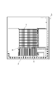
- FIG. 1 is a plan view of the photodetector of one embodiment.
- FIG. 2 is a plan view of a pixel portion of the light detector of FIG.
- FIG. 3 is a perspective view of a light detection element of the pixel unit of FIG.
- FIG. 4 is a plan view of the light detection element of FIG.
- FIG. 5 is a cross-sectional view of the light detection element of FIG. 6 is a cross-sectional view of the light detection element of FIG.
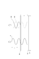
- FIG. 7 is a diagram showing the principle of the optical resonant structure.
- FIG. 8 is a view showing a method of manufacturing the light detection element of FIG.
- FIG. 9 is a view showing a method of manufacturing the light detection element of FIG. FIG.
- FIG. 10 is a diagram showing a method of manufacturing the light detection element of FIG.
- FIG. 11 is a diagram showing a method of manufacturing the light detection element of FIG.
- FIG. 12 is a diagram showing a method of manufacturing the light detection element of FIG.
- FIG. 13 is a diagram showing a method of manufacturing the light detection element of FIG.
- FIG. 14 is a diagram showing a method of manufacturing the light detection element of FIG.
- FIG. 15 is a diagram showing a method of manufacturing the light detection element of FIG.
- FIG. 16 is a diagram showing a method of manufacturing the light detection element of FIG.
- FIG. 17 is a diagram showing a method of manufacturing the light detection element of FIG.
- the photodetector 1 shown in FIG. 1 detects light by using a function as a bolometer.
- the light is, for example, infrared light including terahertz waves.
- the light detector 1 is used for an infrared imager, thermography or the like.
- the photodetector 1 has excellent characteristics for detecting light of a wavelength band of 1 ⁇ m to several tens of ⁇ m, in particular.
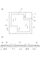
- the photodetector 1 includes a substrate 2, a pixel unit 3, a reference unit 4, and a signal processing circuit unit 5.
- the substrate 2 is, for example, a Si substrate.
- the thickness of the substrate 2 is, for example, about several hundred ⁇ m.
- the pixel unit 3, the reference unit 4, and the signal processing circuit unit 5 are formed on the substrate 2.
- the pixel unit 3 and the reference unit 4 are each electrically connected to the signal processing circuit unit 5.
- the signal processing circuit unit 5 may be formed in the substrate 2.
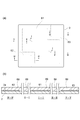
- the pixel unit 3 is configured by a plurality of light detection elements 10.
- the plurality of light detection elements 10 are arranged in a two-dimensional matrix.
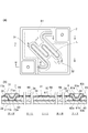
- the light detection element 10 includes a substrate 2 (more precisely, a part of the substrate 2), a light reflection layer 61, a first electrode pad 62, a second electrode pad 63, and a film.
- a body 20, a first electrode post 7 and a second electrode post 8 are provided.
- the light reflecting layer 61 is formed on the surface 2 a of the substrate 2.
- the light reflection layer 61 faces the light absorption layer 36 described later in the thickness direction of the substrate 2 (that is, the direction perpendicular to the surface 2 a of the substrate 2), and forms a light resonance structure with the light absorption layer 36. ing.
- the thickness of the light reflection layer 61 is, for example, about several hundred nm.
- the material of the light reflection layer 61 is, for example, a metal material such as Al having a high reflectance to light (for example, infrared light).
- the first electrode pad 62 and the second electrode pad 63 are formed on the surface 2 a of the substrate 2.
- the light reflection layer 61, the first electrode pad 62, and the second electrode pad 63 form, for example, a rectangular outer shape.
- the first electrode pad 62 and the second electrode pad 63 are located diagonally to the outer shape.
- Each of the first electrode pad 62 and the second electrode pad 63 has, for example, a rectangular shape when viewed from the thickness direction of the substrate 2.
- Each of the first electrode pad 62 and the second electrode pad 63 is electrically connected to the signal processing circuit unit 5 through a wire (not shown) formed on the substrate 2.
- the thickness of each of the first electrode pad 62 and the second electrode pad 63 is, for example, about several hundred nm.
- the material of each of the first electrode pad 62 and the second electrode pad 63 is, for example, a conductive metal material such as Al.
- the film body 20 is disposed on the surface 2 a of the substrate 2 so that an air gap S is formed between the film body 20 and the surface 2 a of the substrate 2.
- the film body 20 is disposed substantially parallel to the surface 2 a of the substrate 2.
- the distance between the film body 20 and the surface 2 a of the substrate 2 is, for example, about several ⁇ m.
- the film body 20 has the light receiving portion 21, the first connection portion 22 and the second connection portion 23, and the first beam portion 24 and the second beam portion 25.
- the light receiving portion 21, the first connection portion 22 and the second connection portion 23, and the first beam portion 24 and the second beam portion 25 are integrally formed and viewed from the thickness direction of the substrate 2.
- it has a rectangular outer shape.
- the first connection portion 22 and the second connection portion 23 are located diagonally of the outer shape.
- the first connection portion 22 and the second connection portion 23 each have, for example, a rectangular shape when viewed from the thickness direction of the substrate 2.
- the light receiving unit 21 faces the light reflecting layer 61 in the thickness direction of the substrate 2.
- the first connection portion 22 faces the first electrode pad 62 in the thickness direction of the substrate 2.
- the second connection portion 23 faces the second electrode pad 63 in the thickness direction of the substrate 2.
- the first beam portion 24 is disposed between the light receiving portion 21 and the first connection portion 22.
- the first beam portion 24 extends along the outer edge of the light receiving unit 21 on one side of the light receiving unit 21.
- One end of the first beam portion 24 is connected to the first connection portion 22, and the other end of the first beam portion 24 is connected to the light receiving portion 21 at a position near the second connection portion 23.
- a first slit 20 a is formed continuously between the light receiving unit 21 and the first connection unit 22 and between the light receiving unit 21 and the first beam unit 24.
- the second beam portion 25 is disposed between the light receiving portion 21 and the second connection portion 23. The second beam portion 25 extends along the outer edge of the light receiving unit 21 on the other side of the light receiving unit 21.
- One end of the second beam portion 25 is connected to the second connection portion 23, and the other end of the second beam portion 25 is connected to the light receiving portion 21 at a position near the first connection portion 22.
- a second slit 20 b is formed continuously between the light receiving unit 21 and the second connection unit 23 and between the light receiving unit 21 and the second beam unit 25.
- Each width of the first beam portion 24 and the second beam portion 25 is, for example, about several ⁇ m.
- the length of each of the first beam portion 24 and the second beam portion 25 is, for example, about several tens to several hundreds of ⁇ m.
- the width of each of the first slit 20a and the second slit 20b is, for example, about several ⁇ m.
- the first electrode post 7 is disposed between the first electrode pad 62 and the first connection portion 22.
- the first electrode post 7 supports the film body 20 and electrically connects the film body 20 and the first electrode pad 62.
- the second electrode post 8 is disposed between the second electrode pad 63 and the second connection portion 23.
- the second electrode post 8 supports the film body 20 and electrically connects the film body 20 and the second electrode pad 63.
- Each height of the 1st electrode post 7 and the 2nd electrode post 8 is about several micrometers, for example.
- the material of each of the first electrode post 7 and the second electrode post 8 is, for example, a metal material such as Ti.
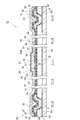
- FIG. 5 is a cross-sectional view of the light detection element 10.
- I-I, II-II, III-III, IV-IV, and V-V respectively correspond to I-I, II-II, III-III, IV-IV, and V in FIG. It is sectional drawing along -V line.
- the film body 20 includes the first wiring layer 31 and the second wiring layer 32, the first insulating layer 33 and the second insulating layer 34, the resistance layer 35, and the light absorbing layer 36. And the separation layer 37.
- the first wiring layer 31 and the second wiring layer 32 are opposed to each other via the gap G in the light receiving portion 21.
- the gap G extends along the line L.
- the line L extends in a meandering manner so as to connect, for example, the first connection portion 22 and the second connection portion 23 when viewed from the thickness direction of the substrate 2.
- the line L has a meandering portion L1.
- the meandering portion L1 includes a plurality of curved portions L2.
- the meandering portion L1 extends to one side of the light receiving portion 21 in the light receiving portion 21, for example, turns 180 ° in the curved portion L2, and extends to the other side of the light receiving portion 21, for example, 180 ° in the curved portion L2. It is configured by repeating extending to one side of the light receiving unit 21 again.
- one side is one side with respect to a straight line connecting the first connection portion 22 and the second connection portion 23 when viewed from the thickness direction of the substrate 2 (for example, the first beam portion
- the other side is the one side with respect to the straight line connecting the first connection portion 22 and the second connection portion 23. It means the opposite side (for example, the side on which the second beam 25 is present).
- one side is one side (for example, the side on which the first beam portion 24 exists) with respect to a straight line passing through the center of gravity of the film body 20 when viewed from the thickness direction of the substrate 2
- the side of the line is the side opposite to one side with respect to the straight line passing through the center of gravity of the film body 20 (the side on which the second beam 25 is present) It is also good.
- the length of each of the first wiring layer 31 and the second wiring layer 32 in the direction along the line L is, for example, several tens to several hundreds ⁇ m It is an extent.
- the width of each of the first wiring layer 31 and the second wiring layer 32 in the direction perpendicular to the line L is, for example, about several ⁇ m.
- the width of the gap G in the direction perpendicular to the line L is, for example, about several ⁇ m.
- the direction perpendicular to the line L means the direction perpendicular to the tangent at each position of the line L when viewed from the thickness direction of the substrate 2. At each position of the curvilinear portion, the direction perpendicular to the line L is different.
- the thickness of each of the first wiring layer 31 and the second wiring layer 32 is, for example, about several tens to several hundreds of nm.
- the first wiring layer 31 extends from the light receiving portion 21 to the first connection portion 22 via the first beam portion 24.
- the first wiring layer 31 is formed on the first electrode post 7 at the first connection portion 22.
- the first wiring layer 31 is electrically connected to the first electrode post 7.
- the second wiring layer 32 extends from the light receiving portion 21 to the second connection portion 23 via the second beam portion 25.
- the second wiring layer 32 is formed on the second electrode post 8 at the second connection portion 23.
- the second wiring layer 32 is electrically connected to the second electrode post 8.
- the material of each of the first wiring layer 31 and the second wiring layer 32 is, for example, a metal material such as Ti.
- the first insulating layer 33 covers the light receiving portion 21, the first beam portion 24 and the second beam portion 25 so as to cover the surface of each of the first wiring layer 31 and the second wiring layer 32 opposite to the substrate 2. And, it is formed across the first connection portion 22 and the second connection portion 23.
- the first insulating layer 33 includes the first wiring layer 31 and the first wiring layer 31 in a state in which a region along the line L is exposed in the surface of each of the first wiring layer 31 and the second wiring layer 32 opposite to the substrate 2.
- the second wiring layer 32 is formed on the surface opposite to the substrate 2.
- the second insulating layer 34 covers the surface of the first wiring layer 31 and the second wiring layer 32 on the substrate 2 side, the light receiving portion 21, the first beam portion 24 and the second beam portion 25, and The first connection portion 22 and the second connection portion 23 are formed.
- the thickness of each of the first insulating layer 33 and the second insulating layer 34 is, for example, about several tens of nm.
- the material of each of the first insulating layer 33 and the second insulating layer 34 is, for example, a silicon nitride film (SiN) or the like.
- the resistance layer 35 is formed to cover the first insulating layer 33 from the opposite side of the substrate 2 in the light receiving unit 21.
- the resistance layer 35 is in contact with a region along the line L in the surface of the first wiring layer 31 and the second wiring layer 32 opposite to the substrate 2 in the light receiving section 21. That is, the resistance layer 35 is electrically connected to each of the first wiring layer 31 and the second wiring layer 32 in the light receiving unit 21.
- the resistive layer 35 has a temperature-dependent electrical resistance.
- the thickness of the resistive layer 35 is, for example, about several tens to several hundreds of nm.
- the material of the resistance layer 35 is, for example, amorphous silicon (a-Si) or the like in which the change in electrical resistivity due to a temperature change is large.
- the light absorption layer 36 faces the surface 2 a of the substrate 2 in the light receiving unit 21.
- the light absorption layer 36 is disposed on the opposite side of the resistance layer 35 to the substrate 2. When viewed from the thickness direction of the substrate 2, the light absorption layer 36 spreads over the entire area of the light receiving unit 21.
- the thickness of the light absorption layer 36 is, for example, about ten and several nm.
- the material of the light absorption layer 36 is, for example, WSi 2 or Ti.
- the separation layer 37 is positioned between the resistance layer 35 and the light absorption layer 36 in the light receiving portion 21, and the light receiving portion 21, the first beam portion 24 and the second beam portion 25, and the first connection portion 22. And the second connection portion 23.
- the thickness of the separation layer 37 is larger than the thickness of each of the first wiring layer 31, the second wiring layer 32, the resistance layer 35, and the light absorption layer 36.
- the thickness of the separation layer 37 is, for example, about several hundred nm.
- the material of the separation layer 37 is, for example, a silicon nitride film (SiN) or the like.
- a plurality of through holes 20c and 20d are formed.
- the plurality of through holes 20 c and 20 d are holes through which an etching gas for removing a sacrificial layer 69 described later passes.
- Each of the through holes 20 c and 20 d has, for example, a circular shape when viewed in the thickness direction of the substrate 2.
- the diameter of each through hole 20c, 20d is, for example, about several ⁇ m.
- the configuration of the first electrode post 7 and the first connection portion 22 is the same as the configuration of the second electrode post 8 and the second connection portion 23, so in FIG. 6, the first electrode post 7 and the first connection portion
- the structure of 22 is shown by a code in parentheses and the description thereof is omitted.
- I--I and V--V in FIG. 6 are cross-sectional views along I--I and V--V lines in FIG. 4, respectively.
- the second electrode post 8 has a second main body 81, a second bottom 82, and a second flange 83.
- the second body portion 81, the second bottom portion 82, and the second flange portion 83 are integrally formed of a metal material such as Ti, for example.
- the second main body portion 81 has a cylindrical shape, for example, a cylindrical shape that extends from the second electrode pad 63 toward the opposite side to the substrate 2.
- Each of the inner surface 81a and the outer surface 81b of the second main body portion 81 is, for example, a truncated conical tapered surface.
- the second bottom portion 82 is provided at an end portion of the second main portion 81 on the substrate 2 side.
- the second bottom portion 82 is in contact with the second electrode pad 63.
- the inner surface 82 a of the second bottom portion 82 is, for example, a circular flat surface (flat surface parallel to the surface 2 a of the substrate 2), and is connected to the inner surface 81 a of the second main portion 81.
- the outer surface of the second bottom portion 82 is formed with a groove 82b extending annularly along the outer edge thereof.
- the groove 82 b is defined by the second bottom 82 and the second electrode pad 63.
- the second flange portion 83 is provided at an end of the second main portion 81 opposite to the substrate 2.
- the second flange portion 83 is formed in an outward flange shape.
- the surface 83a of the second ridge 83 opposite to the substrate 2 is, for example, a flat surface (flat surface parallel to the surface 2a of the substrate 2) having a circular inner edge and a rectangular outer edge, and the second body portion It is connected to the inner surface 81 a of 81.
- the surface 83b on the substrate 2 side of the second flange 83 is, for example, a flat surface (flat surface parallel to the surface 2a of the substrate 2) having a circular inner edge and a rectangular outer edge, and the outer surface of the second main body 81 It is connected with 81b.
- the outer edge of the surface 83a and the outer edge of the surface 83b are connected by the second inclined surface 83c. That is, the second inclined surface 83 c is annularly provided along the outer edge of the second flange 83.
- the second inclined surface 83c is inclined so as to be closer to the substrate 2 in the direction perpendicular to the surface 2a of the substrate 2 as it is separated from the second main body 81 in the direction parallel to the surface 2a of the substrate 2.
- the second inclined surface 83c is, for example, a tapered surface in the shape of a quadrangular pyramid.
- the second wiring layer 32 extends to the second connection portion 23 via the second beam portion 25.
- the second wiring layer 32 reaches the inner surface 81 a of the second main portion 81 and the inner surface 82 a of the second bottom portion 82 via the second inclined surface 83 c and the surface 83 a of the second flange 83 in the second connection portion 23.
- the second wiring layer 32 covers the second inclined surface 83 c and the surface 83 a of the second flange 83 and the inner surface 81 a of the second main portion 81 and the inner surface 82 a of the second bottom 82 in the second connection portion 23.
- the second wiring layer 32 is smoothly formed in the second connection portion 23 without being bent at an angle less than or equal to a right angle.
- the first insulating layer 33 covers the side surface 32 a of the second wiring layer 32 at the second connection portion 23.
- the second insulating layer 34 is the second connecting portion 23 via the surface of the second wiring layer 32 on the substrate 2 side, the surface 83 b of the second flange portion 83, and the outer surface 81 b of the second main portion 81.
- the groove 82 b is inserted on the electrode pad 63. That is, in the second connection portion 23, a part of the second insulating layer 34 is disposed between the second electrode post 8 and the second electrode pad 63.
- the resistance layer 35 is provided not only to the light receiving unit 21 but also to the second connection unit 23.
- the resistance layer 35 is not formed on the second beam portion 25 except for the both end portions. That is, the resistance layer 35 is divided at the second beam portion 25.
- each of the first electrode post 7 and the first connection portion 22 is the same as the configuration of each of the second electrode post 8 and the second connection portion 23. However, it is not the second wiring layer 32 but the first wiring layer 31 that extends to the first connection portion 22. That is, the first electrode post 7 has a first main body 71, a first bottom 72, and a first flange 73.
- the first main body portion 71, the first bottom portion 72, and the first collar portion 73 are integrally formed of a metal material such as Ti, for example.
- the first main body portion 71 has a tubular shape spreading from the first electrode pad 62 toward the opposite side to the substrate 2.
- the first bottom portion 72 is provided at an end portion of the first main portion 71 on the substrate 2 side.
- the first flange portion 73 is provided at the end of the first main portion 71 opposite to the substrate 2.
- the first flange portion 73 is provided with a first inclined surface 73 c which is inclined so as to approach the substrate 2 as it is separated from the first main portion 71.
- the first inclined surface 73 c is annularly provided along the outer edge of the first flange portion 73.
- the first wiring layer 31 extends to the first connection portion 22 via the first beam portion 24, and the inner surface 71 a of the first main portion 71 and the inner surface of the first bottom portion 72 via the first inclined surface 73 c. It has reached 72a.
- the first wiring layer 31 covers the first inclined surface 73 c and the inner surface 71 a of the first main portion 71 and the inner surface 72 a of the first bottom portion 72.
- the first insulating layer 33 covers the side surface 31 a of the first wiring layer 31 at the first connection portion 22.
- the second insulating layer 34 enters the groove 72 b formed on the outer surface of the first bottom portion 72 on the first electrode pad 62 through the outer surface 71 b of the first main portion 71.
- the resistance layer 35 is provided not only to the light receiving unit 21 but also to the first connection unit 22.
- the resistance layer 35 is not formed on the first beam portion 24 except for the both end portions. That is, the resistance layer 35 is divided at the first beam portion 24.
- the light detector 1 configured as described above detects light as follows. First, when light is incident on the light receiving unit 21, heat is generated in the light absorption layer 36 constituting an optical resonant structure described later. At this time, the light receiving unit 21 and the substrate 2 are thermally separated by the air gap S. The light receiving unit 21 and the first connection unit 22 and the first beam unit 24 are thermally separated by the first slit 20 a. Further, the light receiving portion 21 and the second connection portion 23 and the second beam portion 25 are thermally separated by the second slit 20 b. Therefore, the heat generated in the light absorbing layer 36 is dissipated to the substrate 2 side through the first beam portion 24 and the first connection portion 22 and the second beam portion 25 and the second connection portion 23. Is suppressed.
- the light absorption layer 36 and the first wiring layer 31 and the second wiring layer 32 are thermally separated by the separation layer 37. Therefore, before the heat generated in the light absorption layer 36 is sufficiently transmitted to the resistance layer 35 through the separation layer 37, the heat escapes to the substrate 2 side through the first wiring layer 31 and the second wiring layer 32. Such things are suppressed.
- the heat generated in the light absorption layer 36 is transmitted to the resistance layer 35 through the separation layer 37.
- the heat causes the resistance layer 35 to rise in temperature and to decrease in electrical resistance.
- the change in electrical resistance is sent as a signal to the signal processing circuit unit 5 through the first wiring layer 31 and the second wiring layer 32, and the first electrode post 7 and the second electrode post 8.
- the change in the electrical resistance of the resistance layer 35 is converted into a change in voltage or current.
- the change in the electrical resistance is also sent as a signal to the signal processing circuit unit 5 from the reference element of the reference unit 4.
- the change in the electrical resistance of the resistance layer of the reference element is converted into a change in voltage or current.
- the reference element is an element for compensating for temperature change due to factors other than light reception in the light detection element 10.
- the signal processing circuit unit 5 detects light based on the difference between the change in voltage or current by the light detection element 10 and the change in voltage or current by the reference element.
- part of the incident light A (having a wavelength of ⁇ ) incident on the light absorption layer 36 is reflected by the light absorption layer 36 as reflected light B1, and the other part is a light absorption layer. It passes through 36.
- the other part of the incident light A transmitted through the light absorption layer 36 is reflected by the light reflection layer 61 as a reflected light B2.
- the reflected light B1 and the reflected light B2 interfere with each other on the reflection surface of the light absorption layer 36 and are canceled.
- the incident light A is absorbed at the reflection surface of the light absorption layer 36.
- the energy of the absorbed incident light A generates heat in the light absorption layer 36.
- the absorptivity of the incident light A is determined by the sheet resistance of the light absorption layer 36 and the optical distance t between the light absorption layer 36 and the light reflection layer 61.
- the thickness of the light absorption layer 36 is set to about 16 nm (when the material of the light absorption layer 36 is WSi 2 ) so that the sheet resistance is a vacuum impedance (377 ⁇ / sq). According to this, the amplitude of the reflected light B1 reflected by the light absorption layer 36 matches the amplitude of the reflected light B2 reflected by the light reflection layer 61. For this reason, on the reflective surface of the light absorption layer 36, the reflected light B1 and the reflected light B2 are efficiently interfered and canceled. Therefore, the absorptivity of incident light A is improved.
- the light reflecting layer 61 and the light absorbing layer 36 constitute an optical resonant structure. When viewed from the thickness direction of the substrate 2, the larger the area of the overlapping portion of the light reflecting layer 61 and the light absorbing layer 36, the more efficiently the incident light A is absorbed.
- the first main body portion 71 of the first electrode post 7 has a tubular shape spreading from the first electrode pad 62 toward the opposite side to the substrate 2. Therefore, stress concentration hardly occurs in the first connection portion 22 of the film body 20. The same applies to the second electrode post 8, and stress concentration hardly occurs in the second connection portion 23. Further, a first flange portion 73 is provided in the first main body portion 71 of the first electrode post 7. Therefore, deformation does not easily occur in the first connection portion 22. The same applies to the second electrode post 8, and deformation is less likely to occur in the second connection portion 23.
- the first wiring layer 31 extends to the inner surface 71 a of the first main body portion 71 via the first inclined surface 73 c provided in the first flange portion 73. Therefore, stress concentration hardly occurs in the first wiring layer 31 itself in the first connection portion 22. The same applies to the second electrode post 8, and stress concentration hardly occurs in the second wiring layer 32 itself in the second connection portion 23. Furthermore, the first wiring layer 31 extends not only to the inner surface 71 a of the first main portion 71 but also to the inner surface 72 a of the first bottom portion 72 via the first inclined surface 73 c. Thereby, the electrical connection between the first wiring layer 31 and the first electrode post 7 can be ensured. The same applies to the second electrode post 8, and the electrical connection between the second wiring layer 32 and the second electrode post 8 can be ensured.
- the first connection portion 22 and the second connection portion 23 to which the first electrode post 7 and the second electrode post 8 are respectively connected are electrically It is possible to suppress the occurrence of connection failure. Further, according to the light detector 1, the thicknesses of the first electrode post 7 and the second electrode post 8 can be increased and the thicknesses of the first wiring layer 31 and the second wiring layer 32 can be reduced. Thereby, coexistence with reinforcement of the 1st electrode post 7 and the 2nd electrode post 8, and reduction of the heat conductance of the 1st wiring layer 31 and the 2nd wiring layer 32 can be aimed at.
- the first inclined surface 73 c is annularly provided along the outer edge of the first ridge 73
- the first wiring layer 31 includes the first inclined surface 73 c and the first main body portion.
- a second inclined surface 83c is annularly provided along the outer edge of the second flange portion 83
- the second wiring layer 32 is provided with a second inclined surface 83c and a second main body. It covers the inner surface 81 a of the portion 81. According to this configuration, the electrical connection between the first wiring layer 31 and the first electrode post 7 and the electrical connection between the second wiring layer 32 and the second electrode post 8 can be further ensured. it can.
- the first insulating layer 33 covers the side 31 a of the first wiring layer 31 and the side 32 a of the second wiring layer 32 in each of the first connection portion 22 and the second connection portion 23. ing. According to this configuration, peeling of the first wiring layer 31 in the first connection portion 22 and protection in the second connection portion 23 while protecting the first wiring layer 31 and the second wiring layer 32 from the side opposite to the substrate 2. Peeling of the second wiring layer 32 can be prevented.
- the second insulating layer 34 is formed on the first electrode pad 62 at the first connection portion 22 via the outer surface 71 b of the first main portion 71 of the first electrode post 7.
- the second insulating layer 34 is formed on the second electrode pad 63 via the outer surface 81 b of the second main portion 81 of the second electrode post 8 at the second connection portion 23.
- the groove 82b is formed in the outer surface of the second bottom 82 at the position.
- the resistance layer 35 is provided in the light receiving portion 21, the first connection portion 22 and the second connection portion 23, and is divided at each of the first beam portion 24 and the second beam portion 25. ing. According to this configuration, since the first connection portion 22 and the second connection portion 23 are reinforced by the resistance layer 35, each of the first electrode post 7 and the second electrode post 8 in the film body 20 is connected It is possible to more reliably suppress the occurrence of a defect in the electrical connection in each of the first connection portion 22 and the second connection portion 23. Further, since the resistive layer 35 is divided at the first beam portion 24 and the second beam portion 25, heat generated at the light receiving portion 21 is prevented from escaping through the first beam portion 24 and the second beam portion 25. Thus, the performance of the photodetector 1 can be improved.
- FIGS. 8 to 17 II, II-II, III-III, IV-IV and V-V of (b) respectively correspond to II line of (a), It is a cross-sectional view along the II-II line, the III-III line, the IV-IV line, and the VV line.
- FIG. 15 and FIG. 16 a diagram such as the above (a) is omitted.
- the substrate 2 is prepared, and the light reflection layer 61, the first electrode pad 62, and the second electrode pad 63 are formed on the surface 2 a of the substrate 2.
- the light reflection layer 61, the first electrode pad 62, and the second electrode pad 63 have the above-described shape by etching.
- a sacrificial layer 69 is formed on the surface 2 a of the substrate 2 so as to cover the light reflection layer 61, the first electrode pad 62, and the second electrode pad 63.
- the material of the sacrificial layer 69 is, for example, polyimide.
- through holes 69a and 69b are formed in the sacrificial layer 69 by removing a part of the sacrificial layer 69 by etching.
- the through holes 69a and 69b are formed on the first electrode pad 62 and the second electrode pad 63, respectively.
- the surfaces of the first electrode pad 62 and the second electrode pad 63 opposite to the substrate 2 are exposed.
- the inner surfaces of the through holes 69a and 69b are, for example, truncated cone-like tapered surfaces.
- the inner surfaces of the through holes 69 a and 69 b respectively extend from the first electrode pad 62 and the second electrode pad 63 toward the side opposite to the substrate 2.
- a second insulating layer 34 is formed on the sacrificial layer 69.
- the second insulating layer 34 is formed such that the inner surface thereof is, for example, a truncated conical surface in each of the through holes 69a and 69b.
- the through holes 34 a and 34 b are formed in the second insulating layer 34 by removing a part of the second insulating layer 34 by etching.
- the through holes 34 a and 34 b are respectively formed on the first electrode pad 62 and the second electrode pad 63.
- each through-hole 34a, 34b the surface on the opposite side to the board
- Each of the through holes 34 a and 34 b has a circular shape when viewed from the thickness direction of the substrate 2.
- the first electrode post 7 is formed on the second insulating layer 34 in the through hole 69a
- the second electrode post 8 is formed on the second insulating layer 34 in the through hole 69b.
- Each of the first electrode post 7 and the second electrode post 8 is formed, for example, by vapor deposition.
- the inner surfaces of the second insulating layers 34 are tapered surfaces in each of the through holes 69a and 69b, each of the first electrode post 7 and the second electrode post 8 is formed more reliably. Thereby, disconnection due to film formation failure of the first electrode post 7 and the second electrode post 8 is suppressed.
- the second insulating layer 34 has a portion in each of the first connection portion 22 and the second connection portion 23, the groove 72b and the groove 82b, respectively, the first electrode post 7 and the The tolerance for misalignment of the two-electrode post 8 is broadened.
- the first wiring layer 31 and the second wiring layer 32 are formed on the second insulating layer 34 so as to cover the first electrode post 7 and the second electrode post 8.
- Each of the first wiring layer 31 and the second wiring layer 32 is formed, for example, by vapor deposition.
- the first inclined surface 73c of the first collar 73 and the inner surface 71a of the first main body 71, and the second inclined surface 83c of the second collar 83 and the inner surface 81a of the second main body 81 have tapered surfaces.
- the first wiring layer 31 and the second wiring layer 32 are more reliably formed on the first electrode post 7 and the second electrode post 8.
- the first wiring layer 31 and the second wiring layer 32 have the above-described shape by etching.
- the light receiving unit 21, the first beam portion 24 and the second beam portion 25, and the first beam portion 24 and the second beam portion 25 are provided to cover the first wiring layer 31 and the second wiring layer 32 from the opposite side of the substrate 2.
- the first insulating layer 33 is formed across the first connection portion 22 and the second connection portion 23.
- the first insulating layer 33 has the above-described shape by etching.
- the first insulating layer 33 covers the side surface 31 a of the first wiring layer 31 and the side surface 32 a of the second wiring layer 32, the number of interfaces of different materials exposed is reduced. Thereby, in the manufacturing process of the light detection element 10, the etching defect resulting from the interface can be reduced.
- the resistance layer 35 is formed to cover the first insulating layer 33 from the opposite side of the substrate 2, and the first connection portion 22 and the second connection portion 23.
- the resistance layer 35 is formed on the first insulating layer 33 in FIG.
- the separation layer 37 is formed to cover the resistance layer 35 from the opposite side of the substrate 2, and the first beam portion 24 and the second beam In the portion 25, the separation layer 37 is formed on the first insulating layer 33.
- the light absorption layer 36 is formed on the separation layer 37, and the through holes 20 c and 20 d are further formed.
- the light absorption layer 36 is shaped as described above by etching.
- the through holes 20c and 20d are formed at the above-described positions by etching.
- the first slit 20a and the second slit 20b are formed, and etching is further advanced from the first slit 20a and the second slit 20b, and the through holes 20c and 20d, and sacrificial
- the void 69 is formed by removing the layer 69.
- the first slit 20a and the second slit 20b are formed at the above-described positions by etching.
- this indication is not limited to the embodiment mentioned above.
- the second wiring layer 32 extends to the inner surface 81 a of the second main portion 81 and the inner surface 82 a of the second bottom 82, but the second wiring layer 32 is the inner surface of the second bottom 82 It does not have to reach 82a.
- the second wiring layer 32 may extend to the inner surface 81 a of the second main portion 81 via the second inclined surface 83 c of the second flange portion 83 in the second connection portion 23.
- the first wiring layer 31 may extend to the inner surface 71 a of the first main body 71 via the first inclined surface 73 c of the first ridge 73 at the first connection portion 22.
- the second inclined surface 83c is annularly provided along the outer edge of the second flange 83 in the above embodiment, the second inclined surface 83c is, for example, at the outer edge of the second flange 83. It may be provided only in part.
- the second wiring layer 32 may not cover the second inclined surface 83 c and the inner surface 81 a of the second main portion 81 and the inner surface 72 a of the second bottom portion 82.
- the second wiring layer 32 may extend to the inner surface 81 a of the second main portion 81 via the second inclined surface 83 c.
- the first inclined surface 73 c may be provided, for example, only on a part of the outer edge of the first flange portion 73.
- the first wiring layer 31 may not cover the first inclined surface 73 c and the inner surface 71 a of the first main body 71 and the inner surface 72 a of the first bottom 72.
- the first wiring layer 31 may extend to the inner surface 71 a of the first main body 71 via the first inclined surface 73 c.
- the inner surface 81a and the outer surface 81b of the second main body portion 81 are respectively truncated cone-like tapered surfaces
- the inner surface 81a and the outer surface 81b of the second main body portion 81 are It may be a tapered surface.
- the inner surface 71a and the outer surface 71b of the first main body portion 71 may each be, for example, a tapered surface having a quadrangular pyramid shape.
- the inner edge of the surface 83a opposite to the substrate 2 in the second flange 83 is circular and the outer edge is rectangular, but the inner and outer edges of the surface 83a are, for example, circular. Or it may be rectangular.
- the inner edge of the surface 83b on the substrate 2 side in the second flange 83 is circular and the outer edge is rectangular, the inner edge and the outer edge of the surface 83b are, for example, circular or rectangular, respectively. It may be The same applies to the first collar 73, and the inner edge and the outer edge of the surface 73a may be, for example, circular or rectangular. Also, the inner edge and the outer edge of the surface 73b may be, for example, circular or rectangular.
- the film body 20 showed the example which exhibits rectangular shape, for example, when it sees from the thickness direction of the board
- the film body 20 may have various shapes such as, for example, a circular shape.
- various materials and thicknesses can be selected for each of the first wiring layer 31 and the second wiring layer 32, the resistance layer 35, the light absorption layer 36, and the separation layer 37.
- the sensitivity can be easily improved and the strength of the film body 20 can be improved. It can be improved.
- the optimum material for each of the first wiring layer 31, the second wiring layer 32, and the light absorption layer 36 it is possible to achieve both improvement in sensitivity and response speed.
- the through holes 20 c and 20 d may have various shapes such as an oval or a square. Further, the positions at which the through holes 20c and 20d are formed are not limited. The through holes 20 c and 20 d may be formed at various positions of the light receiving unit 21.
- the pixel unit 3 may be configured by one light detection element 10.
- Second electrode pad 71 First body portion 71a inner surface 71b Outer surface 72 first bottom portion 72a inner surface 72b groove 73: first ridge portion 73c: first inclined surface 81: second main body portion 81a: inner surface 81b: outer surface 82: second bottom portion 82a: inner surface 82b: groove: 83: second ridge portion 83c: second inclined surface, G: gap, S: air gap.
Landscapes
- Physics & Mathematics (AREA)
- General Physics & Mathematics (AREA)
- Spectroscopy & Molecular Physics (AREA)
- Engineering & Computer Science (AREA)
- Manufacturing & Machinery (AREA)
- Photometry And Measurement Of Optical Pulse Characteristics (AREA)
- Solid State Image Pick-Up Elements (AREA)
Abstract
光検出器は、基板と、基板の表面上に配置された膜体と、膜体を支持する第1電極ポストと、膜体を支持する第2電極ポストと、を備える。第1電極ポストは、第1電極パッドから基板とは反対側に向かって広がる筒状を呈する第1本体部と、第1本体部における基板側の端部に設けられた第1底部と、第1本体部における基板とは反対側の端部に設けられた第1鍔部と、を有する。第1鍔部には、第1本体部から離れるほど基板に近づくように傾斜した第1傾斜面が設けられている。第1配線層は、第1傾斜面を介して第1本体部の内面に至っている。第2電極ポスト及び第2配線層は、第1電極ポスト及び第1配線層と同様に形成されている。
Description
本開示は、光検出器に関する。
光検出器として、基板と、基板の表面との間に空隙が形成されるように基板の表面上に配置された膜体と、膜体を支持する一対の電極ポストと、を備え、膜体が、ギャップを介して互いに対向する一対の配線層と、温度に依存する電気抵抗を有する抵抗層と、を有するものが知られている。このような光検出器では、電極ポストが円筒状を呈しており、膜体のうち電極ポストが接続される接続部において配線層が電極ポストと電気的に接続されている(例えば、特許文献1参照)。
上述したような光検出器では、電極ポストの外面が膜体の接続部における基板側の表面と垂直に交わるため、その交わった部分で応力集中が起こり易く、その結果、膜体のうち電極ポストが接続される接続部において電気的な接続に不良が生じるおそれがある。
そこで、本開示は、膜体のうち電極ポストが接続される接続部において電気的な接続に不良が生じるのを抑制することができる光検出器を提供することを目的とする。
本開示の一側面の光検出器は、基板と、受光部、第1接続部及び第2接続部、受光部と第1接続部との間に配置された第1梁部、並びに、受光部と第2接続部との間に配置された第2梁部を有し、基板の表面との間に空隙が形成されるように基板の表面上に配置された膜体と、基板の表面に形成された第1電極パッドと、基板の表面に形成された第2電極パッドと、第1電極パッドと第1接続部との間に配置され、膜体を支持すると共に、膜体と第1電極パッドとを電気的に接続する第1電極ポストと、第2電極パッドと第2接続部との間に配置され、膜体を支持すると共に、膜体と第2電極パッドとを電気的に接続する第2電極ポストと、を備え、膜体は、受光部においてギャップを介して互いに対向する第1配線層及び第2配線層と、温度に依存する電気抵抗を有し、受光部において第1配線層及び第2配線層のそれぞれと電気的に接続された抵抗層と、を含み、第1電極ポストは、第1電極パッドから基板とは反対側に向かって広がる筒状を呈する第1本体部と、第1本体部における基板側の端部に設けられた第1底部と、第1本体部における基板とは反対側の端部に設けられた第1鍔部と、を有し、第1鍔部には、第1本体部から離れるほど基板に近づくように傾斜した第1傾斜面が設けられており、第1配線層は、第1梁部を介して第1接続部に延在しており、第1傾斜面を介して第1本体部の内面に至っており、第2電極ポストは、第2電極パッドから基板とは反対側に向かって広がる筒状を呈する第2本体部と、第2本体部における基板側の端部に設けられた第2底部と、第2本体部における基板とは反対側の端部に設けられた第2鍔部と、を有し、第2鍔部には、第2本体部から離れるほど基板に近づくように傾斜した第2傾斜面が設けられており、第2配線層は、第2梁部を介して第2接続部に延在しており、第2傾斜面を介して第2本体部の内面に至っている。
この光検出器では、第1電極ポストの第1本体部が、第1電極パッドから基板とは反対側に向かって広がる筒状を呈している。このため、膜体のうち第1電極ポストが接続される第1接続部において応力集中が起こり難い。第2電極ポストについても同様であり、膜体のうち第2電極ポストが接続される第2接続部において応力集中が起こり難い。また、第1電極ポストの第1本体部における基板とは反対側の端部に第1鍔部が設けられている。このため、膜体のうち第1電極ポストが接続される第1接続部において変形が生じ難い。第2電極ポストについても同様であり、膜体のうち第2電極ポストが接続される第2接続部において変形が生じ難い。更に、第1配線層が、第1鍔部に設けられた第1傾斜面を介して第1本体部の内面に至っている。このため、膜体のうち第1電極ポストが接続される第1接続部において第1配線層自体に応力集中が起こり難い。第2電極ポストについても同様であり、膜体のうち第2電極ポストが接続される第2接続部において第2配線層自体に応力集中が起こり難い。以上により、この光検出器によれば、膜体のうち電極ポストが接続される接続部において電気的な接続に不良が生じるのを抑制することができる。
本開示の一側面の光検出器では、第1配線層は、第1傾斜面を介して第1本体部の内面及び第1底部の内面に至っており、第2配線層は、第2傾斜面を介して第2本体部の内面及び第2底部の内面に至っていてもよい。この構成によれば、第1配線層と第1電極ポストとの電気的な接続、及び第2配線層と第2電極ポストとの電気的な接続を確実化することができる。
本開示の一側面の光検出器では、第1傾斜面は、第1鍔部の外縁に沿って環状に設けられており、第1配線層は、第1傾斜面、及び第1本体部の内面を覆っており、第2傾斜面は、第2鍔部の外縁に沿って環状に設けられており、第2配線層は、第2傾斜面、及び第2本体部の内面を覆っていてもよい。この構成によれば、第1配線層と第1電極ポストとの電気的な接続、及び第2配線層と第2電極ポストとの電気的な接続をより一層確実化することができる。
本開示の一側面の光検出器では、膜体は、第1配線層及び第2配線層における基板とは反対側の表面に形成された第1絶縁層を更に含み、第1絶縁層は、第1接続部において第1配線層の側面を覆っており、第2接続部において第2配線層の側面を覆っていてもよい。この構成によれば、第1配線層及び第2配線層を基板とは反対側から保護しつつ、第1接続部における第1配線層の剥離、及び第2接続部における第2配線層の剥離を防止することができる。
本開示の一側面の光検出器では、膜体は、第1配線層及び第2配線層における基板側の表面に形成された第2絶縁層を更に含み、第2絶縁層は、第1本体部の外面を介して、第1電極パッド上において第1底部の外面に形成された溝に入り込んでおり、第2本体部の外面を介して、第2電極パッド上において第2底部の外面に形成された溝に入り込んでいてもよい。この構成によれば、第1配線層及び第2配線層を基板側から保護しつつ、第1電極パッド上での第2絶縁層の剥離や第1電極ポストの外面の露出、及び第2電極パッド上での第2絶縁層の剥離や第2電極ポストの外面の露出を防止することができる。
本開示の一側面の光検出器では、抵抗層は、受光部、第1接続部及び第2接続部に設けられており、第1梁部及び第2梁部のそれぞれにおいて分断されていてもよい。この構成によれば、抵抗層によって第1接続部及び第2接続部が補強されるため、膜体のうち電極ポストが接続される接続部において電気的な接続に不良が生じるのをより確実に抑制することができる。また、抵抗層が第1梁部及び第2梁部において分断されているため、受光部で生じた熱が第1梁部及び第2梁部を介して逃げるのを抑制し、光検出器としての性能を向上させることができる。
本開示によれば、膜体のうち電極ポストが接続される接続部において電気的な接続に不良が生じるのを抑制することができる光検出器を提供することが可能となる。
以下、本開示の好適な実施形態について、図面を参照して詳細に説明する。なお、各図において同一又は相当部分には同一符号を付し、重複する説明を省略する。
図1に示される光検出器1は、ボロメータとしての機能を利用することで、光を検出する。当該光は、例えばテラヘルツ波を含む赤外線である。当該光が赤外線である場合、光検出器1は、赤外イメージャ、又はサーモグラフィー等に用いられる。光検出器1は、特に1μm~数十μmの波長帯域の光の検出に優れた特性を有している。図1に示されるように、光検出器1は、基板2と、画素部3と、リファレンス部4と、信号処理回路部5と、を備えている。基板2は、例えばSi基板である。基板2の厚さは、例えば数百μm程度である。画素部3、リファレンス部4、及び信号処理回路部5は、基板2上に形成されている。画素部3及びリファレンス部4は、それぞれ、信号処理回路部5と電気的に接続されている。なお、信号処理回路部5は、基板2内に形成されていてもよい。
図2に示されるように、画素部3は、複数の光検出素子10によって構成されている。複数の光検出素子10は、二次元マトリックス状に配置されている。図3に示されるように、光検出素子10は、基板2(正確には、基板2の一部)と、光反射層61と、第1電極パッド62と、第2電極パッド63と、膜体20と、第1電極ポスト7と、第2電極ポスト8と、を備えている。
光反射層61は、基板2の表面2aに形成されている。光反射層61は、基板2の厚さ方向(すなわち、基板2の表面2aに垂直な方向)において、後述する光吸収層36と対向しており、光吸収層36と共に光共振構造を構成している。光反射層61の厚さは、例えば数百nm程度である。光反射層61の材料は、例えば、光(例えば赤外線)に対する反射率が大きいAl等の金属材料である。
第1電極パッド62及び第2電極パッド63は、基板2の表面2aに形成されている。光反射層61、第1電極パッド62及び第2電極パッド63は、基板2の厚さ方向から見た場合に例えば矩形状の外形を構成している。第1電極パッド62及び第2電極パッド63は、当該外形の対角に位置している。第1電極パッド62及び第2電極パッド63は、それぞれ、基板2の厚さ方向から見た場合に例えば矩形状を呈している。第1電極パッド62及び第2電極パッド63は、それぞれ、基板2に形成された配線(図示省略)を介して、信号処理回路部5と電気的に接続されている。第1電極パッド62及び第2電極パッド63のそれぞれの厚さは、例えば数百nm程度である。第1電極パッド62及び第2電極パッド63のそれぞれの材料は、例えば、導電性を有するAl等の金属材料である。
膜体20は、基板2の表面2aとの間に空隙Sが形成されるように基板2の表面2a上に配置されている。膜体20は、基板2の表面2aと略平行に配置されている。膜体20と基板2の表面2aとの距離は、例えば数μm程度である。図3及び図4に示されるように、膜体20は、受光部21、第1接続部22及び第2接続部23、並びに、第1梁部24及び第2梁部25を有している。受光部21、第1接続部22及び第2接続部23、並びに、第1梁部24及び第2梁部25は、一体的に形成されており、基板2の厚さ方向から見た場合に例えば矩形状の外形を構成している。第1接続部22及び第2接続部23は、当該外形の対角に位置している。第1接続部22及び第2接続部23は、それぞれ、基板2の厚さ方向から見た場合に例えば矩形状を呈している。
受光部21は、基板2の厚さ方向において光反射層61と対向している。第1接続部22は、基板2の厚さ方向において第1電極パッド62と対向している。第2接続部23は、基板2の厚さ方向において第2電極パッド63と対向している。
第1梁部24は、受光部21と第1接続部22との間に配置されている。第1梁部24は、受光部21の一方の側において受光部21の外縁に沿って延在している。第1梁部24の一端は、第1接続部22と接続されており、第1梁部24の他端は、第2接続部23の近傍の位置で受光部21と接続されている。受光部21と第1接続部22との間、及び受光部21と第1梁部24との間には、第1スリット20aが一続きに形成されている。第2梁部25は、受光部21と第2接続部23との間に配置されている。第2梁部25は、受光部21の他方の側において受光部21の外縁に沿って延在している。第2梁部25の一端は、第2接続部23と接続されており、第2梁部25の他端は、第1接続部22の近傍の位置で受光部21と接続されている。受光部21と第2接続部23との間、及び受光部21と第2梁部25との間には、第2スリット20bが一続きに形成されている。第1梁部24及び第2梁部25のそれぞれの幅は、例えば数μm程度である。第1梁部24及び第2梁部25のそれぞれの長さは、例えば数十~数百μm程度である。第1スリット20a及び第2スリット20bのそれぞれの幅は、例えば数μm程度である。
第1電極ポスト7は、第1電極パッド62と第1接続部22との間に配置されている。第1電極ポスト7は、膜体20を支持すると共に、膜体20と第1電極パッド62とを電気的に接続している。第2電極ポスト8は、第2電極パッド63と第2接続部23との間に配置されている。第2電極ポスト8は、膜体20を支持すると共に、膜体20と第2電極パッド63とを電気的に接続している。第1電極ポスト7及び第2電極ポスト8のそれぞれの高さは、例えば数μm程度である。第1電極ポスト7及び第2電極ポスト8のそれぞれの材料は、例えばTi等の金属材料である。
図5は、光検出素子10の断面図である。図5のI-I、II-II、III-III、IV-IV、V-Vは、それぞれ、図4のI-I線、II-II線、III-III線、IV-IV線、V-V線に沿っての断面図である。図5に示されるように、膜体20は、第1配線層31及び第2配線層32と、第1絶縁層33及び第2絶縁層34と、抵抗層35と、光吸収層36と、分離層37と、を有している。
図4及び図5に示されるように、基板2の厚さ方向から見た場合に、第1配線層31及び第2配線層32は、受光部21においてギャップGを介して互いに対向している。ギャップGは、ラインLに沿って延在している。ラインLは、基板2の厚さ方向から見た場合に、例えば第1接続部22と第2接続部23とを結ぶように蛇行状に延在している。具体的には、ラインLは、蛇行部L1を有している。蛇行部L1は、複数の曲線部L2を含んでいる。蛇行部L1は、受光部21において、受光部21の一方の側に延び、曲線部L2において、例えば180°折り返して、受光部21の他方の側に延び、曲線部L2において、例えば180°折り返して、再び受光部21の一方の側に伸びることを繰り返すことによって構成されている。
本実施形態では、一方の側とは、基板2の厚さ方向から見た場合に、第1接続部22と第2接続部23とを結ぶ直線に対して一方の側(例えば第1梁部24が存在する側)をいい、他方の側とは、基板2の厚さ方向から見た場合に、第1接続部22と第2接続部23とを結ぶ直線に対して一方の側とは反対の側(例えば第2梁部25が存在する側)をいう。また、一方の側とは、基板2の厚さ方向から見た場合に、膜体20の重心を通る直線に対して一方の側(例えば第1梁部24が存在する側)であり、他方の側とは、基板2の厚さ方向から見た場合に、膜体20の重心を通る直線に対して一方の側とは反対の側(第2梁部25が存在する側)であってもよい。
基板2の厚さ方向から見た場合に、受光部21において、ラインLに沿った方向における第1配線層31及び第2配線層32のそれぞれの長さは、例えば、数十~数百μm程度である。基板2の厚さ方向から見た場合に、ラインLに垂直な方向における第1配線層31及び第2配線層32のそれぞれの幅は、例えば数μm程度である。基板2の厚さ方向から見た場合に、ラインLに垂直な方向におけるギャップGの幅は、例えば数μm程度である。ラインLに垂直な方向とは、基板2の厚さ方向から見た場合に、ラインLの各位置における接線に垂直な方向をいう。曲線部の各位置においては、ラインLに垂直な方向はそれぞれ相違する。第1配線層31及び第2配線層32のそれぞれの厚さは、例えば数十~数百nm程度である。
第1配線層31は、受光部21から第1梁部24を介して第1接続部22に延在している。第1配線層31は、第1接続部22において第1電極ポスト7上に形成されている。第1配線層31は、第1電極ポスト7と電気的に接続されている。第2配線層32は、受光部21から第2梁部25を介して第2接続部23に延在している。第2配線層32は、第2接続部23において第2電極ポスト8上に形成されている。第2配線層32は、第2電極ポスト8と電気的に接続されている。第1配線層31及び第2配線層32のそれぞれの材料は、例えばTi等の金属材料である。
第1絶縁層33は、第1配線層31及び第2配線層32のそれぞれにおける基板2とは反対側の表面を覆うように、受光部21、第1梁部24及び第2梁部25、並びに、第1接続部22及び第2接続部23に渡って形成されている。第1絶縁層33は、第1配線層31及び第2配線層32のそれぞれにおける基板2とは反対側の表面のうちラインLに沿った領域を露出させた状態で、第1配線層31及び第2配線層32における基板2とは反対側の表面に形成されている。第2絶縁層34は、第1配線層31及び第2配線層32のそれぞれにおける基板2側の表面を覆うように、受光部21、第1梁部24及び第2梁部25、並びに、第1接続部22及び第2接続部23に渡って形成されている。第1絶縁層33及び第2絶縁層34のそれぞれの厚さは、例えば数十nm程度である。第1絶縁層33及び第2絶縁層34のそれぞれの材料は、例えばシリコン窒化膜(SiN)等である。
抵抗層35は、受光部21において、基板2の反対側から第1絶縁層33を覆うように形成されている。抵抗層35は、受光部21において、第1配線層31及び第2配線層32のそれぞれにおける基板2とは反対側の表面のうちラインLに沿った領域に接触している。つまり、抵抗層35は、受光部21において、第1配線層31及び第2配線層32のそれぞれと電気的に接続されている。抵抗層35は、温度に依存する電気抵抗を有している。抵抗層35の厚さは、例えば数十~数百nm程度である。抵抗層35の材料は、例えば、温度変化による電気抵抗率の変化が大きいアモルファスシリコン(a-Si)等である。
光吸収層36は、受光部21において、基板2の表面2aと対向している。光吸収層36は、抵抗層35に対して基板2とは反対側に配置されている。光吸収層36は、基板2の厚さ方向から見た場合に、受光部21の全領域に広がっている。光吸収層36の厚さは、例えば十数nm程度である。光吸収層36の材料は、例えばWSi2又はTi等である。
分離層37は、受光部21においては抵抗層35と光吸収層36との間に位置するように、受光部21、第1梁部24及び第2梁部25、並びに、第1接続部22及び第2接続部23に渡って形成されている。分離層37の厚さは、第1配線層31、第2配線層32、抵抗層35及び光吸収層36のそれぞれの厚さよりも大きい。分離層37の厚さは、例えば数百nm程度である。分離層37の材料は、例えばシリコン窒化膜(SiN)等である。
膜体20には、複数の貫通孔20c,20dが形成されている。複数の貫通孔20c,20dは、後述する犠牲層69を除去するエッチングガスが通過する孔である。各貫通孔20c,20dは、基板2の厚さ方向から見た場合に例えば円形状を呈している。各貫通孔20c,20dの直径は、例えば数μm程度である。
次に、図6を参照しつつ、第2電極ポスト8及び第2接続部23の構成について、より詳細に説明する。なお、第1電極ポスト7及び第1接続部22の構成は、第2電極ポスト8及び第2接続部23の構成と同等であるため、図6では、第1電極ポスト7及び第1接続部22の構成をかっこ書きの符号で示し、その説明を省略する。図6のI-I、V-Vは、それぞれ、図4のI-I線、V-V線に沿っての断面図である。
図6に示されるように、第2電極ポスト8は、第2本体部81と、第2底部82と、第2鍔部83と、を有している。第2本体部81、第2底部82、及び第2鍔部83は、例えばTi等の金属材料によって一体的に形成されている。第2本体部81は、第2電極パッド63から基板2とは反対側に向かって広がる例えば円筒状等の筒状を呈している。第2本体部81の内面81a及び外面81bは、それぞれ、例えば円錐台状のテーパ面である。
第2底部82は、第2本体部81における基板2側の端部に設けられている。第2底部82は、第2電極パッド63に接触している。第2底部82の内面82aは、例えば円形状の平坦面(基板2の表面2aに平行な平坦面)であり、第2本体部81の内面81aと接続されている。第2底部82の外面には、その外縁に沿って環状に延在する溝82bが形成されている。溝82bは、第2底部82及び第2電極パッド63によって画定されている。
第2鍔部83は、第2本体部81における基板2とは反対側の端部に設けられている。第2鍔部83は、外向きフランジ状に形成されている。第2鍔部83における基板2とは反対側の表面83aは、例えば円形状の内縁及び矩形状の外縁を有する平坦面(基板2の表面2aに平行な平坦面)であり、第2本体部81の内面81aと接続されている。第2鍔部83における基板2側の表面83bは、例えば円形状の内縁及び矩形状の外縁を有する平坦面(基板2の表面2aに平行な平坦面)であり、第2本体部81の外面81bと接続されている。第2鍔部83においては、表面83aの外縁と表面83bの外縁とが第2傾斜面83cによって接続されている。つまり、第2傾斜面83cは、第2鍔部83の外縁に沿って環状に設けられている。第2傾斜面83cは、基板2の表面2aに平行な方向において第2本体部81から離れるほど、基板2の表面2aに垂直な方向において基板2に近づくように傾斜している。第2傾斜面83cは、例えば四角錘台状のテーパ面である。
第2配線層32は、第2梁部25を介して第2接続部23に延在している。第2配線層32は、第2接続部23において、第2鍔部83の第2傾斜面83c及び表面83aを介して、第2本体部81の内面81a及び第2底部82の内面82aに至っている。第2配線層32は、第2接続部23において、第2鍔部83の第2傾斜面83c及び表面83a、並びに、第2本体部81の内面81a及び第2底部82の内面82aを覆っている。これにより、第2配線層32は、第2接続部23において、直角以下の角度で屈曲することなく、滑らかに形成されることになる。
第1絶縁層33は、第2接続部23において、第2配線層32の側面32aを覆っている。第2絶縁層34は、第2接続部23において、第2配線層32における基板2側の表面、第2鍔部83の表面83b、及び第2本体部81の外面81bを介して、第2電極パッド63上において溝82bに入り込んでいる。つまり、第2接続部23では、第2絶縁層34の一部が、第2電極ポスト8と第2電極パッド63との間に配置されている。抵抗層35は、受光部21だけでなく、第2接続部23にも設けられている。抵抗層35は、第2梁部25のうちその両端部を除く部分には形成されていない。つまり、抵抗層35は、第2梁部25において分断されている。
第1電極ポスト7及び第1接続部22のそれぞれの構成は、第2電極ポスト8及び第2接続部23のそれぞれの構成と同等である。ただし、第1接続部22に延在しているのは、第2配線層32ではなく第1配線層31である。すなわち、第1電極ポスト7は、第1本体部71と、第1底部72と、第1鍔部73と、を有している。第1本体部71、第1底部72、及び第1鍔部73は、例えばTi等の金属材料によって一体的に形成されている。第1本体部71は、第1電極パッド62から基板2とは反対側に向かって広がる筒状を呈している。第1底部72は、第1本体部71における基板2側の端部に設けられている。第1鍔部73は、第1本体部71における基板2とは反対側の端部に設けられている。第1鍔部73には、第1本体部71から離れるほど基板2に近づくように傾斜した第1傾斜面73cが設けられている。第1傾斜面73cは、第1鍔部73の外縁に沿って環状に設けられている。第1配線層31は、第1梁部24を介して第1接続部22に延在しており、第1傾斜面73cを介して第1本体部71の内面71a及び第1底部72の内面72aに至っている。第1配線層31は、第1傾斜面73c、並びに、第1本体部71の内面71a及び第1底部72の内面72aを覆っている。第1絶縁層33は、第1接続部22において第1配線層31の側面31aを覆っている。第2絶縁層34は、第1本体部71の外面71bを介して、第1電極パッド62上において第1底部72の外面に形成された溝72bに入り込んでいる。抵抗層35は、受光部21だけでなく、第1接続部22にも設けられている。抵抗層35は、第1梁部24のうちその両端部を除く部分には形成されていない。つまり、抵抗層35は、第1梁部24において分断されている。
以上のように構成された光検出器1では、以下のように、光が検出される。まず、光が受光部21に入射すると、後述する光共振構造を構成する光吸収層36において熱が生じる。このとき、受光部21と基板2とは、空隙Sによって熱的に分離されている。また、受光部21と第1接続部22及び第1梁部24とは、第1スリット20aによって熱的に分離されている。また、受光部21と第2接続部23及び第2梁部25とは、第2スリット20bによって熱的に分離されている。このため、光吸収層36において生じた熱が、第1梁部24及び第1接続部22、並びに、第2梁部25及び第2接続部23を介して、基板2側に逃げるようなことが抑制される。更に、光吸収層36と第1配線層31及び第2配線層32とは、分離層37によって熱的に分離されている。このため、光吸収層36において生じた熱が分離層37を介して抵抗層35に十分に伝わる前に、当該熱が第1配線層31及び第2配線層32を介して基板2側に逃げるようなことが抑制される。
光吸収層36において生じた熱は、分離層37を介して抵抗層35に伝わる。そして、この熱によって抵抗層35は、温度が上昇すると共に電気抵抗が低下する。この電気抵抗の変化は、信号として、第1配線層31及び第2配線層32、並びに、第1電極ポスト7及び第2電極ポスト8を介して、信号処理回路部5に送られる。信号処理回路部5では、抵抗層35の電気抵抗の変化が電圧または電流の変化に変換される。このとき、リファレンス部4のリファレンス素子からも、電気抵抗の変化が信号として信号処理回路部5に送られる。信号処理回路部5では、リファレンス素子の抵抗層の電気抵抗の変化が電圧または電流の変化に変換される。リファレンス素子は、光検出素子10における受光以外の要因による温度変化を補償するための素子である。信号処理回路部5では、光検出素子10による電圧または電流の変化とリファレンス素子による電圧または電流の変化との差分に基づいて光が検出される。
次に、光共振構造について詳細に説明する。図7に示されるように、光吸収層36に入射した入射光A(波長がλである)は、一部が光吸収層36によって反射光B1として反射され、他の一部が光吸収層36を透過する。光吸収層36を透過した入射光Aの他の一部は、光反射層61によって反射光B2として反射される。そして、反射光B1と反射光B2とは、光吸収層36の反射面において、互いに干渉して打ち消される。これにより、光吸収層36の当該反射面において入射光Aが吸収される。吸収された入射光Aのエネルギーによって光吸収層36において熱が生じる。
入射光Aの吸収率は、光吸収層36のシート抵抗、及び、光吸収層36と光反射層61との間の光学距離tによって決められる。光吸収層36の厚さは、シート抵抗が真空インピーダンス(377Ω/sq)となるように略16nm(光吸収層36の材料が、WSi2である場合)に設定されている。これによれば、光吸収層36によって反射された反射光B1の振幅が光反射層61によって反射された反射光B2の振幅と一致する。このため、光吸収層36の反射面において、反射光B1と反射光B2とが効率的に干渉して打ち消される。従って、入射光Aの吸収率が向上される。
また、光学距離tは、t=(2m-1)λ/4(m=1、2、3、・・・)となるように設定されている。これによれば、反射光B1と反射光B2との位相が180°ずれる。このため、光吸収層36の反射面において、反射光B1と反射光B2とが効率的に干渉して打ち消される。従って、入射光Aの吸収率が向上される。このように、光反射層61は、光吸収層36と光共振構造を構成している。基板2の厚さ方向から見た場合に、光反射層61及び光吸収層36の重なっている部分の面積が広ければ広いほど、入射光Aが効率よく吸収される。
以上説明したように、光検出器1では、第1電極ポスト7の第1本体部71が、第1電極パッド62から基板2とは反対側に向かって広がる筒状を呈している。このため、膜体20のうち第1接続部22において応力集中が起こり難い。第2電極ポスト8についても同様であり、第2接続部23において応力集中が起こり難い。また、第1電極ポスト7の第1本体部71には、第1鍔部73が設けられている。このため、第1接続部22において変形が生じ難い。第2電極ポスト8についても同様であり、第2接続部23において変形が生じ難い。更に、第1配線層31が、第1鍔部73に設けられた第1傾斜面73cを介して第1本体部71の内面71aに至っている。このため、第1接続部22において第1配線層31自体に応力集中が起こり難い。第2電極ポスト8についても同様であり、第2接続部23において第2配線層32自体に応力集中が起こり難い。更に、第1配線層31が、第1傾斜面73cを介して第1本体部71の内面71aだけではなく、第1底部72の内面72aにも至っている。これにより、第1配線層31と第1電極ポスト7との電気的な接続を確実化することができる。第2電極ポスト8についても同様であり、第2配線層32と第2電極ポスト8との電気的な接続を確実化することができる。
以上により、光検出器1によれば、膜体20のうち第1電極ポスト7及び第2電極ポスト8のそれぞれが接続される第1接続部22及び第2接続部23のそれぞれにおいて電気的な接続に不良が生じるのを抑制することができる。また、光検出器1によれば、第1電極ポスト7及び第2電極ポスト8の厚さを厚くすると共に第1配線層31及び第2配線層32の厚さを薄くすることができる。これにより、第1電極ポスト7及び第2電極ポスト8の補強と第1配線層31及び第2配線層32の熱コンダクタンスの低減との両立を図ることができる。
また、光検出器1では、第1傾斜面73cが、第1鍔部73の外縁に沿って環状に設けられており、第1配線層31が、第1傾斜面73c、及び第1本体部71の内面71aを覆っており、第2傾斜面83cが、第2鍔部83の外縁に沿って環状に設けられており、第2配線層32が、第2傾斜面83c、及び第2本体部81の内面81aを覆っている。この構成によれば、第1配線層31と第1電極ポスト7との電気的な接続、及び第2配線層32と第2電極ポスト8との電気的な接続をより一層確実化することができる。
また、光検出器1では、第1絶縁層33が、第1接続部22及び第2接続部23のそれぞれにおいて第1配線層31の側面31a及び第2配線層32の側面32aのそれぞれを覆っている。この構成によれば、第1配線層31及び第2配線層32を基板2とは反対側から保護しつつ、第1接続部22における第1配線層31の剥離、及び第2接続部23における第2配線層32の剥離を防止することができる。
また、光検出器1では、第2絶縁層34が、第1接続部22において第1電極ポスト7の第1本体部71の外面71bを介して、第1電極パッド62上において第1底部72の外面に形成された溝72bに入り込んでおり、第2絶縁層34が、第2接続部23において第2電極ポスト8の第2本体部81の外面81bを介して、第2電極パッド63上において第2底部82の外面に形成された溝82bに入り込んでいる。この構成によれば、第1配線層31及び第2配線層32を基板2側から保護しつつ、第1電極パッド62上での第2絶縁層34の剥離や第1電極ポスト7の外面71bの露出、及び第2電極パッド63上での第2絶縁層34の剥離や第2電極ポスト8の外面81bの露出を防止することができる。
また、光検出器1では、抵抗層35が、受光部21、第1接続部22及び第2接続部23に設けられており、第1梁部24及び第2梁部25のそれぞれにおいて分断されている。この構成によれば、抵抗層35によって第1接続部22及び第2接続部23が補強されるため、膜体20のうち第1電極ポスト7及び第2電極ポスト8のそれぞれが接続される第1接続部22及び第2接続部23のそれぞれにおいて電気的な接続に不良が生じるのをより確実に抑制することができる。また、抵抗層35が第1梁部24及び第2梁部25において分断されているため、受光部21で生じた熱が第1梁部24及び第2梁部25を介して逃げるのを抑制し、光検出器1としての性能を向上させることができる。
次に、光検出素子10の製造方法について、図8~図17を参照しつつ説明する。図8~図14、及び図17の各図において、(b)のI-I、II-II、III-III、IV-IV、V-Vは、それぞれ、(a)のI-I線、II-II線、III-III線、IV-IV線、V-V線に沿っての断面図である。図15及び図16においては、上記(a)のような図が省略されている。
まず、図8に示されるように、基板2を用意し、基板2の表面2aに光反射層61、第1電極パッド62、及び第2電極パッド63を形成する。光反射層61、第1電極パッド62、及び第2電極パッド63は、エッチングによって上述した形状とされる。続いて、図9に示されるように、光反射層61、第1電極パッド62、及び第2電極パッド63を覆うように基板2の表面2aに犠牲層69を形成する。犠牲層69の材料は、例えばポリイミド等である。続いて、図10に示されるように、エッチングによって犠牲層69の一部を除去することで、犠牲層69に貫通孔69a,69bを形成する。各貫通孔69a,69bは、それぞれ第1電極パッド62及び第2電極パッド63上に形成される。そして、各貫通孔69a,69bにおいては、第1電極パッド62及び第2電極パッド63のそれぞれにおける基板2とは反対側の表面が露出させられる。各貫通孔69a,69bの内面は、それぞれ、例えば円錐台状のテーパ面である。各貫通孔69a,69bの内面は、それぞれ、第1電極パッド62及び第2電極パッド63のそれぞれから基板2とは反対側に向かって広がっている。
続いて、図11に示されるように、犠牲層69上に第2絶縁層34を形成する。第2絶縁層34は、各貫通孔69a,69bのそれぞれにおいて、内面が例えば円錐台状のテーパ面となるように形成される。続いて、エッチングによって第2絶縁層34の一部を除去することで、第2絶縁層34に貫通孔34a,34bを形成する。各貫通孔34a,34bは、それぞれ第1電極パッド62及び第2電極パッド63上に形成される。そして、各貫通孔34a,34bにおいては、第1電極パッド62及び第2電極パッド63のそれぞれにおける基板2とは反対側の表面が露出させられる。各貫通孔34a,34bは、基板2の厚さ方向から見た場合に円形状を呈している。
続いて、図12に示されるように、貫通孔69aにおける第2絶縁層34上に第1電極ポスト7を形成すると共に,貫通孔69bにおける第2絶縁層34上に第2電極ポスト8を形成する。第1電極ポスト7及び第2電極ポスト8のそれぞれは、例えば蒸着によって形成される。この際、第2絶縁層34が、各貫通孔69a,69bのそれぞれにおいて、内面がテーパ面であるため、第1電極ポスト7及び第2電極ポスト8のそれぞれがより確実に形成される。これにより、第1電極ポスト7及び第2電極ポスト8の成膜不良による断線が抑制される。よって、第1接続部22及び第2接続部23のそれぞれにおいて電気的な接続に不良が生じるのを抑制することができる。また、第1電極ポスト7及び第2電極ポスト8のそれぞれの厚さのばらつきが抑制され、強度が安定化される。更に、第2絶縁層34が、第1接続部22及び第2接続部23のそれぞれにおいて、溝72b及び溝82bのそれぞれに入り込んでいる部分を有しているため、第1電極ポスト7及び第2電極ポスト8のアライメントずれの許容範囲が広くなる。
続いて、図13に示されるように、第1電極ポスト7及び第2電極ポスト8を覆うように第2絶縁層34上に第1配線層31及び第2配線層32を形成する。第1配線層31及び第2配線層32のそれぞれは、例えば蒸着によって形成される。この際、第1鍔部73の第1傾斜面73c及び第1本体部71の内面71a、並びに、第2鍔部83の第2傾斜面83c及び第2本体部81の内面81aが、テーパ面であるため、第1電極ポスト7及び第2電極ポスト8上において、第1配線層31及び第2配線層32がより確実に形成される。これにより、第1配線層31及び第2配線層32の成膜不良による断線が抑制される。よって、第1接続部22及び第2接続部23のそれぞれにおいて電気的な接続に不良が生じるのを抑制することができる。また、第1配線層31及び第2配線層32のそれぞれの厚さのばらつきが抑制され、強度が安定化される。なお、複数の光検出素子10が二次元マトリックス状に配置されている場合において、画素の狭ピッチ化及びデッドスペースの低減のために、第1電極ポスト7及び第2電極ポスト8のアスペクト比が高くされたときには、上述した、第1電極ポスト7及び第2電極ポスト8、並びに、第1配線層31及び第2配線層32がより確実に形成される効果は、特に顕著となる。第1配線層31及び第2配線層32は、エッチングによって上述した形状とされる。
続いて、図14に示されるように、基板2の反対側から第1配線層31及び第2配線層32を覆うように、受光部21、第1梁部24及び第2梁部25、並びに、第1接続部22及び第2接続部23に渡って第1絶縁層33を形成する。第1絶縁層33は、エッチングによって上述した形状とされる。この際、第1絶縁層33が第1配線層31の側面31a及び第2配線層32の側面32aを覆っているため、露出する異種材料の界面数が少なくなる。これにより、光検出素子10の製造工程において、界面に起因するエッチング不良を低減することができる。更に、外部に露出している材料の種類が少なくなるため、エッチングガスやエッチング液等の選択の自由度が向上する。続いて、図15に示されるように、受光部21において、基板2の反対側から第1絶縁層33を覆うように抵抗層35を形成すると共に、第1接続部22及び第2接続部23において、第1絶縁層33上に抵抗層35を形成する。そして、受光部21、第1接続部22、及び第2接続部23において、基板2の反対側から抵抗層35を覆うように分離層37を形成すると共に、第1梁部24及び第2梁部25において、第1絶縁層33上に分離層37を形成する。
続いて、図16に示されるように、受光部21において、分離層37上に光吸収層36を形成し、更に貫通孔20c,20dを形成する。光吸収層36は、エッチングによって上述した形状とされる。貫通孔20c,20dは、エッチングによって上述した位置に形成される。続いて、図17に示されるように、第1スリット20a及び第2スリット20bを形成し、更に、第1スリット20a及び第2スリット20b、並びに、貫通孔20c,20dからエッチングを進行させ、犠牲層69を除去することで、空隙Sを形成する。第1スリット20a及び第2スリット20bは、エッチングによって上述した位置に形成される。
以上、本開示の一実施形態について説明したが、本開示は、上述した実施形態に限定されるものではない。
上記実施形態では、第2配線層32が、第2本体部81の内面81a及び第2底部82の内面82aに至っている例を示したが、第2配線層32は、第2底部82の内面82aには至っていなくてもよい。第2配線層32は、第2接続部23において、第2鍔部83の第2傾斜面83cを介して、第2本体部81の内面81aに至っていればよい。第1配線層31についても同様であり、第1配線層31は、第1底部72の内面72aには至っていなくてもよい。第1配線層31は、第1接続部22において、第1鍔部73の第1傾斜面73cを介して、第1本体部71の内面71aに至っていればよい。
上記実施形態では、第2傾斜面83cが、第2鍔部83の外縁に沿って環状に設けられている例を示したが、第2傾斜面83cは、例えば第2鍔部83の外縁における一部だけに設けられていてもよい。また、第2配線層32は、第2傾斜面83c、並びに、第2本体部81の内面81a及び第2底部82の内面72aを覆っていなくてもよい。第2配線層32は、第2傾斜面83cを介して第2本体部81の内面81aに至っていればよい。第1電極ポスト7についても同様であり、第1傾斜面73cは、例えば第1鍔部73の外縁における一部だけに設けられていてもよい。また、第1配線層31は、第1傾斜面73c、並びに、第1本体部71の内面71a及び第1底部72の内面72aを覆っていなくてもよい。第1配線層31は、第1傾斜面73cを介して第1本体部71の内面71aに至っていればよい。
また、第2本体部81の内面81a及び外面81bが、それぞれ、円錐台状のテーパ面である例を示したが、第2本体部81の内面81a及び外面81bは、それぞれ、例えば四角錘台状のテーパ面であってもよい。第1本体部71についても同様であり、第1本体部71の内面71a及び外面71bは、それぞれ、例えば四角錘台状のテーパ面であってもよい。
また、第2鍔部83における基板2とは反対側の表面83aの内縁が円形状であり、外縁が矩形状である例を示したが、表面83aの内縁及び外縁は、それぞれ、例えば円形状又は矩形状であってもよい。また、第2鍔部83における基板2側の表面83bの内縁が円形状であり、外縁が矩形状である例を示したが、表面83bの内縁及び外縁は、それぞれ、例えば円形状又は矩形状であってもよい。第1鍔部73についても同様であり、表面73aの内縁及び外縁は、それぞれ、例えば円形状又は矩形状であってもよい。また、表面73bの内縁及び外縁は、それぞれ、例えば円形状又は矩形状であってもよい。
また、膜体20は、基板2の厚さ方向から見た場合に、例えば矩形状を呈している例を示したが、これに限定されない。膜体20は、基板2の厚さ方向から見た場合に、例えば円形状等の様々な形状を呈していてもよい。
また、第1配線層31及び第2配線層32、抵抗層35、光吸収層36並びに分離層37のそれぞれは、様々な材料及び厚さが選択されることができる。第1配線層31及び第2配線層32、抵抗層35並びに分離層37のそれぞれについて、最適な材料及び厚さを選択することによって、感度の向上を容易に図ると共に、膜体20の強度を向上させることができる。また、第1配線層31及び第2配線層32、並びに光吸収層36のそれぞれについて、最適な材料を選択することによって、感度及び応答速度の向上を両立することが可能となる。
また、基板2の厚さ方向から見た場合に、貫通孔20c,20dは、楕円形又は四角形等の様々な形状を呈していてもよい。また、貫通孔20c,20dが形成される位置は、限定されない。貫通孔20c,20dは、受光部21の様々な位置に形成されていてもよい。
また、画素部3は、1つの光検出素子10によって構成されていてもよい。
1…光検出器、2…基板、2a…表面、7…第1電極ポスト、8…第2電極ポスト、20…膜体、21…受光部、22…第1接続部、23…第2接続部、24…第1梁部、25…第2梁部、31…第1配線層、31a…側面、32…第2配線層、32a…側面、33…第1絶縁層、34…第2絶縁層、35…抵抗層、62…第1電極パッド、63…第2電極パッド、71…第1本体部、71a…内面、71b…外面、72…第1底部、72a…内面、72b…溝、73…第1鍔部、73c…第1傾斜面、81…第2本体部、81a…内面、81b…外面、82…第2底部、82a…内面、82b…溝、83…第2鍔部、83c…第2傾斜面、G…ギャップ、S…空隙。
Claims (6)
- 基板と、
受光部、第1接続部及び第2接続部、前記受光部と前記第1接続部との間に配置された第1梁部、並びに、前記受光部と前記第2接続部との間に配置された第2梁部を有し、前記基板の表面との間に空隙が形成されるように前記基板の前記表面上に配置された膜体と、
前記基板の前記表面に形成された第1電極パッドと、
前記基板の前記表面に形成された第2電極パッドと、
前記第1電極パッドと前記第1接続部との間に配置され、前記膜体を支持すると共に、前記膜体と前記第1電極パッドとを電気的に接続する第1電極ポストと、
前記第2電極パッドと前記第2接続部との間に配置され、前記膜体を支持すると共に、前記膜体と前記第2電極パッドとを電気的に接続する第2電極ポストと、を備え、
前記膜体は、
前記受光部においてギャップを介して互いに対向する第1配線層及び第2配線層と、
温度に依存する電気抵抗を有し、前記受光部において前記第1配線層及び前記第2配線層のそれぞれと電気的に接続された抵抗層と、を含み、
前記第1電極ポストは、
前記第1電極パッドから前記基板とは反対側に向かって広がる筒状を呈する第1本体部と、
前記第1本体部における前記基板側の端部に設けられた第1底部と、
前記第1本体部における前記基板とは反対側の端部に設けられた第1鍔部と、を有し、
前記第1鍔部には、前記第1本体部から離れるほど前記基板に近づくように傾斜した第1傾斜面が設けられており、
前記第1配線層は、前記第1梁部を介して前記第1接続部に延在しており、前記第1傾斜面を介して前記第1本体部の内面に至っており、
前記第2電極ポストは、
前記第2電極パッドから前記基板とは反対側に向かって広がる筒状を呈する第2本体部と、
前記第2本体部における前記基板側の端部に設けられた第2底部と、
前記第2本体部における前記基板とは反対側の端部に設けられた第2鍔部と、を有し、
前記第2鍔部には、前記第2本体部から離れるほど前記基板に近づくように傾斜した第2傾斜面が設けられており、
前記第2配線層は、前記第2梁部を介して前記第2接続部に延在しており、前記第2傾斜面を介して前記第2本体部の内面に至っている、光検出器。 - 前記第1配線層は、前記第1傾斜面を介して前記第1本体部の前記内面及び前記第1底部の内面に至っており、
前記第2配線層は、前記第2傾斜面を介して前記第2本体部の前記内面及び前記第2底部の内面に至っている、請求項1に記載の光検出器。 - 前記第1傾斜面は、前記第1鍔部の外縁に沿って環状に設けられており、
前記第1配線層は、前記第1傾斜面、及び前記第1本体部の前記内面を覆っており、
前記第2傾斜面は、前記第2鍔部の外縁に沿って環状に設けられており、
前記第2配線層は、前記第2傾斜面、及び前記第2本体部の前記内面を覆っている、請求項1又は2に記載の光検出器。 - 前記膜体は、前記第1配線層及び前記第2配線層における前記基板とは反対側の表面に形成された第1絶縁層を更に含み、
前記第1絶縁層は、前記第1接続部において前記第1配線層の側面を覆っており、前記第2接続部において前記第2配線層の側面を覆っている、請求項1~3のいずれか一項に記載の光検出器。 - 前記膜体は、前記第1配線層及び前記第2配線層における前記基板側の表面に形成された第2絶縁層を更に含み、
前記第2絶縁層は、前記第1本体部の外面を介して、前記第1電極パッド上において前記第1底部の外面に形成された溝に入り込んでおり、前記第2本体部の外面を介して、前記第2電極パッド上において前記第2底部の外面に形成された溝に入り込んでいる、請求項1~4のいずれか一項に記載の光検出器。 - 前記抵抗層は、前記受光部、前記第1接続部及び前記第2接続部に設けられており、前記第1梁部及び前記第2梁部のそれぞれにおいて分断されている、請求項1~5のいずれか一項に記載の光検出器。
Priority Applications (4)
| Application Number | Priority Date | Filing Date | Title |
|---|---|---|---|
| US16/636,539 US11519785B2 (en) | 2017-08-10 | 2018-07-24 | Light detector |
| CN201880051185.5A CN110998254B (zh) | 2017-08-10 | 2018-07-24 | 光检测器 |
| JP2019535085A JPWO2019031234A1 (ja) | 2017-08-10 | 2018-07-24 | 光検出器 |
| EP18844873.2A EP3667269B1 (en) | 2017-08-10 | 2018-07-24 | Light detector |
Applications Claiming Priority (2)
| Application Number | Priority Date | Filing Date | Title |
|---|---|---|---|
| JP2017-155977 | 2017-08-10 | ||
| JP2017155977 | 2017-08-10 |
Publications (1)
| Publication Number | Publication Date |
|---|---|
| WO2019031234A1 true WO2019031234A1 (ja) | 2019-02-14 |
Family
ID=65272196
Family Applications (1)
| Application Number | Title | Priority Date | Filing Date |
|---|---|---|---|
| PCT/JP2018/027734 Ceased WO2019031234A1 (ja) | 2017-08-10 | 2018-07-24 | 光検出器 |
Country Status (5)
| Country | Link |
|---|---|
| US (1) | US11519785B2 (ja) |
| EP (1) | EP3667269B1 (ja) |
| JP (1) | JPWO2019031234A1 (ja) |
| CN (1) | CN110998254B (ja) |
| WO (1) | WO2019031234A1 (ja) |
Families Citing this family (1)
| Publication number | Priority date | Publication date | Assignee | Title |
|---|---|---|---|---|
| CN116553474B (zh) * | 2023-07-06 | 2023-10-20 | 杭州海康微影传感科技有限公司 | 一种像元结构及红外探测器 |
Citations (5)
| Publication number | Priority date | Publication date | Assignee | Title |
|---|---|---|---|---|
| JPH114023A (ja) * | 1997-06-11 | 1999-01-06 | Nec Corp | 半導体装置 |
| JP2003532067A (ja) * | 2000-04-25 | 2003-10-28 | レイセオン・カンパニー | マイクロボロメータおよびその形成方法 |
| WO2010079686A1 (ja) * | 2009-01-06 | 2010-07-15 | 浜松ホトニクス株式会社 | 光検出器 |
| US20110042569A1 (en) | 2009-08-21 | 2011-02-24 | Electronics And Telecommunications Research Institute | Infrared detection sensor and method of fabricating the same |
| JP2011054974A (ja) * | 2009-09-02 | 2011-03-17 | Korea Electronics Telecommun | ボロメータ用抵抗材料、それを用いた赤外線検出器用ボロメータ、及びその製造方法 |
Family Cites Families (7)
| Publication number | Priority date | Publication date | Assignee | Title |
|---|---|---|---|---|
| JP3396719B2 (ja) * | 1998-12-18 | 2003-04-14 | デーウー・エレクトロニクス・カンパニー・リミテッド | 赤外線ボロメータ |
| FR2875298B1 (fr) | 2004-09-16 | 2007-03-02 | Commissariat Energie Atomique | Detecteur thermique de rayonnement electromagnetique comportant une membrane absorbante fixee en suspension |
| JP4721141B2 (ja) * | 2006-03-17 | 2011-07-13 | 日本電気株式会社 | 熱型赤外線固体撮像素子 |
| KR100925214B1 (ko) | 2007-11-29 | 2009-11-06 | 한국전자통신연구원 | 볼로미터 및 그 제조 방법 |
| JP5870492B2 (ja) * | 2011-02-23 | 2016-03-01 | セイコーエプソン株式会社 | 熱型検出器、熱型検出装置及び電子機器 |
| DE102015208073A1 (de) | 2015-04-30 | 2016-11-03 | Fraunhofer-Gesellschaft zur Förderung der angewandten Forschung e.V. | Strahlungsdetektor, Array von Strahlungsdetektoren und Verfahren zur Herstellung eines Strahlungsdetektors |
| RU2595306C1 (ru) | 2015-07-03 | 2016-08-27 | Общество с ограниченной ответственностью "Фотоэлектронные приборы" | Датчик теплового излучения и способ его изготовления |
-
2018
- 2018-07-24 EP EP18844873.2A patent/EP3667269B1/en active Active
- 2018-07-24 JP JP2019535085A patent/JPWO2019031234A1/ja active Pending
- 2018-07-24 US US16/636,539 patent/US11519785B2/en active Active
- 2018-07-24 WO PCT/JP2018/027734 patent/WO2019031234A1/ja not_active Ceased
- 2018-07-24 CN CN201880051185.5A patent/CN110998254B/zh active Active
Patent Citations (5)
| Publication number | Priority date | Publication date | Assignee | Title |
|---|---|---|---|---|
| JPH114023A (ja) * | 1997-06-11 | 1999-01-06 | Nec Corp | 半導体装置 |
| JP2003532067A (ja) * | 2000-04-25 | 2003-10-28 | レイセオン・カンパニー | マイクロボロメータおよびその形成方法 |
| WO2010079686A1 (ja) * | 2009-01-06 | 2010-07-15 | 浜松ホトニクス株式会社 | 光検出器 |
| US20110042569A1 (en) | 2009-08-21 | 2011-02-24 | Electronics And Telecommunications Research Institute | Infrared detection sensor and method of fabricating the same |
| JP2011054974A (ja) * | 2009-09-02 | 2011-03-17 | Korea Electronics Telecommun | ボロメータ用抵抗材料、それを用いた赤外線検出器用ボロメータ、及びその製造方法 |
Non-Patent Citations (1)
| Title |
|---|
| See also references of EP3667269A4 |
Also Published As
| Publication number | Publication date |
|---|---|
| EP3667269A4 (en) | 2021-05-05 |
| CN110998254A (zh) | 2020-04-10 |
| US20200249094A1 (en) | 2020-08-06 |
| US11519785B2 (en) | 2022-12-06 |
| EP3667269B1 (en) | 2024-09-18 |
| CN110998254B (zh) | 2022-03-18 |
| EP3667269A1 (en) | 2020-06-17 |
| JPWO2019031234A1 (ja) | 2020-08-27 |
Similar Documents
| Publication | Publication Date | Title |
|---|---|---|
| EP2375228B1 (en) | Optical sensor | |
| US12007283B2 (en) | Infrared sensor and infrared sensor array | |
| CN110023725B (zh) | 光检测器 | |
| WO2019031234A1 (ja) | 光検出器 | |
| CN115060371B (zh) | 一种微测辐射热计、制作方法及红外探测器 | |
| US20200249084A1 (en) | Light detector | |
| EP3557203B1 (en) | Light detector | |
| JP6292297B2 (ja) | テラヘルツ波検出器 | |
| WO2018159227A1 (ja) | 光検出器 | |
| CN115872348B (zh) | 参考像元结构及其制备方法、非制冷红外焦平面探测器 | |
| CN116002606A (zh) | 一种红外热辐射探测器及制作方法 | |
| WO2017077996A1 (ja) | ボロメータ型テラヘルツ波検出器 | |
| JP2021139728A (ja) | 光検出器 | |
| WO2019235060A1 (ja) | 光検出器 | |
| WO2019235058A1 (ja) | 光検出器 |
Legal Events
| Date | Code | Title | Description |
|---|---|---|---|
| 121 | Ep: the epo has been informed by wipo that ep was designated in this application |
Ref document number: 18844873 Country of ref document: EP Kind code of ref document: A1 |
|
| ENP | Entry into the national phase |
Ref document number: 2019535085 Country of ref document: JP Kind code of ref document: A |
|
| NENP | Non-entry into the national phase |
Ref country code: DE |
|
| ENP | Entry into the national phase |
Ref document number: 2018844873 Country of ref document: EP Effective date: 20200310 |