WO2019058473A1 - 半導体装置およびこれを備えた電力変換装置 - Google Patents
半導体装置およびこれを備えた電力変換装置 Download PDFInfo
- Publication number
- WO2019058473A1 WO2019058473A1 PCT/JP2017/034019 JP2017034019W WO2019058473A1 WO 2019058473 A1 WO2019058473 A1 WO 2019058473A1 JP 2017034019 W JP2017034019 W JP 2017034019W WO 2019058473 A1 WO2019058473 A1 WO 2019058473A1
- Authority
- WO
- WIPO (PCT)
- Prior art keywords
- resin
- semiconductor device
- molded
- thin
- heat dissipation
- Prior art date
- Legal status (The legal status is an assumption and is not a legal conclusion. Google has not performed a legal analysis and makes no representation as to the accuracy of the status listed.)
- Ceased
Links
Images







Classifications
-
- H—ELECTRICITY
- H02—GENERATION; CONVERSION OR DISTRIBUTION OF ELECTRIC POWER
- H02K—DYNAMO-ELECTRIC MACHINES
- H02K11/00—Structural association of dynamo-electric machines with electric components or with devices for shielding, monitoring or protection
- H02K11/30—Structural association with control circuits or drive circuits
- H02K11/33—Drive circuits, e.g. power electronics
-
- H—ELECTRICITY
- H02—GENERATION; CONVERSION OR DISTRIBUTION OF ELECTRIC POWER
- H02M—APPARATUS FOR CONVERSION BETWEEN AC AND AC, BETWEEN AC AND DC, OR BETWEEN DC AND DC, AND FOR USE WITH MAINS OR SIMILAR POWER SUPPLY SYSTEMS; CONVERSION OF DC OR AC INPUT POWER INTO SURGE OUTPUT POWER; CONTROL OR REGULATION THEREOF
- H02M7/00—Conversion of AC power input into DC power output; Conversion of DC power input into AC power output
- H02M7/003—Constructional details, e.g. physical layout, assembly, wiring or busbar connections
-
- H—ELECTRICITY
- H02—GENERATION; CONVERSION OR DISTRIBUTION OF ELECTRIC POWER
- H02M—APPARATUS FOR CONVERSION BETWEEN AC AND AC, BETWEEN AC AND DC, OR BETWEEN DC AND DC, AND FOR USE WITH MAINS OR SIMILAR POWER SUPPLY SYSTEMS; CONVERSION OF DC OR AC INPUT POWER INTO SURGE OUTPUT POWER; CONTROL OR REGULATION THEREOF
- H02M7/00—Conversion of AC power input into DC power output; Conversion of DC power input into AC power output
- H02M7/42—Conversion of DC power input into AC power output without possibility of reversal
- H02M7/44—Conversion of DC power input into AC power output without possibility of reversal by static converters
- H02M7/48—Conversion of DC power input into AC power output without possibility of reversal by static converters using discharge tubes with control electrode or semiconductor devices with control electrode
-
- H—ELECTRICITY
- H10—SEMICONDUCTOR DEVICES; ELECTRIC SOLID-STATE DEVICES NOT OTHERWISE PROVIDED FOR
- H10W—GENERIC PACKAGES, INTERCONNECTIONS, CONNECTORS OR OTHER CONSTRUCTIONAL DETAILS OF DEVICES COVERED BY CLASS H10
- H10W40/00—Arrangements for thermal protection or thermal control
- H10W40/20—Arrangements for cooling
- H10W40/22—Arrangements for cooling characterised by their shape, e.g. having conical or cylindrical projections
-
- H—ELECTRICITY
- H10—SEMICONDUCTOR DEVICES; ELECTRIC SOLID-STATE DEVICES NOT OTHERWISE PROVIDED FOR
- H10W—GENERIC PACKAGES, INTERCONNECTIONS, CONNECTORS OR OTHER CONSTRUCTIONAL DETAILS OF DEVICES COVERED BY CLASS H10
- H10W40/00—Arrangements for thermal protection or thermal control
- H10W40/20—Arrangements for cooling
- H10W40/25—Arrangements for cooling characterised by their materials
- H10W40/251—Organics
-
- H—ELECTRICITY
- H10—SEMICONDUCTOR DEVICES; ELECTRIC SOLID-STATE DEVICES NOT OTHERWISE PROVIDED FOR
- H10W—GENERIC PACKAGES, INTERCONNECTIONS, CONNECTORS OR OTHER CONSTRUCTIONAL DETAILS OF DEVICES COVERED BY CLASS H10
- H10W70/00—Package substrates; Interposers; Redistribution layers [RDL]
- H10W70/01—Manufacture or treatment
- H10W70/04—Manufacture or treatment of leadframes
-
- H—ELECTRICITY
- H10—SEMICONDUCTOR DEVICES; ELECTRIC SOLID-STATE DEVICES NOT OTHERWISE PROVIDED FOR
- H10W—GENERIC PACKAGES, INTERCONNECTIONS, CONNECTORS OR OTHER CONSTRUCTIONAL DETAILS OF DEVICES COVERED BY CLASS H10
- H10W70/00—Package substrates; Interposers; Redistribution layers [RDL]
- H10W70/40—Leadframes
- H10W70/421—Shapes or dispositions
- H10W70/424—Cross-sectional shapes
-
- H—ELECTRICITY
- H10—SEMICONDUCTOR DEVICES; ELECTRIC SOLID-STATE DEVICES NOT OTHERWISE PROVIDED FOR
- H10W—GENERIC PACKAGES, INTERCONNECTIONS, CONNECTORS OR OTHER CONSTRUCTIONAL DETAILS OF DEVICES COVERED BY CLASS H10
- H10W70/00—Package substrates; Interposers; Redistribution layers [RDL]
- H10W70/40—Leadframes
- H10W70/451—Multilayered leadframes
-
- H—ELECTRICITY
- H10—SEMICONDUCTOR DEVICES; ELECTRIC SOLID-STATE DEVICES NOT OTHERWISE PROVIDED FOR
- H10W—GENERIC PACKAGES, INTERCONNECTIONS, CONNECTORS OR OTHER CONSTRUCTIONAL DETAILS OF DEVICES COVERED BY CLASS H10
- H10W70/00—Package substrates; Interposers; Redistribution layers [RDL]
- H10W70/40—Leadframes
- H10W70/464—Additional interconnections in combination with leadframes
-
- H—ELECTRICITY
- H10—SEMICONDUCTOR DEVICES; ELECTRIC SOLID-STATE DEVICES NOT OTHERWISE PROVIDED FOR
- H10W—GENERIC PACKAGES, INTERCONNECTIONS, CONNECTORS OR OTHER CONSTRUCTIONAL DETAILS OF DEVICES COVERED BY CLASS H10
- H10W74/00—Encapsulations, e.g. protective coatings
- H10W74/10—Encapsulations, e.g. protective coatings characterised by their shape or disposition
-
- H—ELECTRICITY
- H10—SEMICONDUCTOR DEVICES; ELECTRIC SOLID-STATE DEVICES NOT OTHERWISE PROVIDED FOR
- H10W—GENERIC PACKAGES, INTERCONNECTIONS, CONNECTORS OR OTHER CONSTRUCTIONAL DETAILS OF DEVICES COVERED BY CLASS H10
- H10W74/00—Encapsulations, e.g. protective coatings
- H10W74/10—Encapsulations, e.g. protective coatings characterised by their shape or disposition
- H10W74/111—Encapsulations, e.g. protective coatings characterised by their shape or disposition the semiconductor body being completely enclosed
-
- H—ELECTRICITY
- H10—SEMICONDUCTOR DEVICES; ELECTRIC SOLID-STATE DEVICES NOT OTHERWISE PROVIDED FOR
- H10W—GENERIC PACKAGES, INTERCONNECTIONS, CONNECTORS OR OTHER CONSTRUCTIONAL DETAILS OF DEVICES COVERED BY CLASS H10
- H10W74/00—Encapsulations, e.g. protective coatings
- H10W74/10—Encapsulations, e.g. protective coatings characterised by their shape or disposition
- H10W74/111—Encapsulations, e.g. protective coatings characterised by their shape or disposition the semiconductor body being completely enclosed
- H10W74/121—Encapsulations, e.g. protective coatings characterised by their shape or disposition the semiconductor body being completely enclosed by multiple encapsulations, e.g. by a thin protective coating and a thick encapsulation
-
- H—ELECTRICITY
- H10—SEMICONDUCTOR DEVICES; ELECTRIC SOLID-STATE DEVICES NOT OTHERWISE PROVIDED FOR
- H10W—GENERIC PACKAGES, INTERCONNECTIONS, CONNECTORS OR OTHER CONSTRUCTIONAL DETAILS OF DEVICES COVERED BY CLASS H10
- H10W74/00—Encapsulations, e.g. protective coatings
- H10W74/40—Encapsulations, e.g. protective coatings characterised by their materials
-
- H—ELECTRICITY
- H10—SEMICONDUCTOR DEVICES; ELECTRIC SOLID-STATE DEVICES NOT OTHERWISE PROVIDED FOR
- H10W—GENERIC PACKAGES, INTERCONNECTIONS, CONNECTORS OR OTHER CONSTRUCTIONAL DETAILS OF DEVICES COVERED BY CLASS H10
- H10W74/00—Encapsulations, e.g. protective coatings
- H10W74/40—Encapsulations, e.g. protective coatings characterised by their materials
- H10W74/47—Encapsulations, e.g. protective coatings characterised by their materials comprising organic materials, e.g. plastics or resins
- H10W74/473—Encapsulations, e.g. protective coatings characterised by their materials comprising organic materials, e.g. plastics or resins containing a filler
-
- H—ELECTRICITY
- H10—SEMICONDUCTOR DEVICES; ELECTRIC SOLID-STATE DEVICES NOT OTHERWISE PROVIDED FOR
- H10W—GENERIC PACKAGES, INTERCONNECTIONS, CONNECTORS OR OTHER CONSTRUCTIONAL DETAILS OF DEVICES COVERED BY CLASS H10
- H10W90/00—Package configurations
-
- H—ELECTRICITY
- H02—GENERATION; CONVERSION OR DISTRIBUTION OF ELECTRIC POWER
- H02M—APPARATUS FOR CONVERSION BETWEEN AC AND AC, BETWEEN AC AND DC, OR BETWEEN DC AND DC, AND FOR USE WITH MAINS OR SIMILAR POWER SUPPLY SYSTEMS; CONVERSION OF DC OR AC INPUT POWER INTO SURGE OUTPUT POWER; CONTROL OR REGULATION THEREOF
- H02M7/00—Conversion of AC power input into DC power output; Conversion of DC power input into AC power output
- H02M7/42—Conversion of DC power input into AC power output without possibility of reversal
- H02M7/44—Conversion of DC power input into AC power output without possibility of reversal by static converters
- H02M7/48—Conversion of DC power input into AC power output without possibility of reversal by static converters using discharge tubes with control electrode or semiconductor devices with control electrode
- H02M7/53—Conversion of DC power input into AC power output without possibility of reversal by static converters using discharge tubes with control electrode or semiconductor devices with control electrode using devices of a triode or transistor type requiring continuous application of a control signal
- H02M7/537—Conversion of DC power input into AC power output without possibility of reversal by static converters using discharge tubes with control electrode or semiconductor devices with control electrode using devices of a triode or transistor type requiring continuous application of a control signal using semiconductor devices only, e.g. single switched pulse inverters
-
- H—ELECTRICITY
- H10—SEMICONDUCTOR DEVICES; ELECTRIC SOLID-STATE DEVICES NOT OTHERWISE PROVIDED FOR
- H10W—GENERIC PACKAGES, INTERCONNECTIONS, CONNECTORS OR OTHER CONSTRUCTIONAL DETAILS OF DEVICES COVERED BY CLASS H10
- H10W70/00—Package substrates; Interposers; Redistribution layers [RDL]
- H10W70/40—Leadframes
- H10W70/464—Additional interconnections in combination with leadframes
- H10W70/466—Tape carriers or flat leads
-
- H—ELECTRICITY
- H10—SEMICONDUCTOR DEVICES; ELECTRIC SOLID-STATE DEVICES NOT OTHERWISE PROVIDED FOR
- H10W—GENERIC PACKAGES, INTERCONNECTIONS, CONNECTORS OR OTHER CONSTRUCTIONAL DETAILS OF DEVICES COVERED BY CLASS H10
- H10W72/00—Interconnections or connectors in packages
- H10W72/851—Dispositions of multiple connectors or interconnections
- H10W72/853—On the same surface
- H10W72/871—Bond wires and strap connectors
-
- H—ELECTRICITY
- H10—SEMICONDUCTOR DEVICES; ELECTRIC SOLID-STATE DEVICES NOT OTHERWISE PROVIDED FOR
- H10W—GENERIC PACKAGES, INTERCONNECTIONS, CONNECTORS OR OTHER CONSTRUCTIONAL DETAILS OF DEVICES COVERED BY CLASS H10
- H10W74/00—Encapsulations, e.g. protective coatings
-
- H—ELECTRICITY
- H10—SEMICONDUCTOR DEVICES; ELECTRIC SOLID-STATE DEVICES NOT OTHERWISE PROVIDED FOR
- H10W—GENERIC PACKAGES, INTERCONNECTIONS, CONNECTORS OR OTHER CONSTRUCTIONAL DETAILS OF DEVICES COVERED BY CLASS H10
- H10W74/00—Encapsulations, e.g. protective coatings
- H10W74/01—Manufacture or treatment
- H10W74/016—Manufacture or treatment using moulds
-
- H—ELECTRICITY
- H10—SEMICONDUCTOR DEVICES; ELECTRIC SOLID-STATE DEVICES NOT OTHERWISE PROVIDED FOR
- H10W—GENERIC PACKAGES, INTERCONNECTIONS, CONNECTORS OR OTHER CONSTRUCTIONAL DETAILS OF DEVICES COVERED BY CLASS H10
- H10W90/00—Package configurations
- H10W90/701—Package configurations characterised by the relative positions of pads or connectors relative to package parts
- H10W90/751—Package configurations characterised by the relative positions of pads or connectors relative to package parts of bond wires
- H10W90/756—Package configurations characterised by the relative positions of pads or connectors relative to package parts of bond wires between a chip and a stacked lead frame, conducting package substrate or heat sink
-
- H—ELECTRICITY
- H10—SEMICONDUCTOR DEVICES; ELECTRIC SOLID-STATE DEVICES NOT OTHERWISE PROVIDED FOR
- H10W—GENERIC PACKAGES, INTERCONNECTIONS, CONNECTORS OR OTHER CONSTRUCTIONAL DETAILS OF DEVICES COVERED BY CLASS H10
- H10W90/00—Package configurations
- H10W90/701—Package configurations characterised by the relative positions of pads or connectors relative to package parts
- H10W90/761—Package configurations characterised by the relative positions of pads or connectors relative to package parts of strap connectors
- H10W90/766—Package configurations characterised by the relative positions of pads or connectors relative to package parts of strap connectors between a chip and a stacked lead frame, conducting package substrate or heat sink
Definitions
- the present invention relates to a semiconductor device and a power conversion device including the same, and more particularly to a double-sided heat dissipation semiconductor device sealed entirely with a mold resin.
- a semiconductor device for power is a semiconductor device after die bonding a semiconductor element such as an insulated gate bipolar transistor (IGBT), a metal-oxide-semiconductor field-effect transistor (MOSFET), an IC chip, an LSI chip or the like to a lead frame for external terminals.
- a semiconductor element such as an insulated gate bipolar transistor (IGBT), a metal-oxide-semiconductor field-effect transistor (MOSFET), an IC chip, an LSI chip or the like to a lead frame for external terminals.
- the external electrodes and the external terminals are electrically connected by wires or inner leads to input and output signals with the outside.
- the surface (mounting surface) on the side on which the semiconductor element of the lead frame is mounted and the heat radiation surface on the opposite side are sealed with molding resin. Since a semiconductor device for power is provided with a high heat generation element inside, mold resin is required to have high heat dissipation.
- the mounting surface side of a lead frame is sealed with a low stress resin used as a molding resin for a general integrated circuit, and the thermal conductivity using a alumina filler mainly on the heat dissipation surface side Is sealed with a high heat dissipation resin of 3 W / m ⁇ K or more.
- a high heat dissipation resin 3 W / m ⁇ K or more.
- the heat dissipation surface side of the lead frame is sealed with a high heat dissipation resin, but from the viewpoint of heat dissipation improvement, it is desirable to cover the mounting surface side also with the high heat dissipation resin.
- the high heat dissipation resin is expensive, covering the entire area including the mounting surface with the high heat dissipation resin is not realistic in terms of cost.
- Patent Document 1 a metal plate for heat dissipation is in contact with both sides of a thin power module having a thickness of about 300 ⁇ m of resin, and the creepage distance from the metal plate to the lead frame is short. For this reason, it is expected that the insulation withstand voltage is low, and the possibility of insulation failure is high. In order to increase the creeping distance, it is necessary to reduce the area of the metal plate or to increase the thickness of the resin.
- the thickness of the resin on the heat dissipation surface side is less than 100 ⁇ m.
- the object of the present invention is to provide a low-cost semiconductor device which secures a creepage distance and is excellent in heat dissipation and insulation in a semiconductor device of double-sided heat dissipation using two types of resins. .
- a semiconductor device includes a lead frame on which a semiconductor element is mounted, an inner lead connected to an electrode of the semiconductor element, a part of the lead frame, a semiconductor element, and an inner lead Resin and a second resin.
- the surface on which the semiconductor element of the lead frame is mounted is the mounting surface, and the surface opposite to the mounting surface is the heat dissipation surface, frame-like protrusions are provided on the outer peripheral end of the heat dissipation surface
- the first thin-walled molding portion covering the two sides and the two sides is integrally formed of the second resin, and the other two opposing sides of the frame-like protrusion are formed of the first resin.
- an element sealing portion covering a part of the inner lead and the semiconductor element is molded by the first resin, and the inner lead exposed from the element sealing portion and a part of the surface of the element sealing portion And a second thin molded portion covering the second resin is molded by a second resin.
- the creeping distance becomes long with a small amount of increase in resin, and the insulation property is improved.
- the two opposing sides of the frame-like protrusion and the first thin molded part integrally with the second resin, and forming the other two opposing sides with the first resin.
- the fluidity of the second resin to the first thin-walled molded portion is improved, and the second resin becomes easy to wet, as compared with the case where all four sides are molded at once by the second resin. Therefore, the adhesion between the first thin molded portion and the lead frame is high, and peeling and chipping of the first thin molded portion are unlikely to occur.
- FIG. 1 is a cross-sectional view showing a semiconductor device according to Embodiment 1 of the present invention.
- FIG. 5 is a cross-sectional view showing the semiconductor device after the first transfer molding step in the first embodiment of the present invention.
- FIG. 7 is a plan view of the semiconductor device after the first transfer molding step in the first embodiment of the present invention as viewed from the heat dissipation surface side.
- FIG. 14 is a plan view of the semiconductor device after the second transfer molding step in the first embodiment of the present invention as viewed from the heat dissipation surface side.
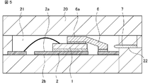
- FIG. 7 is a cross-sectional view showing a first transfer molding step of the semiconductor device according to the first embodiment of the present invention.
- FIG. 7 is a cross-sectional view showing a second transfer molding step of the semiconductor device according to the first embodiment of the present invention.
- FIG. 7 is a cross-sectional view showing a first compression molding step of the semiconductor device according to the first embodiment of the present invention. It is sectional drawing which shows the state which has arrange
- FIG. 5 is a cross-sectional view showing a semiconductor device in accordance with a second embodiment of the present invention.
- FIG. 21 is a plan view of the semiconductor device after a first transfer molding step in Embodiment 2 of the present invention as viewed from the mounting surface side.
- FIG. 21 is a plan view of the semiconductor device in which the inner leads are exposed after the first molding step in the second embodiment of the present invention, as viewed from the mounting surface side.
- FIG. 21 is a plan view of the semiconductor device after a second transfer molding step in the second embodiment of the present invention as viewed from the mounting surface side. It is sectional drawing which shows the semiconductor device concerning Embodiment 3 of this invention.
- FIG. 21 is a plan view of the semiconductor device after a first transfer molding step in Embodiment 2 of the present invention as viewed from the mounting surface side.
- FIG. 21 is a plan view of the semiconductor device in which the inner leads are exposed after the first molding step in the second embodiment of the present invention, as viewed from the mounting surface side
- FIG. 31 is a plan view of the semiconductor device after the second transfer molding step in the third embodiment of the present invention as viewed from the heat dissipation surface side. It is sectional drawing which shows the surface state of the surface roughening inner lead in Embodiment 4 of this invention. It is a top view which shows the collar-like part of the laser roughening inner lead in Embodiment 5 of this invention. It is an upper surface perspective view which shows the collar-like part of the laser roughening inner lead in Embodiment 5 of this invention. It is sectional drawing which shows the semiconductor device concerning Embodiment 6 of this invention. It is sectional drawing which shows the 2nd transfer molding process of the semiconductor device concerning Embodiment 6 of this invention.
- FIG. 1 is a cross-sectional view showing the configuration of the resin mold type semiconductor device according to the first embodiment
- FIG. 2 is a cross-sectional view showing the semiconductor device after a first transfer molding step
- FIG. FIG. 4 is a plan view of the semiconductor device after the transfer molding process as viewed from the heat dissipation surface side
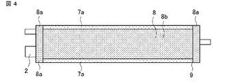
- FIG. 4 is a plan view of the semiconductor device after the second transfer molding process as viewed from the heat dissipation surface side.
- the same or corresponding parts are denoted by the same reference numerals.
- the semiconductor device 100 is a double-sided heat radiation semiconductor device sealed using two types of resins.
- the semiconductor device 100 includes a lead frame 2 on which the semiconductor element 1 is mounted, an external terminal 4, wires 5 and inner leads 6 connected to electrodes of the semiconductor element 1, and a first resin. It comprises one mold resin 7 and a second mold resin 8 which is a second resin.
- the surface of the lead frame 2 on which the semiconductor element 1 is mounted is referred to as a mounting surface 2a, and the surface opposite to the mounting surface 2a is referred to as a heat dissipation surface 2b.
- the upper surface of the lead frame 2 is the mounting surface 2a
- the lower surface is the heat dissipation surface 2b.
- a semiconductor element 1 such as, for example, an IGBT, a MOSFET, an IC chip, an LSI chip, etc. is mounted via a bonding member 3 such as solder or silver.
- the lead frame 2 is a copper plate or a copper alloy plate, and the surface thereof is coated with a metal plating (not shown) such as gold, silver, nickel, or tin.
- the electrode pad of the semiconductor element 1 is electrically connected to the external terminal 4 through the wire 5 connected by wire bonding, or the inner lead 6 made of a material of a copper plate or a copper alloy plate, and a signal is input to the outside Make an output.
- the wire 5 and the inner lead 6 can be replaced with each other.
- the wire 5 is made of gold, silver, aluminum, copper or the like, and the wire wire diameter is about 20 ⁇ m to 500 ⁇ m.
- a part of the lead frame 2, the semiconductor element 1, the wires 5 and the inner leads 6 are sealed by a first mold resin 7 and a second mold resin 8.
- Each of the first mold resin 7 and the second mold resin 8 is a thermosetting epoxy resin or the like.
- a high heat dissipation resin having a thermal conductivity higher than that of the first mold resin 7 is used for the second mold resin 8 mainly covering the heat dissipation surface 2 b.
- the thermal conductivity of the second mold resin 8 is 2 W / m ⁇ K to 12 W / m ⁇ K.
- a low stress resin which is a mold resin of a general integrated circuit is used for the first mold resin 7 mainly covering the mounting surface 2a.
- a heat dissipating surface side skirt portion which is a frame-like protrusion having a thickness of about 0.3 mm to 2 mm, which is molded by the first mold resin 7 and the second mold resin 8 is provided.
- the first thin-walled molding portion 8b covering two opposing sides of the heat dissipation surface side skirt portion and the space between the two sides is integrally molded with the second mold resin 8, and the other two opposing sides are the first It is molded by the mold resin 7.
- the heat dissipation surface side skirt portion is formed of a first skirt portion 7 a molded by the first mold resin 7 and a second skirt portion molded by the second mold resin 8. It comprises a skirt portion 8a.
- the first skirt portion 7a and the second skirt portion 8a have a rectangular, square, or trapezoidal cross-sectional shape cut in the direction orthogonal to each side.
- the corner part of the said cross-sectional shape may be rounded, or the said cross-sectional shape may be circular arc shape.
- a first thin molded portion 8b having a thickness of about 0.02 mm to 0.3 mm is integrally molded with the second skirt portion 8a by the second mold resin 8. ing.
- the first skirt 7 a and the second skirt 8 a are joined at four resin joints 9.
- an element sealing portion 7 b covering a part of the inner lead 6 and the semiconductor element 1 is molded by the first mold resin 7.
- the element sealing portion 7b has an upper surface 7c which is a flat surface parallel to the mounting surface 2a, and four side surfaces orthogonal to the upper surface 7c.
- the upper surface 7c of the element sealing portion 7b and the four side surfaces do not have to be orthogonal to each other.
- the inner lead 6 also has an end face 6a parallel to the top surface 7c of the element sealing portion 7b.
- the top surface 7c of the element sealing portion 7b and the end surface 6a of the inner lead 6 are formed to have the same height from the mounting surface 2a.
- a second thin molded portion 8 c covering a part of the surface of the element sealing portion 7 b and the inner leads 6 exposed from the element sealing portion 7 b is formed by the second mold resin 8.
- the second thin molded portion 8c covers one side surface orthogonal to the top surface 7c of the element sealing portion 7b, the end surface 6a of the inner lead 6, and the top surface 7c of the element sealing portion 7b.
- FIG. 5 shows a first transfer molding step
- FIG. 6 shows a second transfer molding step.
- the semiconductor device shown in FIG. 6 is a cross-sectional view at a position shown by AA in FIG.
- the first mold resin 7 melted by the heat and pressure applied by the first molding die 20 is installed with the lead frame 2 through the upper gate 22. It is injected into the cavity 21 that has been The first mold resin 7 flows to the mounting surface 2 a side of the lead frame 2 and fills the cavity 21 to form the element sealing portion 7 b, and a cavity (not shown) corresponding to the first skirt 7 a Flow to form the first skirt 7a.
- the end face 6 a of the inner lead 6 is covered with the first mold resin 7 after the first transfer molding step. Therefore, in a later step, the first mold resin 7 is cut by mechanical grinding or laser irradiation to expose the end face 6 a of the inner lead 6.
- the element sealing portion 7 b for sealing the semiconductor element 1 with the first mold resin 7 is molded on the mounting surface 2 a of the lead frame 2 after the first transfer molding step and the post step.
- the end face 6a of the inner lead 6 is exposed from the element sealing portion 7b.
- a first skirt portion 7 a having two sides parallel to the upper gate 22 is formed on the heat dissipation surface 2 b by the first mold resin 7.
- a second transfer molding step is carried out.
- the first mold resin 7 is subjected to UV treatment, plasma treatment or laser treatment after the first transfer molding step in order to enhance the adhesion between the first mold resin 7 and the second mold resin 8. Good.
- the lead frame 2 that has completed the first transfer molding process is installed inside the second molding die 30.
- the inside of the second molding die 30 in which the lead frame 2 is installed has a cavity 31a corresponding to the second thin-walled molding portion 8c in the upper part of the element sealing portion 7b molded by the first molding resin 7. Have. Further, on the side of the heat dissipation surface 2b of the lead frame 2, a cavity 31b corresponding to the first thin molded portion 8b and a cavity 31c corresponding to the second skirt portion 8a are provided.
- the second mold resin 8 melted by the heat and pressure applied by the second mold 30 flows through the cavity 31 c near the lower gate 32 and flows to the cavity 31 b. At this time, since the second mold resin 8 temporarily accumulates in the cavity 31 c near the lower gate 32, it can flow uniformly to the cavity 31 b.
- the second mold resin 8 having passed through the cavity 31 b further flows to the cavity 31 c on the opposite side farthest from the lower gate 32 which is to be the final filling portion. At this time, the second mold resin 8 is hardened and the viscosity is high, but the cavity 31 c which is the final filling portion is larger in thickness than the cavity 31 b and smaller in flow resistance. Flow easily.
- the second mold resin 8 flows between the upper surface 7 c of the element sealing portion 7 b molded by the first mold resin 7 and the second molding die 30 simultaneously with the flow to the cavities 31 b and 31 c. It flows to the cavity 31a.
- the thickness of the second thin molded portion 8c may be about twice as thick as that of the first thin molded portion 8b in consideration of the flowability and heat dissipation of the resin.
- the thickness of the element sealing portion 7b is at least 0.4 mm or more, and by adding the thickness of the second thin molded portion 8c to this, the insulation on the mounting surface 2a side can be ensured.
- the second skirt portion 8a, the first thin-walled molding portion 8b, and the second thin-walled molding portion 8c are molded with the second mold resin 8, and from the second molding die 30 Take out the molded article.
- the thin molded portion 8 b is integrally molded with the second mold resin 8.
- the first skirt 7a molded by the first mold resin 7 is located on the long side
- the second skirt 8a molded by the second mold resin 8 is It is located on the short side, but may be reversed depending on the position of the gate of the molding die used.
- thermoplastic fluoroplastic film 42 having a thickness of about 40 ⁇ m to 200 ⁇ m is adsorbed in advance on the inner surface of a molding die 40 for compression. The film 42 prevents the melted first mold resin 7 from intruding into the movable portion of the molding die 40.
- the upper part of the molding die 40 is a movable part, which moves in the direction of the arrow A and stops at a predetermined position on the upper surface of the inner lead 6 while pressing the cavity 41.
- Granular first mold resin 7 may be installed in advance in the cavity 41 inside the molding die 40, or a tablet resin for ordinary transfer is injected from the upper gate 22 and flows into the cavity 41. You may do it.
- the film 42 previously installed in the molding die 40 is pressed and made thinner, thereby absorbing variations in the height of the semiconductor element 1 and the inner leads 6, and Since the gap with the inner lead 6 is filled, resin burrs do not occur, and the end face 6 a of the inner lead 6 can be exposed.
- the flowability of the second mold resin 8 to the first thin-walled molding portion 8b is improved by molding the heat dissipation surface side skirt portion through two transfer molding steps, and the first molding resin is produced. 7 and the lead frame 2 are easily wetted and adhesion is improved.
- the thickness of the heat dissipating surface side skirt portion is larger than the first thin wall molded portion and the flow resistance is smaller, so the molten resin flows first to the four sides of the heat dissipating surface side skirt portion, and the first thin wall forming The part will be the final filling part.
- the resin which has been hardened and whose viscosity is increased flows in the final filling portion, and therefore, it is difficult to uniformly flow to the first thin-walled molding portion having high flow resistance.
- the resin that has flowed to the four sides of the heat dissipation surface side skirt joins first in the first thin-walled forming portion, a weld line is formed, and the case of forming by two transfer molding steps as in the first embodiment. In comparison with the above, the strength and the insulation of the first thin-walled molded portion are inferior.
- the semiconductor device 100 is used for a power conversion device including an inverter that converts power and a motor that converts electrical energy into mechanical energy.
- a power conversion device including an inverter that converts power and a motor that converts electrical energy into mechanical energy.
- it is incorporated into an inverter of a motor in which a motor and an inverter are integrated.
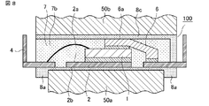
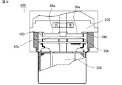
- the heat dissipation surface heat dissipation plate 50a and the mounting surface heat dissipation plate 50b are in contact with the semiconductor device 100 via a heat dissipation grease (not shown).
- the heat dissipation surface heat dissipation plate 50a is sized to fit within the frame of the heat dissipation surface side skirt portion.
- the heat dissipating surface heat dissipating plate 50a and the mounting surface heat dissipating plate 50b may be integrated with an inverter casing or motor casing having a large heat capacity, or may be joined to these casings by screwing or the like.
- Motors 400 and 401 shown in FIGS. 9 and 10 may be integrated units of a motor and an inverter for electric power steering, ISG (Integrated Starter Generator) for mild hybrid, and an integrated unit of a motor and inverter for strong hybrid.
- the motors 300 and 301 have a stator and a rotor disposed inside a metal casing, and the inverters 200 and 201 have a motor drive circuit.
- the motor 400 shown in FIG. 9 the motor 300 and the inverter 200 are integrated, and the heat dissipation surface heat dissipation plate 50 a and the mounting surface heat dissipation plate 50 b are integrated with the casing of the inverter 200.
- the motor 401 shown in FIG. 10 the motor 301 and the inverter 201 are integrated, the heat dissipation surface heat dissipation plate 50a is integrated with the housing of the motor 301, and the mounting surface heat dissipation plate 50b is integrated with the housing of the inverter 201.
- the mounting surface heat dissipation plate 50 b may be integrated with the housing of the motor 301, and the heat dissipation surface heat dissipation plate 50 a may be integrated with the housing of the inverter 201.
- the heat sink and the housing may be separate bodies, and may be contacted via heat release grease or the like to screw and fix the heat sink to the housing.
- the surface of the lead frame 2 is coated with a metal plating of gold, silver, nickel, tin or the like, but may not be coated. Moreover, although the thickness of the lead frame 2 is uniform, a partially different lead frame may be used (however, in this case, the cost is increased). Further, the surface of the inner lead 6 is not coated by metal plating, but may be coated.
- the upper surface 7 c of the element sealing portion 7 b and one side surface closest to the lower gate 32 are covered with the second mold resin 8, but the arrangement of the second mold resin 8 is It is not limited to this. Since the second mold resin 8 which is a high heat dissipation resin is expensive, the arrangement may be determined in consideration of heat dissipation and cost.
- the semiconductor device 100 according to the first embodiment is suitable as a power module having a withstand voltage of 600 V or more, which uses an IGBT as the semiconductor element 1.
- first skirt 7a is molded by the first mold resin 7, and the second skirt 8a and the first thin-walled molding 8b are integrally molded by the second mold resin 8, so that the heat is released.
- the fluidity of the second mold resin 8 is improved as compared with the case where all the four sides of the surface side skirt portion are molded with the second mold resin 8 at one time, and the lead frame 2 and the first mold resin 7 are wetted
- the adhesion is improved. Therefore, the adhesion between the first thin-walled molding portion 8b and the lead frame 2 is enhanced, and peeling and chipping of the first thin-walled molding portion 8b are unlikely to occur.
- the heat generated in the semiconductor element 1 can be efficiently obtained from both the first thin molding portion 8b and the second thin molding portion 8c. It can be released and heat dissipation improves.
- the heat dissipation property can be improved while suppressing the amount of use of the expensive high heat dissipation resin.
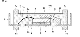
- FIG. 11 is a cross-sectional view showing the configuration of the semiconductor device according to the second embodiment of the present invention.
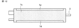
- 12 is a plan view of the semiconductor device after the first transfer molding step as viewed from the mounting surface side
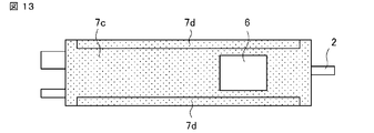
- FIG. 13 is a view from the mounting surface side of the semiconductor device where the inner leads are exposed after the first molding step.
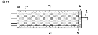
- FIG. 14 is a plan view of the semiconductor device after the second transfer molding step as viewed from the mounting surface side.
- the creeping distance can be increased at low cost by providing the frame-like projections on the mounting surface 2a side as well as the heat dissipating surface 2b side.
- a mounting surface side skirt portion which is a mounting surface side frame-like protrusion having a thickness of about 0.3 mm to 2 mm, is provided at the outer peripheral end of the upper surface 7c of the element sealing portion 7b. It is done.
- the second thin molded portion 8c covering the opposing two sides of the mounting surface side skirt portion and the space between the two sides is integrally molded by the second mold resin 8, and the other opposing two sides of the mounting surface side skirt portion are formed.
- the side is molded by the first mold resin 7.
- the other configuration is the same as that of the semiconductor device 100 according to the first embodiment, and thus the description thereof is omitted here.
- the mounting surface side skirt portion is configured of a third skirt portion 7 d molded by the first mold resin 7 and a fourth skirt portion 8 d molded by the second mold resin 8. It is done.
- the third skirt portion 7d and the fourth skirt portion 8d have a rectangular, square, or trapezoidal cross-sectional shape cut in the direction orthogonal to the respective sides.
- the corner part of the said cross-sectional shape may be rounded, or the said cross-sectional shape may be circular arc shape.
- the second thin molded portion 8c having a thickness of about 0.02 mm to 0.3 mm is integrally formed with the fourth skirt 8d by the second mold resin 8. It is molded.
- the third skirt 7 d and the fourth skirt 8 d are joined at four resin joints 9.
- the manufacturing process of the semiconductor device 101 according to the second embodiment will be described with reference to FIGS. 12 to 14.
- the semiconductor device 101 is manufactured including two molding processes, and the first transfer molding process similar to that of the first embodiment is performed.
- the internal shape of the molding die is different from that of the first embodiment.
- a third skirt 7d having two sides parallel to the upper gate 22 is formed on the upper surface 7c of the element sealing portion 7b. It is molded by the mold resin 7 of Further, on the heat radiation surface 2b, first skirt portions 7a, which are two sides parallel to the upper gate 22, are molded with the first mold resin 7 (see FIG. 3).
- the inner lead 6 is not exposed in the case where the first transfer molding process is the normal transfer molding. For this reason, it is necessary to remove the first mold resin 7 by mechanical grinding, laser irradiation or the like in a later step to expose the inner lead 6. On the other hand, in the case where the first transfer molding process is compression molding, as shown in FIG. 13, the inner lead 6 is exposed.
- a second transfer molding process similar to that of the first embodiment is carried out.
- the internal shape of the molding die is different from that of the first embodiment.
- the fourth skirt 8 d of two sides including the side closest to the lower gate 32 is provided on the upper surface 7 c of the element sealing portion 7 b;
- the second thin molded portion 8 c covering between the two sides is integrally molded by the second mold resin 8.
- a second skirt portion 8a of two sides including the side closest to the lower gate 32 and a first thin molded portion 8b covering between the two sides is a second mold resin 8 It is integrally formed by (refer FIG. 4).
- the creeping distance becomes longer than the first embodiment by providing the mounting surface side skirt portion, so that the withstand voltage is further increased.
- a semiconductor device 101 with double-sided heat radiation can be obtained.
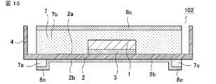
- FIG. 15 is a cross-sectional view showing the semiconductor device according to the third embodiment of the present invention
- FIG. 16 is a plan view of the semiconductor device after the second transfer molding step as viewed from the heat dissipation surface side.
- FIG. 15 is a cross-sectional view taken along the line BB in FIG.
- the heat dissipating surface side is formed by the first skirt portion 7 a molded by the first mold resin 7 and the second skirt portion 8 a molded by the second mold resin 8. I constructed a skirt.
- the heat dissipation surface heat dissipation plate 50a see FIG. 8 and the lead frame
- the creepage distance between the two is equal to the thickness of the first thin molded portion 8b, and there is a concern that the withstand voltage may be greatly reduced.
- two opposing sides of the heat dissipation surface side skirt portion molded by the first mold resin 7, that is, the first skirt portion 7a, is a second mold resin.
- a fifth skirt portion 8e formed by the step 8 is covered.
- the fifth skirt portion 8e is formed during the second transfer molding, and as shown in FIG. 15, covers the inner side surface of the first skirt portion 7a and the lower surface parallel to the heat dissipation surface 2b.
- the heat dissipation surface 2b side of the semiconductor device 102 covers the four sides (the second skirt portion 8a and the fifth skirt portion 8e) of the heat dissipation surface side skirt portion and the four sides.
- the first thin molded portion 8 b is integrally molded of the second mold resin 8.
- the height of the first skirt portion 7a is formed lower than that of the first embodiment.
- the first molding is performed by the second mold resin 8 in the second transfer molding.
- a sixth skirt may be formed to cover the third skirt 7d formed by the mold resin 7.
- the first skirt 7a is covered with the fifth skirt 8e, so that variations in production and the like cause the heat radiation surface 2b to Even if the interface between the first thin molded portion 8b and the first skirt 7a is peeled off, the creeping distance can be secured, and the semiconductor device 102 capable of reducing the insulation failure can be obtained.
- FIG. 17 is a cross-sectional view showing the surface state of the surface-roughened inner lead used in the semiconductor device according to the fourth embodiment of the present invention.
- the entire configuration and manufacturing method of the semiconductor device according to the fourth embodiment are the same as those of the first embodiment, and thus the description thereof is omitted here.
- the semiconductor device according to the fourth embodiment is a substitute for the inner lead 6 used in the first embodiment in order to improve the adhesion between the first mold resin 7 and the second mold resin 8 and the inner lead.
- the surface roughening inner lead 11 is used.
- the surface roughened inner lead 11 is obtained by chemically or physically roughening the surface of the inner lead made of copper or copper alloy to a surface roughness Ra of about 0.06 to 0.2. Since numerous bumps and dips are formed on the surface of the surface-roughened inner lead 11, a high anchoring effect can be obtained.
- the first mold resin 7 and the first mold resin 7 can be used more than in the case where the normal inner lead 6 is used.
- the adhesion to the second mold resin 8 is improved.
- the surface roughening inner lead 11 has a larger surface area than the normal inner lead 6, the heat dissipation can be improved.
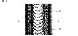
- FIG. 18 is a plan view showing a ridge portion of a laser-roughened inner lead according to a fifth embodiment of the present invention
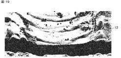
- FIG. 19 is a top perspective view of a cross section of a portion indicated by C-C in FIG.
- the entire configuration and manufacturing method of the semiconductor device according to the fifth embodiment are the same as those of the first embodiment, and thus the description thereof is omitted here.
- the semiconductor device is a substitute for the inner leads 6 used in the first embodiment in order to improve the adhesion between the first mold resin 7 and the second mold resin 8 and the inner leads.
- the laser roughened inner lead 12 is used.
- the laser roughened inner lead 12 has a ridge-like portion 13 in which the surface shape of the metal constituting the inner lead or the metal plating covering the surface of the inner lead is deformed into a wedge shape. Since the scaly portion 13 has a scaly protrusion continuously arranged and has a complicated shape in which both sides are raised high, a high anchoring effect can be obtained by disposing the scaly portion 13.
- the ridge portion 13 is formed by melting the metal or metal plating constituting the inner lead by continuously performing spot irradiation with a laser and deforming it into a ridge shape.
- the formation of the ridged portion 13 on the inner lead can be performed together, for example, when the inner lead is exposed by laser irradiation after the first transfer step.
- the ridge portion 13 is formed by laser irradiation, it is selectively applied to an arbitrary portion of the inner lead, for example, a portion where stress is applied when the semiconductor device is discharged from the molding die and initial peeling easily occurs. Can be placed.
- the width and height of the bowl-like portion 13 can be adjusted by the output of the laser, the scanning speed, and the like.
- the width of the ridge-like portion 13 is desirably 60 ⁇ m or more, and the adhesion is further improved by increasing the width according to the area of the portion to be disposed.
- the first mold resin 7 and the first mold resin 7 can be used more than in the case where the normal inner lead 6 is used.
- the adhesion to the second mold resin 8 is improved.
- the surface roughening of the laser roughened inner lead 12 is larger than that of the normal inner lead 6, the heat dissipation can be improved.
- FIG. 20 is a cross-sectional view showing a semiconductor device according to the sixth embodiment of the present invention
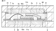
- FIG. 21 is a cross-sectional view showing a second transfer molding step of the semiconductor device according to the sixth embodiment.
- the heat dissipation surface heat dissipation plate 51a and the mounting surface heat dissipation plate 51b are respectively formed by the first thin-walled molding portion 8b and the second thin-walled molding portion 8c without the intervention of heat dissipation grease or the like. It is directly joined.
- the other configuration is the same as that of the semiconductor device 100 according to the first embodiment, and thus the description thereof is omitted here.
- the heat dissipation surface heat dissipation plate 51 a and the mounting surface heat dissipation plate 51 b are installed inside the molding die 60. Inside the molding die 60, a cavity 62b corresponding to the first thin-walled molding portion 8b is formed between the heat radiation surface 2b of the lead frame 2 and the heat radiation surface heat radiation plate 51a.
- a movable pin 61 installed inside the molding die 60 forms a cavity 62a corresponding to the second thin molded portion 8c between the element sealing portion 7b and the mounting surface heat sink 51b. There is. In addition, since the pin 61 is pulled out during molding, the second mold resin 8 flows late in the pin hole and the pin hole does not open.
- the second skirt portion 8a and the first thin molded portion 8b are formed on the heat dissipation surface 2b, and the mounting surface 2a is formed on the mounting surface 2a.
- the second thin molded portion 8c is molded.
- the second mold resin 8 before curing which has flowed into the cavity 62a and the cavity 62b becomes an adhesive, and the heat radiation surface heat dissipation plate 51a is joined to the first thin-walled molding portion 8b, and the second thin-walled molding portion 8c
- the mounting surface heat sink 51b is joined.
- the heat dissipation surface heat dissipation plate 51a and the mounting surface heat dissipation plate 51b are respectively provided to the first thin-walled molding portion 8b and the second thin-walled molding portion 8c. Because they are directly joined, the contact thermal resistance is reduced and the heat dissipation is further improved. Further, after the second transfer molding step, the step of bonding the heat sink to the first thin molded portion 8b and the second thin molded portion 8c via the heat release grease etc. can be omitted, and the heat release grease is unnecessary. Therefore, the material cost can be reduced.
- the configuration, number, and arrangement of the components of the semiconductor device according to the first to sixth embodiments are particularly limited. It is not appropriate, but is selected appropriately according to the required function.
- the present invention can freely combine each embodiment within the scope of the invention, and can suitably modify or omit each embodiment.
- SYMBOLS 1 semiconductor element 2 lead frame, 2a mounting surface, 2b heat dissipation surface, 3 joining member, 4 external terminal, 5 wire, 6 inner lead, 6a end surface, 7 first mold resin, 7a first skirt portion, 7b element Sealed part, 7c upper surface, 7d third skirt part, 8 second mold resin, 8a second skirt part, 8b first thin molded part, 8c second thin molded part, 8d fourth skirt part , 8e fifth skirt portion, 9 resin joint portion, 11 surface roughened inner lead, 12 laser roughened inner lead, 13 ridged portion, 20 first molding die, 21, 31a, 31b, 31c, 41, 62a , 62b cavity, 22 upper gate, 30 second molding die, 32 lower gate, 40, 60 molding die, 42 film, 50a, 51a Hot face heat sink 50b, 51b mounting surface heat radiating plate, 61 pin, 100, 101, 102, 103 semiconductor device, 200, 201 inverter, 300 and 301 motor, 400 and 401 electric motor
Landscapes
- Engineering & Computer Science (AREA)
- Power Engineering (AREA)
- Microelectronics & Electronic Packaging (AREA)
- Structures Or Materials For Encapsulating Or Coating Semiconductor Devices Or Solid State Devices (AREA)
- Encapsulation Of And Coatings For Semiconductor Or Solid State Devices (AREA)
- Cooling Or The Like Of Semiconductors Or Solid State Devices (AREA)
- Motor Or Generator Frames (AREA)
- Inverter Devices (AREA)
Abstract
半導体装置(100)は、リードフレーム(2)の放熱面(2b)に、枠状突起である放熱面側スカート部を設けている。これにより、少ない樹脂の増加量で沿面距離が長くなり、絶縁性が向上する。また、二回のトランスファー成形工程を経て放熱面側スカート部を成形することにより、第二のモールド樹脂(8)の流動性が向上し、第一のモールド樹脂(7)およびリードフレーム(2)に対し濡れ易くなり密着性が向上する。さらに、実装面(2a)側において、インナーリード(6)の端面(6a)を素子封止部(7b)から露出させ、第二のモールド樹脂(8)により成形された第二の薄肉成形部(8c)で覆うことにより、半導体素子(1)で発生した熱を第一の薄肉成形部(1b)と第二の薄肉成形部(8c)の両面から効率的に逃すことができるため、放熱性が向上する。
Description
本発明は、半導体装置およびこれを備えた電力変換装置に関し、特にモールド樹脂で全体を封止した両面放熱の半導体装置に関するものである。
パワー用の半導体装置は、IGBT(Insulated Gate Bipolar Transistor)、MOSFET(Metal-oxide-semiconductor field-effect transistor)、ICチップ、LSIチップ等の半導体素子を外部端子用リードフレームにダイボンドした後、半導体素子の電極と外部端子をワイヤまたはインナーリードで電気的に接続し、外部との信号の入出力を行っている。
また、樹脂モールド型の半導体装置は、モールド成形工程において、リードフレームの半導体素子が実装された側の面(実装面)とその反対側の放熱面を、モールド樹脂で封止されている。パワー用の半導体装置は、内部に高発熱素子を備えているため、モールド樹脂には高い放熱性が要求される。
従来、樹脂モールド型の半導体装置として、リードフレームの実装面側を一般的な集積回路のモールド樹脂として用いられる低応力樹脂で封止し、放熱面側を主にアルミナフィラーを使用した熱伝導率が3W/m・K以上の高放熱樹脂で封止したものがある。また、特許文献1では、モータとインバータを備えた電力変換装置において、インバータのパワーモジュールの一方の面がモータまたはインバータの金属筐体と接し、他方の面は放熱用の金属板と接しており、パワーモジュールで発生した熱を両面から逃すようにしている。
従来の半導体装置においては、リードフレームの放熱面側を高放熱樹脂で封止したものはあるが、放熱性向上の観点からは実装面側も高放熱樹脂で覆うことが望ましい。しかしながら、高放熱樹脂は高価であるため、実装面を含む全ての領域を高放熱樹脂で覆うことはコスト面から現実的ではない。
また、特許文献1では、樹脂の厚さが300μm程度の薄いパワーモジュールに、放熱用の金属板を両面から接触させており、金属板からリードフレームまでの沿面距離が短い。このため、絶縁耐圧が低いことが予想され、絶縁不良となる可能性が高い。沿面距離を長くするためには、金属板の面積を小さくするか、あるいは樹脂を厚くする必要があり、いずれにしても放熱性が低下するという課題があった。
また、樹脂全体の厚さが300μmの半導体装置の場合、例えば半導体素子が100μm、リードフレームが100μmとすると、放熱面側の樹脂の厚さは100μm未満となる。放熱性向上のためには樹脂をより薄くする必要があるが、モールド成形工程で厚さ100μm未満の薄肉成形をする場合、ボイドまたは樹脂未充填が発生しやすく不良となる課題があった。
本発明は、上記問題点に鑑み、二種類の樹脂を用いた両面放熱の半導体装置において、沿面距離を確保し、放熱性と絶縁性に優れた低コストの半導体装置を得ることを目的とする。
本発明に係る半導体装置は、半導体素子が実装されたリードフレームと、半導体素子の電極に接続されたインナーリードと、リードフレームの一部と半導体素子とインナーリードとを封止している第一の樹脂および第二の樹脂を備えている。リードフレームの半導体素子が実装された側の面を実装面、実装面と反対側の面を放熱面とするとき、放熱面の外周端部には枠状突起が設けられ、枠状突起の対向する二辺と該二辺の間を覆う第一の薄肉成形部は第二の樹脂により一体的に成形され、枠状突起の他の対向する二辺は第一の樹脂により成形されている。実装面には、インナーリードの一部と半導体素子とを覆う素子封止部が第一の樹脂により成形され、素子封止部の表面の一部と素子封止部から露出しているインナーリードとを覆う第二の薄肉成形部が第二の樹脂により成形されている。
本発明によれば、リードフレームの放熱面に枠状突起を設けることにより、少ない樹脂の増加量で沿面距離が長くなり、絶縁性が向上する。また、枠状突起の対向する二辺と第一の薄肉成形部を第二の樹脂により一体的に成形し、他の対向する二辺を第一の樹脂により成形することにより、枠状突起の四辺全てを第二の樹脂で一度に成形する場合に比べ、第一の薄肉成形部への第二の樹脂の流動性が向上し、第二の樹脂が濡れ易くなる。このため、第一の薄肉成形部とリードフレームの密着性が高く、第一の薄肉成形部の剥離や欠けが発生しにくい。さらに、インナーリードを第二の薄肉成形部で覆うことにより、半導体素子で発生した熱を第一の薄肉成形部と第二の薄肉成形部の両面から効率的に逃すことができる。これらのことから、本発明によれば、低コストで放熱性と絶縁性に優れた信頼性の高い半導体装置が得られる。
この発明の上記以外の目的、特徴、観点および効果は、図面を参照する以下のこの発明の詳細な説明から、さらに明らかになるであろう。
この発明の上記以外の目的、特徴、観点および効果は、図面を参照する以下のこの発明の詳細な説明から、さらに明らかになるであろう。
実施の形態1.
以下に、本発明の実施の形態1に係る半導体装置について、図面に基づいて説明する。図1は、本実施の形態1に係る樹脂モールド型の半導体装置の構成を示す断面図、図2は、一回目のトランスファー成形工程後の半導体装置を示す断面図、図3は、一回目のトランスファー成形工程後の半導体装置を放熱面側から見た平面図、図4は、二回目のトランスファー成形工程後の半導体装置を放熱面側から見た平面図である。なお、各図において、図中、同一または相当部分には同一符号を付している。
以下に、本発明の実施の形態1に係る半導体装置について、図面に基づいて説明する。図1は、本実施の形態1に係る樹脂モールド型の半導体装置の構成を示す断面図、図2は、一回目のトランスファー成形工程後の半導体装置を示す断面図、図3は、一回目のトランスファー成形工程後の半導体装置を放熱面側から見た平面図、図4は、二回目のトランスファー成形工程後の半導体装置を放熱面側から見た平面図である。なお、各図において、図中、同一または相当部分には同一符号を付している。
本実施の形態1に係る半導体装置100は、二種類の樹脂を用いて封止された両面放熱の半導体装置である。図1に示すように、半導体装置100は、半導体素子1が実装されたリードフレーム2、外部端子4、半導体素子1の電極に接続されたワイヤ5とインナーリード6、第一の樹脂である第一のモールド樹脂7、および第二の樹脂である第二のモールド樹脂8を含んで構成される。
以下の説明において、リードフレーム2の半導体素子1が実装された側の面を実装面2a、実装面2aと反対側の面を放熱面2bとする。図1に示す例では、リードフレーム2の上側の面が実装面2a、下側の面が放熱面2bである。実装面2aには、例えばIGBT、MOSFET、ICチップ、LSIチップ等の半導体素子1が、はんだ、銀等の接合部材3を介して実装されている。リードフレーム2は、銅板または銅合金板であり、その表面を金、銀、ニッケル、スズ等の金属めっき(図示せず)で被膜されている。
半導体素子1の電極パッドは、ワイヤボンディングで接続されたワイヤ5、または銅板や銅合金板の材料で作成されたインナーリード6を介して外部端子4と電気的に接続され、外部と信号の入出力を行う。ワイヤ5とインナーリード6は互いに置き換えが可能である。ワイヤ5は、金、銀、アルミ、銅等からなり、ワイヤ線径は20μmから500μm程度である。
リードフレーム2の一部、半導体素子1、ワイヤ5、およびインナーリード6は、第一のモールド樹脂7と第二のモールド樹脂8で封止されている。第一のモールド樹脂7と第二のモールド樹脂8は、いずれも熱硬化性のエポキシ樹脂等である。ただし、主に放熱面2bを覆う第二のモールド樹脂8には、第一のモールド樹脂7よりも熱伝導率が高い高放熱樹脂が用いられる。第二のモールド樹脂8の熱伝導率は、2W/m・K~12W/m・Kである。また、主に実装面2aを覆う第一のモールド樹脂7には、一般的な集積回路のモールド樹脂である低応力樹脂が用いられる。
放熱面2bの外周端部には、第一のモールド樹脂7と第二のモールド樹脂8により成形された厚さ0.3mm~2mm程度の枠状突起である放熱面側スカート部が設けられている。放熱面側スカート部の対向する二辺と該二辺の間を覆う第一の薄肉成形部8bは、第二のモールド樹脂8により一体的に成形され、他の対向する二辺は第一のモールド樹脂7により成形されている。
具体的には、図4に示すように、放熱面側スカート部は、第一のモールド樹脂7により成形された第一のスカート部7aと、第二のモールド樹脂8により成形された第二のスカート部8aから構成されている。なお、第一のスカート部7aおよび第二のスカート部8aは、各辺と直交する方向に切断した断面形状が、長方形または正方形または台形である。なお、上記断面形状の角部が丸みを帯びていてもよく、あるいは上記断面形状が円弧状であってもよい。
第二のスカート部8aの間には、厚さ0.02mm~0.3mm程度の第一の薄肉成形部8bが、第二のモールド樹脂8により第二のスカート部8aと一体的に成形されている。第一のスカート部7aと第二のスカート部8aは、4箇所の樹脂接合部9で接合されている。
一方、実装面2aには、インナーリード6の一部と半導体素子1を覆う素子封止部7bが第一のモールド樹脂7により成形されている。図2に示すように、素子封止部7bは、実装面2aと平行な平面である上面7cと、この上面7cと直交する四つの側面を有している。ただし、素子封止部7bの上面7cと四つの側面は、必ずしも直交していなくてもよい。また、インナーリード6は、素子封止部7bの上面7cに平行な端面6aを有している。素子封止部7bの上面7cとインナーリード6の端面6aは、実装面2aからの高さが等しく形成されている。
さらに、素子封止部7bの表面の一部と素子封止部7bから露出しているインナーリード6とを覆う第二の薄肉成形部8cが、第二のモールド樹脂8により成形されている。図1に示す例では、第二の薄肉成形部8cは、素子封止部7bの上面7c、インナーリード6の端面6a、および素子封止部7bの上面7cと直交する一つの側面を覆っている。
半導体装置100のモールド成形工程について、図5および図6を用いて説明する。半導体装置100は、二回のトランスファー成形工程を含んで製造され、図5は一回目のトランスファー成形工程、図6は二回目のトランスファー成形工程を示している。なお、図6に示す半導体装置は、図3中A-Aで示す位置における断面図である。
図5に示すように、一回目のトランスファー成形工程において、第一の成形金型20で加える熱と圧力により溶融された第一のモールド樹脂7は、上ゲート22を通ってリードフレーム2が設置された空洞21に注入される。第一のモールド樹脂7は、リードフレーム2の実装面2a側に流動し、空洞21を充填して素子封止部7bを成形すると共に、第一のスカート部7aに該当する空洞(図示せず)に流動し、第一のスカート部7aを成形する。
なお、図5に示す第一の成形金型20を用いた場合、一回目のトランスファー成形工程後、インナーリード6の端面6aは第一のモールド樹脂7で覆われている。このため、後工程で第一のモールド樹脂7を機械研削もしくはレーザー照射等で削り、インナーリード6の端面6aを露出させる。
一回目のトランスファー成形工程および後工程を終えたリードフレーム2の実装面2aには、図2に示すように、第一のモールド樹脂7により半導体素子1を封止する素子封止部7bが成形され、インナーリード6の端面6aは素子封止部7bから露出している。また、放熱面2bには、図3に示すように、第一のモールド樹脂7により、上ゲート22と平行な二辺である第一のスカート部7aが成形されている。
続いて、二回目のトランスファー成形工程が実施される。なお、第一のモールド樹脂7と第二のモールド樹脂8の密着性を高めるため、一回目のトランスファー成形工程後、第一のモールド樹脂7にUV処理またはプラズマ処理またはレーザー処理を実施してもよい。図6に示すように、第二の成形金型30の内部には、一回目のトランスファー成形工程を終えたリードフレーム2が設置される。
リードフレーム2が設置された第二の成形金型30の内部は、第一のモールド樹脂7により成形された素子封止部7bの上部に、第二の薄肉成形部8cに該当する空洞31aを有している。また、リードフレーム2の放熱面2b側に、第一の薄肉成形部8bに該当する空洞31bと、第二のスカート部8aに該当する空洞31cを有している。
第二の成形金型30で加える熱と圧力により溶融された第二のモールド樹脂8は、下ゲート32付近にある空洞31cを通り、空洞31bへ流動する。この時、第二のモールド樹脂8は、一旦、下ゲート32付近の空洞31cに溜まるため、空洞31bへ均一に流動することができる。空洞31bを通った第二のモールド樹脂8は、さらに、最終充填部となる下ゲート32から最も遠い対辺の空洞31cに流動する。この時、第二のモールド樹脂8は、硬化が進み粘度が高くなっているが、最終充填部である空洞31cは、空洞31bよりも厚みが大きく流動抵抗が小さいため、第二のモールド樹脂8が流動しやすい。
また、第二のモールド樹脂8は、空洞31b、31cへの流動と同時に、第一のモールド樹脂7により成形された素子封止部7bの上面7cと第二の成形金型30との間の空洞31aへ流動する。第二の薄肉成形部8cの厚さは、樹脂の流動性と放熱性を考慮し、第一の薄肉成形部8bより2倍程度厚くしてもよい。素子封止部7bの厚さは少なくとも0.4mm以上とし、これに第二の薄肉成形部8cの厚さが加わることにより実装面2a側の絶縁性を確保することができる。二回目のトランスファー成形工程において、第二のモールド樹脂8により第二のスカート部8a、第一の薄肉成形部8b、および第二の薄肉成形部8cを成形し、第二の成形金型30から成形品を取り出す。
図4に示すように、二回目のトランスファー成形工程後の放熱面2bには、下ゲート32に最も近い辺を含む二辺の第二のスカート部8aと、該二辺の間を覆う第一の薄肉成形部8bが、第二のモールド樹脂8により一体的に成形されている。なお、本実施の形態1では、第一のモールド樹脂7により成形された第一のスカート部7aが長辺側に位置し、第二のモールド樹脂8により成形された第二のスカート部8aが短辺側に位置しているが、使用される成形金型のゲートの位置によって逆になる場合も有る。
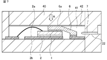
なお、一回目のトランスファー成形工程において、コンプレッション成形を実施することにより、インナーリード6の端面6aが素子封止部7bから露出した状態の成形品を製造することができる。図7に示すように、コンプレッション用の成形金型40の内部表面には、予め厚さ40μm~200μm程度の熱可塑性フッ素樹脂製のフィルム42を吸着させておく。このフィルム42は、溶融した第一のモールド樹脂7が成形金型40の可動部に侵入するのを防止する。
成形金型40の上部は可動部であり、矢印Aの方向に移動し、空洞41を加圧しながらインナーリード6上面の所定の位置で停止する。成形金型40内部の空洞41には、予め顆粒状の第一のモールド樹脂7を設置していてもよいし、通常のトランスファー用のタブレット状樹脂を上ゲート22から注入し、空洞41に流動するようにしてもよい。
図5に示す第一の成形金型20を用いてインナーリード6の端面6aを露出させるためには、第一の成形金型20とインナーリード6を接触させておく必要がある。しかし、半導体素子1およびインナーリード6の実装後の高さにはばらつきがあるため、実装後の高さが基準値よりも高い場合は半導体素子1に応力がかかり破壊される可能性があり、低い場合は第一の成形金型20とインナーリード6の間に隙間ができるため、第一のモールド樹脂7の樹脂バリが発生する。
これに対し、コンプレッション成形では、予め成形金型40内に設置されたフィルム42が加圧され薄くなることにより、半導体素子1およびインナーリード6の高さのばらつきを吸収し、成形金型40とインナーリード6との隙間を埋めるため、樹脂バリが発生せず、インナーリード6の端面6aを露出させることが可能である。
このように、二回のトランスファー成形工程を経て放熱面側スカート部を成形することにより、第二のモールド樹脂8の第一の薄肉成形部8bへの流動性が向上し、第一のモールド樹脂7およびリードフレーム2に対し濡れ易くなり、密着性が向上する。
本実施の形態1の比較例として、放熱面側スカート部の四辺全てと第一の薄肉成形部を一回のトランスファー成形工程で同時に成形した場合について説明する。成形金型内において、放熱面側スカート部の厚みは第一の薄肉成形部よりも大きく流動抵抗が小さいため、溶融樹脂は放熱面側スカート部の四辺に先に流動し、第一の薄肉成形部が最終充填部となる。
最終充填部には、硬化が進み粘度が高くなった樹脂が流動するため、流動抵抗の大きい第一の薄肉成形部へ均一に流動することが難しい。また、先に放熱面側スカート部の四辺に流動した樹脂が第一の薄肉成形部で合流するためウェルドラインが形成され、本実施の形態1のように二回のトランスファー成形工程で成形した場合に比べて第一の薄肉成形部の強度および絶縁性が劣るものとなる。
本実施の形態1に係る半導体装置100は、電力を変換するインバータ、および電気エネルギーを機械エネルギーへ変換するモータを備えた電力変換装置に用いられる。例えば車載用途においてモータとインバータが一体となった電動機のインバータに組込まれる。その際、半導体装置100には、図8に示すように、放熱面放熱板50aと実装面放熱板50bが放熱グリース(図示せず)を介して接触する。放熱面放熱板50aは、放熱面側スカート部の枠内に収まる大きさとする。放熱面放熱板50aと実装面放熱板50bは、熱容量が大きいインバータの筐体またはモータの筐体と一体化されるか、あるいはそれらの筐体にねじ締め等で接合される。
図9および図10は、本実施の形態1に係る半導体装置100を備えた電動機を示している。図9および図10に示す電動機400、401は、電動パワーステアリング用モータとインバータの統合ユニット、マイルドハイブリッド用ISG(Integrated Starter Generator)、ストロングハイブリッド用モータとインバータの統合ユニットのいずれであってもよい。モータ300、301は、金属筐体の内部に配置された固定子と回転子を有し、インバータ200、201はモータ駆動回路を有している。
図9に示す電動機400は、モータ300とインバータ200が一体化され、放熱面放熱板50aと実装面放熱板50bはインバータ200の筐体と一体化されている。また、図10に示す電動機401は、モータ301とインバータ201が一体化され、放熱面放熱板50aはモータ301の筐体と、実装面放熱板50bはインバータ201の筐体とそれぞれ一体化されている。なお、図10に示す例とは逆に、実装面放熱板50bがモータ301の筐体と一体化され、放熱面放熱板50aがインバータ201の筐体と一体化されていてもよい。また、放熱板と筐体は別体でもよく、放熱グリース等を介して接触させ、放熱板を筐体へねじ締め固定してもよい。
本実施の形態1では、リードフレーム2の表面は、金、銀、ニッケル、スズ等の金属めっきで被膜されているが、被膜されていない場合もある。また、リードフレーム2の厚さは均一であるが、部分的に厚さが異なるリードフレームを用いてもよい(ただしその場合、コストが高くなる)。また、インナーリード6の表面は金属めっきで被膜されていないが、被膜されていてもよい。
また、本実施の形態1では、素子封止部7bの上面7cと下ゲート32に最も近い一つの側面を第二のモールド樹脂8で覆うようにしたが、第二のモールド樹脂8の配置はこれに限定されるものではない。高放熱樹脂である第二のモールド樹脂8は高価であるため、放熱性とコスト面を考慮して配置を決定すればよい。
本実施の形態1によれば、リードフレーム2の放熱面2bに放熱面側スカート部を設けることにより、樹脂成形の高圧がかかるリードフレーム2の外周端部の強度を確保することができると共に、少ない樹脂の増加量で沿面距離が長くなり、絶縁性が向上する。このため、本実施の形態1に係る半導体装置100は、半導体素子1としてIGBTを使用する耐電圧600V以上のパワーモジュールとして好適である。
また、第一のスカート部7aを第一のモールド樹脂7により成形し、第二のスカート部8aと第一の薄肉成形部8bを第二のモールド樹脂8により一体的に成形することにより、放熱面側スカート部の四辺全てを第二のモールド樹脂8で一度に成形する場合に比べ、第二のモールド樹脂8の流動性が向上し、リードフレーム2および第一のモールド樹脂7に対して濡れ易くなり密着性が向上する。このため、第一の薄肉成形部8bとリードフレーム2との密着性が高くなり、第一の薄肉成形部8bの剥離や欠けが発生しにくい。
さらに、インナーリード6の端面6aを第二の薄肉成形部8cで覆うことにより、半導体素子1で発生した熱を第一の薄肉成形部8bと第二の薄肉成形部8cの両面から効率的に逃すことができ、放熱性が向上する。また、実装面2a側は、第二の薄肉成形部8cのみを第二のモールド樹脂8で成形するようにしたので、高価な高放熱樹脂の使用量を抑制しつつ、放熱性を向上することができる。これらのことから、本実施の形態1によれば、低コストで放熱性と絶縁性に優れた信頼性の高い半導体装置100が得られる。
実施の形態2.
図11は、本発明の実施の形態2に係る半導体装置の構成を示す断面図である。また、図12は、一回目のトランスファー成形工程後の半導体装置を実装面側から見た平面図、図13は、一回目の成形工程後、インナーリードを露出させた半導体装置を実装面側から見た平面図、図14は、二回目のトランスファー成形工程後の半導体装置を実装面側から見た平面図である。
図11は、本発明の実施の形態2に係る半導体装置の構成を示す断面図である。また、図12は、一回目のトランスファー成形工程後の半導体装置を実装面側から見た平面図、図13は、一回目の成形工程後、インナーリードを露出させた半導体装置を実装面側から見た平面図、図14は、二回目のトランスファー成形工程後の半導体装置を実装面側から見た平面図である。
例えばストロングハイブリッド用IGBTを搭載した600V以上の耐電圧が必要な半導体装置の場合、沿面距離を通常よりも長く(例えば1.8mm以上)確保する必要がある。素子封止部7bを厚くすることにより沿面距離は長くなるが、モジュールが大型となり樹脂の使用量が増えコストが増加する。このような課題に対し、放熱面2b側と同様に実装面2a側にも枠状突起を設けることにより、低コストで沿面距離を長くすることができる。
本実施の形態2に係る半導体装置101は、素子封止部7bの上面7cの外周端部に、厚さ0.3mm~2mm程度の実装面側枠状突起である実装面側スカート部が設けられている。実装面側スカート部の対向する二辺と該二辺の間を覆う第二の薄肉成形部8cは第二のモールド樹脂8により一体的に成形され、実装面側スカート部の他の対向する二辺は第一のモールド樹脂7により成形されている。それ以外の構成については上記実施の形態1に係る半導体装置100と同様であるので、ここでは説明を省略する。
図14に示すように、実装面側スカート部は、第一のモールド樹脂7により成形された第三のスカート部7dと、第二のモールド樹脂8により成形された第四のスカート部8dから構成されている。第三のスカート部7dおよび第四のスカート部8dは、その各辺と直交する方向に切断した断面形状が、長方形または正方形または台形である。なお、上記断面形状の角部が丸みを帯びていてもよく、あるいは上記断面形状が円弧状であってもよい。
また、第四のスカート部8dの間には、厚さ0.02mm~0.3mm程度の第二の薄肉成形部8cが、第二のモールド樹脂8により第四のスカート部8dと一体的に成形されている。第三のスカート部7dと第四のスカート部8dは、4箇所の樹脂接合部9で接合されている。
本実施の形態2に係る半導体装置101の製造工程について、図12から図14を用いて説明する。半導体装置101は、二回のモールド成形工程を含んで製造され、一回目は上記実施の形態1と同様のトランスファー成形工程を実施する。ただし、成形金型の内部形状は上記実施の形態1とは異なっている。
図12に示すように、一回目のトランスファー成形工程後の実装面2aには、素子封止部7bの上面7cに上ゲート22と平行な二辺である第三のスカート部7dが、第一のモールド樹脂7により成形されている。また、放熱面2bには、上ゲート22と平行な二辺である第一のスカート部7aが、第一のモールド樹脂7により成形されている(図3参照)。
上記実施の形態1で説明したように、一回目のトランスファー成形工程が通常のトランスファー成形の場合の成形品は、図12に示すようにインナーリード6は露出していない。このため、後工程で第一のモールド樹脂7を機械研削もしくはレーザー照射等で削り、インナーリード6を露出させる必要がある。一方、一回目のトランスファー成形工程がコンプレッション成形の場合の成形品は、図13に示すようにインナーリード6が露出している。
続いて、上記実施の形態1と同様の二回目のトランスファー成形工程を実施する。ただし、成形金型の内部形状は上記実施の形態1とは異なっている。図14に示すように、二回目のトランスファー成形後の実装面2aには、素子封止部7bの上面7cに、下ゲート32に最も近い辺を含む二辺の第四のスカート部8dと、該二辺の間を覆う第二の薄肉成形部8cが、第二のモールド樹脂8により一体的に成形されている。また、放熱面2bには、下ゲート32に最も近い辺を含む二辺の第二のスカート部8aと、該二辺の間を覆う第一の薄肉成形部8bが、第二のモールド樹脂8により一体的に成形されている(図4参照)。
本実施の形態2によれば、上記実施の形態1と同様の効果に加え、実装面側スカート部を設けることにより、上記実施の形態1よりも沿面距離が長くなるため、耐電圧がさらに高い両面放熱の半導体装置101が得られる。
実施の形態3.
図15は、本発明の実施の形態3に係る半導体装置を示す断面図、図16は、二回目のトランスファー成形工程後の半導体装置を放熱面側から見た平面図である。なお、図15は、図16中B-Bで示す位置における断面図である。
図15は、本発明の実施の形態3に係る半導体装置を示す断面図、図16は、二回目のトランスファー成形工程後の半導体装置を放熱面側から見た平面図である。なお、図15は、図16中B-Bで示す位置における断面図である。
上記実施の形態1および実施の形態2では、第一のモールド樹脂7により成形された第一のスカート部7aと、第二のモールド樹脂8により成形された第二のスカート部8aで放熱面側スカート部を構成した。このような構成では、第二のモールド樹脂8により成形された第一の薄肉成形部8bと第一のスカート部7aの界面が剥離した場合、放熱面放熱板50a(図8参照)とリードフレーム2間の沿面距離は第一の薄肉成形部8bの厚さと同等となり、耐電圧が大きく低下する懸念がある。
このため、本実施の形態3に係る半導体装置102は、第一のモールド樹脂7により成形された放熱面側スカート部の対向する二辺、すなわち第一のスカート部7aを、第二のモールド樹脂8により成形された第五のスカート部8eで覆うようにしたものである。第五のスカート部8eは、二回目のトランスファー成形時に成形され、図15に示すように、第一のスカート部7aの内側の側面と、放熱面2bと平行な下面を覆っている。
これにより、半導体装置102の放熱面2b側は、図16に示すように、放熱面側スカート部の四辺(第二のスカート部8a、第五のスカート部8e)と、該四辺の間を覆う第一の薄肉成形部8bが、第二のモールド樹脂8により一体的に成形されている。なお、第二のスカート部8aと第五のスカート部8eの高さを揃えるため、第一のスカート部7aの高さは上記実施の形態1と比べて低く形成されている。
また、上記実施の形態2に係る半導体装置101のように、実装面側スカート部を備えている場合(図14参照)、二回目のトランスファー成形時に、第二のモールド樹脂8により、第一のモールド樹脂7により成形された第三のスカート部7dを覆う第六のスカート部(図示せず)を成形するようにしてもよい。
本実施の形態3によれば、上記実施の形態1と同様の効果に加え、第一のスカート部7aを第五のスカート部8eで覆うことにより、生産のばらつき等により放熱面2b側の第一の薄肉成形部8bと第一のスカート部7aの界面が剥離したとしても、沿面距離を確保することができ、絶縁不良を削減することが可能な半導体装置102が得られる。
実施の形態4.
図17は、本発明の実施の形態4に係る半導体装置に用いられる表面粗化インナーリードの表面状態を示す断面図である。なお、本実施の形態4に係る半導体装置の全体構成および製造方法は、上記実施の形態1と同様であるので、ここでは説明を省略する。
図17は、本発明の実施の形態4に係る半導体装置に用いられる表面粗化インナーリードの表面状態を示す断面図である。なお、本実施の形態4に係る半導体装置の全体構成および製造方法は、上記実施の形態1と同様であるので、ここでは説明を省略する。
本実施の形態4に係る半導体装置は、第一のモールド樹脂7および第二のモールド樹脂8とインナーリードとの密着力の向上を図るため、上記実施の形態1で用いたインナーリード6の代わりに、表面粗化インナーリード11を用いたものである。表面粗化インナーリード11とは、銅または銅合金製のインナーリードの表面を、表面粗さRa0.06~0.2程度に化学的、もしくは物理的に粗化させたものである。表面粗化インナーリード11の表面には、無数の凹凸が形成されているため、高いアンカー効果が得られる。
本実施の形態4によれば、上記実施の形態1と同様の効果に加え、表面粗化インナーリード11を用いることにより、通常のインナーリード6を用いた場合よりも第一のモールド樹脂7および第二のモールド樹脂8との密着力が向上する。さらに、表面粗化インナーリード11は、通常のインナーリード6に比べ表面積が大きいため、放熱性の向上が図られる。
実施の形態5.
図18は、本発明の実施の形態5におけるレーザー粗化インナーリードの鱗状部を示す平面図、図19は、図18中、C-Cで示す部分の断面の上面斜視図である。なお、本実施の形態5に係る半導体装置の全体構成および製造方法は、上記実施の形態1と同様であるので、ここでは説明を省略する。
図18は、本発明の実施の形態5におけるレーザー粗化インナーリードの鱗状部を示す平面図、図19は、図18中、C-Cで示す部分の断面の上面斜視図である。なお、本実施の形態5に係る半導体装置の全体構成および製造方法は、上記実施の形態1と同様であるので、ここでは説明を省略する。
本実施の形態5に係る半導体装置は、第一のモールド樹脂7および第二のモールド樹脂8とインナーリードとの密着力の向上を図るため、上記実施の形態1で用いたインナーリード6の代わりに、レーザー粗化インナーリード12を用いたものである。レーザー粗化インナーリード12は、インナーリードを構成する金属またはインナーリードの表面を被覆する金属めっきの表面形状を鱗状に変形させた鱗状部13を有している。鱗状部13は、鱗片状の突起が連続的に配置され、その両側が高く盛り上がった複雑な形状であるため、鱗状部13を配置することにより高いアンカー効果が得られる。
鱗状部13は、レーザーによるスポット照射を連続的に行うことにより、インナーリードを構成する金属または金属めっきを溶融させ、鱗状に変形させることにより形成される。インナーリードに対する鱗状部13の形成は、例えば一回目のトランスファー工程後、レーザー照射でインナーリードを露出させる際に併せて行うことができる。
また、鱗状部13は、レーザー照射により形成されるため、インナーリードの任意の箇所、例えば半導体装置を成形金型から排出する際に応力がかかり初期的な剥離が生じやすい箇所等に、選択的に配置することができる。鱗状部13の幅や高さは、レーザーの出力や走査スピード等により調整することができる。鱗状部13の幅は60μm以上が望ましく、配置される箇所の面積に応じて幅を大きくすることにより、密着性がさらに向上する。
本実施の形態5によれば、上記実施の形態1と同様の効果に加え、レーザー粗化インナーリード12を用いることにより、通常のインナーリード6を用いた場合よりも第一のモールド樹脂7および第二のモールド樹脂8との密着力が向上する。また、レーザー粗化インナーリード12は、通常のインナーリード6に比べ表面積が大きいため、放熱性の向上が図られる。
実施の形態6.
図20は、本発明の実施の形態6に係る半導体装置を示す断面図、図21は、本実施の形態6に係る半導体装置の二回目のトランスファー成形工程を示す断面図である。本実施の形態6に係る半導体装置103は、放熱面放熱板51aおよび実装面放熱板51bが、放熱グリース等を介さずに、それぞれ第一の薄肉成形部8b、第二の薄肉成形部8cと直に接合されたものである。それ以外の構成については上記実施の形態1に係る半導体装置100と同様であるので、ここでは説明を省略する。
図20は、本発明の実施の形態6に係る半導体装置を示す断面図、図21は、本実施の形態6に係る半導体装置の二回目のトランスファー成形工程を示す断面図である。本実施の形態6に係る半導体装置103は、放熱面放熱板51aおよび実装面放熱板51bが、放熱グリース等を介さずに、それぞれ第一の薄肉成形部8b、第二の薄肉成形部8cと直に接合されたものである。それ以外の構成については上記実施の形態1に係る半導体装置100と同様であるので、ここでは説明を省略する。
本実施の形態6では、図21に示すように、二回目のトランスファー成形工程において、成形金型60の内部に放熱面放熱板51aおよび実装面放熱板51bが設置される。成形金型60の内部において、リードフレーム2の放熱面2bと放熱面放熱板51aとの間には、第一の薄肉成形部8bに該当する空洞62bが形成されている。
また、成形金型60の内部に設置された可動なピン61により、素子封止部7bと実装面放熱板51bとの間に、第二の薄肉成形部8cに該当する空洞62aが形成されている。なお、ピン61は成形中に引き抜かれるため、ピン穴に第二のモールド樹脂8が遅れて流動し、ピン穴が開くことはない。
上記実施の形態1と同様に、二回目のトランスファー成形工程において、第二のモールド樹脂8により、放熱面2bに第二のスカート部8aと第一の薄肉成形部8bを、実装面2aに第二の薄肉成形部8cを成形する。この時、空洞62a、空洞62bへ流動した硬化前の第二のモールド樹脂8が接着剤となり、第一の薄肉成形部8bに放熱面放熱板51aが接合され、第二の薄肉成形部8cに実装面放熱板51bが接合される。
本実施の形態6によれば、上記実施の形態1と同様の効果に加え、第一の薄肉成形部8bおよび第二の薄肉成形部8cに、それぞれ放熱面放熱板51aと実装面放熱板51bが直接接合されるため、接触熱抵抗が低下し、放熱性がさらに向上する。また、二回目のトランスファー成形工程後、第一の薄肉成形部8bおよび第二の薄肉成形部8cに放熱グリース等を介して放熱板を接合する工程を省略することができると共に、放熱グリースが不要となるため材料コストの低減が図られる。
なお、上記実施の形態1から実施の形態6に係る半導体装置の各構成要素、例えば半導体素子1、外部端子4、ワイヤ5、およびインナーリード6等の形状、個数、および配置は、特に限定されるものではなく、求められる機能に応じて適宜選択される。本発明は、その発明の範囲内において、各実施の形態を自由に組み合わせたり、各実施の形態を適宜、変形、省略することが可能である。
1 半導体素子、2 リードフレーム、2a 実装面、2b 放熱面、3 接合部材、4 外部端子、5 ワイヤ、6 インナーリード、6a 端面、7 第一のモールド樹脂、7a 第一のスカート部、7b 素子封止部、7c 上面、7d 第三のスカート部、8 第二のモールド樹脂、8a 第二のスカート部、8b 第一の薄肉成形部、8c 第二の薄肉成形部、8d 第四のスカート部、8e 第五のスカート部、9 樹脂接合部、11 表面粗化インナーリード、12 レーザー粗化インナーリード、13 鱗状部、20 第一の成形金型、21、31a、31b、31c、41、62a、62b 空洞、22 上ゲート、30 第二の成形金型、32 下ゲート、40、60 成形金型、42 フィルム、50a、51a 放熱面放熱板、50b、51b 実装面放熱板、61 ピン、100、101、102、103 半導体装置、200、201 インバータ、300、301 モータ、400、401 電動機
Claims (12)
- 半導体素子が実装されたリードフレーム、前記半導体素子の電極に接続されたインナーリード、前記リードフレームの一部と前記半導体素子と前記インナーリードとを封止している第一の樹脂および第二の樹脂を備えた半導体装置であって、
前記リードフレームの前記半導体素子が実装された側の面を実装面、前記実装面と反対側の面を放熱面とするとき、
前記放熱面の外周端部には枠状突起が設けられ、前記枠状突起の対向する二辺と該二辺の間を覆う第一の薄肉成形部は前記第二の樹脂により一体的に成形され、前記枠状突起の他の対向する二辺は前記第一の樹脂により成形されており、
前記実装面には、前記インナーリードの一部と前記半導体素子とを覆う素子封止部が前記第一の樹脂により成形され、前記素子封止部の表面の一部と前記素子封止部から露出している前記インナーリードとを覆う第二の薄肉成形部が前記第二の樹脂により成形されていることを特徴とする半導体装置。 - 前記第一の樹脂により成形されている前記枠状突起の二辺は、前記第二の樹脂で覆われていることを特徴とする請求項1記載の半導体装置。
- 前記素子封止部は前記実装面と平行な平面を有し、前記平面の外周端部に実装面側枠状突起が設けられ、前記実装面側枠状突起の対向する二辺と該二辺の間を覆う前記第二の薄肉成形部は前記第二の樹脂により一体的に成形され、前記実装面側枠状突起の他の対向する二辺は前記第一の樹脂により成形されていることを特徴とする請求項1または請求項2に記載の半導体装置。
- 前記第一の樹脂により成形されている前記実装面側枠状突起の二辺は、前記第二の樹脂で覆われていることを特徴とする請求項3記載の半導体装置。
- 前記素子封止部は前記実装面と平行な平面を有すると共に、前記インナーリードは前記平面に平行な端面を有しており、前記平面と前記端面は、前記実装面からの高さが等しいことを特徴とする請求項1から請求項4のいずれか一項に記載の半導体装置。
- 前記第二の薄肉成形部は、前記素子封止部の前記平面および前記平面から露出している前記インナーリードの前記端面を覆っていることを特徴とする請求項5記載の半導体装置。
- 前記インナーリードは、表面が粗化されていることを特徴とする請求項1から請求項6のいずれか一項に記載の半導体装置。
- 前記インナーリードは、鱗片状の突起が連続的に配置された鱗状部を有することを特徴とする請求項1から請求項6のいずれか一項に記載の半導体装置。
- 前記第二の樹脂は、前記第一の樹脂よりも熱伝導率が高い高放熱樹脂であることを特徴とする請求項1から請求項8のいずれか一項に記載の半導体装置。
- 前記第一の薄肉成形部および前記第二の薄肉成形部と直に接合されている放熱板を備えたことを特徴とする請求項1から請求項9のいずれか一項に記載の半導体装置。
- 請求項1から請求項9のいずれか一項に記載の半導体装置を1つ以上備えたインバータと、モータとを含む電力変換装置であって、
前記半導体装置の前記第一の薄肉成形部および前記第二の薄肉成形部に放熱板が配置され、各々の前記放熱板は、前記インバータまたは前記モータの筐体の一部であることを特徴とする電力変換装置。 - 請求項1から請求項9のいずれか一項に記載の半導体装置を1つ以上備えたインバータと、モータとを含む電力変換装置であって、
前記半導体装置の前記第一の薄肉成形部および前記第二の薄肉成形部に放熱板が配置され、各々の前記放熱板は、前記インバータまたは前記モータの筐体に接合されていることを特徴とする電力変換装置。
Priority Applications (5)
| Application Number | Priority Date | Filing Date | Title |
|---|---|---|---|
| US16/617,233 US11302597B2 (en) | 2017-09-21 | 2017-09-21 | Semiconductor device, and power conversion device including the semiconductor device |
| PCT/JP2017/034019 WO2019058473A1 (ja) | 2017-09-21 | 2017-09-21 | 半導体装置およびこれを備えた電力変換装置 |
| JP2019542882A JP6877561B2 (ja) | 2017-09-21 | 2017-09-21 | 半導体装置およびこれを備えた電力変換装置 |
| CN201780094899.XA CN111095537B (zh) | 2017-09-21 | 2017-09-21 | 半导体装置及具备该半导体装置的功率转换装置 |
| EP17925881.9A EP3686925B1 (en) | 2017-09-21 | 2017-09-21 | Semiconductor device and power conversion device provided with same |
Applications Claiming Priority (1)
| Application Number | Priority Date | Filing Date | Title |
|---|---|---|---|
| PCT/JP2017/034019 WO2019058473A1 (ja) | 2017-09-21 | 2017-09-21 | 半導体装置およびこれを備えた電力変換装置 |
Publications (1)
| Publication Number | Publication Date |
|---|---|
| WO2019058473A1 true WO2019058473A1 (ja) | 2019-03-28 |
Family
ID=65810160
Family Applications (1)
| Application Number | Title | Priority Date | Filing Date |
|---|---|---|---|
| PCT/JP2017/034019 Ceased WO2019058473A1 (ja) | 2017-09-21 | 2017-09-21 | 半導体装置およびこれを備えた電力変換装置 |
Country Status (5)
| Country | Link |
|---|---|
| US (1) | US11302597B2 (ja) |
| EP (1) | EP3686925B1 (ja) |
| JP (1) | JP6877561B2 (ja) |
| CN (1) | CN111095537B (ja) |
| WO (1) | WO2019058473A1 (ja) |
Cited By (2)
| Publication number | Priority date | Publication date | Assignee | Title |
|---|---|---|---|---|
| JPWO2021132174A1 (ja) * | 2019-12-23 | 2021-07-01 | ||
| WO2022196453A1 (ja) * | 2021-03-18 | 2022-09-22 | 株式会社デンソー | 半導体モジュール、および、これを用いた電子装置 |
Families Citing this family (4)
| Publication number | Priority date | Publication date | Assignee | Title |
|---|---|---|---|---|
| WO2019140658A1 (zh) * | 2018-01-19 | 2019-07-25 | 深圳市大疆创新科技有限公司 | 散热结构、散热方法及装置、无人机、可读存储介质 |
| EP3848961B1 (en) * | 2018-09-06 | 2024-09-18 | Mitsubishi Electric Corporation | Semiconductor device |
| WO2021199635A1 (ja) * | 2020-03-30 | 2021-10-07 | ローム株式会社 | 半導体装置 |
| CN114391305B (zh) * | 2021-05-06 | 2023-06-13 | 英诺赛科(苏州)科技有限公司 | 氮化物基半导体模块及其制造方法 |
Citations (3)
| Publication number | Priority date | Publication date | Assignee | Title |
|---|---|---|---|---|
| JP2015201625A (ja) * | 2014-03-31 | 2015-11-12 | 株式会社東芝 | 半導体モジュール及び半導体モジュールの製造方法 |
| JP5946962B2 (ja) | 2013-05-21 | 2016-07-06 | 日立オートモティブシステムズ株式会社 | 電力変換装置 |
| WO2016166834A1 (ja) * | 2015-04-15 | 2016-10-20 | 三菱電機株式会社 | 半導体装置 |
Family Cites Families (12)
| Publication number | Priority date | Publication date | Assignee | Title |
|---|---|---|---|---|
| JPS5946962B2 (ja) * | 1981-06-11 | 1984-11-16 | 徳山積水工業株式会社 | 塩素化塩化ビニル樹脂の製造方法 |
| US5041902A (en) * | 1989-12-14 | 1991-08-20 | Motorola, Inc. | Molded electronic package with compression structures |
| JP3516789B2 (ja) * | 1995-11-15 | 2004-04-05 | 三菱電機株式会社 | 半導体パワーモジュール |
| JP5415823B2 (ja) * | 2008-05-16 | 2014-02-12 | 株式会社デンソー | 電子回路装置及びその製造方法 |
| US9093434B2 (en) * | 2011-04-04 | 2015-07-28 | Rohm Co., Ltd. | Semiconductor device and method for manufacturing semiconductor device |
| JP6028592B2 (ja) * | 2013-01-25 | 2016-11-16 | 三菱電機株式会社 | 半導体装置 |
| US9640460B2 (en) * | 2013-02-05 | 2017-05-02 | Panasonic Intellectual Property Management Co., Ltd. | Semiconductor device with a heat-dissipating plate |
| DE102013220880B4 (de) * | 2013-10-15 | 2016-08-18 | Infineon Technologies Ag | Elektronisches Halbleitergehäuse mit einer elektrisch isolierenden, thermischen Schnittstellenstruktur auf einer Diskontinuität einer Verkapselungsstruktur sowie ein Herstellungsverfahren dafür und eine elektronische Anordung dies aufweisend |
| KR20150048459A (ko) | 2013-10-28 | 2015-05-07 | 삼성전기주식회사 | 전력 모듈 패키지 |
| JP6332439B2 (ja) * | 2014-03-31 | 2018-05-30 | 富士電機株式会社 | 電力変換装置 |
| KR20160038440A (ko) | 2014-09-30 | 2016-04-07 | 삼성전기주식회사 | 전력 모듈 패키지와 이의 제작방법 |
| EP3929974A1 (en) | 2015-04-15 | 2021-12-29 | Mitsubishi Electric Corporation | Semiconductor device |
-
2017
- 2017-09-21 EP EP17925881.9A patent/EP3686925B1/en active Active
- 2017-09-21 US US16/617,233 patent/US11302597B2/en active Active
- 2017-09-21 WO PCT/JP2017/034019 patent/WO2019058473A1/ja not_active Ceased
- 2017-09-21 CN CN201780094899.XA patent/CN111095537B/zh active Active
- 2017-09-21 JP JP2019542882A patent/JP6877561B2/ja active Active
Patent Citations (3)
| Publication number | Priority date | Publication date | Assignee | Title |
|---|---|---|---|---|
| JP5946962B2 (ja) | 2013-05-21 | 2016-07-06 | 日立オートモティブシステムズ株式会社 | 電力変換装置 |
| JP2015201625A (ja) * | 2014-03-31 | 2015-11-12 | 株式会社東芝 | 半導体モジュール及び半導体モジュールの製造方法 |
| WO2016166834A1 (ja) * | 2015-04-15 | 2016-10-20 | 三菱電機株式会社 | 半導体装置 |
Non-Patent Citations (1)
| Title |
|---|
| See also references of EP3686925A4 |
Cited By (7)
| Publication number | Priority date | Publication date | Assignee | Title |
|---|---|---|---|---|
| JPWO2021132174A1 (ja) * | 2019-12-23 | 2021-07-01 | ||
| CN114868327A (zh) * | 2019-12-23 | 2022-08-05 | 三菱电机株式会社 | 电力转换装置 |
| JP7301164B2 (ja) | 2019-12-23 | 2023-06-30 | 三菱電機株式会社 | 電力変換装置 |
| CN114868327B (zh) * | 2019-12-23 | 2025-09-26 | 三菱电机株式会社 | 电力转换装置 |
| WO2022196453A1 (ja) * | 2021-03-18 | 2022-09-22 | 株式会社デンソー | 半導体モジュール、および、これを用いた電子装置 |
| JP2022144247A (ja) * | 2021-03-18 | 2022-10-03 | 株式会社デンソー | 半導体モジュール、および、これを用いた電子装置 |
| JP7608901B2 (ja) | 2021-03-18 | 2025-01-07 | 株式会社デンソー | 半導体モジュール、および、これを用いた電子装置 |
Also Published As
| Publication number | Publication date |
|---|---|
| JP6877561B2 (ja) | 2021-05-26 |
| CN111095537A (zh) | 2020-05-01 |
| US11302597B2 (en) | 2022-04-12 |
| JPWO2019058473A1 (ja) | 2020-03-26 |
| EP3686925B1 (en) | 2021-08-04 |
| CN111095537B (zh) | 2024-03-29 |
| EP3686925A4 (en) | 2020-07-29 |
| EP3686925A1 (en) | 2020-07-29 |
| US20210125891A1 (en) | 2021-04-29 |
Similar Documents
| Publication | Publication Date | Title |
|---|---|---|
| JP6877561B2 (ja) | 半導体装置およびこれを備えた電力変換装置 | |
| CN101626001B (zh) | 半导体装置及其制造方法 | |
| US9236324B2 (en) | Electric power semiconductor device and method for producing same | |
| TWI404177B (zh) | 功率半導體電路裝置及其製造方法 | |
| JP6266168B2 (ja) | 半導体装置 | |
| WO2020050325A1 (ja) | パワー半導体装置およびその製造方法、ならびに電力変換装置 | |
| JP7491707B2 (ja) | 電気回路体、電力変換装置、および電気回路体の製造方法 | |
| US9754855B2 (en) | Semiconductor module having an embedded metal heat dissipation plate | |
| JP6345342B2 (ja) | 半導体装置 | |
| JP4254527B2 (ja) | 半導体装置 | |
| JP2003007966A (ja) | 半導体装置 | |
| JP7555257B2 (ja) | 電気回路体、電力変換装置、および電気回路体の製造方法 | |
| JPWO2014122908A1 (ja) | 半導体装置およびその製造方法 | |
| JP5895220B2 (ja) | 半導体装置の製造方法 | |
| JP6575739B1 (ja) | 半導体装置、半導体装置の製造方法および電力変換装置 | |
| US10777476B2 (en) | Semiconductor device | |
| JP6797002B2 (ja) | 半導体装置および半導体装置の製造方法 | |
| JP2005116875A (ja) | 半導体装置 | |
| JP2024072609A (ja) | 電気回路体および電力変換装置 | |
| JP4258391B2 (ja) | 半導体装置 | |
| KR20180002419A (ko) | 파워 모듈 및 그 제조 방법 | |
| JP2003218291A (ja) | 半導体装置およびその製造方法 | |
| JP2009277959A (ja) | 半導体装置及びその製造方法 | |
| JP7422945B2 (ja) | 電力用半導体装置 | |
| JP2008041755A (ja) | 絶縁型大電力用半導体装置の製造方法 |
Legal Events
| Date | Code | Title | Description |
|---|---|---|---|
| 121 | Ep: the epo has been informed by wipo that ep was designated in this application |
Ref document number: 17925881 Country of ref document: EP Kind code of ref document: A1 |
|
| ENP | Entry into the national phase |
Ref document number: 2019542882 Country of ref document: JP Kind code of ref document: A |
|
| NENP | Non-entry into the national phase |
Ref country code: DE |
|
| ENP | Entry into the national phase |
Ref document number: 2017925881 Country of ref document: EP Effective date: 20200421 |