WO2019059546A1 - 탈부착 패턴을 가진 디스플레이 장치 - Google Patents
탈부착 패턴을 가진 디스플레이 장치 Download PDFInfo
- Publication number
- WO2019059546A1 WO2019059546A1 PCT/KR2018/009859 KR2018009859W WO2019059546A1 WO 2019059546 A1 WO2019059546 A1 WO 2019059546A1 KR 2018009859 W KR2018009859 W KR 2018009859W WO 2019059546 A1 WO2019059546 A1 WO 2019059546A1
- Authority
- WO
- WIPO (PCT)
- Prior art keywords
- layer
- pattern
- display device
- detachment
- touch screen
- Prior art date
- Legal status (The legal status is an assumption and is not a legal conclusion. Google has not performed a legal analysis and makes no representation as to the accuracy of the status listed.)
- Ceased
Links
Images



Classifications
-
- G—PHYSICS
- G06—COMPUTING OR CALCULATING; COUNTING
- G06F—ELECTRIC DIGITAL DATA PROCESSING
- G06F3/00—Input arrangements for transferring data to be processed into a form capable of being handled by the computer; Output arrangements for transferring data from processing unit to output unit, e.g. interface arrangements
- G06F3/01—Input arrangements or combined input and output arrangements for interaction between user and computer
- G06F3/03—Arrangements for converting the position or the displacement of a member into a coded form
- G06F3/041—Digitisers, e.g. for touch screens or touch pads, characterised by the transducing means
-
- B—PERFORMING OPERATIONS; TRANSPORTING
- B32—LAYERED PRODUCTS
- B32B—LAYERED PRODUCTS, i.e. PRODUCTS BUILT-UP OF STRATA OF FLAT OR NON-FLAT, e.g. CELLULAR OR HONEYCOMB, FORM
- B32B17/00—Layered products essentially comprising sheet glass, or glass, slag, or like fibres
- B32B17/06—Layered products essentially comprising sheet glass, or glass, slag, or like fibres comprising glass as the main or only constituent of a layer, next to another layer of a specific material
-
- B—PERFORMING OPERATIONS; TRANSPORTING
- B32—LAYERED PRODUCTS
- B32B—LAYERED PRODUCTS, i.e. PRODUCTS BUILT-UP OF STRATA OF FLAT OR NON-FLAT, e.g. CELLULAR OR HONEYCOMB, FORM
- B32B27/00—Layered products comprising a layer of synthetic resin
- B32B27/06—Layered products comprising a layer of synthetic resin as the main or only constituent of a layer, which is next to another layer of the same or of a different material
- B32B27/08—Layered products comprising a layer of synthetic resin as the main or only constituent of a layer, which is next to another layer of the same or of a different material of synthetic resin
-
- B—PERFORMING OPERATIONS; TRANSPORTING
- B32—LAYERED PRODUCTS
- B32B—LAYERED PRODUCTS, i.e. PRODUCTS BUILT-UP OF STRATA OF FLAT OR NON-FLAT, e.g. CELLULAR OR HONEYCOMB, FORM
- B32B27/00—Layered products comprising a layer of synthetic resin
- B32B27/28—Layered products comprising a layer of synthetic resin comprising synthetic resins not wholly covered by any one of the sub-groups B32B27/30 - B32B27/42
- B32B27/281—Layered products comprising a layer of synthetic resin comprising synthetic resins not wholly covered by any one of the sub-groups B32B27/30 - B32B27/42 comprising polyimides
-
- B—PERFORMING OPERATIONS; TRANSPORTING
- B32—LAYERED PRODUCTS
- B32B—LAYERED PRODUCTS, i.e. PRODUCTS BUILT-UP OF STRATA OF FLAT OR NON-FLAT, e.g. CELLULAR OR HONEYCOMB, FORM
- B32B27/00—Layered products comprising a layer of synthetic resin
- B32B27/28—Layered products comprising a layer of synthetic resin comprising synthetic resins not wholly covered by any one of the sub-groups B32B27/30 - B32B27/42
- B32B27/283—Layered products comprising a layer of synthetic resin comprising synthetic resins not wholly covered by any one of the sub-groups B32B27/30 - B32B27/42 comprising polysiloxanes
-
- B—PERFORMING OPERATIONS; TRANSPORTING
- B32—LAYERED PRODUCTS
- B32B—LAYERED PRODUCTS, i.e. PRODUCTS BUILT-UP OF STRATA OF FLAT OR NON-FLAT, e.g. CELLULAR OR HONEYCOMB, FORM
- B32B27/00—Layered products comprising a layer of synthetic resin
- B32B27/28—Layered products comprising a layer of synthetic resin comprising synthetic resins not wholly covered by any one of the sub-groups B32B27/30 - B32B27/42
- B32B27/286—Layered products comprising a layer of synthetic resin comprising synthetic resins not wholly covered by any one of the sub-groups B32B27/30 - B32B27/42 comprising polysulphones; polysulfides
-
- B—PERFORMING OPERATIONS; TRANSPORTING
- B32—LAYERED PRODUCTS
- B32B—LAYERED PRODUCTS, i.e. PRODUCTS BUILT-UP OF STRATA OF FLAT OR NON-FLAT, e.g. CELLULAR OR HONEYCOMB, FORM
- B32B27/00—Layered products comprising a layer of synthetic resin
- B32B27/30—Layered products comprising a layer of synthetic resin comprising vinyl (co)polymers; comprising acrylic (co)polymers
- B32B27/308—Layered products comprising a layer of synthetic resin comprising vinyl (co)polymers; comprising acrylic (co)polymers comprising acrylic (co)polymers
-
- B—PERFORMING OPERATIONS; TRANSPORTING
- B32—LAYERED PRODUCTS
- B32B—LAYERED PRODUCTS, i.e. PRODUCTS BUILT-UP OF STRATA OF FLAT OR NON-FLAT, e.g. CELLULAR OR HONEYCOMB, FORM
- B32B27/00—Layered products comprising a layer of synthetic resin
- B32B27/32—Layered products comprising a layer of synthetic resin comprising polyolefins
- B32B27/325—Layered products comprising a layer of synthetic resin comprising polyolefins comprising polycycloolefins
-
- B—PERFORMING OPERATIONS; TRANSPORTING
- B32—LAYERED PRODUCTS
- B32B—LAYERED PRODUCTS, i.e. PRODUCTS BUILT-UP OF STRATA OF FLAT OR NON-FLAT, e.g. CELLULAR OR HONEYCOMB, FORM
- B32B27/00—Layered products comprising a layer of synthetic resin
- B32B27/36—Layered products comprising a layer of synthetic resin comprising polyesters
-
- B—PERFORMING OPERATIONS; TRANSPORTING
- B32—LAYERED PRODUCTS
- B32B—LAYERED PRODUCTS, i.e. PRODUCTS BUILT-UP OF STRATA OF FLAT OR NON-FLAT, e.g. CELLULAR OR HONEYCOMB, FORM
- B32B27/00—Layered products comprising a layer of synthetic resin
- B32B27/36—Layered products comprising a layer of synthetic resin comprising polyesters
- B32B27/365—Layered products comprising a layer of synthetic resin comprising polyesters comprising polycarbonates
-
- B—PERFORMING OPERATIONS; TRANSPORTING
- B32—LAYERED PRODUCTS
- B32B—LAYERED PRODUCTS, i.e. PRODUCTS BUILT-UP OF STRATA OF FLAT OR NON-FLAT, e.g. CELLULAR OR HONEYCOMB, FORM
- B32B7/00—Layered products characterised by the relation between layers; Layered products characterised by the relative orientation of features between layers, or by the relative values of a measurable parameter between layers, i.e. products comprising layers having different physical, chemical or physicochemical properties; Layered products characterised by the interconnection of layers
- B32B7/04—Interconnection of layers
- B32B7/06—Interconnection of layers permitting easy separation
-
- B—PERFORMING OPERATIONS; TRANSPORTING
- B32—LAYERED PRODUCTS
- B32B—LAYERED PRODUCTS, i.e. PRODUCTS BUILT-UP OF STRATA OF FLAT OR NON-FLAT, e.g. CELLULAR OR HONEYCOMB, FORM
- B32B7/00—Layered products characterised by the relation between layers; Layered products characterised by the relative orientation of features between layers, or by the relative values of a measurable parameter between layers, i.e. products comprising layers having different physical, chemical or physicochemical properties; Layered products characterised by the interconnection of layers
- B32B7/04—Interconnection of layers
- B32B7/12—Interconnection of layers using interposed adhesives or interposed materials with bonding properties
-
- B—PERFORMING OPERATIONS; TRANSPORTING
- B32—LAYERED PRODUCTS
- B32B—LAYERED PRODUCTS, i.e. PRODUCTS BUILT-UP OF STRATA OF FLAT OR NON-FLAT, e.g. CELLULAR OR HONEYCOMB, FORM
- B32B2255/00—Coating on the layer surface
- B32B2255/10—Coating on the layer surface on synthetic resin layer or on natural or synthetic rubber layer
-
- B—PERFORMING OPERATIONS; TRANSPORTING
- B32—LAYERED PRODUCTS
- B32B—LAYERED PRODUCTS, i.e. PRODUCTS BUILT-UP OF STRATA OF FLAT OR NON-FLAT, e.g. CELLULAR OR HONEYCOMB, FORM
- B32B2255/00—Coating on the layer surface
- B32B2255/20—Inorganic coating
-
- B—PERFORMING OPERATIONS; TRANSPORTING
- B32—LAYERED PRODUCTS
- B32B—LAYERED PRODUCTS, i.e. PRODUCTS BUILT-UP OF STRATA OF FLAT OR NON-FLAT, e.g. CELLULAR OR HONEYCOMB, FORM
- B32B2255/00—Coating on the layer surface
- B32B2255/28—Multiple coating on one surface
-
- B—PERFORMING OPERATIONS; TRANSPORTING
- B32—LAYERED PRODUCTS
- B32B—LAYERED PRODUCTS, i.e. PRODUCTS BUILT-UP OF STRATA OF FLAT OR NON-FLAT, e.g. CELLULAR OR HONEYCOMB, FORM
- B32B2307/00—Properties of the layers or laminate
- B32B2307/40—Properties of the layers or laminate having particular optical properties
- B32B2307/412—Transparent
-
- B—PERFORMING OPERATIONS; TRANSPORTING
- B32—LAYERED PRODUCTS
- B32B—LAYERED PRODUCTS, i.e. PRODUCTS BUILT-UP OF STRATA OF FLAT OR NON-FLAT, e.g. CELLULAR OR HONEYCOMB, FORM
- B32B2307/00—Properties of the layers or laminate
- B32B2307/50—Properties of the layers or laminate having particular mechanical properties
- B32B2307/538—Roughness
-
- B—PERFORMING OPERATIONS; TRANSPORTING
- B32—LAYERED PRODUCTS
- B32B—LAYERED PRODUCTS, i.e. PRODUCTS BUILT-UP OF STRATA OF FLAT OR NON-FLAT, e.g. CELLULAR OR HONEYCOMB, FORM
- B32B2307/00—Properties of the layers or laminate
- B32B2307/70—Other properties
- B32B2307/748—Releasability
-
- B—PERFORMING OPERATIONS; TRANSPORTING
- B32—LAYERED PRODUCTS
- B32B—LAYERED PRODUCTS, i.e. PRODUCTS BUILT-UP OF STRATA OF FLAT OR NON-FLAT, e.g. CELLULAR OR HONEYCOMB, FORM
- B32B2307/00—Properties of the layers or laminate
- B32B2307/70—Other properties
- B32B2307/75—Printability
-
- B—PERFORMING OPERATIONS; TRANSPORTING
- B32—LAYERED PRODUCTS
- B32B—LAYERED PRODUCTS, i.e. PRODUCTS BUILT-UP OF STRATA OF FLAT OR NON-FLAT, e.g. CELLULAR OR HONEYCOMB, FORM
- B32B2457/00—Electrical equipment
- B32B2457/20—Displays, e.g. liquid crystal displays, plasma displays
-
- B—PERFORMING OPERATIONS; TRANSPORTING
- B32—LAYERED PRODUCTS
- B32B—LAYERED PRODUCTS, i.e. PRODUCTS BUILT-UP OF STRATA OF FLAT OR NON-FLAT, e.g. CELLULAR OR HONEYCOMB, FORM
- B32B2457/00—Electrical equipment
- B32B2457/20—Displays, e.g. liquid crystal displays, plasma displays
- B32B2457/202—LCD, i.e. liquid crystal displays
-
- B—PERFORMING OPERATIONS; TRANSPORTING
- B32—LAYERED PRODUCTS
- B32B—LAYERED PRODUCTS, i.e. PRODUCTS BUILT-UP OF STRATA OF FLAT OR NON-FLAT, e.g. CELLULAR OR HONEYCOMB, FORM
- B32B2457/00—Electrical equipment
- B32B2457/20—Displays, e.g. liquid crystal displays, plasma displays
- B32B2457/206—Organic displays, e.g. OLED
-
- B—PERFORMING OPERATIONS; TRANSPORTING
- B32—LAYERED PRODUCTS
- B32B—LAYERED PRODUCTS, i.e. PRODUCTS BUILT-UP OF STRATA OF FLAT OR NON-FLAT, e.g. CELLULAR OR HONEYCOMB, FORM
- B32B2457/00—Electrical equipment
- B32B2457/20—Displays, e.g. liquid crystal displays, plasma displays
- B32B2457/208—Touch screens
-
- G—PHYSICS
- G06—COMPUTING OR CALCULATING; COUNTING
- G06F—ELECTRIC DIGITAL DATA PROCESSING
- G06F2203/00—Indexing scheme relating to G06F3/00 - G06F3/048
- G06F2203/041—Indexing scheme relating to G06F3/041 - G06F3/045
- G06F2203/04103—Manufacturing, i.e. details related to manufacturing processes specially suited for touch sensitive devices
Definitions
- the present invention relates to a display device, and more particularly, to a display device employing a detachable window or touch screen using a detachable pattern including a layer realized by curing.
- a display such as a liquid crystal display (LCD), an organic light emitting diode (OLED), and an electrophoretic display (EPD) forms a screen.
- LCD liquid crystal display
- OLED organic light emitting diode
- EPD electrophoretic display
- the apparatus employs a touch screen to provide ease of operation.
- a window made of tempered glass or transparent polymer resin is arranged on the front surface of the touch screen. The window is divided into a central portion at the screen and a bezel at the edge to protect the display device from external shock or contact damage.
- the window is fixed to the touch screen with a transparent adhesive (OCA) or an ultraviolet curing adhesive.
- OCA transparent adhesive
- UV curing adhesive ultraviolet curing adhesive
- Korean Patent No. 10-1574923 discloses a display device including a detachable window and a detachable attachment method thereof. Specifically, the patent discloses that the damaged window can be easily replaced, the window can be easily separated from the display device, the process for manufacturing the display device is simple, the manufacturing cost is low, and various designs can be made. Similarly, a display device capable of attaching and detaching a touch screen is also possible. However, in addition to the features disclosed in the above-mentioned patents, it is necessary to compensate for such functions as adjusting adhesion force for removing and attaching or facilitating removal of bubbles. This is because it is possible to set a detachable window or a touch screen to suit various uses and environments.
- a display device having a removable pattern for solving the problems of the present invention includes a window and a display, wherein the display device includes a touch screen selectively and includes a removable pattern,
- the adhesive layer comprises a pressure-sensitive adhesive layer and a cured layer, and the area occupied by the pressure-sensitive adhesive layer in the pressure-sensitive adhesive pattern is 5 to 95% .
- the adhesive layer may be cured by heat or ultraviolet rays.
- the adhesive layer and the cured layer may be arranged in a strip shape.
- the adhesive layer and the cured layer may be arranged in a lattice pattern.
- the removable pattern may be arranged such that the adhesive layer and the cured layer are closed in the form of a fence.
- the removable pattern may be arranged such that the adhesive layer and the cured layer form a fence and a part of the fence is closed and a part of the fence is opened.
- At least one of the band shape, the grid shape, or the fence shape may be a square shape or a wavy shape or a combination thereof.
- the attachment / detachment pattern is detachably attached to the adhesion reduction layer, and the adhesion reduction layer reduces the adhesion force to which the attachment / detachment pattern is detached and attached to the adhesion reduction layer.
- All or a portion of the adhesion reducing layer may include microprojections.
- the adhesion reducing layer may include a fluorine-based resin or a silicone-based resin.
- the adhesion reducing layer may include a deposition layer made of titania (TiO 2 ) or silica (SiO 2 ), and a fluororesin or a silicone resin on the deposition layer. Either the removable layer or the adhesion reducing layer may be present on the touch screen cover layer located on the touch screen.
- a window structure or a touch screen having a removable pattern with an adhesive force of 0.1 gf / 25 mm to 500 gf / 25 mm is applied to a display device, thereby controlling the detachment adhesive force and facilitating removal of bubbles .
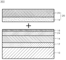
- FIG. 1 is a cross-sectional view illustrating a first display device including a detachable first window structure according to an embodiment of the present invention.
- FIG. 2 is a plan view showing examples of a detachment / attachment pattern applied to a detachable first window structure according to the present invention.
- FIG 3 is a cross-sectional view illustrating a second display device including a detachable first window structure according to the present invention.
- FIG. 4 is a cross-sectional view illustrating a third display device including a second window structure that can be detachably attached according to the present invention.
- FIG. 5 is a cross-sectional view illustrating a fourth display device including a detachable third window structure according to the present invention.
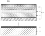
- FIG. 6 is a cross-sectional view illustrating a fifth display device including a fourth window structure capable of being detachably attached according to the present invention.
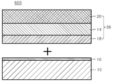
- FIG. 7 is a cross-sectional view illustrating a sixth display device including a fifth window structure capable of being detachably attached according to the present invention.
- Embodiments of the present invention provide a display device that adjusts adhesion and removes bubbles by applying a window structure or touch screen having an adhesive force of 0.1 gf / 25 mm to 500 gf / 25 mm to a display device do.
- the window structure or the touch screen is formed with a detachable pattern to be detachably attached to a touch screen or a display, respectively. Therefore, it can be said that the attached and detached device is associated with the touch screen or the display.
- detachment means that the detachable layer is freely adhered to and detached from the adherend.
- the attachment / detachment pattern of the present invention is limited to being detachably attached to a touch screen and a display, and is clearly distinguished from a conventional window protective film detachably attached to a window. That is, the apparatus of the present invention is not a complete display apparatus of a window or a display apparatus without a touch screen. The display device is completed only when the window or the touch screen of the present invention is attached. By the way, the window protective film is attached on the window of the present invention, and the window protective film is attached to the already completed display. Accordingly, the window or touch screen of the present invention is an essential component of the display device, but the conventional window protective film corresponds to a supplementary component that can be selectively applied to the display device. Accordingly, window protective films are excluded from the scope of the present invention.
- the display device refers to all image processing devices such as a mobile device, an information processing terminal, and a television.
- the mobile device includes a mobile phone, a smart phone, a tablet, and the like.
- the information processing terminal includes an ATM, a kiosk, and the like.
- the display of the display device may be flat or curved, and may be flexible.
- the image processing apparatus includes a window, a touch screen, and a display. Accordingly, the window generally refers to a window of a mobile device, a window of an information processing terminal, or a window of all image processing devices such as a television.
- the touch screen and the display also refer to a touch screen and a display that are applied to all image processing apparatuses.
- the window structure is divided into first to fifth window structures that are detachably attached to the touch screen and the display. That is, the first to fifth window structures are detachably attached to a touch screen, a cover layer of a touch screen, and a display (hereinafter, also referred to as an adherend device).
- the first to fifth window structures will be described separately.
- Embodiments of the present invention provide examples of display devices to which the first to fifth window structures are applied, but may be applied to other types of display devices within the scope of the present invention.
- the window structure of the present invention is separately manufactured and detachably attached to the adherend. At this time, the window structure can be manually attached.
- a window or a touch screen has a detachable pattern, and a corresponding touch screen or display has an adhesion reducing layer.
- the window or touch screen has an adhesion reducing layer, There may be a removable pattern. In this case, the above case was taken as an example.
- FIG. 1 is a cross-sectional view illustrating a first display device 100 including a detachable first window structure according to an embodiment of the present invention.
- a cross-section in the strict sense, and for the convenience of explanation, there may be a component that may not appear on the cross-section.
- the first display device 100 includes a display 10, an adhesive layer 12, a touch screen 14, an adhesion reducing layer 16, a removable pattern 18, and a window 20 sequentially stacked .
- the first window structure 22 including the attachment / detachment pattern 18 and the window 20 is referred to as a first window structure.
- the display 10 includes a liquid crystal display (LCD), an organic light emitting diode (OLED), and an electrophoretic display (EPD), and also utilizes quantum dots.
- the adhesive layer 12 fixes the touch screen 14 to the display 10, for example, a thermosetting adhesive or an ultraviolet curable adhesive can be used. However, the present invention is not limited to this, and an OCA tape or the like can be used.
- the touch screen 14 has a conductive pattern formed on one side or both sides of an insulating layer made of metal oxide or plastic.
- Metal oxide is mainly used for the conductive pattern, and metal oxides include ITO, ATO, ZnO, Cu, conductive polymer, or silver nanowire.
- the window 20 can be used without limitation as long as it is made of a transparent material.
- a glass substrate or a plastic substrate Specifically, the glass substrate may be tempered glass, and the plastic substrate may be made of a material selected from the group consisting of polyethylene terephthalate (PET), polyethylene naphthalate (PEN), polyether sulfone (PES), polyimide (PI), polyarylate polymethyl methacrylate), or COC (cycloolefin copolymer).
- PET polyethylene terephthalate
- PEN polyethylene naphthalate
- PES polyether sulfone
- PI polyimide
- COC cycloolefin copolymer
- the window 20 may have a print layer that is transparent or exhibits various functions.
- the print layer may be formed of any one or more of transparent, translucent, and / or color.
- the printing layer may be formed using inkjet printing or transfer using inkjet printing using silk printing or UV or thermal curing.
- a functional coating layer such as an inner fingerprint coating or an antimicrobial coating or a scratch-resistant coating may be formed.
- the functional coating layer may be formed by dry coating such as wet coating and vapor deposition to apply the coating liquid.
- the glass substrate of the window 20 or the bottom of the plastic substrate may be provided with characteristics such as shielding, reflection prevention, blue light shielding, electromagnetic wave shielding, and privacy.
- the window 20 may have an opening for exposing a button, a camera, a speaker, or the like.
- an adhesion reduction layer 16 may be added on the touch screen 14.
- the adhesion reducing layer 16 lowers the frictional force and increases the slip property.
- the adhesion reducing layer 16 allows the first window structure 22 to be easily detached and attached from the touch screen 14.
- a coating material of a fluorine resin or a silicone resin can be used as the adhesion reducing layer 16.
- the adhesion reducing layer 16 may be formed by depositing TiO 2 or silica (SiO 2 ) on the touch screen 14 and then coating a fluororesin or a silicone resin on the deposited touch screen 14 .
- the fluororesin or silicone resin can be formed by an ECC (Easy Cleaning Coating) method.
- ECC Easy Cleaning Coating
- the adhesion reducing layer 16 When the adhesion reducing layer 16 is applied, generation of bubbles can be more effectively suppressed when the window 20 is attached.
- the adhesion reducing layer 16 allows the consumer to easily attach and detach the first window structure 22 without a separate tool.
- the attachment / detachment pattern 18 has a self-adhesive force.
- the self-adhesive force is a property of attaching / detaching the attachment / detachment pattern 18 to itself without bubbling even if the attachment / detachment pattern 18 is placed on the touch screen 14 alone.
- the adhesion reducing layer 16 when the adhesion reducing layer 16 is applied to the touch screen 14, it has a higher self-adhesive force than when the adhesion reducing layer 16 is absent.
- the adhesive force according to the embodiment of the present invention may vary depending on the presence of the adhesion reducing layer 16.
- the adhesive strength when the adhesion reducing layer 16 is present is 0.5 gf / 25 mm to 500 gf / 25 mm, but the adhesion strength when the adhesion reducing layer 16 is absent is 0.1 gf / 25 mm to 200 gf / 25 mm. It is easier to attach the first window structure 22 without bubbles when the adhesion reducing layer 16 is present when there is the attaching / detaching pattern 18 of the same material and thickness. Also, due to the adhesion reducing layer 16, separation of the first window structure 22 is relatively easy.
- the adhesion reducing layer 16 of the present invention may be in the form of a microprojection formed on all or part of the adhesion reducing layer 16.
- the cross section of the microprojections may be angular, curvilinear, or a combination thereof.
- the adhesion reducing layer 16 on which the fine protrusions are formed has the effect of preventing fingerprints, preventing contamination, preventing reflection, etc., and has an effect of stably attaching / detaching the detachable / attachable pattern 18 by fine protrusions without hindering the clarity of the screen Bring it.
- the adhesion reducing layer 16 of the present invention may include patterns formed of microprojections. It is possible to confirm authenticity and engraved patterns for at least any one of a window, a touch screen, and a display acquired through different paths.
- the detachment pattern 18 is attached to the adhesion reducing layer 16, the fine protrusions and patterns disappear and the adhesion reducing layer 16 becomes transparent.
- FIG. 2 is a plan view showing examples of a removable pattern 18 applied to a detachable first window structure 22 according to an embodiment of the present invention.
- e is an adhesive layer having an adhesive force of about 0.1 gf / 25 mm to 500 gf / 25 mm
- f is a cured layer of e-cured adhesive force lower than the adhesive force of e. That is, e is an adhesive layer capable of curing and f is a curing layer.
- the area occupied by the cured layer (f) may be 5 to 95%.
- the curable pressure-sensitive adhesive layer (e) may be a thermosetting pressure-sensitive adhesive layer or an ultraviolet-curable pressure-sensitive adhesive layer.
- the thermosetting adhesive layer can be variously selected within the scope of the present invention. For example, a resin composition containing a hydroxyl group-containing acrylic resin, an acrylic resin having a hydroxyl group and having a weight average molecular weight of 100,000 to 1,000,000, a resin composition containing a block isocyanate as a main component, a composition containing an acrylic resin containing a hydroxyl group and a block isocyanate as essential components, And a composition containing a block isocyanate and a compound having two or more functional groups in one molecule.
- the ultraviolet ray-curable pressure-sensitive adhesive layer is formed, for example, by blending various acrylic units and an ultraviolet ray curing catalyst into a polyurethane resin, an epoxy resin or a polyester resin.
- an ultraviolet curing material urethane or acrylate oligomer, reactive monomer, photoinitiator and leveling agent are mixed as an ultraviolet reactive coating material.
- the urethane acrylate oligomer has a formula containing an aliphatic, cyclic aliphatic, aromatic compound or an oligomer of these compounds, and polyester polyol or polyether polyol is included in the molecular structure.
- the reactive monomer trimethylpropane triacrylate, hexane diol diacrylate, pentaerythritol triacrylate and dipentaerythritol hexaacrylate are mixed and adjusted at a suitable ratio in consideration of hardness and adhesive force.
- the photoinitiator a usual polymerization initiator which is activated by ultraviolet rays is used, and in particular, hydroxycyclohexyl phenyl ketone, benzophenol, and phenyl-2-hydroxy-2-phenylketone are mainly used.
- the first attachment / detachment patterns 18a, a are arranged in stripe form in the adhesive layer e and the cured layer f which can be cured.
- the order in which the adhesive layer (e) and the cured layer (f) are arranged may vary depending on the shape of the first window structure 22 to which the first attachment / detachment pattern 18a of the present invention is applied.
- the bevel region may be predominantly a cured layer (f).
- the widths of the adhesive layer (e) and the cured layer (f) constituting the first attachment / detachment pattern (18a) can be appropriately adjusted.
- the shape of the band can be changed to a rectangular shape having a constant thickness, or a shape such as a wavy shape in some cases.
- the second attachment / detachment patterns 18b, b are lattice-shaped, and the adhesive layer e and the cured layer f are disposed in the respective gratings.
- the order in which the adhesive layer (e) and the cured layer (f) are arranged may vary depending on the shape of the first window structure 22 to which the second attachment / detachment pattern 18b of the present invention is applied.
- the bevel region may be predominantly a cured layer (f).
- the areas of the adhesive layer (e) and the cured layer (f) constituting the second attachment / detachment pattern (18a) can be appropriately adjusted.
- the shape of the band may be a square shape having a constant thickness, or a shape such as a circle, an ellipse, a wavy shape, or the like depending on the case.
- the third attachment and detachment patterns 18c and 18c are disposed in the form of a fence with the adhesive layer e and the cured layer f being closed.
- the order in which the adhesive layer (e) and the cured layer (f) are arranged may vary depending on the shape of the first window structure 22 to which the third attachment / detachment pattern 18c of the present invention is applied.
- the bevel region may be predominantly a cured layer (f).
- the area of each of the adhesive layer (e) and the cured layer (f) forming the third attachment / detachment pattern (18c) can be appropriately adjusted.
- the shape of the fence may be changed to a rectangular shape having a constant thickness, or a shape such as a wavy shape in some cases.
- the fourth attachment / detachment pattern 18d, d is penetrated through one of the adhesive layer e and the cured layer f on a part of the closed fence of the third attachment / detachment pattern 18c.
- the order in which the adhesive layer (e) and the cured layer (f) are arranged may vary depending on the shape of the first window structure 22 to which the fourth attachment / detachment pattern 18d of the present invention is applied.
- the bevel region may be predominantly a cured layer (f).
- the area of each of the adhesive layer (e) and the cured layer (f) forming the fourth attachment / detachment pattern (18d) can be appropriately adjusted.
- the shape of the fence may be changed to a rectangular shape having a constant thickness, or a shape such as a wavy shape in some cases.
- the attachment / detachment pattern 18 freely adjusts the detachment / adhesion force.
- the adhesive force of the attachment / detachment pattern (18) is changed. Further, since the adhesive layer (e) and the cured layer (f) of the attaching / detaching pattern (18) have mutually different adhesive forces, the space in which bubbles are removed becomes larger.
- the first window structure 22 of the present invention is separately fabricated and protected by a release film.
- the release film is removed.
- the attachment / detachment pattern 18 is exposed.
- the first window structure 22 with the removable pattern 18 exposed is manually attached to the touch screen 14 or the adhesion reducing layer 16 to complete the display on which the window 20 is mounted. Further, in order to break or replace the window 20, the first window structure 22 may be manually separated and a new first window structure 22 may be attached.
- FIG. 3 is a cross-sectional view illustrating a second display device 200 including a detachable first window structure 22 according to an embodiment of the present invention.
- the second display device 200 is the same as the first display device 100 except that the adhesive layer 12 is not provided. In the following description, duplicate descriptions will be omitted or briefly explained.
- the second display device 200 is a sequential layer of the display 10, the touch screen 14, the adhesion reduction layer 16, and the first window structure 22.
- the first window structure 22 includes a removable pattern 18.
- the attachment / detachment pattern 18 is divided into a curable adhesive layer e and a cured adhesive layer c.
- the adhesive layer e and the cured layer f are entirely divided by the cured layer f
- the area may be from 5 to 95%. By varying the area, it is possible to control the adhesive force of the attaching / detaching patterns 18 and facilitate the removal of bubbles.
- the touch screen 14 is formed with a conductive pattern directly on the display 10. That is, the touch screen 14 is formed with a conductive pattern formed on the display 10.
- the first window structure 22 includes the attachment / detachment pattern 18 described above.
- the second display device 200 may include an adhesion reducing layer 16.
- the materials, functions and the like of the adhesion reducing layer 16 are as described in the first display device 100.
- the adhesive force according to the embodiment of the present invention may vary depending on the presence of the adhesion reducing layer 16.
- the adhesive strength when the adhesion reducing layer 16 is present is 0.5 gf / 25 mm to 500 gf / 25 mm, but the adhesion strength when the adhesion reducing layer 16 is absent is 0.1 gf / 25 mm to 200 gf / 25 mm.
- the window structure 20 of the first window structure 22 may further include additional elements for imparting various functions between the attachment and detachment patterns 18.
- the additional element may include a transparent adhesive layer (OCA), a scattering-preventive layer, etc., and if necessary, a printing layer and a functional coating layer may be appropriately formed.
- OCA transparent adhesive layer
- a scattering-preventive layer etc.
- a printing layer and a functional coating layer may be appropriately formed.
- the removable pattern 18 may be formed on the transparent synthetic resin film.
- FIG. 4 is a cross-sectional view illustrating a third display device 300 including a detachable second window structure 26 according to an embodiment of the present invention.
- the third display device 300 is the same as the first display device 100 except that the touch screen cover layer 24 is introduced. Accordingly, detailed description of the same reference numerals will be omitted.
- the second window structure 26 may further include an additional element as shown in the first window structure 22.
- the third display device 300 includes a display 10, an adhesive layer 12, a touch screen 14, a cover layer 24, an adhesion reducing layer 16, a removable pattern 18, (20) may be sequentially stacked.
- the third display device 300 may be directly bonded to the display 10 and the touch screen 14 without the adhesive layer 12, such as the second display device 200.
- the second window structure 26 includes a detachment / attaching pattern 18.
- the attachment / detachment pattern 18 is divided into a curable adhesive layer e and a cured adhesive layer c.
- the adhesive layer e and the cured layer f are entirely divided by the cured layer f
- the area may be from 5 to 95%. By varying the area, it is possible to control the adhesive force of the attachment / detachment pattern 18 and facilitate the removal of bubbles
- a conductive pattern for forming the touch screen 14 is disposed on the upper portion or the lower portion of the cover layer 24.
- the cover layer 24 can be seen as part of the touch screen 14.
- the cover layer 24 prevents the touch screen 14 from being damaged by impact or contamination.
- the third display device 300 may have a conductive pattern formed directly on the display 10 to form a touch screen 14 at which the touch screen cover layer 24 may be located at the top of the display 10 .
- the cover layer 24 When the cover layer 24 is covered with the second window structure 26, it is located inside the third display device 300. Since the cover layer 22 is located inside, the cover layer 24 is exposed to the outside of the third display device 300, and there is no possibility that the cover layer 24 is damaged by a shock or the like.
- the cover layer 24 may be a print layer or a functional coating layer, and may enable the third display device 300 to be beautiful through various designs or translucency.
- the cover layer 24 can eliminate the influence of the curvature and the step difference due to various patterns, circuits, etc. of the touch screen 14. When the influence of the bending or the step difference disappears, detachment and attachment by the attaching / detaching pattern 18 becomes easier.
- the cover layer 24 can be made of any transparent material without limitation.
- a glass substrate or a plastic substrate may be tempered glass or unreinforced glass
- the plastic substrate may be made of PET (polyethylene terephthalate), polyethylene naphthalate (PEN), polyether sulfone (PES), polyimide (PI), polyarylate polycarbonate, PMMA (polymethyl methacrylate), or COC (cycloolefin copolymer).
- PET polyethylene terephthalate
- PEN polyethylene naphthalate
- PES polyether sulfone
- PI polyimide
- PMMA polymethyl methacrylate
- COC cycloolefin copolymer
- the third display device 300 may include an adhesion reducing layer 16.
- the materials, functions and the like of the adhesion reducing layer 16 are as described in the first display device 100.
- the adhesive force according to the embodiment of the present invention may vary depending on the presence of the adhesion reducing layer 16.
- the adhesive strength when the adhesion reducing layer 16 is present is 0.5 gf / 25 mm to 500 gf / 25 mm, but the adhesion strength when the adhesion reducing layer 16 is absent is 0.1 gf / 25 mm to 200 gf / 25 mm.
- the adhesion reducing layer 16 When there is the attachment / detachment pattern 18 of the same material and thickness, if the adhesion reducing layer 16 is present, it is easy to attach the second window structure 26 without bubbles. Also, due to the adhesion reducing layer 16, the separation of the second window structure 26 is relatively easy.
- the attachment / detachment pattern 18 has a self-adhesive force.
- the self-adhesive force is a property of attaching / detaching the attachment / detachment pattern 18 to itself without bubbling even if the attachment / detachment pattern 18 is placed on the touch screen cover layer 24 alone.
- applying the adhesion reducing layer 16 to the touch screen cover layer 24 has a better magnetic adhesion than when the adhesion reducing layer 16 is absent.
- the display devices according to the embodiment of the present invention are replaced when the window structure is broken and selected and attached to the new window structure. Specifically, it is replaced when the broken window structure is detached and a new window structure is attached. Replacement of the window structure can be performed manually by the customer, and the replacement time is very short. In addition, since only the window structure is removed, the display device can be easily recycled. Furthermore, since the window structure is detachable, it can be easily attached without bubbles. Since the manufacturer needs only to manufacture the part other than the window structure and does not need to perform the bonding step, the manufacturing process is simplified.
- FIG. 5 is a cross-sectional view illustrating a fourth display device 400 including a detachable third window structure 30 according to an embodiment of the present invention.
- the fourth display device 400 is basically the same as the first display device 100 except that the position of each layer is changed. In the following description, duplicate descriptions will be omitted or briefly explained.
- the fourth display device 400 includes a display 10, an adhesion reducing layer 16, a removable pattern 18, a touch screen 14, an adhesive layer 12, and a window 20 sequentially stacked .
- the window 20, the adhesive layer 12, the touch screen 14, and the attachment / detachment pattern 18 constitute the third window structure 30.
- the third window structure 30 includes a removable pattern 18.
- the attachment / detachment pattern 18 is divided into a curable adhesive layer e and a cured adhesive layer c.
- the adhesive layer e and the cured layer f are entirely divided by the cured layer f
- the area may be from 5 to 95%. By varying the area, it is possible to control the adhesive force of the attaching / detaching patterns 18 and facilitate the removal of bubbles.
- the display 10 includes a liquid crystal display (LCD), an organic light emitting diode (OLED), and an electrophoretic display (EPD), and also utilizes quantum dots.
- the adhesive layer 12 for example, a thermosetting adhesive or an ultraviolet curable adhesive may be used. However, the present invention is not limited to this, and an OCA tape or the like can be used.
- the touch screen 14 has a conductive pattern formed on one side or both sides of an insulating layer made of metal oxide or plastic. Metal oxide is mainly used for the conductive pattern, and metal oxides include ITO, ATO, ZnO, Cu, conductive polymer, or silver nanowire.
- an adhesion reducing layer 16 may be added on the display 10.
- the adhesion reducing layer 16 increases the slip property by increasing the contact angle.
- the adhesion reducing layer 16 allows the third window structure 30 to be easily detached and attached from the touch screen 14.
- a coating material of a fluorine resin or a silicone resin can be used as the adhesion reducing layer 16.
- the adhesion reducing layer 16 may be formed by depositing TiO 2 or silica (SiO 2 ) on the display 10 and then coating a fluororesin or a silicone resin on the deposited display 10. At this time, the fluororesin or silicone resin can be formed by an ECC (Easy Cleaning Coating) method.
- ECC Easy Cleaning Coating
- the attachment / detachment pattern 18 has a self-adhesive force.
- the self-adhesive force is a property of attaching / detaching the attachment / detachment pattern 18 to itself without bubbling even if the attachment / detachment pattern 18 is placed on the touch screen 14 alone.
- the adhesion reducing layer 16 is applied to the display 10, it has a higher magnetic adhesion than when the adhesion reducing layer 16 is absent.
- the adhesive force according to the embodiment of the present invention may vary depending on the presence of the adhesion reducing layer 16.
- the adhesive force is 0.5 gf / 25 mm to 500 gf / 25 mm. If there is no adhesion reducing layer 16, the adhesion is 0.1 gf / 25 mm to 200 gf / 25 mm.
- the attachment / detachment pattern 18 of the same material and thickness if the adhesion reducing layer 16 is present, it is easy to attach the third window structure 30 without bubbles. Also, due to the adhesion reducing layer 16, the separation of the third window structure 30 is relatively easy.
- the third window structure 30 of the present invention is separately manufactured and protected by a release film.
- the release film is removed.
- the attachment / detachment pattern 18 is exposed.
- the third window structure 30, in which the attachment / detachment pattern 18 is exposed is manually attached to the display 10, the display on which the window 20 is mounted can be completed. Accordingly, unlike the prior art, a precise bonding process is not required. Also, in order to break or replace the third window structure 30, the third window structure 30 may be manually separated and a new third window structure 30 may be attached.
- FIG. 6 is a cross-sectional view illustrating a fifth display device 500 including a detachable fourth window structure 34 according to an embodiment of the present invention.
- the fifth display device 500 is the same as the first display device 100 except that the adhesive layer 12 is replaced with a removable layer 32. In the following description, duplicate descriptions will be omitted or briefly explained.
- the fourth window structure (34) includes a detachment / attaching pattern (18).
- the attachment / detachment pattern 18 is divided into a curable adhesive layer e and a cured adhesive layer c.
- the adhesive layer e and the cured layer f are entirely divided by the cured layer f
- the area may be from 5 to 95%.
- the attachable / detachable layer 32 has the same function and function, but has a different position because of its different reference numeral.
- the fourth window structure 34 is detachably attached to the display 10 by the attachment / detachment pattern 18.
- the attachment / detachment pattern 18 can be attached to the display 10 with the release film removed.
- the fourth window structure 34 can be attached to and detached from the touch screen 14 by a removable layer 32.
- the fourth window structure 34 has a removable pattern 18 and a removable layer 32 that can be detachably attached to the display 10 and the touch screen 20, respectively.
- the removable layer 32 may be any transparent material, but may be an acryl-based polymer, a silicone-based polymer, a urethane-based polymer, a pressure-sensitive adhesive mixed with a crosslinking agent in a UV-curable resin, or a mixture thereof or a copolymer thereof.
- the attachment / detachment layer 32 may each be a single layer, or may be a multi-layered or a single layer of different materials for each layer. Depending on the environment in which each of the release layer 32 of the present invention is used, the multi-layer can appropriately select the material constituting each layer.
- the thickness of each of the attachable / detachable layers 32 may be as long as the adhesion is sufficient, preferably 10 to 200 mu m. It will be appreciated that the thickness can be obtained through repeated experiments by those of ordinary skill in the art.
- the window 20 of the third and fourth window structures 30 and 34 and the removable layer 32 or between the touch screen 14 and the removable pattern 18 of the embodiment of the present invention may further include additional elements that impart various functions to any one or both of them.
- the additional element may include a transparent adhesive layer (OCA), a scattering-preventive layer, etc., and if necessary, a printing layer and a functional coating layer may be appropriately formed.
- OCA transparent adhesive layer
- a scattering-preventive layer etc.
- a printing layer and a functional coating layer may be appropriately formed.
- the removable pattern 18 may be formed on the transparent synthetic resin film.
- FIG. 7 is a cross-sectional view illustrating a sixth display device 600 including a fifth window structure 36 detachably attachable according to an embodiment of the present invention.
- the sixth display device 600 is the same as the fourth display device 400 except that the adhesive layer 12 is not provided. Accordingly, detailed description of the same reference numerals will be omitted.
- the fifth window structure 36 may further include an additional element, as shown in the third window structure 30.
- the sixth display device 600 is formed by stacking a display 10, an adhesion reducing layer 16, a removable pattern 18, a touch screen 14, and a window 20.
- the window 20, the touch screen 14, and the removable layer 18 form the fifth window structure 36.
- the fifth window structure 36 includes a detachment / attaching pattern 18.
- the attachment / detachment pattern 18 is divided into a curable adhesive layer e and a cured adhesive layer c.
- the adhesive layer e and the cured layer f are entirely divided by the cured layer f
- the area may be from 5 to 95%. By varying the area, it is possible to control the adhesive force of the attaching / detaching patterns 18 and facilitate the removal of bubbles.
- the touch screen 14 is formed with a conductive pattern directly under the window 20. That is, the touch screen 14 is formed together with the conductive pattern formed on the window 20.
- the sixth display device 600 may include an adhesion reducing layer 16.
- the material, function, etc. of the adhesion reducing layer 16 are as described in the fourth display device 400.
- the adhesive force according to the embodiment of the present invention may vary depending on the presence of the adhesion reducing layer 16.
- the adhesive strength when the adhesion reducing layer 16 is present is 0.5 gf / 25 mm to 500 gf / 25 mm, but the adhesion strength when the adhesion reducing layer 16 is absent is 0.1 gf / 25 mm to 200 gf / 25 mm.
- the attachment / detachment pattern 18 has a self-adhesive force.
- the self-adhesive force is a property of attaching / detaching the attachment / detachment pattern 18 to itself without bubbling even if the attachment / detachment pattern 18 is placed on the display 10 alone.
- application of the adhesion reducing layer 16 to the display 10 has a better magnetic adhesion than when the adhesion reducing layer 16 is absent.
- connection of the first to fifth window structures 22, 26, 30, 34, 36 When applying the first to fifth window structures 22, 26, 30, 34, 36, an electrical connection can be made to face each other in a predetermined area of each of the display 10 and the touch screen 14. For the connection, a part of the attachment / detachment pattern 18 of the touch screen 14 can be removed.
- the connection portions When the first to fifth window structures 22, 26, 30, 34, 36 are attached to the touch screen 14 and the display 10, the connection portions are connected to each other. In this case, connection of the first to sixth display devices 100, 200, 300, 400, 500, 600 can be realized.
- the display devices according to the embodiment of the present invention are replaced when the window structure is broken and selected and attached to the new window structure. Specifically, it is replaced when the broken window structure is detached and a new window structure is attached.
- the replacement process of the window structure can be carried out directly by the customer, and the replacement time is very short.
- the display device can be easily recycled.
- the window structure is detachably attached by adhesion, it can be easily attached without bubbles. Since the manufacturer needs only to manufacture the part other than the window structure and does not need to perform the bonding step, the manufacturing process is simplified. Particularly, in the presence of the adhesion reduction layer, the window structure is easier to adhere without bubbles, and the window structure is relatively easily separated by the influence of the adhesion reduction layer.
- the display device of the present invention can be designed variously in appearance.
- the display device of the present invention can be designed in a beautiful shape, various colors and patterns. This is because, by separating the original window structure and attaching a new structure, you can change the appearance of the window structure to the desired design. Conventionally, in order to change the design, the adhesion of the window structure must be dismantled and the new window structure must be adhered again.
- the display device of the present invention changes design when a conventional window structure is detached and a new window structure is attached. Accordingly, the window structure of the present invention is not a necessity fixed to the display device, unlike the prior art, and can be treated as a consumable item which can be detached and attached as needed. In this way, if the design is diversified, the manufacturer of the display device does not have to provide service afterwards in response to the design.
- detachment of the window with the detachment pattern having the adhesive force of 0.1 gf / 25 mm to 500 gf / 25 mm is easily carried out, . It is possible to control the adhesive strength of the removable pattern 18 and facilitate removal of the bubbles by changing the area of the adhesive layer e and the cured layer f of the removable pattern. So that it can be easily attached and detached without bubbles.
- the display device of the present invention is simple in manufacturing process, low in manufacturing cost, and can be designed in various ways to meet the needs of consumers. Furthermore, since the window is easily replaced with a removable one, it can be handled as a one-time consumable, not a necessity fixed to the display device.
- the first to sixth display devices are 100, 200, 300, 400, 500, 600;
- the first to sixth display devices are 100, 200, 300, 400, 500, 600;
- the first to sixth display devices are 100, 200, 300, 400, 500, 600;
Landscapes
- Engineering & Computer Science (AREA)
- General Engineering & Computer Science (AREA)
- Theoretical Computer Science (AREA)
- Human Computer Interaction (AREA)
- Physics & Mathematics (AREA)
- General Physics & Mathematics (AREA)
- Devices For Indicating Variable Information By Combining Individual Elements (AREA)
- Liquid Crystal (AREA)
- Position Input By Displaying (AREA)
Abstract
Description
Claims (12)
- 윈도우 및 디스플레이를 포함하고, 터치스크린이 선택적으로 포함되어 이루어지고, 탈부착 패턴을 가진 디스플레이 장치에 있어서,상기 윈도우, 터치스크린 및 디스플레이의 어느 하나에 위치하고, 접착력이 0.1gf/25mm 내지 500gf/25mm인 탈부착 패턴을 포함하고,상기 탈부착 패턴은 점착층 및 경화층을 포함하고, 상기 점착층이 상기 탈부착 패턴에서 차지하는 면적이 5~95%인 것을 특징으로 하는 탈부착 패턴을 가진 디스플레이 장치.
- 제1항에 있어서, 상기 탈부착 패턴은 상기 점착층은 열 또는 자외선에 의해 경화가 가능한 것을 특징으로 하는 탈부착 패턴을 가진 디스플레이 장치.
- 제1항에 있어서, 상기 탈부착 패턴은 상기 점착층 및 상기 경화층이 띠 형태로 배치되는 것을 특징으로 하는 탈부착 패턴을 가진 디스플레이 장치.
- 제1항에 있어서, 상기 탈부착 패턴은 상기 점착층 및 상기 경화층이 격자 형태로 배치되는 것을 특징으로 하는 탈부착 패턴을 가진 디스플레이 장치.
- 제1항에 있어서, 상기 탈부착 패턴은 상기 점착층 및 상기 경화층이 울타리 형태로 폐쇄되도록 배치되는 것을 특징으로 하는 탈부착 패턴을 가진 디스플레이 장치.
- 제1항에 있어서, 상기 탈부착 패턴은 상기 점착층 및 상기 경화층이 울타리 형태를 이루고 상기 울타리의 일부는 폐쇄되고 일부는 개방되도록 배치되는 것을 특징으로 하는 탈부착 패턴을 가진 디스플레이 장치.
- 제3항 내지 제5항의 어느 한 항에 있어서, 상기 띠 형태, 상기 격자 형태 또는 상기 울타리 형태 중의 적어도 어느 하나는 사각 형태 또는 물결 형태 또는 그들의 조합인 것을 특징으로 하는 탈부착 패턴을 가진 디스플레이 장치.
- 제1항에 있어서, 상기 탈부착 패턴은 접착감소층에 탈부착되고, 상기 접착감소층은 상기 탈부착 패턴이 상기 접착감소층에 탈부착되는 접착력을 감소시키는 것을 특징으로 하는 탈부착 패턴을 가진 디스플레이 장치.
- 제8항에 있어서, 상기 접착감소층은 불소계 수지 또는 실리콘계 수지를 포함하는 것을 특징으로 하는 탈부착 패턴을 가진 디스플레이 장치.
- 제8항에 있어서, 상기 접착감소층은 티타니아(TiO2) 혹은 실리카(SiO2)로 이루어진 증착층 및 상기 증착층 상에 불소계 수지 또는 실리콘계 수지가 포함된 층이 위치하는 것을 특징으로 하는 탈부착 패턴을 가진 디스플레이 장치.
- 제8항에 있어서, 상기 접착감소층의 전부 또는 일부에는 미세돌기를 포함하는 것을 특징으로 하는 탈부착 패턴을 가진 디스플레이 장치.
- 제8항에 있어서, 상기 탈부착층 또는 상기 접착감소층의 어느 하나는 상기 터치스크린 상에 위치하는 터치스크린 커버층 상에 존재하는 것을 특징으로 하는 탈부착 패턴을 가진 디스플레이 장치.
Priority Applications (4)
| Application Number | Priority Date | Filing Date | Title |
|---|---|---|---|
| US16/649,358 US11073924B2 (en) | 2016-10-03 | 2018-08-27 | Apparatus of display having detachable pattern |
| EP18859062.4A EP3686716B1 (en) | 2016-10-03 | 2018-08-27 | Display device having attachable/detachable pattern |
| CN201880060637.6A CN111095177A (zh) | 2016-10-03 | 2018-08-27 | 具有可拆卸图案的显示装置 |
| JP2020516383A JP2020534577A (ja) | 2016-10-03 | 2018-08-27 | 着脱パターンを有するディスプレイ装置 |
Applications Claiming Priority (3)
| Application Number | Priority Date | Filing Date | Title |
|---|---|---|---|
| KR20160127307 | 2016-10-03 | ||
| KR1020170123028A KR102146150B1 (ko) | 2016-10-03 | 2017-09-23 | 탈부착 패턴을 가진 디스플레이 장치 |
| KR10-2017-0123028 | 2017-09-23 |
Publications (1)
| Publication Number | Publication Date |
|---|---|
| WO2019059546A1 true WO2019059546A1 (ko) | 2019-03-28 |
Family
ID=61975938
Family Applications (1)
| Application Number | Title | Priority Date | Filing Date |
|---|---|---|---|
| PCT/KR2018/009859 Ceased WO2019059546A1 (ko) | 2016-10-03 | 2018-08-27 | 탈부착 패턴을 가진 디스플레이 장치 |
Country Status (6)
| Country | Link |
|---|---|
| US (1) | US11073924B2 (ko) |
| EP (1) | EP3686716B1 (ko) |
| JP (1) | JP2020534577A (ko) |
| KR (1) | KR102146150B1 (ko) |
| CN (1) | CN111095177A (ko) |
| WO (1) | WO2019059546A1 (ko) |
Families Citing this family (8)
| Publication number | Priority date | Publication date | Assignee | Title |
|---|---|---|---|---|
| KR102241293B1 (ko) * | 2018-05-14 | 2021-04-16 | 김영수 | 점착조절층을 이용한 표시장치 |
| WO2019221460A1 (ko) * | 2018-05-14 | 2019-11-21 | Kim Young Su | 점착조절층을 이용한 표시장치 |
| WO2020040489A1 (ko) * | 2018-08-20 | 2020-02-27 | 김영수 | 배면커버를 포함하는 탈부착 표시장치 |
| KR102241276B1 (ko) * | 2018-08-20 | 2021-04-16 | 김영수 | 일체형 커버를 포함하는 탈부착 표시장치 |
| KR102437333B1 (ko) * | 2019-12-20 | 2022-08-29 | 김영수 | 복합커버층을 포함하는 탈부착 표시장치 |
| WO2021125764A1 (ko) * | 2019-12-20 | 2021-06-24 | 김영수 | 복합커버층을 포함하는 탈부착 표시장치 |
| KR102776785B1 (ko) | 2020-04-22 | 2025-03-11 | 삼성디스플레이 주식회사 | 표시 장치 및 표시 장치의 제조 방법 |
| KR102395757B1 (ko) * | 2021-01-28 | 2022-05-10 | (주)유티아이 | 플렉시블 커버 윈도우 |
Citations (6)
| Publication number | Priority date | Publication date | Assignee | Title |
|---|---|---|---|---|
| US20100066683A1 (en) * | 2008-09-17 | 2010-03-18 | Shih-Chang Chang | Method for Transferring Thin Film to Substrate |
| KR20120055454A (ko) * | 2010-11-22 | 2012-05-31 | (주)엘지하우시스 | 양면 점착 시트 및 이를 포함하는 터치 패널 표시장치 |
| KR20130003829A (ko) * | 2011-07-01 | 2013-01-09 | 김영수 | 터치스크린 패널 보호용 필터 |
| KR20150034829A (ko) * | 2013-08-30 | 2015-04-06 | 주식회사 엔씰텍 | 플렉시블 정보 표시 소자 제조용 지지 기판, 이의 제조 방법, 이를 이용하여 제조된 플렉시블 정보 표시 소자 및 이의 제조방법 |
| KR101574923B1 (ko) | 2015-01-20 | 2015-12-04 | 김영수 | 탈부착이 가능한 윈도우를 포함하는 디스플레이 장치 및 그 탈부착 방법 |
| KR20160120436A (ko) * | 2015-04-08 | 2016-10-18 | 김영수 | 탈부착층을 가진 디스플레이 장치 및 그 제조방법 |
Family Cites Families (11)
| Publication number | Priority date | Publication date | Assignee | Title |
|---|---|---|---|---|
| DE60136873D1 (de) * | 2000-04-24 | 2009-01-15 | Avery Dennison Corp | Klebstoffartikel mit verbessertem Luftaustritt und Verfahren zu deren Herstellung |
| JP2008027747A (ja) * | 2006-07-21 | 2008-02-07 | Fujitsu Ltd | 電池充電用燃料電池 |
| JP5269343B2 (ja) * | 2007-04-27 | 2013-08-21 | 株式会社半導体エネルギー研究所 | 半導体装置の作製方法 |
| JP2013125262A (ja) * | 2011-12-16 | 2013-06-24 | Technology Research Association For Advanced Display Materials | 貼合材料、表示素子及び表示素子の製造方法 |
| KR20140123735A (ko) * | 2013-04-15 | 2014-10-23 | 삼성디스플레이 주식회사 | 점착캡슐을 갖는 점착제 및 상기 점착제에 의하여 형성된 점착층을 갖는 유기발광 표시장치 |
| CN105446508B (zh) * | 2014-06-19 | 2018-12-25 | 宸鸿科技(厦门)有限公司 | 触控显示装置 |
| KR102246292B1 (ko) * | 2014-07-29 | 2021-04-30 | 삼성디스플레이 주식회사 | 휴대용 전자장치 |
| KR101562874B1 (ko) * | 2014-12-03 | 2015-10-26 | 엘지디스플레이 주식회사 | 보호 필름 및 그를 포함한 디스플레이 모듈과 그 제조 방법 |
| JP6460525B2 (ja) * | 2015-01-30 | 2019-01-30 | 藤森工業株式会社 | 接着性樹脂層、接着性樹脂フィルム、積層体及び積層体の製造方法 |
| KR102342869B1 (ko) * | 2015-02-26 | 2021-12-23 | 삼성디스플레이 주식회사 | 가요성 표시 장치 및 이의 제조방법 |
| KR101959632B1 (ko) * | 2016-10-03 | 2019-03-18 | 김영수 | 탈부착 조절을 위한 미세돌기를 포함하는 디스플레이 장치 및 그 제조방법 |
-
2017
- 2017-09-23 KR KR1020170123028A patent/KR102146150B1/ko not_active Expired - Fee Related
-
2018
- 2018-08-27 EP EP18859062.4A patent/EP3686716B1/en active Active
- 2018-08-27 JP JP2020516383A patent/JP2020534577A/ja active Pending
- 2018-08-27 WO PCT/KR2018/009859 patent/WO2019059546A1/ko not_active Ceased
- 2018-08-27 CN CN201880060637.6A patent/CN111095177A/zh active Pending
- 2018-08-27 US US16/649,358 patent/US11073924B2/en not_active Expired - Fee Related
Patent Citations (6)
| Publication number | Priority date | Publication date | Assignee | Title |
|---|---|---|---|---|
| US20100066683A1 (en) * | 2008-09-17 | 2010-03-18 | Shih-Chang Chang | Method for Transferring Thin Film to Substrate |
| KR20120055454A (ko) * | 2010-11-22 | 2012-05-31 | (주)엘지하우시스 | 양면 점착 시트 및 이를 포함하는 터치 패널 표시장치 |
| KR20130003829A (ko) * | 2011-07-01 | 2013-01-09 | 김영수 | 터치스크린 패널 보호용 필터 |
| KR20150034829A (ko) * | 2013-08-30 | 2015-04-06 | 주식회사 엔씰텍 | 플렉시블 정보 표시 소자 제조용 지지 기판, 이의 제조 방법, 이를 이용하여 제조된 플렉시블 정보 표시 소자 및 이의 제조방법 |
| KR101574923B1 (ko) | 2015-01-20 | 2015-12-04 | 김영수 | 탈부착이 가능한 윈도우를 포함하는 디스플레이 장치 및 그 탈부착 방법 |
| KR20160120436A (ko) * | 2015-04-08 | 2016-10-18 | 김영수 | 탈부착층을 가진 디스플레이 장치 및 그 제조방법 |
Non-Patent Citations (1)
| Title |
|---|
| See also references of EP3686716A4 |
Also Published As
| Publication number | Publication date |
|---|---|
| JP2020534577A (ja) | 2020-11-26 |
| KR20180037108A (ko) | 2018-04-11 |
| US11073924B2 (en) | 2021-07-27 |
| EP3686716A1 (en) | 2020-07-29 |
| US20200225781A1 (en) | 2020-07-16 |
| KR102146150B1 (ko) | 2020-08-19 |
| CN111095177A (zh) | 2020-05-01 |
| EP3686716B1 (en) | 2023-07-19 |
| EP3686716A4 (en) | 2020-11-04 |
Similar Documents
| Publication | Publication Date | Title |
|---|---|---|
| KR101574923B1 (ko) | 탈부착이 가능한 윈도우를 포함하는 디스플레이 장치 및 그 탈부착 방법 | |
| US11073924B2 (en) | Apparatus of display having detachable pattern | |
| KR101675225B1 (ko) | 탈부착층을 가진 디스플레이 장치 및 그 제조방법 | |
| WO2019059548A1 (ko) | 표면개질 탈부착 시트를 포함하는 디스플레이 장치 | |
| WO2019059551A1 (ko) | 미세돌기 문양을 가진 접착감소층을 포함하는 디스플레이 장치 | |
| KR20180037088A (ko) | 탈부착층을 포함하는 디스플레이 장치 및 그 제조방법 | |
| WO2017150778A1 (ko) | 곡면부를 가진 휴대기기에 부착되는 복합 보호시트 및 그 제조방법 | |
| KR102241293B1 (ko) | 점착조절층을 이용한 표시장치 | |
| KR101911698B1 (ko) | 탈부착 유동층을 가진 디스플레이 장치 | |
| US11324133B2 (en) | Attachable/detachable display device comprising polarizing film | |
| WO2019103439A1 (ko) | 편광필름을 포함하는 탈부착 디스플레이 장치 | |
| KR20180026830A (ko) | 탈부착층을 가진 디스플레이 장치 | |
| KR102144652B1 (ko) | 탈부착 패턴을 가진 디스플레이 장치 | |
| EP3293568A1 (en) | Display device having detachable layer and method for manufacturing the same | |
| KR20180037103A (ko) | 탈부착 시트를 포함하는 디스플레이 장치 | |
| WO2018066833A1 (ko) | 탈부착 유동층을 가진 디스플레이 장치 | |
| JP6330871B2 (ja) | 着脱層を有するディスプレイ装置、及びその製造方法{Apparatus of display having detachable layer and method of manufacturing the display} | |
| WO2018066854A1 (ko) | 탈부착 시트를 포함하는 디스플레이 장치 | |
| WO2019059554A1 (ko) | 은폐문양을 포함하는 디스플레이 장치의 투명부재 및 그 제조방법 | |
| WO2018066853A1 (ko) | 탈부착 조절을 위한 미세돌기를 포함하는 디스플레이 장치 및 그 제조방법 | |
| WO2018117460A1 (ko) | 보호시트를 부착하기 위한 곡면 휴대기기 | |
| WO2021125764A1 (ko) | 복합커버층을 포함하는 탈부착 표시장치 | |
| WO2020111642A1 (ko) | 탈부착 윈도우가 탈부착되는 표시장치의 윈도우 분리형 모듈 | |
| WO2019221460A1 (ko) | 점착조절층을 이용한 표시장치 |
Legal Events
| Date | Code | Title | Description |
|---|---|---|---|
| 121 | Ep: the epo has been informed by wipo that ep was designated in this application |
Ref document number: 18859062 Country of ref document: EP Kind code of ref document: A1 |
|
| ENP | Entry into the national phase |
Ref document number: 2020516383 Country of ref document: JP Kind code of ref document: A |
|
| NENP | Non-entry into the national phase |
Ref country code: DE |
|
| WWE | Wipo information: entry into national phase |
Ref document number: 2018859062 Country of ref document: EP |
|
| ENP | Entry into the national phase |
Ref document number: 2018859062 Country of ref document: EP Effective date: 20200423 |