WO2019073896A1 - 位相変調装置 - Google Patents
位相変調装置 Download PDFInfo
- Publication number
- WO2019073896A1 WO2019073896A1 PCT/JP2018/037206 JP2018037206W WO2019073896A1 WO 2019073896 A1 WO2019073896 A1 WO 2019073896A1 JP 2018037206 W JP2018037206 W JP 2018037206W WO 2019073896 A1 WO2019073896 A1 WO 2019073896A1
- Authority
- WO
- WIPO (PCT)
- Prior art keywords
- pixel
- blank area
- pixel electrode
- drive voltage
- pixel block
- Prior art date
- Legal status (The legal status is an assumption and is not a legal conclusion. Google has not performed a legal analysis and makes no representation as to the accuracy of the status listed.)
- Ceased
Links
Images

Classifications
-
- G—PHYSICS
- G02—OPTICS
- G02F—OPTICAL DEVICES OR ARRANGEMENTS FOR THE CONTROL OF LIGHT BY MODIFICATION OF THE OPTICAL PROPERTIES OF THE MEDIA OF THE ELEMENTS INVOLVED THEREIN; NON-LINEAR OPTICS; FREQUENCY-CHANGING OF LIGHT; OPTICAL LOGIC ELEMENTS; OPTICAL ANALOGUE/DIGITAL CONVERTERS
- G02F1/00—Devices or arrangements for the control of the intensity, colour, phase, polarisation or direction of light arriving from an independent light source, e.g. switching, gating or modulating; Non-linear optics
- G02F1/01—Devices or arrangements for the control of the intensity, colour, phase, polarisation or direction of light arriving from an independent light source, e.g. switching, gating or modulating; Non-linear optics for the control of the intensity, phase, polarisation or colour
- G02F1/13—Devices or arrangements for the control of the intensity, colour, phase, polarisation or direction of light arriving from an independent light source, e.g. switching, gating or modulating; Non-linear optics for the control of the intensity, phase, polarisation or colour based on liquid crystals, e.g. single liquid crystal display cells
- G02F1/133—Constructional arrangements; Operation of liquid crystal cells; Circuit arrangements
- G02F1/136—Liquid crystal cells structurally associated with a semi-conducting layer or substrate, e.g. cells forming part of an integrated circuit
- G02F1/1362—Active matrix addressed cells
- G02F1/136277—Active matrix addressed cells formed on a semiconductor substrate, e.g. of silicon
-
- G—PHYSICS
- G02—OPTICS
- G02F—OPTICAL DEVICES OR ARRANGEMENTS FOR THE CONTROL OF LIGHT BY MODIFICATION OF THE OPTICAL PROPERTIES OF THE MEDIA OF THE ELEMENTS INVOLVED THEREIN; NON-LINEAR OPTICS; FREQUENCY-CHANGING OF LIGHT; OPTICAL LOGIC ELEMENTS; OPTICAL ANALOGUE/DIGITAL CONVERTERS
- G02F1/00—Devices or arrangements for the control of the intensity, colour, phase, polarisation or direction of light arriving from an independent light source, e.g. switching, gating or modulating; Non-linear optics
- G02F1/01—Devices or arrangements for the control of the intensity, colour, phase, polarisation or direction of light arriving from an independent light source, e.g. switching, gating or modulating; Non-linear optics for the control of the intensity, phase, polarisation or colour
- G02F1/13—Devices or arrangements for the control of the intensity, colour, phase, polarisation or direction of light arriving from an independent light source, e.g. switching, gating or modulating; Non-linear optics for the control of the intensity, phase, polarisation or colour based on liquid crystals, e.g. single liquid crystal display cells
- G02F1/133—Constructional arrangements; Operation of liquid crystal cells; Circuit arrangements
- G02F1/1333—Constructional arrangements; Manufacturing methods
- G02F1/1335—Structural association of cells with optical devices, e.g. polarisers or reflectors
- G02F1/133553—Reflecting elements
-
- G—PHYSICS
- G02—OPTICS
- G02B—OPTICAL ELEMENTS, SYSTEMS OR APPARATUS
- G02B5/00—Optical elements other than lenses
- G02B5/30—Polarising elements
-
- G—PHYSICS
- G02—OPTICS
- G02F—OPTICAL DEVICES OR ARRANGEMENTS FOR THE CONTROL OF LIGHT BY MODIFICATION OF THE OPTICAL PROPERTIES OF THE MEDIA OF THE ELEMENTS INVOLVED THEREIN; NON-LINEAR OPTICS; FREQUENCY-CHANGING OF LIGHT; OPTICAL LOGIC ELEMENTS; OPTICAL ANALOGUE/DIGITAL CONVERTERS
- G02F1/00—Devices or arrangements for the control of the intensity, colour, phase, polarisation or direction of light arriving from an independent light source, e.g. switching, gating or modulating; Non-linear optics
- G02F1/01—Devices or arrangements for the control of the intensity, colour, phase, polarisation or direction of light arriving from an independent light source, e.g. switching, gating or modulating; Non-linear optics for the control of the intensity, phase, polarisation or colour
- G02F1/13—Devices or arrangements for the control of the intensity, colour, phase, polarisation or direction of light arriving from an independent light source, e.g. switching, gating or modulating; Non-linear optics for the control of the intensity, phase, polarisation or colour based on liquid crystals, e.g. single liquid crystal display cells
- G02F1/133—Constructional arrangements; Operation of liquid crystal cells; Circuit arrangements
- G02F1/1333—Constructional arrangements; Manufacturing methods
- G02F1/1343—Electrodes
- G02F1/134309—Electrodes characterised by their geometrical arrangement
-
- G—PHYSICS
- G02—OPTICS
- G02F—OPTICAL DEVICES OR ARRANGEMENTS FOR THE CONTROL OF LIGHT BY MODIFICATION OF THE OPTICAL PROPERTIES OF THE MEDIA OF THE ELEMENTS INVOLVED THEREIN; NON-LINEAR OPTICS; FREQUENCY-CHANGING OF LIGHT; OPTICAL LOGIC ELEMENTS; OPTICAL ANALOGUE/DIGITAL CONVERTERS
- G02F1/00—Devices or arrangements for the control of the intensity, colour, phase, polarisation or direction of light arriving from an independent light source, e.g. switching, gating or modulating; Non-linear optics
- G02F1/29—Devices or arrangements for the control of the intensity, colour, phase, polarisation or direction of light arriving from an independent light source, e.g. switching, gating or modulating; Non-linear optics for the control of the position or the direction of light beams, i.e. deflection
- G02F1/31—Digital deflection, i.e. optical switching
-
- G—PHYSICS
- G02—OPTICS
- G02F—OPTICAL DEVICES OR ARRANGEMENTS FOR THE CONTROL OF LIGHT BY MODIFICATION OF THE OPTICAL PROPERTIES OF THE MEDIA OF THE ELEMENTS INVOLVED THEREIN; NON-LINEAR OPTICS; FREQUENCY-CHANGING OF LIGHT; OPTICAL LOGIC ELEMENTS; OPTICAL ANALOGUE/DIGITAL CONVERTERS
- G02F1/00—Devices or arrangements for the control of the intensity, colour, phase, polarisation or direction of light arriving from an independent light source, e.g. switching, gating or modulating; Non-linear optics
- G02F1/01—Devices or arrangements for the control of the intensity, colour, phase, polarisation or direction of light arriving from an independent light source, e.g. switching, gating or modulating; Non-linear optics for the control of the intensity, phase, polarisation or colour
- G02F1/13—Devices or arrangements for the control of the intensity, colour, phase, polarisation or direction of light arriving from an independent light source, e.g. switching, gating or modulating; Non-linear optics for the control of the intensity, phase, polarisation or colour based on liquid crystals, e.g. single liquid crystal display cells
- G02F1/137—Devices or arrangements for the control of the intensity, colour, phase, polarisation or direction of light arriving from an independent light source, e.g. switching, gating or modulating; Non-linear optics for the control of the intensity, phase, polarisation or colour based on liquid crystals, e.g. single liquid crystal display cells characterised by the electro-optical or magneto-optical effect, e.g. field-induced phase transition, orientation effect, guest-host interaction or dynamic scattering
-
- G—PHYSICS
- G02—OPTICS
- G02F—OPTICAL DEVICES OR ARRANGEMENTS FOR THE CONTROL OF LIGHT BY MODIFICATION OF THE OPTICAL PROPERTIES OF THE MEDIA OF THE ELEMENTS INVOLVED THEREIN; NON-LINEAR OPTICS; FREQUENCY-CHANGING OF LIGHT; OPTICAL LOGIC ELEMENTS; OPTICAL ANALOGUE/DIGITAL CONVERTERS
- G02F2202/00—Materials and properties
- G02F2202/40—Materials having a particular birefringence, retardation
-
- G—PHYSICS
- G02—OPTICS
- G02F—OPTICAL DEVICES OR ARRANGEMENTS FOR THE CONTROL OF LIGHT BY MODIFICATION OF THE OPTICAL PROPERTIES OF THE MEDIA OF THE ELEMENTS INVOLVED THEREIN; NON-LINEAR OPTICS; FREQUENCY-CHANGING OF LIGHT; OPTICAL LOGIC ELEMENTS; OPTICAL ANALOGUE/DIGITAL CONVERTERS
- G02F2203/00—Function characteristic
- G02F2203/02—Function characteristic reflective
-
- G—PHYSICS
- G02—OPTICS
- G02F—OPTICAL DEVICES OR ARRANGEMENTS FOR THE CONTROL OF LIGHT BY MODIFICATION OF THE OPTICAL PROPERTIES OF THE MEDIA OF THE ELEMENTS INVOLVED THEREIN; NON-LINEAR OPTICS; FREQUENCY-CHANGING OF LIGHT; OPTICAL LOGIC ELEMENTS; OPTICAL ANALOGUE/DIGITAL CONVERTERS
- G02F2203/00—Function characteristic
- G02F2203/12—Function characteristic spatial light modulator
-
- G—PHYSICS
- G02—OPTICS
- G02F—OPTICAL DEVICES OR ARRANGEMENTS FOR THE CONTROL OF LIGHT BY MODIFICATION OF THE OPTICAL PROPERTIES OF THE MEDIA OF THE ELEMENTS INVOLVED THEREIN; NON-LINEAR OPTICS; FREQUENCY-CHANGING OF LIGHT; OPTICAL LOGIC ELEMENTS; OPTICAL ANALOGUE/DIGITAL CONVERTERS
- G02F2203/00—Function characteristic
- G02F2203/30—Gray scale
-
- G—PHYSICS
- G02—OPTICS
- G02F—OPTICAL DEVICES OR ARRANGEMENTS FOR THE CONTROL OF LIGHT BY MODIFICATION OF THE OPTICAL PROPERTIES OF THE MEDIA OF THE ELEMENTS INVOLVED THEREIN; NON-LINEAR OPTICS; FREQUENCY-CHANGING OF LIGHT; OPTICAL LOGIC ELEMENTS; OPTICAL ANALOGUE/DIGITAL CONVERTERS
- G02F2203/00—Function characteristic
- G02F2203/50—Phase-only modulation
-
- G—PHYSICS
- G02—OPTICS
- G02F—OPTICAL DEVICES OR ARRANGEMENTS FOR THE CONTROL OF LIGHT BY MODIFICATION OF THE OPTICAL PROPERTIES OF THE MEDIA OF THE ELEMENTS INVOLVED THEREIN; NON-LINEAR OPTICS; FREQUENCY-CHANGING OF LIGHT; OPTICAL LOGIC ELEMENTS; OPTICAL ANALOGUE/DIGITAL CONVERTERS
- G02F2203/00—Function characteristic
- G02F2203/58—Multi-wavelength, e.g. operation of the device at a plurality of wavelengths
- G02F2203/585—Add/drop devices
-
- G—PHYSICS
- G09—EDUCATION; CRYPTOGRAPHY; DISPLAY; ADVERTISING; SEALS
- G09G—ARRANGEMENTS OR CIRCUITS FOR CONTROL OF INDICATING DEVICES USING STATIC MEANS TO PRESENT VARIABLE INFORMATION
- G09G2300/00—Aspects of the constitution of display devices
- G09G2300/04—Structural and physical details of display devices
- G09G2300/0421—Structural details of the set of electrodes
- G09G2300/0426—Layout of electrodes and connections
-
- G—PHYSICS
- G09—EDUCATION; CRYPTOGRAPHY; DISPLAY; ADVERTISING; SEALS
- G09G—ARRANGEMENTS OR CIRCUITS FOR CONTROL OF INDICATING DEVICES USING STATIC MEANS TO PRESENT VARIABLE INFORMATION
- G09G2300/00—Aspects of the constitution of display devices
- G09G2300/04—Structural and physical details of display devices
- G09G2300/0439—Pixel structures
-
- G—PHYSICS
- G09—EDUCATION; CRYPTOGRAPHY; DISPLAY; ADVERTISING; SEALS
- G09G—ARRANGEMENTS OR CIRCUITS FOR CONTROL OF INDICATING DEVICES USING STATIC MEANS TO PRESENT VARIABLE INFORMATION
- G09G2300/00—Aspects of the constitution of display devices
- G09G2300/04—Structural and physical details of display devices
- G09G2300/0439—Pixel structures
- G09G2300/0456—Pixel structures with a reflective area and a transmissive area combined in one pixel, such as in transflectance pixels
-
- G—PHYSICS
- G09—EDUCATION; CRYPTOGRAPHY; DISPLAY; ADVERTISING; SEALS
- G09G—ARRANGEMENTS OR CIRCUITS FOR CONTROL OF INDICATING DEVICES USING STATIC MEANS TO PRESENT VARIABLE INFORMATION
- G09G2310/00—Command of the display device
- G09G2310/06—Details of flat display driving waveforms
- G09G2310/066—Waveforms comprising a gently increasing or decreasing portion, e.g. ramp
-
- G—PHYSICS
- G09—EDUCATION; CRYPTOGRAPHY; DISPLAY; ADVERTISING; SEALS
- G09G—ARRANGEMENTS OR CIRCUITS FOR CONTROL OF INDICATING DEVICES USING STATIC MEANS TO PRESENT VARIABLE INFORMATION
- G09G3/00—Control arrangements or circuits, of interest only in connection with visual indicators other than cathode-ray tubes
- G09G3/20—Control arrangements or circuits, of interest only in connection with visual indicators other than cathode-ray tubes for presentation of an assembly of a number of characters, e.g. a page, by composing the assembly by combination of individual elements arranged in a matrix no fixed position being assigned to or needed to be assigned to the individual characters or partial characters
- G09G3/34—Control arrangements or circuits, of interest only in connection with visual indicators other than cathode-ray tubes for presentation of an assembly of a number of characters, e.g. a page, by composing the assembly by combination of individual elements arranged in a matrix no fixed position being assigned to or needed to be assigned to the individual characters or partial characters by control of light from an independent source
- G09G3/36—Control arrangements or circuits, of interest only in connection with visual indicators other than cathode-ray tubes for presentation of an assembly of a number of characters, e.g. a page, by composing the assembly by combination of individual elements arranged in a matrix no fixed position being assigned to or needed to be assigned to the individual characters or partial characters by control of light from an independent source using liquid crystals
Definitions
- the present disclosure relates to a phase modulation device using a liquid crystal element.
- the LCOS element is a reflective liquid crystal element having a pixel region in which a plurality of reflective pixel electrodes are arranged in the horizontal direction and the vertical direction.
- the refractive index of the liquid crystal on each pixel electrode is changed by controlling the voltage applied to the liquid crystal for each pixel electrode.
- the phase velocity of the signal light is controlled for each pixel by changing the refractive index of the liquid crystal on each pixel.
- the LCOS element can tilt the wave front of the signal light by changing the phase velocity stepwise for each pixel.
- the LCOS element can control the tilt angle of the wavefront of the signal light according to the rate of change of the phase velocity. That is, the LCOS element functions as a phase modulation element that changes the phase velocity for each pixel and reflects the signal light in a predetermined direction.
- the MEMS mirrors require mirrors corresponding to the number of wavelength bands of signal light. Therefore, in the case of changing the wavelength band of the signal light or the number thereof, it is necessary to newly produce a MEMS mirror in accordance with the contents of the change.
- the LCOS element can arbitrarily divide the pixel region into a plurality of pixel blocks, and can control each pixel block. Therefore, in the case of changing the wavelength band of the signal light or the number of the signal light, the pixel block can be reconfigured in accordance with the change content, so that it is not necessary to newly manufacture a liquid crystal element. That is, the LCOS element is superior to the MEMS mirror in variable grid property.
- Patent Document 1 describes an example of a phase modulation device using an LCOS element.
- Disclination may occur due to the potential difference between the pixel block and the blank area. Disclination means that liquid crystal molecules tilt in a direction different from an intended direction due to a potential difference between adjacent pixels. When the potential difference between the pixels is large, the horizontal electric field is large, so that disclination is likely to occur or the generation area is broadened.
- the signal light is reflected at an inclination angle different from the target inclination angle due to the influence of disclination, so that crosstalk is caused to be incident on the output port different from the target output port.
- An object of the embodiments is to provide a phase modulation device that suppresses the occurrence of disclination caused by a potential difference between pixels of a pixel block and a blank area.
- an image data generation unit that generates image data corresponding to a distribution of phase change amount or a distribution of phase velocity based on information data, and corresponds to each pixel based on the image data
- a reflection type liquid crystal device having a gradation data generation unit for generating gradation data, and a pixel region to which a plurality of pixel electrodes are arranged and to which a drive voltage of a voltage pattern of sawtooth wave corresponding to the gradation data is applied; And the pixel area phase-modulates the signal light to be entered based on the voltage pattern to change the wave front of the signal light, and a pixel in a first direction in which the voltage pattern is repeated.
- a first blank area formed between the blocks wherein the first blank area has two or more pixel electrodes arranged in the first direction, and the pixel block
- the pixel electrode adjacent to the pixel electrodes, the phase modulation apparatus characterized by the same driving voltage and the driving voltage applied to the pixel electrode of the pixel blocks is to be applied is provided.
- phase modulation device of the embodiment it is possible to suppress the occurrence of disclination caused by the potential difference between pixels of the pixel block and the blank area.
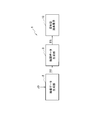
- FIG. 1 is a block diagram showing a phase modulation apparatus according to an embodiment.
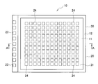
- FIG. 2 is a top view showing an example of a reflective liquid crystal element.
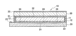
- FIG. 3 is a cross-sectional view of the reflective liquid crystal element cut along the line AA in FIG.
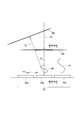
- FIG. 4 is a diagram showing phase modulation of signal light by the reflective liquid crystal element.
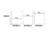
- FIG. 5A is a diagram showing a drive voltage applied to the pixel electrode.
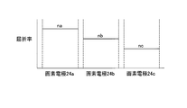
- FIG. 5B is a diagram showing the refractive index of liquid crystal on the pixel electrode.
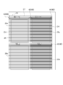
- FIG. 6 is a diagram for explaining the relationship between the pixel block and the blank area.
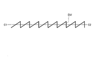
- FIG. 7A is a diagram showing an example of a voltage pattern of drive voltage in B1-B2 of FIG.
- FIG. 7B is a diagram showing an example of a voltage pattern of drive voltages in C1-C2 of FIG.
- the phase modulation device 1 includes an image data generation unit 2, a gradation data generation unit 3, and a reflective liquid crystal element 10.
- the reflective liquid crystal element 10 is, for example, an LCOS element.
- the reflective liquid crystal element 10 is referred to as an LCOS element 10.
- Information data JD is input to the image data generation unit 2.
- the information data JD is a parameter indicating the relationship between the positions of the input and output ports of the signal light and the angle of the reflected light to the incident light in the signal light, and the wavelength band of the signal light, And parameters related to the distribution of the change amount of The amount of change in phase corresponds to the distribution of phase velocity, with the lead or lag of the phase of the reflected light relative to the phase of the incident light.
- the signal light emitted from a predetermined input port is phase-modulated by the phase modulation device 1 and is incident on the target output port.
- the image data generation unit 2 sets the distribution of the phase change amount based on the information data JD.
- the image data generation unit 2 generates the image data DD based on the distribution of the change amount of the phase or the distribution of the phase velocity, and outputs the image data DD to the gradation data generation unit 3.
- the gradation data generation unit 3 generates gradation data DS corresponding to each pixel in the LCOS element 10 of the image data DD, and outputs the gradation data DS to the LCOS element 10 according to the timing of being written to each pixel. A driving voltage corresponding to this gradation is generated in the LCOS element 10 and applied to the liquid crystal.
- the LCOS element 10 includes a drive substrate 20, a transparent substrate 30, a liquid crystal 11, and a sealing material 12.
- the drive substrate 20 has a pixel area 21, an alignment film 22, and a connection terminal 23.
- a plurality of reflective pixel electrodes 24 are arranged in the horizontal direction and the vertical direction.
- One pixel electrode 24 constitutes one pixel.
- the alignment film 22 is formed at least on the pixel region 21.
- the connection terminal 23 is formed at the outer peripheral portion of the drive substrate 20, receives the gradation data DS from the gradation data generation unit 3, and receives a timing control signal from the outside.
- the connection terminal 23 is also connected to a power supply and the like from the outside.
- the transparent substrate 30 has a transparent electrode 31 and an alignment film 32.
- the alignment film 32 is formed on the transparent electrode 31.
- the drive substrate 20 and the transparent substrate 30 are bonded with a gap by a sealing material 12 so that the pixel electrode 24 and the transparent electrode 31 face each other.
- the sealing material 12 is annularly formed along the outer peripheral portion of the pixel area 21.
- the liquid crystal 11 is filled in the gap between the drive substrate 20 and the transparent substrate 30 and sealed by the sealing material 12. You may form the anti-reflective film 33 in the surface on the opposite side to the surface in which the transparent electrode 31 of the transparent substrate 30 is formed.
- a semiconductor substrate for example, a silicon substrate
- a drive circuit for driving each pixel is formed in the drive substrate 20.
- a metal material containing aluminum as its main component can be used as a material of the pixel electrode 24 and the connection terminal 23.
- An alkali-free glass substrate or a quartz glass substrate can be used as the transparent substrate 30.
- ITO Indium Tin Oxide
- a dielectric film may be formed on the upper side and the lower side of the ITO film.
- an ultraviolet curable resin, a thermosetting resin, or a resin that is cured by using ultraviolet light and heat in combination can be used.
- a dielectric multilayer film can be used as the antireflective film 33.
- the pixel block 25 has a configuration in which three or more pixel electrodes 24 are respectively arranged in the horizontal direction and the vertical direction. In order to distinguish each pixel electrode 24, the pixel electrode 24a, the pixel electrode 24b, and the pixel electrode 24c are used from the left.
- the drive voltages DVa, DVb and DVc applied to the liquid crystal 11 are voltages applied between the pixel electrodes 24 a and 24 b and 24 c and the transparent electrode 31. Since the liquid crystal 11 has anisotropy in the refractive index and the dielectric constant of the constituent molecules, the refractive index is changed by changing the inclination of the molecules according to the applied drive voltage.
- the liquid crystal 11 on the pixel electrode 24a has a first refractive index na
- the liquid crystal 11 on the pixel electrode 24b has a second refractive index nb
- the liquid crystal 11 has a third refractive index nc (na> nb> nc).
- the refractive indexes na to nc are average refractive indexes of the liquid crystal 11 on the pixel electrodes 24a to 24c.
- the signal light SL output from the input port enters the pixel block 25 in the state of linear polarization of p polarization or s polarization.
- the alignment films 22 and 32 shown in FIG. 3 are formed such that the deflection direction of the signal light SL and the alignment direction of the liquid crystal 11 are the same.
- the alignment direction is, for example, a direction in which the liquid crystal 11 in the vicinity of the alignment film 22 is inclined.
- the direction in which the liquid crystal 11 in the vicinity of the alignment film 32 is inclined may be the alignment direction.
- the signal light SL By making the polarization direction of the signal light SL the same as the alignment direction of the liquid crystal 11, linearly polarized light is modulated to elliptically polarized light, and p polarized light has s polarized light component or s polarized light has p polarized light component Thus, the signal light SL can be efficiently reflected by suppressing the attenuation of the signal light SL caused by the above.
- Pa, pb and pc shown in FIG. 4 schematically indicate the difference in phase velocity caused by the difference in refractive index of the liquid crystal 11 on the pixel electrodes 24 a, 24 b and 24 c.
- WF shown in FIG. 4 schematically shows the wavefront of the signal light SL.
- the wavefront WF is a surface on which the phases of the signal light SL are aligned.
- the amount of change in phase or phase velocity of the signal light SL gradually increases from the pixel electrode 24 a to the pixel electrode 24 c. Thereby, the wavefront WF of the signal light SL can be changed (tilted).
- the inclination angle ⁇ of the wavefront WF is increased. can do. Further, the inclination angle ⁇ of the wavefront WF can be reduced by reducing the difference in refractive index of the liquid crystal 11 on the pixel electrodes 24 a, 24 b and 24 c and reducing the difference in phase change.
- the inclination angle ⁇ corresponds to the angle between the wavefront WF of the signal light SL and the vertical line of the pixel electrodes 24a, 24b, and 24c.
- the inclination angle ⁇ of the wavefront WF can also be changed by changing the number of pixel electrodes 24.
- the wave front WF of the signal light SL is set to a predetermined inclination angle ⁇ based on the image data DD generated by the image data generation unit 2, and the signal light SL is reflected by the pixel electrodes 24a, 24b, and 24c. Therefore, the LCOS element 10 can reflect the signal light SL in a predetermined direction by changing the phase velocity of the signal light SL stepwise for each pixel based on the image data DD.
- the LCOS element 10 can control the tilt angle ⁇ of the wavefront WF of the signal light SL in accordance with the rate of change of the phase velocity. That is, the LCOS element 10 functions as a phase modulation element that changes the phase velocity for each pixel and reflects the signal light SL in a predetermined direction. The LCOS element 10 controls the tilt angle ⁇ of the wavefront WF of the signal light SL, whereby the signal light SL is incident on the target output port.
- FIG. 6 shows an enlarged upper right portion of the pixel area 21 shown in FIG.
- the pixel area 21 is composed of a plurality of pixel blocks 25. Signal light SL is incident for each pixel block 25.
- the range and position of the pixel block 25 are determined based on the information data JD.
- the pixel block 25 is configured to include an incident region 26 where the signal light SL is incident.
- the incident area 26 is determined based on the spot diameter, the spot shape, and the incident position accuracy of the signal light SL.
- the LCOS element 10 can reconfigure the pixel block 25 in accordance with the change content of the information data JD.
- the LCOS element 10 can control the tilt angle ⁇ of the wavefront WF of the signal light SL for each pixel block 25 based on the image data DD generated by the image data generation unit 2.
- the upper left pixel block 25 in FIG. 6 is the pixel block 25a
- the lower left pixel block 25 is the pixel block 25b
- the upper right pixel block 25 is the pixel block 25c
- the block 25 is a pixel block 25d.
- Signal lights SL of different wavelength bands can be incident on the pixel blocks 25a to 25d.
- the LCOS element 10 can apply drive voltages DV having different voltage patterns to the pixel blocks 25a to 25d based on the image data DD.
- FIG. 7A shows a voltage pattern of the drive voltage DV of successive pixels in B1-B2 of the pixel block 25a shown in FIG.
- FIG. 6 shows the same voltage pattern as the pixel block 25a in the pixel block 25c, the drive voltage DV having a different voltage pattern can be applied.
- FIG. 7B shows a voltage pattern of the drive voltage DV of consecutive pixels in C1-C2 of the pixel block 25c shown in FIG.
- FIG. 6 shows the same voltage pattern as the pixel block 25c in the pixel block 25d, the drive voltage DV having a different voltage pattern can be applied.
- the drive voltage DV has a sawtooth voltage pattern.
- the voltage is continuous for each pixel in actuality, it has a step-like shape, but it is illustrated as a sawtooth shape here.
- Dark portions in the pixel blocks 25a to 25d shown in FIG. 6 correspond to low voltage portions of the voltage pattern of the drive voltage DV shown in FIG. 7A or 7B, and bright portions correspond to high voltage portions.
- the amplitude of the voltage value is larger than that of the voltage pattern shown in FIG. 7A, so the inclination angle ⁇ of the wavefront WF of the signal light SL is large.
- the liquid crystal 11 is assumed to be a liquid crystal material of horizontal alignment, that is, a liquid crystal material having positive dielectric anisotropy.
- the refractive index increases as the voltage amplitude is applied larger.
- a vertically aligned liquid crystal material that is, a liquid crystal material having negative dielectric anisotropy
- increasing the voltage amplitude lowers the refractive index.
- the anisotropy of the refractive index and the refractive index differs depending on the liquid crystal material.
- the amount of change in phase obtained varies depending on the thickness of the liquid crystal layer.
- the voltage pattern of the drive voltage DV is set based on the image data DD generated by the image data generation unit 2. Therefore, the range and position of the pixel blocks 25a to 25d are determined based on the information data JD, and the incident signal light SL is phase-modulated based on the voltage pattern of the drive voltage DV to change the wavefront WF of the signal light SL. It can be (tilted). Note that control by a PWM method in which the drive voltage DV is controlled by the pulse width or the number of pulses is also effective. In this case, the vertical axis in FIGS. 7A and 7B corresponds to the integration time of the application pulse of the drive voltage DV in one frame.
- blank areas 40 which do not contribute to phase modulation are formed between the pixel blocks 25 and in the outer peripheral area 27 of the pixel area 21.
- the blank area 40 formed between the pixel blocks 25 in the first direction (vertical direction in FIG. 6) in which the sawtooth wave voltage pattern is repeated is orthogonal to the blank area 41 (first blank area) in the first direction.
- the blank area 40 formed between the pixel blocks 25 in the second direction (the left and right direction in FIG. 6) is referred to as a blank area 42 (second blank area).
- the blank area 40 formed adjacent to the pixel block 25 in the outer peripheral area 27 of the pixel area 21 in the first direction is a blank area 43 (third blank area), and the outer peripheral area 27 of the pixel area 21 in the second direction.
- the blank area 40 formed adjacent to the pixel block 25 is referred to as a blank area 44 (fourth blank area).
- the blank area 41 is adjacent to the pixel blocks 25a and 25b and adjacent to the pixel blocks 25c and 25d. In the blank area 41, two or more pixel electrodes 24 are arranged in the first direction.
- the drive voltage DV having the same voltage value or pulse width as the drive voltage DV applied to the pixel electrode 24 of the pixel block 25a is applied to the pixel electrode 24 of the blank area 41 adjacent to the pixel electrode 24 of the pixel block 25a.
- the drive voltage DV having the same voltage value or pulse width as the drive voltage DV applied to the pixel electrode 24 of the pixel block 25b is applied to the pixel electrode 24 of the blank area 41 adjacent to the pixel electrode 24 of the pixel block 25b.
- the voltage value of the drive voltage DV applied to the pixel electrode 24 of the pixel block 25a is va
- the voltage value of the drive voltage DV applied to the pixel electrode 24 of the pixel block 25b is vb (va> vb).
- the driving voltage DV of voltage value va is applied to the pixel electrode 24 of the blank area 41 adjacent to the pixel electrode 24 of the pixel block 25a, and the voltage is applied to the pixel electrode 24 of the blank area 41 adjacent to the pixel electrode 24 of the pixel block 25b.
- a drive voltage DV of value vb is applied.
- the relationship between the drive voltage DV of the pixel blocks 25 c and 25 d and the blank area 41 is similar to the relationship of the drive voltage DV between the pixel blocks 25 a and 25 b and the blank area 41.
- the blank area 42 is adjacent to the pixel blocks 25a and 25c and adjacent to the pixel blocks 25b and 25d.
- two or more, preferably four or more pixel electrodes 24 are arranged in the second direction.
- the drive voltage DV having the same voltage pattern as that of the adjacent pixel block 25 is applied to the blank area 42.
- the drive voltage DV having the same voltage value or pulse width as the drive voltage DV applied to the pixel electrode 24 of the pixel block 25a is applied.
- the drive voltage DV having the same voltage value or pulse width as the drive voltage DV applied to the pixel electrode 24 of the pixel block 25c is applied to the pixel electrode 24 of the blank area 42 adjacent to the pixel electrode 24 of the pixel block 25c. Ru.
- the relationship between the drive voltage DV for the pixel blocks 25b and 25d and the blank area 42 is the same as the relationship between the drive voltage DV for the pixel blocks 25a and 25c and the blank area 42.
- the blank area 43 is adjacent to the pixel blocks 25a and 25c. In the blank area 43, one or more, preferably two or more pixel electrodes 24 are disposed in the first direction.
- the drive voltage DV having the same voltage value or pulse width as the drive voltage DV applied to the pixel electrode 24 of the pixel block 25a is applied to the pixel electrode 24 of the blank area 43 adjacent to the pixel electrode 24 of the pixel block 25a.
- the voltage value of the drive voltage DV applied to the pixel electrode 24 of the pixel block 25a adjacent to the blank area 43 is vc
- the voltage is applied to the pixel electrode 24 of the blank area 43 adjacent to the pixel electrode 24 of the pixel block 25a.
- a drive voltage DV of value vc is applied.
- the relationship between the drive voltage DV of the pixel block 25 c and the blank area 43 is the same as the relationship of the drive voltage DV between the pixel block 25 a and the blank area 43.
- the blank area 44 is adjacent to the pixel blocks 25c and 25d.
- one or more, preferably two or more pixel electrodes 24 are disposed in the second direction.
- the drive voltage DV having the same voltage pattern as that of the adjacent pixel block 25 is applied to the blank area 44.
- the drive voltage DV having the same voltage value or pulse width as the drive voltage DV applied to the pixel electrode 24 of the pixel block 25c. Is applied.
- the relationship between the drive voltage DV between the pixel block 25 d and the blank area 44 is the same as the relationship between the drive voltage DV between the pixel block 25 c and the blank area 44.
- the occurrence of disclination caused by the potential difference between the pixels of the pixel block 25 and the blank area 40 can be suppressed.
- phase modulation device 1 of the present embodiment two or more pixel electrodes 24 are disposed in the first direction in the blank area 41, and two or more pixel electrodes 24 are disposed in the second direction in the blank area 42. It has composition. Furthermore, in the phase modulation device 1, the blank area 43 has one or more pixel electrodes 24 arranged in the first direction, and the blank area 44 has one or more pixel electrodes 24 arranged in the second direction. Have. The arrangement number of the pixel electrodes 24 in each of the above-mentioned blank areas 40 is appropriately set based on the information data JD so as to suppress the occurrence of disclination.
Landscapes
- Physics & Mathematics (AREA)
- Nonlinear Science (AREA)
- General Physics & Mathematics (AREA)
- Optics & Photonics (AREA)
- Chemical & Material Sciences (AREA)
- Crystallography & Structural Chemistry (AREA)
- Mathematical Physics (AREA)
- Engineering & Computer Science (AREA)
- Computer Hardware Design (AREA)
- Theoretical Computer Science (AREA)
- Geometry (AREA)
- Liquid Crystal (AREA)
- Microelectronics & Electronic Packaging (AREA)
- Optical Modulation, Optical Deflection, Nonlinear Optics, Optical Demodulation, Optical Logic Elements (AREA)
Abstract
位相変調装置(1)は画像データ生成部(2)と階調データ生成部(3)と画素領域(21)を有する反射型液晶素子(10)とを備える。画素領域(21)は複数の画素ブロック(25)と、ブランクエリア(41)とを有する。画像データ生成部(2)は情報データ(JD)に基づいて位相の変化量の分布または位相速度の分布に対応する画像データ(DD)を生成する。階調データ生成部(3)は画像データ(DD)に基づいて各画素に対応する階調データ(DS)を生成する。画素ブロック(25)は階調データ(DS)に対応する電圧パターンの駆動電圧(DV)に基づいて信号光(SL)の波面(WF)を変化させる。ブランクエリア(41)は、画素ブロック(25)の画素電極(24)と隣り合う画素電極(24)に同じ駆動電圧が印加される。
Description
本開示は、液晶素子を用いた位相変調装置に関する。
近年、光通信分野では激増する情報量に対応するため、環状に形成された光ネットワークシステム、及び、光波長多重通信システムが提唱されている。これら光通信システムにおける光信号の分岐または挿入を、電気信号への変換を中継することなく実行できるROADM(Reconfigurable Optical And Drop Multiplexer)装置が用いられ、その中で光スイッチング装置としてWSS(Wavelength Selective Switch)装置が用いられる。WSS装置における光スイッチング素子として、MEMS(Micro Electro Mechanical Systems)ミラー、及び、反射型液晶素子、例えばLCOS(Liquid Crystal on Silicon)素子等が用いられる。
LCOS素子は、複数の反射型の画素電極が水平方向、及び、垂直方向に配置されている画素領域を有する反射型液晶素子である。各画素電極上の液晶の屈折率は、液晶に印加される電圧を画素電極ごとに制御することにより変化する。信号光の位相速度は、各画素上の液晶の屈折率を変化させることにより、画素ごとに制御される。
LCOS素子は、位相速度を画素ごとに段階的に変化させることにより、信号光の波面を傾斜させることができる。LCOS素子は、信号光の波面の傾斜角を位相速度の変化の割合に応じて制御することができる。即ち、LCOS素子は、画素ごとに位相速度を変化させて信号光を所定の方向に反射する位相変調素子として機能する。
MEMSミラーは信号光の波長帯の数に対応してミラーが必要になる。そのため、信号光の波長帯またはその数を変更する場合、変更内容に対応させてMEMSミラーを新たに作製しなければならない。
それに対して、LCOS素子は画素領域を複数の画素ブロックに任意に分割し、画素ブロックごとに制御することができる。そのため、信号光の波長帯またはその数を変更する場合、変更内容に対応させて画素ブロックを再構成することができるので、液晶素子を新たに作製する必要がない。即ち、LCOS素子は、MEMSミラーよりも可変グリッド性に優れている。特許文献1には、LCOS素子を用いた位相変調装置の一例が記載されている。
LCOS素子には画素ブロックごとに信号光が照射される。通常、画素ブロック間には位相変調に寄与しないブランクエリアが形成される。画素ブロックとブランクエリアとの画素間の電位差に起因してディスクリネーションが発生する場合がある。ディスクリネーションとは、隣り合う画素間の電位差に起因して液晶分子が意図した方向とは異なる方向に傾斜することである。画素間の電位差が大きいと横電界が大きくなるため、ディスクリネーションが発生しやすくなったり、発生領域が広がったりする。
信号光はディスクリネーションの影響により、目的の傾斜角とは異なる傾斜角で反射されてしまうため、目的の出力ポートとは異なる出力ポートに入射するクロストークが発生する。
実施形態は、画素ブロックとブランクエリアとの画素間の電位差に起因するディスクリネーションの発生を抑制する位相変調装置を提供することを目的とする。
実施形態の一態様によれば、情報データに基づいて位相の変化量の分布または位相速度の分布に対応する画像データを生成する画像データ生成部と、前記画像データに基づいて各画素に対応する階調データを生成する階調データ生成部と、複数の画素電極が配置され、前記階調データに対応する鋸歯状波の電圧パターンの駆動電圧が印加される画素領域を有する反射型液晶素子とを備え、前記画素領域は、入射される信号光を前記電圧パターンに基づいて位相変調させ、前記信号光の波面を変化させる複数の画素ブロックと、前記電圧パターンが繰り返される第1の方向における画素ブロック間に形成された第1のブランクエリアとを有し、前記第1のブランクエリアは、前記第1の方向に2個以上の画素電極が配置され、前記画素ブロックの画素電極と隣り合う画素電極には、前記画素ブロックの画素電極に印加される駆動電圧と同じ駆動電圧が印加されることを特徴とする位相変調装置が提供される。
実施形態の位相変調装置によれば、画素ブロックとブランクエリアとの画素間の電位差に起因するディスクリネーションの発生を抑制できる。
図1を用いて、一実施形態の位相変調装置を説明する。位相変調装置1は、画像データ生成部2と、階調データ生成部3と、反射型液晶素子10とを備える。反射型液晶素子10は例えばLCOS素子である。以下、反射型液晶素子10をLCOS素子10とする。
画像データ生成部2には情報データJDが入力される。情報データJDは、信号光の入力ポート及び出力ポートの位置と信号光における入射光に対する反射光の角度との関係を示すパラメータと、信号光の波長帯、即ち所望の反射光角度を実現する位相の変化量の分布に関わるパラメータとを含む。位相の変化量は、入射光の位相に対する反射光の位相の進みまたは遅れで、位相速度の分布に対応する。所定の入力ポートから射出された信号光は、位相変調装置1により位相変調されて目的の出力ポートへ入射する。
画像データ生成部2は、情報データJDに基づいて位相の変化量の分布を設定する。画像データ生成部2は、位相の変化量の分布、または、位相速度の分布に基づいて画像データDDを生成し、階調データ生成部3へ出力する。階調データ生成部3は、画像データDDのLCOS素子10における各画素に対応する階調データDSを生成し、各画素に書き込まれるタイミングに合わせてLCOS素子10へ出力する。この階調に対応する駆動電圧がLCOS素子10内で生成され、液晶に印加される。
図2または図3を用いて、LCOS素子10の構成例を説明する。LCOS素子10は、駆動基板20と、透明基板30と、液晶11と、シール材12とを有する。駆動基板20は、画素領域21と、配向膜22と、接続端子23とを有する。
画素領域21には、複数の反射型の画素電極24が水平方向及び垂直方向に配置されている。1個の画素電極24が1画素を構成する。配向膜22は少なくとも画素領域21上に形成されている。接続端子23は、駆動基板20の外周部に形成され、階調データ生成部3から階調データDSが入力され、外部からタイミング制御信号が入力される。また、接続端子23は外部から電源等も接続されている。
透明基板30は、透明電極31と、配向膜32とを有する。配向膜32は透明電極31上に形成されている。駆動基板20と透明基板30とは、画素電極24と透明電極31とが対向するようにシール材12により間隙を有して接着されている。
シール材12は画素領域21の外周部に沿って環状に形成されている。液晶11は、駆動基板20と透明基板30との間隙に充填され、シール材12により封止されている。透明基板30の透明電極31が形成されている面とは反対側の面に反射防止膜33を形成してもよい。
駆動基板20として半導体基板(例えばシリコン基板)を用いることができる。なお、駆動基板20には、各画素を駆動するための駆動回路が形成されている。画素電極24、及び、接続端子23の材料としてアルミニウムを主成分とする金属材料を用いることができる。
透明基板30として無アルカリガラス基板または石英ガラス基板を用いることができる。透明電極31の材料としてITO(Indium Tin Oxide)を用いることができる。なお、ITO膜の上側及び下側に誘電体膜を形成してもよい。シール材12として紫外線硬化性樹脂、熱硬化性樹脂、または紫外線と熱との併用により硬化する樹脂を用いることができる。反射防止膜33として誘電体多層膜を用いることができる。
図4、図5A、及び、図5Bを用いて、LCOS素子10による信号光の位相変調を説明する。説明を分かりやすくするために、3個の画素電極24により画素ブロック25を構成する場合について説明する。通常、画素ブロック25は、3個以上の画素電極24が水平方向及び垂直方向にそれぞれ配置されている構成を有する。各画素電極24を区別するため、左から画素電極24a、画素電極24b、及び、画素電極24cとする。
図1に示す画像データ生成部2により生成された位相の変化量の分布(位相速度の分布)に応じた画像データDDに基づいて、図5Aに示すように、画素電極24a、24b、及び、24cには異なる駆動電圧DVa、DVb、及び、DVcが印加される。実際には、液晶11に印加される駆動電圧DVa、DVb、及び、DVcは、画素電極24a、24b、及び、24cと透明電極31との間に加わる電圧である。液晶11は、構成される分子の屈折率と誘電率に異方性を有することから、印加される駆動電圧によって分子の傾斜が変化することで屈折率が変化する。
これにより、図5Bに示すように、画素電極24a上の液晶11は第1の屈折率naを有し、画素電極24b上の液晶11は第2の屈折率nbを有し、画素電極24c上の液晶11は第3の屈折率nc(na>nb>nc)を有する。屈折率na~ncは画素電極24a~24c上の液晶11の平均的な屈折率である。
入力ポートから出力された信号光SLは、p偏光またはs偏光の直線偏光の状態で画素ブロック25に入射する。図3に示す配向膜22及び32は、信号光SLの偏向方向と液晶11の配向方向とが同じになるように形成されている。配向方向とは、例えば配向膜22付近の液晶11が傾斜する方向である。なお、配向膜32付近の液晶11が傾斜する方向を配向方向としてもよい。
信号光SLの偏向方向と液晶11の配向方向とを同じにすることにより、直線偏光が楕円偏光へと変調されて、p偏光がs偏光成分を有する、または、s偏光がp偏光成分を有することによって生じる信号光SLの減衰を抑制して、信号光SLを効率的に反射させることができる。
図4に示すpa、pb、及び、pcは、画素電極24a、24b、及び、24c上の液晶11の屈折率の違いにより生じる位相速度の違いを模式的に示している。図4に示すWFは信号光SLの波面を模式的に示している。波面WFは、信号光SLの位相が揃った面をいう。信号光SLは、画素電極24aから画素電極24cに向かって位相の変化量または位相速度が段階的に大きくなる。これにより、信号光SLの波面WFを変化(傾斜)させることができる。
駆動電圧DVa、DVb、及び、DVcにより、画素電極24a、24b、及び、24c上の液晶11の屈折率の差を大きくし、位相変化の差を大きくすることで波面WFの傾斜角θを大きくすることができる。また、画素電極24a、24b、及び、24c上の液晶11の屈折率の差を小さくし、位相変化の差を小さくすることで波面WFの傾斜角θを小さくすることができる。傾斜角θは、信号光SLの波面WFと画素電極24a、24b、及び、24cの垂線とのなす角度に相当する。なお、画素電極24の数を変えることにより波面WFの傾斜角θを変化させることもできる。
信号光SLは、画像データ生成部2により生成された画像データDDに基づいて、波面WFが所定の傾斜角θとされ、画素電極24a、24b、及び、24cにより反射される。従って、LCOS素子10は、画像データDDに基づいて、信号光SLの位相速度を画素ごとに段階的に変化させることにより、信号光SLを所定の方向に反射させることができる。
LCOS素子10は、信号光SLの波面WFの傾斜角θを位相速度の変化の割合に応じて制御することができる。即ち、LCOS素子10は、画素ごとに位相速度を変化させて信号光SLを所定の方向に反射する位相変調素子として機能する。LCOS素子10が信号光SLの波面WFの傾斜角θを制御することにより、信号光SLは目的の出力ポートに入射される。
図6、図7A、及び、図7Bを用いて、画素領域21における画素ブロックとブランクエリアとの関係を説明する。図6は、図2に示す画素領域21の右上部分を拡大して示している。画素領域21は、複数の画素ブロック25により構成される。信号光SLは画素ブロック25ごとに入射される。
画素ブロック25は、情報データJDに基づいて範囲及び位置が決定される。画素ブロック25は信号光SLが入射される入射領域26を含むように構成されている。入射領域26は、信号光SLのスポット径、スポット形状、及び入射位置精度等に基づいて決定される。LCOS素子10は、情報データJDの変更内容に対応させて画素ブロック25を再構成することができる。
LCOS素子10は、画像データ生成部2により生成される画像データDDに基づいて、画素ブロック25ごとに信号光SLの波面WFの傾斜角θを制御することができる。各画素ブロック25を区別するため、図6における左上側の画素ブロック25を画素ブロック25a、左下側の画素ブロック25を画素ブロック25b、右上側の画素ブロック25を画素ブロック25c、右下側の画素ブロック25を画素ブロック25dとする。
画素ブロック25a~25dには、異なる波長帯の信号光SLを入射させることができる。LCOS素子10は、画像データDDに基づいて、画素ブロック25a~25dに異なる電圧パターンの駆動電圧DVを印加させることができる。
図7A及び図7Bを用いて、駆動電圧DVを電圧値の振幅で制御する場合について説明する。図7Aは、図6に示す画素ブロック25aのB1-B2における連続した画素の駆動電圧DVの電圧パターンを示している。なお、図6では画素ブロック25cには画素ブロック25aと同じ電圧パターンを示しているが、異なる電圧パターンの駆動電圧DVを印加させることができる。
図7Bは、図6に示す画素ブロック25cのC1-C2における連続した画素の駆動電圧DVの電圧パターンを示している。なお、図6では画素ブロック25dには画素ブロック25cと同じ電圧パターンを示しているが、異なる電圧パターンの駆動電圧DVを印加させることができる。
図7A及び図7Bに示すように、駆動電圧DVは鋸歯状波の電圧パターンを有する。なお、実際には連続した画素ごとの電圧なので階段状になるが、ここでは鋸歯状に図示する。図6に示す画素ブロック25a~25dにおいて暗い部分は、図7Aまたは図7Bに示す駆動電圧DVの電圧パターンの電圧の低い部分に相当し、明るい部分は電圧の高い部分に相当する。図7Bに示す電圧パターンは、図7Aに示す電圧パターンよりも電圧値の振幅が大きいため、信号光SLの波面WFの傾斜角θは大きくなる。
ここでは、液晶11は、水平配向の液晶材料、即ち正の誘電率異方性を有する液晶材料を想定している。水平配向の液晶では、電圧振幅をより大きく印加するほど屈折率が高くなる。垂直配向の液晶材料、即ち負の誘電率異方性を有する液晶材料の場合、電圧振幅を大きくすることで屈折率は低くなる。また、液晶材料によって屈折率及び屈折率の異方性が異なる。加えて、液晶層の厚みによっても結果的に得られる位相の変化量は異なる。
駆動電圧DVの電圧パターンは、画像データ生成部2により生成された画像データDDに基づいて設定される。従って、画素ブロック25a~25dは、情報データJDに基づいて範囲及び位置が決定され、入射される信号光SLを駆動電圧DVの電圧パターンに基づいて位相変調させ、信号光SLの波面WFを変化(傾斜)させることができる。なお、駆動電圧DVをパルス幅またはパルスの数で制御するPWM方式による制御も有効である。この場合、図7A及び図7Bにおける縦軸は、1フレームにおける駆動電圧DVの印加パルスの積算時間に相当する。
図6に示すように、通常、画素ブロック25間、及び、画素領域21の外周領域27には、位相変調に寄与しないブランクエリア40が形成される。鋸歯状波の電圧パターンが繰り返される第1の方向(図6の上下方向)における画素ブロック25間に形成されるブランクエリア40をブランクエリア41(第1のブランクエリア)、第1の方向に直交する第2の方向(図6の左右方向)における画素ブロック25間に形成されるブランクエリア40をブランクエリア42(第2のブランクエリア)とする。
第1の方向における画素領域21の外周領域27に画素ブロック25に隣接して形成されるブランクエリア40をブランクエリア43(第3のブランクエリア)、第2の方向における画素領域21の外周領域27に画素ブロック25に隣接して形成されるブランクエリア40をブランクエリア44(第4のブランクエリア)とする。
ブランクエリア41は、画素ブロック25a及び25bと隣接し、画素ブロック25c及び25dと隣接している。ブランクエリア41は、第1の方向に2個以上の画素電極24が配置されている。画素ブロック25aの画素電極24と隣り合うブランクエリア41の画素電極24には、画素ブロック25aの画素電極24に印加される駆動電圧DVと同じ電圧値またはパルス幅の駆動電圧DVが印加される。
画素ブロック25bの画素電極24と隣り合うブランクエリア41の画素電極24には、画素ブロック25bの画素電極24に印加される駆動電圧DVと同じ電圧値またはパルス幅の駆動電圧DVが印加される。
例えば、画素ブロック25aの画素電極24に印加される駆動電圧DVの電圧値をva、画素ブロック25bの画素電極24に印加される駆動電圧DVの電圧値をvb(va>vb)とする。画素ブロック25aの画素電極24と隣り合うブランクエリア41の画素電極24には電圧値vaの駆動電圧DVが印加され、画素ブロック25bの画素電極24と隣り合うブランクエリア41の画素電極24には電圧値vbの駆動電圧DVが印加される。
従って、画素ブロック25a及び25bとブランクエリア41との電位差を低減することができるので、ディスクリネーションの発生を抑制できる。なお、画素ブロック25c及び25dとブランクエリア41との駆動電圧DVの関係は、画素ブロック25a及び25bとブランクエリア41との駆動電圧DVの関係と同様である。
ブランクエリア42は、画素ブロック25a及び25cと隣接し、画素ブロック25b及び25dと隣接している。ブランクエリア42は、第2の方向に2個以上、好ましくは4個以上の画素電極24が配置されている。ブランクエリア42は、隣接する画素ブロック25と同じ電圧パターンの駆動電圧DVが印加される。
具体的には、画素ブロック25aの画素電極24と隣り合うブランクエリア42の画素電極24には、画素ブロック25aの画素電極24に印加される駆動電圧DVと同じ電圧値またはパルス幅の駆動電圧DVが印加される。また、画素ブロック25cの画素電極24と隣り合うブランクエリア42の画素電極24には、画素ブロック25cの画素電極24に印加される駆動電圧DVと同じ電圧値またはパルス幅の駆動電圧DVが印加される。
従って、画素ブロック25a及び25cとブランクエリア42との電位差を低減することができるので、ディスクリネーションの発生を抑制できる。なお、画素ブロック25b及び25dとブランクエリア42との駆動電圧DVの関係は、画素ブロック25a及び25cとブランクエリア42との駆動電圧DVの関係と同様である。
ブランクエリア43は、画素ブロック25a及び25cと隣接している。ブランクエリア43は、第1の方向に1個以上、好ましくは2個以上の画素電極24が配置されている。画素ブロック25aの画素電極24と隣り合うブランクエリア43の画素電極24には、画素ブロック25aの画素電極24に印加される駆動電圧DVと同じ電圧値またはパルス幅の駆動電圧DVが印加される。
例えば、ブランクエリア43に隣接する画素ブロック25aの画素電極24に印加される駆動電圧DVの電圧値をvcとすると、画素ブロック25aの画素電極24と隣り合うブランクエリア43の画素電極24には電圧値vcの駆動電圧DVが印加される。
従って、画素ブロック25aとブランクエリア43との電位差を低減することができるので、ディスクリネーションの発生を抑制できる。なお、画素ブロック25cとブランクエリア43との駆動電圧DVの関係は、画素ブロック25aとブランクエリア43との駆動電圧DVの関係と同様である。
ブランクエリア44は、画素ブロック25c及び25dと隣接している。ブランクエリア44は、第2の方向に1個以上、好ましくは2個以上の画素電極24が配置されている。ブランクエリア44は、隣接する画素ブロック25と同じ電圧パターンの駆動電圧DVが印加される。具体的には、画素ブロック25cの画素電極24と隣り合うブランクエリア44の画素電極24には、画素ブロック25cの画素電極24に印加される駆動電圧DVと同じ電圧値またはパルス幅の駆動電圧DVが印加される。
従って、画素ブロック25cとブランクエリア44との電位差を低減することができるので、ディスクリネーションの発生を抑制できる。なお、画素ブロック25dとブランクエリア44との駆動電圧DVの関係は、画素ブロック25cとブランクエリア44との駆動電圧DVの関係と同様である。
本実施形態の位相変調装置1によれば、画素ブロック25の画素電極24と隣り合うブランクエリア40の画素電極24に、画素ブロック25の画素電極24に印加される駆動電圧DVと同じ電圧値またはパルス幅の駆動電圧DVが印加される。これにより、画素ブロック25とブランクエリア40との画素間の電位差に起因するディスクリネーションの発生を抑制できる。
本発明は、上述した本実施形態に限定されるものではなく、本発明の要旨を逸脱しない範囲において種々変更可能である。
本実施形態の位相変調装置1では、ブランクエリア41は第1の方向に2個以上の画素電極24が配置され、ブランクエリア42は第2の方向に2個以上の画素電極24が配置される構成を有する。さらに、位相変調装置1では、ブランクエリア43は第1の方向に1個以上の画素電極24が配置され、ブランクエリア44は第2の方向に1個以上の画素電極24が配置される構成を有する。上記の各ブランクエリア40における画素電極24の配置数は、ディスクリネーションの発生を抑制できるように、情報データJDに基づいて適宜設定されるものである。
本願の開示は、2017年10月11日に出願された特願2017-197402号に記載の主題と関連しており、それらの全ての開示内容は引用によりここに援用される。
Claims (5)
- 情報データに基づいて位相の変化量の分布または位相速度の分布に対応する画像データを生成する画像データ生成部と、
前記画像データに基づいて各画素に対応する階調データを生成する階調データ生成部と、
複数の画素電極が配置され、前記階調データに対応する鋸歯状波の電圧パターンの駆動電圧が印加される画素領域を有する反射型液晶素子と、
を備え、
前記画素領域は、
入射される信号光を前記電圧パターンに基づいて位相変調させ、前記信号光の波面を変化させる複数の画素ブロックと、
前記電圧パターンが繰り返される第1の方向における画素ブロック間に形成された第1のブランクエリアと、
を有し、
前記第1のブランクエリアは、前記第1の方向に2個以上の画素電極が配置され、前記画素ブロックの画素電極と隣り合う画素電極には、前記画素ブロックの画素電極に印加される駆動電圧と同じ駆動電圧が印加されることを特徴とする位相変調装置。 - 前記画素領域は、前記第1の方向に直交する第2の方向における画素ブロック間に形成された第2のブランクエリアをさらに有し、
前記第2のブランクエリアは、前記第2の方向に2個以上の画素電極が配置され、前記画素ブロックの画素電極と隣り合う画素電極には、前記画素ブロックの画素電極に印加される駆動電圧と同じ駆動電圧が印加されることを特徴とする請求項1に記載の位相変調装置。 - 前記画素領域は、
前記第1の方向における前記画素領域の外周領域に前記画素ブロックに隣接して形成された第3のブランクエリアをさらに有し、
前記第3のブランクエリアは、前記画素ブロックの画素電極と隣り合う画素電極には、前記画素ブロックの画素電極に印加される駆動電圧と同じ駆動電圧が印加されることを特徴とする請求項1または2に記載の位相変調装置。 - 前記第2の方向における前記画素領域の外周領域に前記画素ブロックに隣接して形成された第4のブランクエリアをさらに有し、
前記第4のブランクエリアは、前記画素ブロックの画素電極と隣り合う画素電極には、前記画素ブロックの画素電極に印加される駆動電圧と同じ駆動電圧が印加されることを特徴とする請求項2に記載の位相変調装置。 - 前記情報データは、前記信号光の入力ポート及び出力ポートの位置と前記信号光における入射光に対する反射光の角度との関係を示すパラメータと、前記信号光の波長帯のパラメータとを含むことを特徴とする請求項1~4のうちのいずれか1項に記載の位相変調装置。
Priority Applications (3)
| Application Number | Priority Date | Filing Date | Title |
|---|---|---|---|
| EP18866691.1A EP3696599B1 (en) | 2017-10-11 | 2018-10-04 | Phase modulation device |
| CN201880065528.3A CN111201481B (zh) | 2017-10-11 | 2018-10-04 | 相位调制装置 |
| US16/842,026 US10838251B2 (en) | 2017-10-11 | 2020-04-07 | Phase modulation device |
Applications Claiming Priority (2)
| Application Number | Priority Date | Filing Date | Title |
|---|---|---|---|
| JP2017197402A JP6791088B2 (ja) | 2017-10-11 | 2017-10-11 | 位相変調装置 |
| JP2017-197402 | 2017-10-11 |
Related Child Applications (1)
| Application Number | Title | Priority Date | Filing Date |
|---|---|---|---|
| US16/842,026 Continuation US10838251B2 (en) | 2017-10-11 | 2020-04-07 | Phase modulation device |
Publications (1)
| Publication Number | Publication Date |
|---|---|
| WO2019073896A1 true WO2019073896A1 (ja) | 2019-04-18 |
Family
ID=66100734
Family Applications (1)
| Application Number | Title | Priority Date | Filing Date |
|---|---|---|---|
| PCT/JP2018/037206 Ceased WO2019073896A1 (ja) | 2017-10-11 | 2018-10-04 | 位相変調装置 |
Country Status (5)
| Country | Link |
|---|---|
| US (1) | US10838251B2 (ja) |
| EP (1) | EP3696599B1 (ja) |
| JP (1) | JP6791088B2 (ja) |
| CN (1) | CN111201481B (ja) |
| WO (1) | WO2019073896A1 (ja) |
Cited By (2)
| Publication number | Priority date | Publication date | Assignee | Title |
|---|---|---|---|---|
| CN110600462A (zh) * | 2019-09-29 | 2019-12-20 | 南京芯视元电子有限公司 | 一种具有多个像素区的系统封装lcos芯片及其应用 |
| CN113495377A (zh) * | 2020-04-08 | 2021-10-12 | 华为技术有限公司 | 硅基液晶加载装置、硅基液晶器件和硅基液晶调制方法 |
Families Citing this family (2)
| Publication number | Priority date | Publication date | Assignee | Title |
|---|---|---|---|---|
| CN114153033B (zh) * | 2020-09-07 | 2026-03-13 | 华为技术有限公司 | 波长选择的方法和装置 |
| CN112596269A (zh) * | 2020-12-18 | 2021-04-02 | 深圳视为光电科技有限公司 | 一种可调控液体透镜镜片、光学视力矫正眼镜及其控制方法 |
Citations (5)
| Publication number | Priority date | Publication date | Assignee | Title |
|---|---|---|---|---|
| JP2007003981A (ja) * | 2005-06-27 | 2007-01-11 | Seiko Epson Corp | 電気光学装置及びその駆動方法並びに電子機器 |
| JP2016122061A (ja) * | 2014-12-24 | 2016-07-07 | 日本電信電話株式会社 | 空間位相変調器 |
| JP2016143037A (ja) | 2015-02-05 | 2016-08-08 | 日本電信電話株式会社 | 空間位相変調器 |
| JP2017054004A (ja) * | 2015-09-09 | 2017-03-16 | 日本電信電話株式会社 | 波長選択スイッチ |
| JP2017197402A (ja) | 2016-04-27 | 2017-11-02 | 株式会社フジクラ | ガラス母材の製造方法及び製造装置 |
Family Cites Families (11)
| Publication number | Priority date | Publication date | Assignee | Title |
|---|---|---|---|---|
| US5815134A (en) * | 1994-05-16 | 1998-09-29 | Semiconductor Energy Laboratory Co., Ltd. | Liquid crystal electro-optical device and driving method thereof |
| JPH10142605A (ja) * | 1996-11-13 | 1998-05-29 | Victor Co Of Japan Ltd | 投射型液晶表示装置 |
| JP4799505B2 (ja) * | 2007-08-03 | 2011-10-26 | 株式会社 日立ディスプレイズ | 液晶表示装置 |
| JP2010151948A (ja) * | 2008-12-24 | 2010-07-08 | Hamamatsu Photonics Kk | 光制御装置および光制御方法 |
| EP2446326A2 (de) * | 2009-06-23 | 2012-05-02 | SeeReal Technologies S.A. | Lichtmodulationsvorrichtung für ein display zur darstellung zwei- und/oder dreidimensionaler bildinhalte mit variablen beugungselementen basierend auf linearen, parallelen elektroden |
| JP5929538B2 (ja) * | 2012-06-18 | 2016-06-08 | セイコーエプソン株式会社 | 表示制御回路、表示制御方法、電気光学装置及び電子機器 |
| WO2014196064A1 (ja) * | 2013-06-06 | 2014-12-11 | 住友電気工業株式会社 | 波長選択スイッチ、および位相変調素子の制御方法 |
| JP5852198B1 (ja) * | 2014-09-11 | 2016-02-03 | 日本電信電話株式会社 | 光入出力装置およびその制御方法 |
| JP6717972B2 (ja) * | 2016-11-29 | 2020-07-08 | シャープ株式会社 | 液晶装置、液晶装置の残留dc電圧値を求める方法、液晶装置の駆動方法、および液晶装置の製造方法 |
| US10505656B2 (en) * | 2017-04-08 | 2019-12-10 | Nokia Solutions And Networks Oy | Optical wavelength selective switches with guard bands |
| JP6555304B2 (ja) * | 2017-07-31 | 2019-08-07 | セイコーエプソン株式会社 | 液晶表示装置および電子機器 |
-
2017
- 2017-10-11 JP JP2017197402A patent/JP6791088B2/ja active Active
-
2018
- 2018-10-04 EP EP18866691.1A patent/EP3696599B1/en active Active
- 2018-10-04 CN CN201880065528.3A patent/CN111201481B/zh active Active
- 2018-10-04 WO PCT/JP2018/037206 patent/WO2019073896A1/ja not_active Ceased
-
2020
- 2020-04-07 US US16/842,026 patent/US10838251B2/en active Active
Patent Citations (5)
| Publication number | Priority date | Publication date | Assignee | Title |
|---|---|---|---|---|
| JP2007003981A (ja) * | 2005-06-27 | 2007-01-11 | Seiko Epson Corp | 電気光学装置及びその駆動方法並びに電子機器 |
| JP2016122061A (ja) * | 2014-12-24 | 2016-07-07 | 日本電信電話株式会社 | 空間位相変調器 |
| JP2016143037A (ja) | 2015-02-05 | 2016-08-08 | 日本電信電話株式会社 | 空間位相変調器 |
| JP2017054004A (ja) * | 2015-09-09 | 2017-03-16 | 日本電信電話株式会社 | 波長選択スイッチ |
| JP2017197402A (ja) | 2016-04-27 | 2017-11-02 | 株式会社フジクラ | ガラス母材の製造方法及び製造装置 |
Non-Patent Citations (1)
| Title |
|---|
| See also references of EP3696599A4 |
Cited By (2)
| Publication number | Priority date | Publication date | Assignee | Title |
|---|---|---|---|---|
| CN110600462A (zh) * | 2019-09-29 | 2019-12-20 | 南京芯视元电子有限公司 | 一种具有多个像素区的系统封装lcos芯片及其应用 |
| CN113495377A (zh) * | 2020-04-08 | 2021-10-12 | 华为技术有限公司 | 硅基液晶加载装置、硅基液晶器件和硅基液晶调制方法 |
Also Published As
| Publication number | Publication date |
|---|---|
| EP3696599A1 (en) | 2020-08-19 |
| JP6791088B2 (ja) | 2020-11-25 |
| CN111201481B (zh) | 2022-08-30 |
| US20200233262A1 (en) | 2020-07-23 |
| US10838251B2 (en) | 2020-11-17 |
| JP2019070764A (ja) | 2019-05-09 |
| EP3696599A4 (en) | 2020-08-19 |
| EP3696599B1 (en) | 2021-11-10 |
| CN111201481A (zh) | 2020-05-26 |
Similar Documents
| Publication | Publication Date | Title |
|---|---|---|
| US10838251B2 (en) | Phase modulation device | |
| KR20150066546A (ko) | 파워 및 정렬을 전기적으로 조정가능한 렌즈 | |
| EP3699684B1 (en) | Light deflector and light output device including the same | |
| US11156867B2 (en) | Phase modulation device | |
| US20220035193A1 (en) | Liquid crystal element, phase modulation device, and control method of liquid crystal element | |
| AU2003296027B2 (en) | Electro-optical transducer and jelly layer therefor, method for producing a jelly layer and a compound for carrying out said method | |
| JP2017054004A (ja) | 波長選択スイッチ | |
| KR102640707B1 (ko) | 빔 편향기, 이를 포함한 홀로그래픽 디스플레이 장치 및 빔 편향기 구동 방법 | |
| EP3489747B1 (en) | Liquid crystal lens, manufacturing method therefor, and display device | |
| WO2016103692A1 (ja) | 空間位相変調器 | |
| CN117389073A (zh) | 一种显示装置及其控制方法 | |
| JP7131315B2 (ja) | 位相変調装置及び位相変調方法 | |
| JP2016114899A (ja) | 液晶光学デバイス | |
| KR20110033591A (ko) | 레이저 디스플레이 시스템 | |
| CN103033953A (zh) | 二维被动式二元相位调制器 |
Legal Events
| Date | Code | Title | Description |
|---|---|---|---|
| 121 | Ep: the epo has been informed by wipo that ep was designated in this application |
Ref document number: 18866691 Country of ref document: EP Kind code of ref document: A1 |
|
| NENP | Non-entry into the national phase |
Ref country code: DE |
|
| ENP | Entry into the national phase |
Ref document number: 2018866691 Country of ref document: EP Effective date: 20200511 |