WO2019077900A1 - 非同期fifo回路 - Google Patents
非同期fifo回路 Download PDFInfo
- Publication number
- WO2019077900A1 WO2019077900A1 PCT/JP2018/032935 JP2018032935W WO2019077900A1 WO 2019077900 A1 WO2019077900 A1 WO 2019077900A1 JP 2018032935 W JP2018032935 W JP 2018032935W WO 2019077900 A1 WO2019077900 A1 WO 2019077900A1
- Authority
- WO
- WIPO (PCT)
- Prior art keywords
- read
- write
- clock
- data
- pointer
- Prior art date
- Legal status (The legal status is an assumption and is not a legal conclusion. Google has not performed a legal analysis and makes no representation as to the accuracy of the status listed.)
- Ceased
Links
Images



Classifications
-
- G—PHYSICS
- G11—INFORMATION STORAGE
- G11C—STATIC STORES
- G11C7/00—Arrangements for writing information into, or reading information out from, a digital store
- G11C7/22—Read-write [R-W] timing or clocking circuits; Read-write [R-W] control signal generators or management
- G11C7/222—Clock generating, synchronizing or distributing circuits within memory device
-
- G—PHYSICS
- G06—COMPUTING OR CALCULATING; COUNTING
- G06F—ELECTRIC DIGITAL DATA PROCESSING
- G06F5/00—Methods or arrangements for data conversion without changing the order or content of the data handled
- G06F5/06—Methods or arrangements for data conversion without changing the order or content of the data handled for changing the speed of data flow, i.e. speed regularising or timing, e.g. delay lines, FIFO buffers; over- or underrun control therefor
-
- G—PHYSICS
- G11—INFORMATION STORAGE
- G11C—STATIC STORES
- G11C7/00—Arrangements for writing information into, or reading information out from, a digital store
- G11C7/10—Input/output [I/O] data interface arrangements, e.g. I/O data control circuits, I/O data buffers
- G11C7/1051—Data output circuits, e.g. read-out amplifiers, data output buffers, data output registers, data output level conversion circuits
- G11C7/1057—Data output buffers, e.g. comprising level conversion circuits, circuits for adapting load
-
- G—PHYSICS
- G11—INFORMATION STORAGE
- G11C—STATIC STORES
- G11C7/00—Arrangements for writing information into, or reading information out from, a digital store
- G11C7/10—Input/output [I/O] data interface arrangements, e.g. I/O data control circuits, I/O data buffers
- G11C7/1051—Data output circuits, e.g. read-out amplifiers, data output buffers, data output registers, data output level conversion circuits
- G11C7/1063—Control signal output circuits, e.g. status or busy flags, feedback command signals
-
- G—PHYSICS
- G11—INFORMATION STORAGE
- G11C—STATIC STORES
- G11C7/00—Arrangements for writing information into, or reading information out from, a digital store
- G11C7/10—Input/output [I/O] data interface arrangements, e.g. I/O data control circuits, I/O data buffers
- G11C7/1078—Data input circuits, e.g. write amplifiers, data input buffers, data input registers, data input level conversion circuits
- G11C7/1084—Data input buffers, e.g. comprising level conversion circuits, circuits for adapting load
-
- G—PHYSICS
- G11—INFORMATION STORAGE
- G11C—STATIC STORES
- G11C7/00—Arrangements for writing information into, or reading information out from, a digital store
- G11C7/10—Input/output [I/O] data interface arrangements, e.g. I/O data control circuits, I/O data buffers
- G11C7/1078—Data input circuits, e.g. write amplifiers, data input buffers, data input registers, data input level conversion circuits
- G11C7/1096—Write circuits, e.g. I/O line write drivers
Definitions
- the present invention relates to an asynchronous first in first out (FIFO) circuit, and more particularly to an asynchronous FIFO circuit that does not require a full / empty determination circuit.
- FIFO first in first out
- a circuit When processing continuous data such as memory access, as described in Patent Document 1, a circuit may be provided to determine the Full / Empty.
- data may be transferred from the write pointer to the read pointer in order to check that the read pointer does not pass the write pointer. In such a case, there arises a problem that the latency from writing to reading increases.
- an object of the present invention is to provide an asynchronous FIFO circuit capable of solving the problems described above, namely, the control being complicated and the latency from writing to reading becoming large. .
- An asynchronous FIFO circuit which is an embodiment of the present invention, A write clock generation unit that generates a write clock to be used in a write process from the input clock; A read clock generation unit that generates a read clock to be used in read processing from the input clock; A write control signal generator for generating a write control signal for controlling data write timing in synchronization with the write clock; A read control signal generation unit that generates a read control signal for controlling data read timing in synchronization with the read clock; A plurality of data holding units are provided, and data is written to any one of the data holding units for each write clock based on the write control signal, and any one of the data for each read clock based on the read control signal. A data read / write unit that reads data from the data holding unit; Equipped with Take the composition.
- an asynchronous FIFO circuit which is an embodiment of the present invention is Write-side PLL (Phase Locked Loop) that generates a write clock to be used in write processing from the input clock;
- a read side PLL that generates a read clock used in a read process from the input clock;
- a write control signal generation circuit that generates a write control signal for controlling data write timing in synchronization with the write clock;
- a read control signal generation circuit that generates a read control signal for controlling data read timing in synchronization with the read clock;
- a plurality of buffers are provided, and data is written to any one of the buffers for each write clock based on the write control signal, and data is output from any one of the buffers for each read clock based on the read control signal.
- a data read / write method is An asynchronous FIFO circuit having a plurality of data holding units is While generating a write clock to be used in a writing process from the input clock, and generating a read clock to be used in a reading process from the input clock, A write control signal for controlling data write timing is generated in synchronization with the write clock, and a read control signal for controlling data read timing is generated in synchronization with the read clock, Data is written to any one of the data holding units for each write clock based on the write control signal, and data is read from any one of the data holding units for each read clock based on the read control signal. Take the composition.
- the present invention is configured as described above, and can provide an asynchronous FIFO circuit that is not complicated in control and can reduce the latency from write to read.
- FIG. 5 is a time chart showing the operation of the asynchronous FIFO circuit disclosed in FIG. 1; It is a figure which shows the flow of data processing of the asynchronous FIFO circuit compared with this invention. It is a figure which shows the flow of data processing of the asynchronous FIFO circuit which is this invention. It is a block diagram which shows the structure of the asynchronous FIFO circuit in Embodiment 2 of this invention.
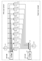
- FIGS. 1 and 2 are diagrams for describing the configuration of the asynchronous FIFO circuit.
- FIG. 3 is a diagram for explaining the operation of the asynchronous FIFO circuit.
- 4 to 5 are diagrams for explaining the effect of the present invention.
- the asynchronous FIFO circuit in the present invention comprises PLL (Phase Locked Loop) 11, DEFINE R generation circuit 12 and FF (Flip Flop) 13 on the write clock side (Write clock domain). ing.
- the asynchronous FIFO circuit also includes a PLL 21, a DEFINER generation circuit 22, and an FF (Flip Flop) 23 on the read clock side (Read clock domain).
- the asynchronous FIFO circuit is provided with a FIFO (First In First Out) 3 for performing data transfer, and the FIFO 3 belongs to both the write clock side and the read clock side.
- the PLL 11 write clock generation unit on the write clock side multiplies the clock CLKA from the input clock CLKA by n to generate a write clock (Write Clock) used in the writing process.
- the PLL 21 read clock generation unit on the read clock side multiplies the clock CLKA by m from the same clock CLKA as the clock input to the PLL 11 on the write clock side, and uses the read clock (Read Clock) is generated.
- the frequency of CLKA 100 MHz
- the write clock 1 GHz
- the read clock 1 GHz
- the write clock read clock.
- the distribution delay from CLKA to PLL 11 shown in FIG. a and the distributed delay b from CLKA to PLL 21 are designed with the same delay.
- the difference between the write timing from the FF 13 to the FIFO 3 and the read timing from the FIFO 3 to the FF 23 is combined with a delay that does not exceed the cycle value of the PLL 11 or PLL 21.
- the timing of writing to the FIFO 3 can be obtained by considering the delay difference between each of the PLLs 11 and 21 to each of the FFs 13 and 23
- the difference in read timing from the FIFO 3 can be made within the cycle of the PLL 11 and the PLL 21. By this, it is not necessary to extend the timing generation of the read processing described later to a value exceeding the cycle value of PLL 11 or PLL 21, and a read pointer that can guarantee delay difference
- the write clock side DEFINE R generation circuit 12 (write control signal generation unit) generates a write DEFINE R signal (write control signal) which is a pulse signal synchronized with the write clock generated by the PLL 11.
- the write DEFINER signal is used to control the write timing of data from the FF 13 by the FIFO 3 as described later.
- the write DEFINER signal synchronized with this write clock is a pulse signal of CLKA cycle.
- the write clock is set to 1 GHz and the write DEFINER signal is set to 100 MHz.
- the DEFINER generation circuit 22 (read control signal generation unit) on the read clock side generates a read DEFINER signal (read control signal) which is a pulse signal synchronized with the read clock generated by the PLL 21.
- the read DEFINER signal is used to control the timing of reading data from the FIFO 3 to the FF 23 as described later.
- the read DEFINER signal synchronized with this read clock is a pulse signal of the CLKA cycle.
- the read clock is set to 1 GHz
- the lead DEFINER signal is set to 100 MHz.
- the same clock CLKA is used as input clocks to the PLLs 11 and 21 different on the write side and the read side, and further, in synchronization with each PLL 11 and 21, a write DEFINER signal is used.
- the lead DEFINER signal is generated. For this reason, as will be described later, the write processing cycle and the read processing cycle operate in a predetermined cycle.
- the FIFO 3 has a write pointer generation circuit 31 on the write clock side and a read pointer generation circuit 32 and a selector 321 on the read clock side.
- the write-to-read transfer part requires a plurality of buffers (data holding units), and the number of buffers is determined by the write clock frequency and the frequency of the write DEFINER signal.
- the write pointer generation circuit 31 starts a series of write processing, and generates a write pointer specifying the buffers 311 to 3110 that write data from the FF 13 to the FIFO 3. Then, the write pointer generation circuit 31 that has started the series of write processing generates a value incremented by one every write clock, that is, each cycle, and uses it as a write pointer. In addition, the write pointer generation circuit 31 starts a series of write processing each time there is an input of a write DEFINER signal, and generates a write pointer having the same value every time the start is performed.
- the write pointer “2” when the write DEFINER signal is input, the write pointer “2” is set, and the write pointer is generated as “3, 4, 5. Next, when the light DEFINER signal is input, "2" is set to the light pointer again.
- the FIFO 3 writes data from the FF 13 to the buffers 311 to 3110 specified by the write pointer generated as described above, for each cycle of the write clock.
- the read pointer generation circuit 32 activates a series of read processing, and generates a read pointer that specifies the buffers 311 to 3110 that read data from the FIFO 3 to the FF 23. Then, the read pointer generation circuit 32 that has started the series of read processing generates a value incremented by one for each read clock, that is, each cycle, and uses it as a read pointer. Also, the read pointer generation circuit 32 starts a series of read processing each time there is an input of a read DEFINER signal, and generates a read pointer of the same value every time the start is performed.
- the read pointer “9” when the read DEFINER signal is input, the read pointer “9” is set, and the read pointer is generated as “10, 1, 2,. Next, when there is an input of the read DEFINER signal, "9" is set to the read pointer again.
- the FIFO 3 selects the buffers 311 to 3110 specified by the read pointer generated as described above by the selector 321 for each cycle of the read clock, and reads data to the FF 23.
- the write pointer generation circuit 31 and the read pointer generation circuit 32 described above write a series of writes at the same timing. It will start processing and a series of reading processing.
- the write pointer generation circuit 31 and the read pointer generation circuit 32 respectively generate different write pointers and read pointers. For example, in the present embodiment, a read pointer three cycles after the write pointer is generated at startup. As a result, the relationship between the read pointer and the write pointer is always ensured, and the read pointer after three cycles is always generated for the write pointer, so that the read process does not overtake the write process.
- the write DEFINER signal indicating the write timing is set at timing 2
- the read DEFINER signal indicating the read timing is also set at timing 2. That is, a series of writing processes and a series of reading processes are activated at the same timing.
- the write pointer generation circuit 31 generates a value incremented for each cycle of the write clock, using the write DEFINER signal as the activation timing, and uses it as the write pointer. At this time, the same pointer value is generated at every activation timing of the write DEFINER signal ("2" in the present embodiment).
- the FIFO 3 writes the data of the FF 13 in the buffer indicated by the write pointer value if the data exists in the FF 13 and writes the indefinite value in the buffer indicated by the write pointer value if the data does not exist.
- the read pointer generation circuit 32 generates a value obtained by incrementing the read DEFINER signal by 1 each cycle as a read processing start timing, and uses the generated value as a read pointer. At this time, the same pointer value is generated at each activation timing of the read DEFINER signal.
- the read pointer “9” is set at each activation since this specification is to read out three cycles after the write timing. That is, the pointer value of the write pointer appears as the pointer value of the read pointer after three cycles.
- the data in the buffers 311 to 3110 is read out in the FF 23 according to the pointer value of the read pointer, and if data does not exist, the undefined value is read out according to the pointer value of the read pointer Be
- processing is performed according to the pointer value in both the write processing and the read processing. Therefore, by matching the pointer values of the write processing and the read processing at a certain timing, the relationship between the read pointer and the write pointer is always ensured, and the read pointer is generated for a write pointer after a certain cycle. There is no need to overtake the write process, and it is possible to change over without performing pointer comparison.
- FIGS. 4 and 5 a comparison of an asynchronous FIFO circuit different from the present invention and the asynchronous FIFO circuit of the present invention is shown.
- the FIFO pointer value is stored as the binary pointer 411, and at time 3, the binary pointer value is gray-coded and stored as the gray pointer 412. Then, in order to stabilize the data, it is stored in the FF 413 at timing 4 as a synchronization FF and in the FF 414 at timing 5. Since the number of FF stages conforms to the circuit rules, two stages are used in this example. After switching to the read side CLK, it is judged by the empty judgment circuit 415 whether or not the FIFO is empty. If it is judged that the FIFO is not empty, the read is performed. Thus, in an asynchronous FIFO circuit different from the present invention, six cycles are required.
- the processing of the present invention is configured to perform write and read regardless of the presence or absence of a request, data control can be simplified. Therefore, it is suitable for processing streaming data to process continuous data.
- the same CLK (CLKA) is used for different PLL inputs.
- the write clock used in the write process is a clock multiplied by n of CLKA
- the clock edge of the write clock is the same as that of CLKA. Therefore, a circuit that generates a pulse signal of CLKA cycles in synchronization with this write clock (
- the circuit configuration uses a DEFINER (generation circuit).
- the read clock used in the read process is a clock multiplied by m of CLKA
- the clock edge of the read clock is the same as that of CLKA. Therefore, a read that generates a pulse signal of CLKA cycles in synchronization with this read clock
- the circuit configuration uses a DEFINER circuit.
- n write data and m read data exist in the CLKA cycle. Therefore, by adjusting m read data not to read n or more write data at the time of design, it is possible to change over in a fixed time from changing over by passing a write pointer and a read pointer, a circuit that can reduce latency. Can be realized.
- the CLKA frequency is 100 MHz
- the write clock is 1 GHz
- the read clock is 1 GHz
- the write FIFO can be prevented from overflowing by providing a cycle in which the write process is not performed.
- the configuration of the above (2) since the data amount of the read process is larger than the data amount of the write process, it is possible to prevent the reading of the data which is not written by providing a cycle in which the read process is not performed. It is.
- FIG. 6 is a block diagram showing the configuration of the asynchronous FIFO circuit in the present embodiment.
- the outline of the configuration of the asynchronous FIFO described in the first embodiment is shown.
- the asynchronous FIFO circuit 100 in this embodiment is: A write clock generation unit 110 that generates a write clock to be used in a write process from the input clock; A read clock generation unit 120 that generates a read clock to be used in a read process from the input clock; A write control signal generation unit 130 that generates a write control signal for controlling data write timing in synchronization with the write clock; A read control signal generation unit 140 that generates a read control signal for controlling data read timing in synchronization with the read clock; A plurality of data holding units 151 are provided, and data is written to any one of the data holding units for each write clock based on the write control signal, and any one for each read clock based on the read control signal. A data read / write unit 150 which reads data from the data holding unit; Is equipped.
- the write clock and the read clock are generated from the same clock, and further, in synchronization with these, the write control signal for controlling the write timing and the read control signal for controlling the read timing are generated. Therefore, since the write cycle and the read cycle operate in a predetermined cycle, it is not necessary to transfer or check data from the write pointer to the read pointer. As a result, the control is not complicated and the latency from write to read can be reduced.
- a write clock generation unit that generates a write clock to be used in a write process from the input clock;
- a read clock generation unit that generates a read clock to be used in read processing from the input clock;
- a write control signal generator for generating a write control signal for controlling data write timing in synchronization with the write clock;
- a read control signal generation unit that generates a read control signal for controlling data read timing in synchronization with the read clock;
- a plurality of data holding units are provided, and data is written to any one of the data holding units for each write clock based on the write control signal, and any one of the data for each read clock based on the read control signal.
- a data read / write unit that reads data from the data holding unit; Equipped with Asynchronous FIFO circuit.
- the asynchronous FIFO circuit according to appendix 3, wherein The data read / write unit generates a write pointer specifying the data holding unit to be written for each write clock, and generates a write pointer generation unit that generates the same write pointer each time the series of write processing is activated. And a read pointer generation unit for generating a read pointer for specifying the data holding unit to be read out for each read clock, and generating the same read pointer for each start of the series of read processes. , Furthermore, the data read / write unit writes data to the data holding unit indicated by the write pointer generated for each write clock, and the data is output from the data holding unit indicated by the read pointer generated for each read clock. read out, Asynchronous FIFO circuit.
- (Appendix 7) Write-side PLL (Phase Locked Loop) that generates a write clock to be used in write processing from the input clock; A read side PLL that generates a read clock used in a read process from the input clock; A write control signal generation circuit that generates a write control signal for controlling data write timing in synchronization with the write clock; A read control signal generation circuit that generates a read control signal for controlling data read timing in synchronization with the read clock; A plurality of buffers are provided, and data is written to any one of the buffers for each write clock based on the write control signal, and data is output from any one of the buffers for each read clock based on the read control signal.
- FIFO to read out Equipped with Asynchronous FIFO circuit.
- Appendix 7.2 The asynchronous FIFO circuit according to appendix 7.1, wherein The FIFO activates the series of write processes and the series of read processes at the same timing based on the write control signal and the read control signal.
- the asynchronous FIFO circuit according to appendix 7.2, wherein The FIFO generates a write pointer that specifies the buffer to be written for each write clock, and a write pointer generation circuit that generates the same write pointer for each start of the series of write processing, and the read And generating a read pointer for specifying the buffer to be read at each clock, and generating a read pointer generation circuit for generating the same read pointer at each start of the series of read processing, Furthermore, the FIFO writes data to the buffer indicated by the write pointer generated for each write clock, and reads data from the buffer indicated by the read pointer generated for each read clock. Asynchronous FIFO circuit.
- appendix 7.4 The asynchronous FIFO circuit according to appendix 7.3, wherein The write pointer generation circuit and the read pointer generation circuit are different in that the write pointer generated at each start of the series of write processing and the read pointer generated at each start of the series of read processing are different. Generating the write pointer and the read pointer respectively to specify a buffer; Asynchronous FIFO circuit.
- An asynchronous FIFO circuit having a plurality of data holding units is While generating a write clock to be used in a writing process from the input clock, and generating a read clock to be used in a reading process from the input clock, A write control signal for controlling data write timing is generated in synchronization with the write clock, and a read control signal for controlling data read timing is generated in synchronization with the read clock, Data is written to any one of the data holding units for each write clock based on the write control signal, and data is read from any one of the data holding units for each read clock based on the read control signal. How to read and write data.
- Appendix 9 It is the data read / write method according to appendix 8. A series of write processes for a plurality of the data holding units are activated based on the write control signal, and a series of read processes for the plurality of data holding units are activated based on the read control signal. How to read and write data.
- Appendix 10.1 It is the data read / write method according to appendix 10.
- a write pointer specifying the data holding unit to be written is generated for each write clock, and the same write pointer is generated for each start of the series of write processing, and a read target is generated for each read clock.
- a read pointer specifying the data holding unit is generated, and the same read pointer is generated each time the series of read processing is started. Writing data in the data holding unit indicated by the write pointer generated for each write clock, and reading data from the data holding unit indicated by the read pointer generated for each read clock; How to read and write data.
Landscapes
- Engineering & Computer Science (AREA)
- Theoretical Computer Science (AREA)
- Physics & Mathematics (AREA)
- General Engineering & Computer Science (AREA)
- General Physics & Mathematics (AREA)
- Synchronisation In Digital Transmission Systems (AREA)
- Information Transfer Systems (AREA)
Abstract
本発明の非同期FIFO回路は、同一の入力クロックからライトクロックとリードクロックとを生成すると共に、ライト制御信号をライトクロックに同期して生成し、リード制御信号をリードクロックに同期して生成する。そして、複数のデータ保持部を有し、ライト制御信号に基づいてライトクロック毎にいずれかのデータ保持部にデータを書き込むと共に、リード制御信号に基づいてリードクロック毎にいずれかのデータ保持部からデータを読み出すデータ読み書き部を備える。
Description
本発明は、非同期FIFO(First In First Out)回路にかかり、特に、Full/Empty判定回路を必要としない非同期FIFO回路に関する。
メモリアクセス等の連続したデータを処理する場合、特許文献1に記載のように、Full/Emptyを判定する回路を設けている場合がある。
上述したFull/Emptyを判定する回路を設けている非同期FIFO回路では、データがFullの場合、データ待ち合わせが発生し、乗換回路の入力部分にバッファが必要になり、制御回路が複雑になる。また、データ幅が広い場合には、物理制約からbit間の乗り換えタイミングが異なるケースも発生し、より制御が難しくなり、データ間の全データが揃うまでの時間も必要になる。
そして、非同期FIFOを使用した乗り換えは、リードポインタがライトポインタを追い越さないチェックを行うために、ライトポインタからリードポインタへのデータの引き渡しを行っていることがある。このような場合、書き込みから読み出しまでのレイテンシが大きくなる、という問題が生じる。
このため、本発明の目的は、上述した課題である、制御が複雑であることと、書き込みから読み出しまでのレイテンシが大きくなる、という問題を解決することができる非同期FIFO回路を提供することにある。
本発明の一形態である非同期FIFO回路は、
入力されたクロックから書き込み処理で用いるライトクロックを生成するライトクロック生成部と、
前記入力されたクロックから読み出し処理で用いるリードクロックを生成するリードクロック生成部と、
データの書き込みタイミングを制御するライト制御信号を前記ライトクロックに同期して生成するライト制御信号生成部と、
データの読み出しタイミングを制御するリード制御信号を前記リードクロックに同期して生成するリード制御信号生成部と、
複数のデータ保持部を有し、前記ライト制御信号に基づいて前記ライトクロック毎にいずれかの前記データ保持部にデータを書き込むと共に、前記リード制御信号に基づいて前記リードクロック毎にいずれかの前記データ保持部からデータを読み出すデータ読み書き部と、
を備えた、
という構成をとる。
入力されたクロックから書き込み処理で用いるライトクロックを生成するライトクロック生成部と、
前記入力されたクロックから読み出し処理で用いるリードクロックを生成するリードクロック生成部と、
データの書き込みタイミングを制御するライト制御信号を前記ライトクロックに同期して生成するライト制御信号生成部と、
データの読み出しタイミングを制御するリード制御信号を前記リードクロックに同期して生成するリード制御信号生成部と、
複数のデータ保持部を有し、前記ライト制御信号に基づいて前記ライトクロック毎にいずれかの前記データ保持部にデータを書き込むと共に、前記リード制御信号に基づいて前記リードクロック毎にいずれかの前記データ保持部からデータを読み出すデータ読み書き部と、
を備えた、
という構成をとる。
また、本発明の一形態である非同期FIFO回路は、
入力されたクロックから書き込み処理で用いるライトクロックを生成するライト側PLL(Phase Locked Loop)と、
前記入力されたクロックから読み出し処理で用いるリードクロックを生成するリード側PLLと、
データの書き込みタイミングを制御するライト制御信号を前記ライトクロックに同期して生成するライト制御信号生成回路と、
データの読み出しタイミングを制御するリード制御信号を前記リードクロックに同期して生成するリード制御信号生成回路と、
複数のバッファを有し、前記ライト制御信号に基づいて前記ライトクロック毎にいずれかの前記バッファにデータを書き込むと共に、前記リード制御信号に基づいて前記リードクロック毎にいずれかの前記バッファからデータを読み出すFIFOと、
を備えた、
という構成をとる。
入力されたクロックから書き込み処理で用いるライトクロックを生成するライト側PLL(Phase Locked Loop)と、
前記入力されたクロックから読み出し処理で用いるリードクロックを生成するリード側PLLと、
データの書き込みタイミングを制御するライト制御信号を前記ライトクロックに同期して生成するライト制御信号生成回路と、
データの読み出しタイミングを制御するリード制御信号を前記リードクロックに同期して生成するリード制御信号生成回路と、
複数のバッファを有し、前記ライト制御信号に基づいて前記ライトクロック毎にいずれかの前記バッファにデータを書き込むと共に、前記リード制御信号に基づいて前記リードクロック毎にいずれかの前記バッファからデータを読み出すFIFOと、
を備えた、
という構成をとる。
また、本発明の一形態であるデータ読み書き方法は、
複数のデータ保持部を有する非同期FIFO回路が、
入力されたクロックから書き込み処理で用いるライトクロックを生成すると共に、前記入力されたクロックから読み出し処理で用いるリードクロックを生成し、
データの書き込みタイミングを制御するライト制御信号を前記ライトクロックに同期して生成すると共に、データの読み出しタイミングを制御するリード制御信号を前記リードクロックに同期して生成し、
前記ライト制御信号に基づいて前記ライトクロック毎にいずれかの前記データ保持部にデータを書き込むと共に、前記リード制御信号に基づいて前記リードクロック毎にいずれかの前記データ保持部からデータを読み出す、
という構成をとる。
複数のデータ保持部を有する非同期FIFO回路が、
入力されたクロックから書き込み処理で用いるライトクロックを生成すると共に、前記入力されたクロックから読み出し処理で用いるリードクロックを生成し、
データの書き込みタイミングを制御するライト制御信号を前記ライトクロックに同期して生成すると共に、データの読み出しタイミングを制御するリード制御信号を前記リードクロックに同期して生成し、
前記ライト制御信号に基づいて前記ライトクロック毎にいずれかの前記データ保持部にデータを書き込むと共に、前記リード制御信号に基づいて前記リードクロック毎にいずれかの前記データ保持部からデータを読み出す、
という構成をとる。
本発明は、以上のように構成されることにより、制御が複雑ではなく、書き込みから読み出しまでのレイテンシを減少させることができる非同期FIFO回路を提供することができる。
<実施形態1>
本発明の第1の実施形態を、図1乃至図5を参照して説明する。図1乃至2は、非同期FIFO回路の構成を説明するための図である。図3は、非同期FIFO回路の動作を説明するための図である。図4乃至図5は、本発明の効果を説明するための図である。
本発明の第1の実施形態を、図1乃至図5を参照して説明する。図1乃至2は、非同期FIFO回路の構成を説明するための図である。図3は、非同期FIFO回路の動作を説明するための図である。図4乃至図5は、本発明の効果を説明するための図である。
[構成]
図1に示すように、本発明における非同期FIFO回路は、ライトクロック側(Write clock domain)に、PLL(Phase Locked Loop)11と、DEFINER生成回路12と、FF(Flip Flop)13と、を備えている。また、非同期FIFO回路は、リードクロック側(Read clock domain)にも同様に、PLL21と、DEFINER生成回路22と、FF(Flip Flop)23と、を備えている。さらに、非同期FIFO回路は、データの乗り換えを行うFIFO(First In First Out)3を備えており、当該FIFO3はライトクロック側及びリードクロック側の両側に属している。
図1に示すように、本発明における非同期FIFO回路は、ライトクロック側(Write clock domain)に、PLL(Phase Locked Loop)11と、DEFINER生成回路12と、FF(Flip Flop)13と、を備えている。また、非同期FIFO回路は、リードクロック側(Read clock domain)にも同様に、PLL21と、DEFINER生成回路22と、FF(Flip Flop)23と、を備えている。さらに、非同期FIFO回路は、データの乗り換えを行うFIFO(First In First Out)3を備えており、当該FIFO3はライトクロック側及びリードクロック側の両側に属している。
上記ライトクロック側のPLL11(ライトクロック生成部)は、入力されたクロックCLKAから当該クロックCLKAをn逓倍して、書き込み処理で用いるライトクロック(Write Clock)を生成する。また、上記リードクロック側のPLL21(リードクロック生成部)は、上記ライトクロック側のPLL11に入力されるクロックと同一のクロックCLKAから当該クロックCLKAをm逓倍して、読み出し処理で用いるリードクロック(Read Clock)を生成する。本実施形態では、例えば、CLKAの周波数=100MHz、ライトクロック=1GHz、リードクロック=1GHzであり、ライトクロック=リードクロックであることとする。
なお、本実施形態では、後述するように、ライト側のFF13からFIFO3への書き込みタイミングと、リード側のFIFO3からFF23への読み出しタイミングを同期させるために、図1に示すCLKAからPLL11まで分配遅延aと、CLKAからPLL21までに分配遅延bとを、同遅延で設計している。
また、本実施形態では、更にFF13からFIFO3への書き込みタイミングと、FIFO3からFF23への読み出しタイミングの差を、PLL11やPLL21のサイクル値を超えない程度の遅延で合わせこむ。このとき、上記各PLL11,21までの遅延を同遅延としているので、各PLL11,21から各FF13,23までの遅延差|遅延x-遅延y|を考慮する事で、FIFO3への書き込みタイミングとFIFO3からの読み出しタイミングの差を、PLL11やPLL21のサイクル内に収めることができる。これにより、後述するリード処理のタイミング生成を、PLL11やPLL21のサイクル値を超えた値まで拡げる必要はなく、遅延差|遅延x-遅延y|を保証できるリードポインタを設定すればよい。
上記ライトクロック側のDEFINER生成回路12(ライト制御信号生成部)は、上記PLL11で生成されたライトクロックに同期したパルス信号であるライトDEFINER信号(ライト制御信号)を生成する。ライトDEFINER信号は、後述するように、FIFO3によるFF13からデータの書き込みタイミングを制御するために用いられる。
なお、ライトDEFINER信号の元となるライトクロックは、CLKAとクロックエッジが一致しているため、このライトクロックと同期するライトDEFINER信号は、CLKAサイクルのパルス信号となる。例えば、本実施形態では、ライトクロック=1GHz、ライトDEFINER信号=100MHzで設定される。
同様に、上記リードクロック側のDEFINER生成回路22(リード制御信号生成部)は、上記PLL21で生成されたリードクロックに同期したパルス信号であるリードDEFINER信号(リード制御信号)を生成する。リードDEFINER信号は、後述するように、FIFO3からFF23へのデータの読み出しタイミングを制御するために用いられる。
なお、リードDEFINER信号の元となるリードクロックは、CLKAとクロックエッジが一致しているため、このリードクロックと同期するリードDEFINER信号は、CLKAサイクルのパルス信号となる。例えば、本実施形態では、リードクロック=1GHz、リードDEFINER信号=100MHzで設定される。
このように、本実施形態では、ライト側とリード側との異なるPLL11,21への入力クロックに、同一クロックCLKAを使用しており、さらに、各PLL11,21に同期してそれぞれライトDEFINER信号とリードDEFINER信号とを生成している。このため、後述するように、書き込み処理のサイクルと読み出し処理のサイクルとは、ある決まったサイクルで作動することとなる。
上記FIFO3は、図2に示すように、ライトクロック側ではライトポインタ生成回路31を有し、リードクロック側ではリードポインタ生成回路32とセレクタ321を有する。ライトからリードへの乗り換え部分では、複数のバッファ(データ保持部)が必要であり、バッファ数は、ライトクロック周波数とライトDEFINER信号の周波数で決定される。本実施形態では、ライトクロック=1GHz、ライトDEFINER信号=100MHzであるため、図2に示すように、バッファ数は、DEFINERサイクルでライトデータが書き込める最大数が10となり、10段のバッファ311~3110からなる。なお、本実施形態では、リードDEFINER信号=100MHzであることとする。
上記ライトポインタ生成回路31は、ライトDEFINER信号の入力があったときに、一連の書き込み処理を起動して、FF13からFIFO3にデータを書き込むバッファ311~3110を特定するライトポインタを生成する。そして、一連の書き込み処理を起動したライトポインタ生成回路31は、ライトクロック毎つまりサイクル毎に、1インクリメントした値を生成してライトポインタとして使用する。また、ライトポインタ生成回路31は、ライトDEFINER信号の入力がある毎に、一連の書き込み処理を起動して、かかる起動毎に同一の値のライトポインタを生成する。例えば、本実施形態では、ライトDEFINER信号の入力があったときに、ライトポインタ「2」を設定し、ライトクロックのサイクル毎にライトポインタが「3,4,5・・・」と生成され、次にライトDEFINER信号の入力があると再度ライトポインタに「2」が設定される。
そして、FIFO3は、ライトクロックのサイクル毎に、上述したように生成されたライトポインタにて特定されるバッファ311~3110に、FF13からデータを書き込む。
上記リードポインタ生成回路32は、リードDEFINER信号の入力があったときに、一連の読み出し処理を起動して、FIFO3からFF23にデータを読み出すバッファ311~3110を特定するリードポインタを生成する。そして、一連の読み出し処理を起動したリードポインタ生成回路32は、リードクロック毎つまりサイクル毎に、1インクリメントした値を生成してリードポインタとして使用する。また、リードポインタ生成回路32は、リードDEFINER信号の入力がある毎に、一連の読み出し処理を起動して、かかる起動毎に同一の値のリードポインタを生成する。例えば、本実施形態では、リードDEFINER信号の入力があったときに、リードポインタ「9」を設定し、リードクロックのサイクル毎にリードポインタが「10,1,2・・・」と生成され、次にリードDEFINER信号の入力があると再度リードポインタに「9」が設定される。
そして、FIFO3は、リードクロックのサイクル毎に、上述したように生成されたリードポインタにて特定されるバッファ311~3110をセレクタ321で選択し、FF23にデータを読み出す。
なお、本実施形態では、FIFO3は、ライトDEFINER信号とリードDEFINER信号とが同一のタイミングであることから、上述したライトポインタ生成回路31とリードポインタ生成回路32とは、同一のタイミングで一連の書き込み処理と一連の読み出し処理を起動することとなる。そして、この起動時に、ライトポインタ生成回路31とリードポインタ生成回路32とは、相互に異なるライトポインタとリードポインタとをそれぞれ生成している。例えば、本実施形態では、起動時に、ライトポインタに対して、3サイクル後のリードポインタが生成される。これにより、リードポインタとライトポインタの関係が常時保障され、常にライトポインタに対して、3サイクル後のリードポインタを生成するので、リード処理がライト処理を追い越すことがなくなる。
[動作]
次に、図3のタイムチャートを参照して、上述した非同期FIFO回路によるFIFO3にデータを書き込んで読み出すまでの動作を説明する。
次に、図3のタイムチャートを参照して、上述した非同期FIFO回路によるFIFO3にデータを書き込んで読み出すまでの動作を説明する。
まず、CLKAからPLL11とPLL21までの遅延は等遅延なので、書き込みタイミングを示すライトDEFINER信号がタイミング2でセットされると、読み出しタイミングを示すリードDEFINER信号もタイミング2でセットされる。つまり、同一のタイミングで、一連の書き込み処理と一連の読み出し処理が起動される。
上記状況において、まず書き込み処理について説明する。ライトポインタ生成回路31は、ライトDEFINER信号を起動タイミングとして、ライトクロックのサイクル毎にインクリメントした値を生成し、ライトポインタとして使用する。このとき、ライトDEFINER信号の起動タイミング毎に、同じポインタ値を生成する(本実施形態では「2」)。
そして、FIFO3は、FF13にデータが存在すれば、ライトポインタ値で示されるバッファにFF13のデータをライトし、データが存在しなければ、ライトポインタ値で示されるバッファに不定値をライトする。図3に示すように、タイミング1ではFF13にデータ「1」があり、ライトポインタ生成回路31のポインタ値=1であるため、タイミング1でバッファ311へのデータセット指示が出され、タイミング2で、バッファ311にデータが保持される。なお、このバッファ311に次のデータがセットされるのは、ライトポインタ=1になるタイミング11で指示が出された次のタイミング12となる。
同様に、タイミング2のFF13のデータ「2」は、タイミング2でデータセット指示が出るので、タイミング3でバッファ312にデータが保持されていく。この書き込み処理は、FF13にデータがある場合、ライトポインタ生成回路31のポインタ値に従い、実施されていく。
次に、リード処理について説明する。リードポインタ生成回路32は、リードDEFINER信号をリード処理の起動タイミングとして、サイクル毎に1インクリメントした値を生成し、リードポインタとして使用する。このときリードDEFINER信号の起動タイミング毎に、同じポインタ値を生成する。本例では、ライトタイミングの3サイクル後に読み出す仕様なので、起動毎にリードポインタ「9」をセットする。つまり、ライトポインタのポインタ値が3サイクル後に、リードポインタのポインタ値として現れる。バッファ311~3110内にデータが存在する場合、リードポインタのポインタ値に従い、FF23にバッファ311~3110内のデータが読み出され、データが存在しない場合、リードポインタのポインタ値に従い、不定値が読み出される。
本発明の乗り換え回路では、ライト処理・リード処理ともポインタ値に従い処理を行う。そのため、あるタイミングでライト処理とリード処理のポインタ値を一致させることでリードポインタとライトポインタの関係が常時保障され、常にライトポインタに対して、一定サイクル後のリードポインタを生成するため、リード処理がライト処理を追い越す事はなくなり、ポインタ比較を行うことなく乗り換えが可能となる。
ここで、図4及び図5を参照して、本発明とは異なる非同期FIFO回路と本発明の非同期FIFO回路との比較を示す。
図4に示す本発明とは異なる非同期FIFO回路では、書き込みFF4から読み出しFF42までのデータ処理の流れを見ると、まず、書き込みFF4からFIFO41にデータをタイミング2で書き込む。同時にFIFOのポインタ値をバイナリポインタ411として格納し、タイミング3でバイナリポインタ値のグレイコード化を行い、グレイポインター412として格納する。そして、データを安定化させるため同期化FFとしてタイミング4でFF413、タイミング5でFF414に格納する。FF段数は回路規則に従うので、本例では2段としている。リード側CLKに乗り換えた後、FIFOが空かどうかをempty判定回路415で判定し、emptyでないと判定されればリードを行う。このように、本発明とは異なる非同期FIFO回路では、6サイクルが必要である。
一方、本発明においては、ポインタの比較でemptyの判定を行わないため、グレイコード化やFFでの安定化が必要なくなる。そのため、図4に示す符号412~415の回路が不要になる。その結果、本発明では、図5に示すように、タイミング4でリード処理が可能となり、2サイクルの高速化が実現でき、レイテンシを短くすることができる。
更に、本発明の処理は、リクエストの有無に関係なくライト・リードを行う構成になっているためデータ制御が簡素化できる。このため、連続したデータを処理するストリーミングデータの処理を行うのに適している。
以上のように、本発明では、異なるPLLドメイン間のデータ転送において、異なるPLL入力に同一CLK(CLKA)を使用する回路構成としている。そして、ライト処理で使用するライトクロックをCLKAのn逓倍したクロックとした場合、ライトクロックはCLKAとクロックエッジが一致しているため、このライトクロック同期してCLKAサイクルのパルス信号を生成する回路(DEFINER生成回路)を使用する回路構成としている。また、リード処理で使用するリードクロックをCLKAのm逓倍したクロックとした場合、リードクロックはCLKAとクロックエッジが一致しているので、このリードクロックに同期してCLKAサイクルのパルス信号を生成するリードDEFINER回路を使用する回路構成としている。
上記3つの回路を実装し、ライト側のDEFINER回路とリード側のDEFINER回路を使用することで、CLKAサイクル内にn個のライトデータとm個のリードデータが存在する事がわかる。そこで、設計時にm個のリードデータはn個以上のライトデータを読み出さないように調整する事で、ライトポインタとリードポインタの引き渡しによる乗り換えから固定時間での乗り換えが可能となり、レイテンシを短縮できる回路が実現できる。
なお、上記実施形態では、CLKAの周波数=100MHz、ライトクロック=1GHz、リードクロック=1GHzであり、ライトクロック=リードクロックの条件で適用可能な構成を例示したが、本発明の非同期FIFO回路は、以下の条件でも適用可能である。
(1)ライトクロック(高周波)>リードクロック(低周波)
(2)ライトクロック(低周波)<リードクロック(高周波)
(1)ライトクロック(高周波)>リードクロック(低周波)
(2)ライトクロック(低周波)<リードクロック(高周波)
上記(1)の構成では、ライト処理のデータ量がリード処理のデータ量より多いので、ライト処理を行わないサイクルを設けることで、書き込みFIFOがオーバーフローする事を防いで処理が可能である。同様に、上記(2)の構成では、リード処理のデータ量がライト処理のデータ量より多いので、リード処理を行わないサイクルを設けることで、書き込んでいないデータを読み出す事を防いで処理が可能である。
<実施形態2>
次に、本発明の第2の実施形態を、図6を参照して説明する。図6は、本実施形態における非同期FIFO回路の構成を示すブロック図である。なお、本実施形態では、実施形態1で説明した非同期FIFOの構成の概略を示している。
次に、本発明の第2の実施形態を、図6を参照して説明する。図6は、本実施形態における非同期FIFO回路の構成を示すブロック図である。なお、本実施形態では、実施形態1で説明した非同期FIFOの構成の概略を示している。
図6に示すように、本実施形態おける非同期FIFO回路100は、
入力されたクロックから書き込み処理で用いるライトクロックを生成するライトクロック生成部110と、
前記入力されたクロックから読み出し処理で用いるリードクロックを生成するリードクロック生成部120と、
データの書き込みタイミングを制御するライト制御信号を前記ライトクロックに同期して生成するライト制御信号生成部130と、
データの読み出しタイミングを制御するリード制御信号を前記リードクロックに同期して生成するリード制御信号生成部140と、
複数のデータ保持部151を有し、前記ライト制御信号に基づいて前記ライトクロック毎にいずれかの前記データ保持部にデータを書き込むと共に、前記リード制御信号に基づいて前記リードクロック毎にいずれかの前記データ保持部からデータを読み出すデータ読み書き部150と、
を備えている。
入力されたクロックから書き込み処理で用いるライトクロックを生成するライトクロック生成部110と、
前記入力されたクロックから読み出し処理で用いるリードクロックを生成するリードクロック生成部120と、
データの書き込みタイミングを制御するライト制御信号を前記ライトクロックに同期して生成するライト制御信号生成部130と、
データの読み出しタイミングを制御するリード制御信号を前記リードクロックに同期して生成するリード制御信号生成部140と、
複数のデータ保持部151を有し、前記ライト制御信号に基づいて前記ライトクロック毎にいずれかの前記データ保持部にデータを書き込むと共に、前記リード制御信号に基づいて前記リードクロック毎にいずれかの前記データ保持部からデータを読み出すデータ読み書き部150と、
を備えている。
上記発明によると、同一のクロックからライトクロック及びリードクロックを生成し、さらに、これらに同期して、書き込みタイミングを制御するライト制御信号と読み出しタイミングを制御するリード制御信号とを生成している。このため、ライトサイクルとリードサイクルとは、ある決まったサイクルで動作することになるため、ライトポインタからリードポインタへのデータの引き渡しやチェックが不要になる。その結果、制御が複雑ではなく、書き込みから読み出しまでのレイテンシを減少させることができる。
<付記>
上記実施形態の一部又は全部は、以下の付記のようにも記載されうる。以下、本発明における非同期FIFO回路、データ読み書き方法の構成の概略を説明する。但し、本発明は、以下の構成に限定されない。
上記実施形態の一部又は全部は、以下の付記のようにも記載されうる。以下、本発明における非同期FIFO回路、データ読み書き方法の構成の概略を説明する。但し、本発明は、以下の構成に限定されない。
(付記1)
入力されたクロックから書き込み処理で用いるライトクロックを生成するライトクロック生成部と、
前記入力されたクロックから読み出し処理で用いるリードクロックを生成するリードクロック生成部と、
データの書き込みタイミングを制御するライト制御信号を前記ライトクロックに同期して生成するライト制御信号生成部と、
データの読み出しタイミングを制御するリード制御信号を前記リードクロックに同期して生成するリード制御信号生成部と、
複数のデータ保持部を有し、前記ライト制御信号に基づいて前記ライトクロック毎にいずれかの前記データ保持部にデータを書き込むと共に、前記リード制御信号に基づいて前記リードクロック毎にいずれかの前記データ保持部からデータを読み出すデータ読み書き部と、
を備えた、
非同期FIFO回路。
入力されたクロックから書き込み処理で用いるライトクロックを生成するライトクロック生成部と、
前記入力されたクロックから読み出し処理で用いるリードクロックを生成するリードクロック生成部と、
データの書き込みタイミングを制御するライト制御信号を前記ライトクロックに同期して生成するライト制御信号生成部と、
データの読み出しタイミングを制御するリード制御信号を前記リードクロックに同期して生成するリード制御信号生成部と、
複数のデータ保持部を有し、前記ライト制御信号に基づいて前記ライトクロック毎にいずれかの前記データ保持部にデータを書き込むと共に、前記リード制御信号に基づいて前記リードクロック毎にいずれかの前記データ保持部からデータを読み出すデータ読み書き部と、
を備えた、
非同期FIFO回路。
(付記2)
付記1に記載の非同期FIFO回路であって、
前記データ読み書き部は、前記ライト制御信号に基づいて複数の前記データ保持部に対する一連の書き込み処理を起動すると共に、前記リード制御信号に基づいて複数の前記データ保持部に対する一連の読み出し処理を起動する、
非同期FIFO回路。
付記1に記載の非同期FIFO回路であって、
前記データ読み書き部は、前記ライト制御信号に基づいて複数の前記データ保持部に対する一連の書き込み処理を起動すると共に、前記リード制御信号に基づいて複数の前記データ保持部に対する一連の読み出し処理を起動する、
非同期FIFO回路。
(付記3)
付記2に記載の非同期FIFO回路であって、
前記データ読み書き部は、前記ライト制御信号と前記リード制御信号とに基づいて、前記一連の書き込み処理と前記一連の読み出し処理とを同一のタイミングで起動する、
非同期FIFO回路。
付記2に記載の非同期FIFO回路であって、
前記データ読み書き部は、前記ライト制御信号と前記リード制御信号とに基づいて、前記一連の書き込み処理と前記一連の読み出し処理とを同一のタイミングで起動する、
非同期FIFO回路。
(付記4)
付記3に記載の非同期FIFO回路であって、
前記データ読み書き部は、前記ライトクロック毎に書き込み対象となる前記データ保持部を特定するライトポインタを生成すると共に、前記一連の書き込み処理の起動毎に同一の前記ライトポインタを生成するライトポインタ生成部と、前記リードクロック毎に読み出し対象となる前記データ保持部を特定するリードポインタを生成すると共に、前記一連の読み出し処理の起動毎に同一の前記リードポインタを生成するリードポインタ生成部と、を備え、
さらに、前記データ読み書き部は、前記ライトクロック毎に生成された前記ライトポインタが示す前記データ保持部にデータを書き込み、前記リードクロック毎に生成された前記リードポインタが示す前記データ保持部からデータを読み出す、
非同期FIFO回路。
付記3に記載の非同期FIFO回路であって、
前記データ読み書き部は、前記ライトクロック毎に書き込み対象となる前記データ保持部を特定するライトポインタを生成すると共に、前記一連の書き込み処理の起動毎に同一の前記ライトポインタを生成するライトポインタ生成部と、前記リードクロック毎に読み出し対象となる前記データ保持部を特定するリードポインタを生成すると共に、前記一連の読み出し処理の起動毎に同一の前記リードポインタを生成するリードポインタ生成部と、を備え、
さらに、前記データ読み書き部は、前記ライトクロック毎に生成された前記ライトポインタが示す前記データ保持部にデータを書き込み、前記リードクロック毎に生成された前記リードポインタが示す前記データ保持部からデータを読み出す、
非同期FIFO回路。
(付記5)
付記4に記載の非同期FIFO回路であって、
前記ライトポインタ生成部と前記リードポインタ生成部とは、前記一連の書き込み処理の起動毎に生成する前記ライトポインタと、前記一連の読み出し処理の起動毎に生成する前記リードポインタとが、それぞれ異なる前記データ保持部を特定するよう前記ライトポインタと前記リードポインタとをそれぞれ生成する、
非同期FIFO回路。
付記4に記載の非同期FIFO回路であって、
前記ライトポインタ生成部と前記リードポインタ生成部とは、前記一連の書き込み処理の起動毎に生成する前記ライトポインタと、前記一連の読み出し処理の起動毎に生成する前記リードポインタとが、それぞれ異なる前記データ保持部を特定するよう前記ライトポインタと前記リードポインタとをそれぞれ生成する、
非同期FIFO回路。
(付記6)
付記1乃至5のいずれかに記載の非同期FIFO回路であって、
前記入力されたクロックのクロック源から、前記ライトクロック生成部と前記リードクロック生成部までのそれぞれの遅延が同一となる設定されている、
非同期FIFO回路。
付記1乃至5のいずれかに記載の非同期FIFO回路であって、
前記入力されたクロックのクロック源から、前記ライトクロック生成部と前記リードクロック生成部までのそれぞれの遅延が同一となる設定されている、
非同期FIFO回路。
(付記7)
入力されたクロックから書き込み処理で用いるライトクロックを生成するライト側PLL(Phase Locked Loop)と、
前記入力されたクロックから読み出し処理で用いるリードクロックを生成するリード側PLLと、
データの書き込みタイミングを制御するライト制御信号を前記ライトクロックに同期して生成するライト制御信号生成回路と、
データの読み出しタイミングを制御するリード制御信号を前記リードクロックに同期して生成するリード制御信号生成回路と、
複数のバッファを有し、前記ライト制御信号に基づいて前記ライトクロック毎にいずれかの前記バッファにデータを書き込むと共に、前記リード制御信号に基づいて前記リードクロック毎にいずれかの前記バッファからデータを読み出すFIFOと、
を備えた、
非同期FIFO回路。
入力されたクロックから書き込み処理で用いるライトクロックを生成するライト側PLL(Phase Locked Loop)と、
前記入力されたクロックから読み出し処理で用いるリードクロックを生成するリード側PLLと、
データの書き込みタイミングを制御するライト制御信号を前記ライトクロックに同期して生成するライト制御信号生成回路と、
データの読み出しタイミングを制御するリード制御信号を前記リードクロックに同期して生成するリード制御信号生成回路と、
複数のバッファを有し、前記ライト制御信号に基づいて前記ライトクロック毎にいずれかの前記バッファにデータを書き込むと共に、前記リード制御信号に基づいて前記リードクロック毎にいずれかの前記バッファからデータを読み出すFIFOと、
を備えた、
非同期FIFO回路。
(付記7.1)
付記7に記載の非同期FIFO回路であって、
前記FIFOは、前記ライト制御信号に基づいて複数の前記バッファに対する一連の書き込み処理を起動すると共に、前記リード制御信号に基づいて複数の前記バッファに対する一連の読み出し処理を起動する、
非同期FIFO回路。
付記7に記載の非同期FIFO回路であって、
前記FIFOは、前記ライト制御信号に基づいて複数の前記バッファに対する一連の書き込み処理を起動すると共に、前記リード制御信号に基づいて複数の前記バッファに対する一連の読み出し処理を起動する、
非同期FIFO回路。
(付記7.2)
付記7.1に記載の非同期FIFO回路であって、
前記FIFOは、前記ライト制御信号と前記リード制御信号とに基づいて、前記一連の書き込み処理と前記一連の読み出し処理とを同一のタイミングで起動する、
非同期FIFO回路。
付記7.1に記載の非同期FIFO回路であって、
前記FIFOは、前記ライト制御信号と前記リード制御信号とに基づいて、前記一連の書き込み処理と前記一連の読み出し処理とを同一のタイミングで起動する、
非同期FIFO回路。
(付記7.3)
付記7.2に記載の非同期FIFO回路であって、
前記FIFOは、前記ライトクロック毎に書き込み対象となる前記バッファを特定するライトポインタを生成すると共に、前記一連の書き込み処理の起動毎に同一の前記ライトポインタを生成するライトポインタ生成回路と、前記リードクロック毎に読み出し対象となる前記バッファを特定するリードポインタを生成すると共に、前記一連の読み出し処理の起動毎に同一の前記リードポインタを生成するリードポインタ生成回路と、を備え、
さらに、前記FIFOは、前記ライトクロック毎に生成された前記ライトポインタが示す前記バッファにデータを書き込み、前記リードクロック毎に生成された前記リードポインタが示す前記バッファからデータを読み出す、
非同期FIFO回路。
付記7.2に記載の非同期FIFO回路であって、
前記FIFOは、前記ライトクロック毎に書き込み対象となる前記バッファを特定するライトポインタを生成すると共に、前記一連の書き込み処理の起動毎に同一の前記ライトポインタを生成するライトポインタ生成回路と、前記リードクロック毎に読み出し対象となる前記バッファを特定するリードポインタを生成すると共に、前記一連の読み出し処理の起動毎に同一の前記リードポインタを生成するリードポインタ生成回路と、を備え、
さらに、前記FIFOは、前記ライトクロック毎に生成された前記ライトポインタが示す前記バッファにデータを書き込み、前記リードクロック毎に生成された前記リードポインタが示す前記バッファからデータを読み出す、
非同期FIFO回路。
(付記7.4)
付記7.3に記載の非同期FIFO回路であって、
前記ライトポインタ生成回路と前記リードポインタ生成回路とは、前記一連の書き込み処理の起動毎に生成する前記ライトポインタと、前記一連の読み出し処理の起動毎に生成する前記リードポインタとが、それぞれ異なる前記バッファを特定するよう前記ライトポインタと前記リードポインタとをそれぞれ生成する、
非同期FIFO回路。
付記7.3に記載の非同期FIFO回路であって、
前記ライトポインタ生成回路と前記リードポインタ生成回路とは、前記一連の書き込み処理の起動毎に生成する前記ライトポインタと、前記一連の読み出し処理の起動毎に生成する前記リードポインタとが、それぞれ異なる前記バッファを特定するよう前記ライトポインタと前記リードポインタとをそれぞれ生成する、
非同期FIFO回路。
(付記7.5)
付記7乃至7.4のいずれかに記載の非同期FIFO回路であって、
前記入力されたクロックのクロック源から、前記ライト側PLLと前記リード側PLLまでのそれぞれの遅延が同一となる設定されている、
非同期FIFO回路。
付記7乃至7.4のいずれかに記載の非同期FIFO回路であって、
前記入力されたクロックのクロック源から、前記ライト側PLLと前記リード側PLLまでのそれぞれの遅延が同一となる設定されている、
非同期FIFO回路。
(付記8)
複数のデータ保持部を有する非同期FIFO回路が、
入力されたクロックから書き込み処理で用いるライトクロックを生成すると共に、前記入力されたクロックから読み出し処理で用いるリードクロックを生成し、
データの書き込みタイミングを制御するライト制御信号を前記ライトクロックに同期して生成すると共に、データの読み出しタイミングを制御するリード制御信号を前記リードクロックに同期して生成し、
前記ライト制御信号に基づいて前記ライトクロック毎にいずれかの前記データ保持部にデータを書き込むと共に、前記リード制御信号に基づいて前記リードクロック毎にいずれかの前記データ保持部からデータを読み出す、
データ読み書き方法。
複数のデータ保持部を有する非同期FIFO回路が、
入力されたクロックから書き込み処理で用いるライトクロックを生成すると共に、前記入力されたクロックから読み出し処理で用いるリードクロックを生成し、
データの書き込みタイミングを制御するライト制御信号を前記ライトクロックに同期して生成すると共に、データの読み出しタイミングを制御するリード制御信号を前記リードクロックに同期して生成し、
前記ライト制御信号に基づいて前記ライトクロック毎にいずれかの前記データ保持部にデータを書き込むと共に、前記リード制御信号に基づいて前記リードクロック毎にいずれかの前記データ保持部からデータを読み出す、
データ読み書き方法。
(付記9)
付記8に記載のデータ読み書き方法であって、
前記ライト制御信号に基づいて複数の前記データ保持部に対する一連の書き込み処理を起動すると共に、前記リード制御信号に基づいて複数の前記データ保持部に対する一連の読み出し処理を起動する、
データ読み書き方法。
付記8に記載のデータ読み書き方法であって、
前記ライト制御信号に基づいて複数の前記データ保持部に対する一連の書き込み処理を起動すると共に、前記リード制御信号に基づいて複数の前記データ保持部に対する一連の読み出し処理を起動する、
データ読み書き方法。
(付記10)
付記9に記載のデータ読み書き方法であって、
前記ライト制御信号と前記リード制御信号とに基づいて、前記一連の書き込み処理と前記一連の読み出し処理とを同一のタイミングで起動する、
データ読み書き方法。
付記9に記載のデータ読み書き方法であって、
前記ライト制御信号と前記リード制御信号とに基づいて、前記一連の書き込み処理と前記一連の読み出し処理とを同一のタイミングで起動する、
データ読み書き方法。
(付記10.1)
付記10に記載のデータ読み書き方法であって、
前記ライトクロック毎に書き込み対象となる前記データ保持部を特定するライトポインタを生成すると共に、前記一連の書き込み処理の起動毎に同一の前記ライトポインタを生成し、前記リードクロック毎に読み出し対象となる前記データ保持部を特定するリードポインタを生成すると共に、前記一連の読み出し処理の起動毎に同一の前記リードポインタを生成し、
前記ライトクロック毎に生成された前記ライトポインタが示す前記データ保持部にデータを書き込み、前記リードクロック毎に生成された前記リードポインタが示す前記データ保持部からデータを読み出す、
データ読み書き方法。
付記10に記載のデータ読み書き方法であって、
前記ライトクロック毎に書き込み対象となる前記データ保持部を特定するライトポインタを生成すると共に、前記一連の書き込み処理の起動毎に同一の前記ライトポインタを生成し、前記リードクロック毎に読み出し対象となる前記データ保持部を特定するリードポインタを生成すると共に、前記一連の読み出し処理の起動毎に同一の前記リードポインタを生成し、
前記ライトクロック毎に生成された前記ライトポインタが示す前記データ保持部にデータを書き込み、前記リードクロック毎に生成された前記リードポインタが示す前記データ保持部からデータを読み出す、
データ読み書き方法。
(付記10.2)
付記10.1に記載のデータ読み書き方法であって、
前記一連の書き込み処理の起動毎に生成する前記ライトポインタと、前記一連の読み出し処理の起動毎に生成する前記リードポインタとが、それぞれ異なる前記データ保持部を特定するよう前記ライトポインタと前記リードポインタとをそれぞれ生成する、
データ読み書き方法。
付記10.1に記載のデータ読み書き方法であって、
前記一連の書き込み処理の起動毎に生成する前記ライトポインタと、前記一連の読み出し処理の起動毎に生成する前記リードポインタとが、それぞれ異なる前記データ保持部を特定するよう前記ライトポインタと前記リードポインタとをそれぞれ生成する、
データ読み書き方法。
以上、上記実施形態等を参照して本願発明を説明したが、本願発明は、上述した実施形態に限定されるものではない。本願発明の構成や詳細には、本願発明の範囲内で当業者が理解しうる様々な変更をすることができる。
なお、本発明は、日本国にて2017年10月19日に特許出願された特願2017-202859の特許出願に基づく優先権主張の利益を享受するものであり、当該特許出願に記載された内容は、全て本明細書に含まれるものとする。
11,21 PLL
12,22 DEFINER生成回路
13,23 FF
3 FIFO
31 ライトポインタ生成回路
32 リードポインタ生成回路
311~3110 バッファ
321 セレクタ
100 非同期FIFO回路
110 ライトクロック生成部
120 リードクロック生成部
130 ライト制御信号生成部
140 リード制御信号生成部
150 データ読み書き部
151 データ保持部
12,22 DEFINER生成回路
13,23 FF
3 FIFO
31 ライトポインタ生成回路
32 リードポインタ生成回路
311~3110 バッファ
321 セレクタ
100 非同期FIFO回路
110 ライトクロック生成部
120 リードクロック生成部
130 ライト制御信号生成部
140 リード制御信号生成部
150 データ読み書き部
151 データ保持部
Claims (17)
- 入力されたクロックから書き込み処理で用いるライトクロックを生成するライトクロック生成部と、
前記入力されたクロックから読み出し処理で用いるリードクロックを生成するリードクロック生成部と、
データの書き込みタイミングを制御するライト制御信号を前記ライトクロックに同期して生成するライト制御信号生成部と、
データの読み出しタイミングを制御するリード制御信号を前記リードクロックに同期して生成するリード制御信号生成部と、
複数のデータ保持部を有し、前記ライト制御信号に基づいて前記ライトクロック毎にいずれかの前記データ保持部にデータを書き込むと共に、前記リード制御信号に基づいて前記リードクロック毎にいずれかの前記データ保持部からデータを読み出すデータ読み書き部と、
を備えた、
非同期FIFO回路。 - 請求項1に記載の非同期FIFO回路であって、
前記データ読み書き部は、前記ライト制御信号に基づいて複数の前記データ保持部に対する一連の書き込み処理を起動すると共に、前記リード制御信号に基づいて複数の前記データ保持部に対する一連の読み出し処理を起動する、
非同期FIFO回路。 - 請求項2に記載の非同期FIFO回路であって、
前記データ読み書き部は、前記ライト制御信号と前記リード制御信号とに基づいて、前記一連の書き込み処理と前記一連の読み出し処理とを同一のタイミングで起動する、
非同期FIFO回路。 - 請求項3に記載の非同期FIFO回路であって、
前記データ読み書き部は、前記ライトクロック毎に書き込み対象となる前記データ保持部を特定するライトポインタを生成すると共に、前記一連の書き込み処理の起動毎に同一の前記ライトポインタを生成するライトポインタ生成部と、前記リードクロック毎に読み出し対象となる前記データ保持部を特定するリードポインタを生成すると共に、前記一連の読み出し処理の起動毎に同一の前記リードポインタを生成するリードポインタ生成部と、を備え、
さらに、前記データ読み書き部は、前記ライトクロック毎に生成された前記ライトポインタが示す前記データ保持部にデータを書き込み、前記リードクロック毎に生成された前記リードポインタが示す前記データ保持部からデータを読み出す、
非同期FIFO回路。 - 請求項4に記載の非同期FIFO回路であって、
前記ライトポインタ生成部と前記リードポインタ生成部とは、前記一連の書き込み処理の起動毎に生成する前記ライトポインタと、前記一連の読み出し処理の起動毎に生成する前記リードポインタとが、それぞれ異なる前記データ保持部を特定するよう前記ライトポインタと前記リードポインタとをそれぞれ生成する、
非同期FIFO回路。 - 請求項1乃至5のいずれかに記載の非同期FIFO回路であって、
前記入力されたクロックのクロック源から、前記ライトクロック生成部と前記リードクロック生成部までのそれぞれの遅延が同一となる設定されている、
非同期FIFO回路。 - 入力されたクロックから書き込み処理で用いるライトクロックを生成するライト側PLL(Phase Locked Loop)と、
前記入力されたクロックから読み出し処理で用いるリードクロックを生成するリード側PLLと、
データの書き込みタイミングを制御するライト制御信号を前記ライトクロックに同期して生成するライト制御信号生成回路と、
データの読み出しタイミングを制御するリード制御信号を前記リードクロックに同期して生成するリード制御信号生成回路と、
複数のバッファを有し、前記ライト制御信号に基づいて前記ライトクロック毎にいずれかの前記バッファにデータを書き込むと共に、前記リード制御信号に基づいて前記リードクロック毎にいずれかの前記バッファからデータを読み出すFIFOと、
を備えた、
非同期FIFO回路。 - 請求項7に記載の非同期FIFO回路であって、
前記FIFOは、前記ライト制御信号に基づいて複数の前記バッファに対する一連の書き込み処理を起動すると共に、前記リード制御信号に基づいて複数の前記バッファに対する一連の読み出し処理を起動する、
非同期FIFO回路。 - 請求項8に記載の非同期FIFO回路であって、
前記FIFOは、前記ライト制御信号と前記リード制御信号とに基づいて、前記一連の書き込み処理と前記一連の読み出し処理とを同一のタイミングで起動する、
非同期FIFO回路。 - 請求項9に記載の非同期FIFO回路であって、
前記FIFOは、前記ライトクロック毎に書き込み対象となる前記バッファを特定するライトポインタを生成すると共に、前記一連の書き込み処理の起動毎に同一の前記ライトポインタを生成するライトポインタ生成回路と、前記リードクロック毎に読み出し対象となる前記バッファを特定するリードポインタを生成すると共に、前記一連の読み出し処理の起動毎に同一の前記リードポインタを生成するリードポインタ生成回路と、を備え、
さらに、前記FIFOは、前記ライトクロック毎に生成された前記ライトポインタが示す前記バッファにデータを書き込み、前記リードクロック毎に生成された前記リードポインタが示す前記バッファからデータを読み出す、
非同期FIFO回路。 - 請求項10に記載の非同期FIFO回路であって、
前記ライトポインタ生成回路と前記リードポインタ生成回路とは、前記一連の書き込み処理の起動毎に生成する前記ライトポインタと、前記一連の読み出し処理の起動毎に生成する前記リードポインタとが、それぞれ異なる前記バッファを特定するよう前記ライトポインタと前記リードポインタとをそれぞれ生成する、
非同期FIFO回路。 - 請求項7乃至11のいずれかに記載の非同期FIFO回路であって、
前記入力されたクロックのクロック源から、前記ライト側PLLと前記リード側PLLまでのそれぞれの遅延が同一となる設定されている、
非同期FIFO回路。 - 複数のデータ保持部を有する非同期FIFO回路が、
入力されたクロックから書き込み処理で用いるライトクロックを生成すると共に、前記入力されたクロックから読み出し処理で用いるリードクロックを生成し、
データの書き込みタイミングを制御するライト制御信号を前記ライトクロックに同期して生成すると共に、データの読み出しタイミングを制御するリード制御信号を前記リードクロックに同期して生成し、
前記ライト制御信号に基づいて前記ライトクロック毎にいずれかの前記データ保持部にデータを書き込むと共に、前記リード制御信号に基づいて前記リードクロック毎にいずれかの前記データ保持部からデータを読み出す、
データ読み書き方法。 - 請求項13に記載のデータ読み書き方法であって、
前記ライト制御信号に基づいて複数の前記データ保持部に対する一連の書き込み処理を起動すると共に、前記リード制御信号に基づいて複数の前記データ保持部に対する一連の読み出し処理を起動する、
データ読み書き方法。 - 請求項14に記載のデータ読み書き方法であって、
前記ライト制御信号と前記リード制御信号とに基づいて、前記一連の書き込み処理と前記一連の読み出し処理とを同一のタイミングで起動する、
データ読み書き方法。 - 請求項15に記載のデータ読み書き方法であって、
前記ライトクロック毎に書き込み対象となる前記データ保持部を特定するライトポインタを生成すると共に、前記一連の書き込み処理の起動毎に同一の前記ライトポインタを生成し、前記リードクロック毎に読み出し対象となる前記データ保持部を特定するリードポインタを生成すると共に、前記一連の読み出し処理の起動毎に同一の前記リードポインタを生成し、
前記ライトクロック毎に生成された前記ライトポインタが示す前記データ保持部にデータを書き込み、前記リードクロック毎に生成された前記リードポインタが示す前記データ保持部からデータを読み出す、
データ読み書き方法。 - 請求項16に記載のデータ読み書き方法であって、
前記一連の書き込み処理の起動毎に生成する前記ライトポインタと、前記一連の読み出し処理の起動毎に生成する前記リードポインタとが、それぞれ異なる前記データ保持部を特定するよう前記ライトポインタと前記リードポインタとをそれぞれ生成する、
データ読み書き方法。
Priority Applications (2)
| Application Number | Priority Date | Filing Date | Title |
|---|---|---|---|
| EP18868911.1A EP3699723B1 (en) | 2017-10-19 | 2018-09-05 | Asynchronous fifo circuit |
| US16/755,311 US11205463B2 (en) | 2017-10-19 | 2018-09-05 | Asynchronous FIFO circuit |
Applications Claiming Priority (2)
| Application Number | Priority Date | Filing Date | Title |
|---|---|---|---|
| JP2017202859A JP6512640B1 (ja) | 2017-10-19 | 2017-10-19 | 非同期fifo回路 |
| JP2017-202859 | 2017-10-19 |
Publications (1)
| Publication Number | Publication Date |
|---|---|
| WO2019077900A1 true WO2019077900A1 (ja) | 2019-04-25 |
Family
ID=66174379
Family Applications (1)
| Application Number | Title | Priority Date | Filing Date |
|---|---|---|---|
| PCT/JP2018/032935 Ceased WO2019077900A1 (ja) | 2017-10-19 | 2018-09-05 | 非同期fifo回路 |
Country Status (4)
| Country | Link |
|---|---|
| US (1) | US11205463B2 (ja) |
| EP (1) | EP3699723B1 (ja) |
| JP (1) | JP6512640B1 (ja) |
| WO (1) | WO2019077900A1 (ja) |
Cited By (2)
| Publication number | Priority date | Publication date | Assignee | Title |
|---|---|---|---|---|
| CN114489233A (zh) * | 2022-01-24 | 2022-05-13 | 上海华力集成电路制造有限公司 | 一种相位可调任意波形发生器 |
| CN116339677A (zh) * | 2022-12-14 | 2023-06-27 | 美新半导体(无锡)有限公司 | 异步fifo存储器 |
Families Citing this family (1)
| Publication number | Priority date | Publication date | Assignee | Title |
|---|---|---|---|---|
| CN115834602A (zh) * | 2022-11-18 | 2023-03-21 | 中电科申泰信息科技有限公司 | 一种异步数据流通信交互系统 |
Citations (5)
| Publication number | Priority date | Publication date | Assignee | Title |
|---|---|---|---|---|
| JPS643800B2 (ja) | 1982-05-17 | 1989-01-23 | Hitachi Ltd | |
| JP2002245773A (ja) * | 2001-02-15 | 2002-08-30 | Kenwood Corp | データ遅延回路 |
| JP2002533832A (ja) * | 1998-12-29 | 2002-10-08 | インテル コーポレイション | データ転送時間の調節方法、コンピュータシステム及びバス・デバイス |
| JP2006191389A (ja) * | 2005-01-06 | 2006-07-20 | Sony Corp | ビデオカメラ |
| JP2017202859A (ja) | 2016-05-13 | 2017-11-16 | 武内プレス工業株式会社 | 金属チューブ容器 |
Family Cites Families (7)
| Publication number | Priority date | Publication date | Assignee | Title |
|---|---|---|---|---|
| JP3013800B2 (ja) | 1997-01-30 | 2000-02-28 | 日本電気株式会社 | 非同期fifo回路 |
| JP2000031948A (ja) * | 1998-07-13 | 2000-01-28 | Fujitsu Ltd | クロック乗り換え装置 |
| US6952791B2 (en) | 2001-12-03 | 2005-10-04 | Broadcom Corporation | Method and circuit for initializing a de-skewing buffer in a clock forwarded system |
| US8760325B2 (en) * | 2012-03-23 | 2014-06-24 | Analog Devices, Inc. | Scheme for balancing skew between lanes of high-speed serial digital interface |
| US9411722B2 (en) * | 2013-03-04 | 2016-08-09 | Sandisk Technologies Llc | Asynchronous FIFO buffer for memory access |
| US9600232B2 (en) * | 2013-12-11 | 2017-03-21 | International Business Machines Corporation | Aligning FIFO pointers in a data communications lane of a serial link |
| US9330740B1 (en) * | 2013-12-18 | 2016-05-03 | Altera Corporation | First-in first-out circuits and methods |
-
2017
- 2017-10-19 JP JP2017202859A patent/JP6512640B1/ja active Active
-
2018
- 2018-09-05 US US16/755,311 patent/US11205463B2/en active Active
- 2018-09-05 WO PCT/JP2018/032935 patent/WO2019077900A1/ja not_active Ceased
- 2018-09-05 EP EP18868911.1A patent/EP3699723B1/en active Active
Patent Citations (5)
| Publication number | Priority date | Publication date | Assignee | Title |
|---|---|---|---|---|
| JPS643800B2 (ja) | 1982-05-17 | 1989-01-23 | Hitachi Ltd | |
| JP2002533832A (ja) * | 1998-12-29 | 2002-10-08 | インテル コーポレイション | データ転送時間の調節方法、コンピュータシステム及びバス・デバイス |
| JP2002245773A (ja) * | 2001-02-15 | 2002-08-30 | Kenwood Corp | データ遅延回路 |
| JP2006191389A (ja) * | 2005-01-06 | 2006-07-20 | Sony Corp | ビデオカメラ |
| JP2017202859A (ja) | 2016-05-13 | 2017-11-16 | 武内プレス工業株式会社 | 金属チューブ容器 |
Non-Patent Citations (1)
| Title |
|---|
| See also references of EP3699723A4 |
Cited By (3)
| Publication number | Priority date | Publication date | Assignee | Title |
|---|---|---|---|---|
| CN114489233A (zh) * | 2022-01-24 | 2022-05-13 | 上海华力集成电路制造有限公司 | 一种相位可调任意波形发生器 |
| CN114489233B (zh) * | 2022-01-24 | 2024-06-11 | 上海华力集成电路制造有限公司 | 一种相位可调任意波形发生器 |
| CN116339677A (zh) * | 2022-12-14 | 2023-06-27 | 美新半导体(无锡)有限公司 | 异步fifo存储器 |
Also Published As
| Publication number | Publication date |
|---|---|
| EP3699723B1 (en) | 2026-04-22 |
| JP6512640B1 (ja) | 2019-05-15 |
| US11205463B2 (en) | 2021-12-21 |
| EP3699723A4 (en) | 2021-07-28 |
| EP3699723A1 (en) | 2020-08-26 |
| JP2019075058A (ja) | 2019-05-16 |
| US20210193202A1 (en) | 2021-06-24 |
Similar Documents
| Publication | Publication Date | Title |
|---|---|---|
| US8301932B2 (en) | Synchronising between clock domains | |
| US6424688B1 (en) | Method to transfer data in a system with multiple clock domains using clock skipping techniques | |
| JP2004506974A (ja) | 複数クロックシステムにおいてスキップパターンを同期させ、クロック送りインターフェイスを初期設定するためのシステムおよび方法 | |
| US8195849B2 (en) | Device and method for transferring data between devices | |
| US20100322365A1 (en) | System and method for synchronizing multi-clock domains | |
| US10146251B2 (en) | Semiconductor device | |
| JP6512640B1 (ja) | 非同期fifo回路 | |
| US8525567B2 (en) | Pipeline circuit, semiconductor device, and pipeline control method | |
| KR101625635B1 (ko) | 전류 소모를 줄일 수 있는 클럭 신호 발생 회로, 및 이를 포함하는 반도체 장치 | |
| JP2007133527A (ja) | クロック信号生成回路、半導体集積回路及び分周率制御方法 | |
| US8976619B2 (en) | Semiconductor apparatus | |
| CN110618950A (zh) | 一种异步fifo读写控制电路及方法、可读存储介质及终端 | |
| US9584305B2 (en) | Deskew FIFO buffer with simplified initialization | |
| CN119847283B (zh) | 集成电路、跨时钟域的数据传输方法、电子设备、存储介质 | |
| US7620138B2 (en) | Apparatus for receiving parallel data and method thereof | |
| JP2013115529A (ja) | クロック分周装置 | |
| US10326433B2 (en) | Clock filter and clock processing method | |
| US7366943B1 (en) | Low-latency synchronous-mode sync buffer circuitry having programmable margin | |
| JP2004037332A (ja) | データ遅延回路 | |
| US7010072B2 (en) | Aligned clock forwarding scheme | |
| JP5315882B2 (ja) | 半導体装置及び通信方法 | |
| JP2024122007A (ja) | データ転送装置 | |
| JP5413367B2 (ja) | 半導体装置及び通信方法 | |
| KR102516881B1 (ko) | 클럭 위상 정렬을 위한 방법 및 장치 | |
| JP4825065B2 (ja) | クロック乗せ換え回路 |
Legal Events
| Date | Code | Title | Description |
|---|---|---|---|
| 121 | Ep: the epo has been informed by wipo that ep was designated in this application |
Ref document number: 18868911 Country of ref document: EP Kind code of ref document: A1 |
|
| NENP | Non-entry into the national phase |
Ref country code: DE |
|
| ENP | Entry into the national phase |
Ref document number: 2018868911 Country of ref document: EP Effective date: 20200519 |
|
| WWG | Wipo information: grant in national office |
Ref document number: 2018868911 Country of ref document: EP |