WO2019087439A1 - 光吸収体の製造方法 - Google Patents
光吸収体の製造方法 Download PDFInfo
- Publication number
- WO2019087439A1 WO2019087439A1 PCT/JP2018/017949 JP2018017949W WO2019087439A1 WO 2019087439 A1 WO2019087439 A1 WO 2019087439A1 JP 2018017949 W JP2018017949 W JP 2018017949W WO 2019087439 A1 WO2019087439 A1 WO 2019087439A1
- Authority
- WO
- WIPO (PCT)
- Prior art keywords
- light absorber
- resin substrate
- transfer body
- total reflectance
- wavelength
- Prior art date
- Legal status (The legal status is an assumption and is not a legal conclusion. Google has not performed a legal analysis and makes no representation as to the accuracy of the status listed.)
- Ceased
Links
Images




Classifications
-
- B—PERFORMING OPERATIONS; TRANSPORTING
- B29—WORKING OF PLASTICS; WORKING OF SUBSTANCES IN A PLASTIC STATE IN GENERAL
- B29D—PRODUCING PARTICULAR ARTICLES FROM PLASTICS OR FROM SUBSTANCES IN A PLASTIC STATE
- B29D11/00—Producing optical elements, e.g. lenses or prisms
- B29D11/0074—Production of other optical elements not provided for in B29D11/00009- B29D11/0073
-
- G—PHYSICS
- G02—OPTICS
- G02B—OPTICAL ELEMENTS, SYSTEMS OR APPARATUS
- G02B5/00—Optical elements other than lenses
- G02B5/20—Filters
- G02B5/22—Absorbing filters
-
- B—PERFORMING OPERATIONS; TRANSPORTING
- B29—WORKING OF PLASTICS; WORKING OF SUBSTANCES IN A PLASTIC STATE IN GENERAL
- B29C—SHAPING OR JOINING OF PLASTICS; SHAPING OF MATERIAL IN A PLASTIC STATE, NOT OTHERWISE PROVIDED FOR; AFTER-TREATMENT OF THE SHAPED PRODUCTS, e.g. REPAIRING
- B29C37/00—Component parts, details, accessories or auxiliary operations, not covered by group B29C33/00 or B29C35/00
- B29C37/0053—Moulding articles characterised by the shape of the surface, e.g. ribs, high polish
-
- B—PERFORMING OPERATIONS; TRANSPORTING
- B29—WORKING OF PLASTICS; WORKING OF SUBSTANCES IN A PLASTIC STATE IN GENERAL
- B29C—SHAPING OR JOINING OF PLASTICS; SHAPING OF MATERIAL IN A PLASTIC STATE, NOT OTHERWISE PROVIDED FOR; AFTER-TREATMENT OF THE SHAPED PRODUCTS, e.g. REPAIRING
- B29C33/00—Moulds or cores; Details thereof or accessories therefor
- B29C33/38—Moulds or cores; Details thereof or accessories therefor characterised by the material or the manufacturing process
-
- B—PERFORMING OPERATIONS; TRANSPORTING
- B29—WORKING OF PLASTICS; WORKING OF SUBSTANCES IN A PLASTIC STATE IN GENERAL
- B29C—SHAPING OR JOINING OF PLASTICS; SHAPING OF MATERIAL IN A PLASTIC STATE, NOT OTHERWISE PROVIDED FOR; AFTER-TREATMENT OF THE SHAPED PRODUCTS, e.g. REPAIRING
- B29C33/00—Moulds or cores; Details thereof or accessories therefor
- B29C33/38—Moulds or cores; Details thereof or accessories therefor characterised by the material or the manufacturing process
- B29C33/3842—Manufacturing moulds, e.g. shaping the mould surface by machining
-
- B—PERFORMING OPERATIONS; TRANSPORTING
- B29—WORKING OF PLASTICS; WORKING OF SUBSTANCES IN A PLASTIC STATE IN GENERAL
- B29C—SHAPING OR JOINING OF PLASTICS; SHAPING OF MATERIAL IN A PLASTIC STATE, NOT OTHERWISE PROVIDED FOR; AFTER-TREATMENT OF THE SHAPED PRODUCTS, e.g. REPAIRING
- B29C41/00—Shaping by coating a mould, core or other substrate, i.e. by depositing material and stripping-off the shaped article; Apparatus therefor
- B29C41/02—Shaping by coating a mould, core or other substrate, i.e. by depositing material and stripping-off the shaped article; Apparatus therefor for making articles of definite length, i.e. discrete articles
-
- B—PERFORMING OPERATIONS; TRANSPORTING
- B29—WORKING OF PLASTICS; WORKING OF SUBSTANCES IN A PLASTIC STATE IN GENERAL
- B29C—SHAPING OR JOINING OF PLASTICS; SHAPING OF MATERIAL IN A PLASTIC STATE, NOT OTHERWISE PROVIDED FOR; AFTER-TREATMENT OF THE SHAPED PRODUCTS, e.g. REPAIRING
- B29C59/00—Surface shaping of articles, e.g. embossing; Apparatus therefor
- B29C59/02—Surface shaping of articles, e.g. embossing; Apparatus therefor by mechanical means, e.g. pressing
- B29C59/026—Surface shaping of articles, e.g. embossing; Apparatus therefor by mechanical means, e.g. pressing of layered or coated substantially flat surfaces
-
- B—PERFORMING OPERATIONS; TRANSPORTING
- B29—WORKING OF PLASTICS; WORKING OF SUBSTANCES IN A PLASTIC STATE IN GENERAL
- B29C—SHAPING OR JOINING OF PLASTICS; SHAPING OF MATERIAL IN A PLASTIC STATE, NOT OTHERWISE PROVIDED FOR; AFTER-TREATMENT OF THE SHAPED PRODUCTS, e.g. REPAIRING
- B29C59/00—Surface shaping of articles, e.g. embossing; Apparatus therefor
- B29C59/16—Surface shaping of articles, e.g. embossing; Apparatus therefor by wave energy or particle radiation, e.g. infrared heating
-
- G—PHYSICS
- G02—OPTICS
- G02B—OPTICAL ELEMENTS, SYSTEMS OR APPARATUS
- G02B1/00—Optical elements characterised by the material of which they are made; Optical coatings for optical elements
- G02B1/10—Optical coatings produced by application to, or surface treatment of, optical elements
- G02B1/11—Anti-reflection coatings
- G02B1/113—Anti-reflection coatings using inorganic layer materials only
-
- G—PHYSICS
- G02—OPTICS
- G02B—OPTICAL ELEMENTS, SYSTEMS OR APPARATUS
- G02B5/00—Optical elements other than lenses
- G02B5/003—Light absorbing elements
-
- B—PERFORMING OPERATIONS; TRANSPORTING
- B29—WORKING OF PLASTICS; WORKING OF SUBSTANCES IN A PLASTIC STATE IN GENERAL
- B29C—SHAPING OR JOINING OF PLASTICS; SHAPING OF MATERIAL IN A PLASTIC STATE, NOT OTHERWISE PROVIDED FOR; AFTER-TREATMENT OF THE SHAPED PRODUCTS, e.g. REPAIRING
- B29C35/00—Heating, cooling or curing, e.g. crosslinking or vulcanising; Apparatus therefor
- B29C35/02—Heating or curing, e.g. crosslinking or vulcanizing during moulding, e.g. in a mould
- B29C35/08—Heating or curing, e.g. crosslinking or vulcanizing during moulding, e.g. in a mould by wave energy or particle radiation
- B29C35/0866—Heating or curing, e.g. crosslinking or vulcanizing during moulding, e.g. in a mould by wave energy or particle radiation using particle radiation
- B29C2035/0872—Heating or curing, e.g. crosslinking or vulcanizing during moulding, e.g. in a mould by wave energy or particle radiation using particle radiation using ion-radiation, e.g. alpha-rays
-
- B—PERFORMING OPERATIONS; TRANSPORTING
- B29—WORKING OF PLASTICS; WORKING OF SUBSTANCES IN A PLASTIC STATE IN GENERAL
- B29C—SHAPING OR JOINING OF PLASTICS; SHAPING OF MATERIAL IN A PLASTIC STATE, NOT OTHERWISE PROVIDED FOR; AFTER-TREATMENT OF THE SHAPED PRODUCTS, e.g. REPAIRING
- B29C59/00—Surface shaping of articles, e.g. embossing; Apparatus therefor
- B29C59/02—Surface shaping of articles, e.g. embossing; Apparatus therefor by mechanical means, e.g. pressing
- B29C59/022—Surface shaping of articles, e.g. embossing; Apparatus therefor by mechanical means, e.g. pressing characterised by the disposition or the configuration, e.g. dimensions, of the embossments or the shaping tools therefor
- B29C2059/023—Microembossing
-
- B—PERFORMING OPERATIONS; TRANSPORTING
- B29—WORKING OF PLASTICS; WORKING OF SUBSTANCES IN A PLASTIC STATE IN GENERAL
- B29K—INDEXING SCHEME ASSOCIATED WITH SUBCLASSES B29B, B29C OR B29D, RELATING TO MOULDING MATERIALS OR TO MATERIALS FOR MOULDS, REINFORCEMENTS, FILLERS OR PREFORMED PARTS, e.g. INSERTS
- B29K2083/00—Use of polymers having silicon, with or without sulfur, nitrogen, oxygen, or carbon only, in the main chain, as moulding material
-
- G—PHYSICS
- G02—OPTICS
- G02B—OPTICAL ELEMENTS, SYSTEMS OR APPARATUS
- G02B1/00—Optical elements characterised by the material of which they are made; Optical coatings for optical elements
- G02B1/10—Optical coatings produced by application to, or surface treatment of, optical elements
- G02B1/11—Anti-reflection coatings
- G02B1/111—Anti-reflection coatings using layers comprising organic materials
Definitions
- the present invention relates to a method of manufacturing a light absorber, and more particularly to a method of manufacturing a low reflectance light absorber over a wide wavelength range.
- Infrared cameras are used in various industrial fields. Examples include temperature monitoring of factory processes, detection of temperature abnormalities, heat testing of integrated circuit boards, body temperature control of cattle and pigs in the livestock field, and detection of human body temperature in crime prevention systems and influenza measures.
- black paint is used to reduce stray light and diffuse reflection of visible light in the lens and housing, but it is not easy to reduce stray light and diffuse reflection of infrared light with an infrared camera .
- VANTABACK registered trademark of Surrey Nanosystems Ltd. in the UK is a low reflector in which carbon nanotubes are oriented, and the reflectance is very low in the ultraviolet to far infrared wavelength region.
- an antireflective structure in which a glassy carbon base material is irradiated with an ion beam to form a needle-like shape on the surface (for example, see Patent Document 1).
- the inventors of the present invention irradiate a CR-39 substrate with an ion beam from a cyclotron, etch the substrate, and form a Ni / Cr film and a DLC layer on the surface, in the visible to near-infrared wavelength region.
- a light absorber with a total reflectance of 1% to 3% for light with a wavelength of 400 nm to 1700 nm (see Non-Patent Document 1).
- An object of the present invention is to provide a method for producing a low reflectance light absorber.
- a method of manufacturing a light absorber comprising: a first step of irradiating a resin substrate with an ion beam; and etching the irradiated resin substrate with an alkaline solution to form irregularities on the surface thereof.
- a second step of forming a surface, a third step of forming a transfer body covering the uneven surface of the etched resin substrate, and a fourth step of peeling the transfer body from the resin substrate to obtain a light absorber And providing the above manufacturing method.
- the concavo-convex shape formed on the resin substrate by the ion beam irradiation and the etching process is transferred to the transfer body, and the transfer body is made a light absorber.
- Light absorbers can be manufactured.
- a method of manufacturing a light absorber the first step of irradiating a resin substrate with an ion beam, and the second step of etching the surface of the irradiated resin substrate with an alkaline solution. And providing the uneven surface having a total reflectance of 0.1% or less at a wavelength of 4 ⁇ m to 15 ⁇ m on the resin substrate by the first and second steps. Be done.
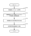
- FIG. 1 is a flowchart showing a method of manufacturing a light absorber according to an embodiment of the present invention. The method of manufacturing the light absorber will be described with reference to FIG.
- the resin substrate is irradiated with an ion beam (S100).
- a resin substrate for example, allyl diglycol carbonate resin (CR-39) is irradiated with an ion beam accelerated by a cyclotron.
- a large number of ion traces are formed in the vicinity of the surface of the resin substrate.
- the ion tracks are randomly distributed.
- an ion beam can use oxygen ion, being Ne ion and any of ions heavier than Ne ion makes it easy for etching to proceed selectively along the ion trace of the resin substrate, and the final Is preferable in that the basic pit aspect ratio (pit depth / pit radius) can be increased.
- the acceleration energy of the ion beam is preferably 200 MeV or more in that sufficient penetration depth can be obtained, and a large pit aspect ratio can be obtained even if the pit radius is made large.
- the irradiation density of the ion beam to the resin substrate is appropriately selected, but it is 1 ⁇ 10 5 / cm 2 to 1 ⁇ 10 6 / cm from the viewpoint of pit density sufficient to capture light of the far infrared wavelength. It is preferable that it is 2 .
- the resin substrate irradiated with the ion beam is etched with an alkaline solution to form an uneven surface on the surface (S110).
- the alkaline solution immerses the resin substrate irradiated with the ion beam for a predetermined time while heating to, for example, 70 ° C. using an aqueous solution of sodium hydroxide or potassium hydroxide. Then, the resin substrate is washed with water and dried.
- a transfer body is formed to cover the uneven surface of the etched resin substrate (S120).
- the transfer body is formed of, for example, a metal film, a photocurable resin, or silicone rubber.
- An uneven surface having a shape obtained by reversing the unevenness formed in S110 is formed on the transfer body.
- the transfer body is peeled off from the resin substrate to obtain a light absorber (S130).
- a light absorber S130
- the concavo-convex shape formed on the resin substrate is transferred, and a transfer body in which the reversed concavo-convex shape is formed is obtained.
- a metal film is formed as a transfer body in the above-described transfer body forming step (S120), for example, a vacuum evaporation method or a sputtering method is used to form an electrode layer for electroplating, for example, 100 nm to 500 nm thick.
- a metal film (single metal or alloy film) of copper (Cu), nickel (Ni), cobalt (Co) or the like is formed on the uneven surface of the resin substrate.
- a titanium (Ti) film may be formed to enhance adhesion.
- the electrode layer may be formed by electroless plating, and in order to improve the adhesion between the electrode layer and the resin substrate, the uneven surface of the resin substrate may be surface treated with a silane coupling agent. Then, using the electrode layer, a single metal or alloy such as Ni, chromium (Cr), Cu, gold (Au), silver (Ag), tin (Sn) or the like having a thickness of 100 ⁇ m to 1 mm by electroplating, Alternatively, an electroplated film is formed by laminating these. By peeling from the resin substrate in the peeling step (S130) described above, a light absorber of a transfer body of a metal film having a surface in which the uneven shape of the resin substrate is reversed is formed.
- a light absorber of a transfer body of a metal film having a surface in which the uneven shape of the resin substrate is reversed is formed.
- the uneven surface has high durability, heat resistance, and is free of binder.
- the electrode layer may be formed by an electroless plating method, a vacuum evaporation method, or the like, or a combination thereof. Also, the entire metal film may be formed by electroless plating.
- the ultraviolet curable resin is dropped and applied onto the uneven surface of the etched resin substrate. Cure. It is preferable to degas the ultraviolet curable resin before or after the dropping.
- the light absorber of the transfer body of the ultraviolet curable resin having the surface where the uneven shape of the resin substrate is reversed is formed.
- a silicone composition for example, a main agent and a curing agent of a two-component curable silicone composition mixed and etched
- the solution is applied dropwise to the uneven surface of the substrate and cured. It is preferable to degas the silicone composition before or after dropping (before curing).
- a light absorber of a silicone rubber transfer body having a surface in which the uneven shape of the resin substrate is reversed is formed.
- the concavo-convex shape formed on the resin substrate by ion beam irradiation and etching is transferred to the transfer body, and the material of the transfer body is, for example, metal film, photocuring
- the conductive resin and silicone rubber it has characteristics such as durability, mass productivity, low cost, etc. according to these materials, and as described in the examples described later, light with low reflectance is further used.
- Absorbers can be manufactured.
- a re-transfer body may be formed to cover the uneven surface of the transfer body.
- a retransferred body is formed of the above-described photocurable resin or silicone composition on the uneven surface of the above-described metal film, photocurable resin, or silicone rubber transfer body, the uneven shape is retransferred. Good.
- the metal film is excellent in durability, it can be used any number of times so that mass productivity is excellent.
- the above-described transfer process of the photocurable resin or silicone composition can be used.
- carbon powder such as carbon black or carbon nanotube may be mixed with the photocurable resin or silicone composition of the retransferred body.
- the reflectance in the ultraviolet to near infrared wavelength region can be reduced, and by mixing the carbon nanotube with the above-described material of the retransfer body, the above-described material of the retransfer body can be made to follow the uneven surface of the transfer body more. be able to.
- a light absorber having a remarkably low reflectance in the mid-infrared wavelength region as a light absorber having the uneven surface formed in S110 is described later. It can be manufactured.
- Example 1 A CR-39 resin substrate with 0.8 mm thickness (Product name Variotrac, manufactured by Fukubi Chemical Industries, Nagase Landauer Co., Ltd.), and using the AVF cyclotron at the Quantum Science and Technology R & D Organization Takasaki Quantum Research Institute for 260 MeV Irradiated with neon (Ne) ions.
- the irradiation density was set to 1 ⁇ 10 6 / cm 2 .
- the resin substrate irradiated with the ion beam is etched by being immersed in an aqueous solution of sodium hydroxide at 70 ° C. and 6.38N (N) for 9 hours, then washed with water and dried to form fine irregularities on the surface.
- the obtained resin substrate was obtained.
- an electrode layer for electroplating of a 50 nm-thick Ti film and a 300 nm-thick Cu film was formed on the uneven surface of the resin substrate by a sputtering method. Then, a 500 ⁇ m thick Ni plating film was formed as a transfer body on the electrode layer by electroplating.
- the Ni plating film was peeled off from the resin substrate to obtain a light absorber of the Ni plating film to which the unevenness was transferred.
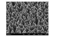
- FIG. 2 is an electron micrograph of the surface of the light absorber of Example 1. Referring to FIG. 2, on the surface of the light absorber of the Ni plating film, a large number of conical projections which decrease in diameter from the root toward the tip are distributed with the tips being separated from each other by several ⁇ m to several 10 ⁇ m. It is understood that it is forming.
- the electron micrograph is a scanning electron microscope (product name: JSM-7400F, acceleration voltage 1.5 kV) manufactured by JEOL Ltd., and the magnification is 1000 times.
- FIG. 3 is a diagram showing the total reflectance of the light absorber of Example 1. Referring to FIG. 3, it can be seen that in the light absorber of the Ni plating film, the total reflectance at wavelengths of 250 nm to 770 nm is reduced to 0.5% or less, and is 0.1% or more.
- the total reflectance is measured using a hemispherical total reflectance measurement unit (Spectralon integrating sphere) in a Perkin-Elmer UV-visible near-infrared spectrophotometer (product name LAMBDA 900), in the wavelength range of 250 nm to 750 nm. It measured at 10 nm intervals.
- a calibrated Specularon 99% standard reflector manufactured by Labsphere, Inc., product number SRS-99-020 was used.
- Example 2 In the same manner as in Example 1, an uneven surface was formed on the resin substrate of CR-39.
- a UV curable resin product name: Unisol Co., Ltd., product name: Unisola Soft
- a urethane acrylate resin and an epoxy acrylate resin is dropped and applied onto the uneven surface of the resin substrate to cover the surface and defoamed, CR-39.
- the ultraviolet curable resin was cured by irradiating ultraviolet light with a wavelength of 385 nm for 3 to 6 minutes with a UV light from the opposite side of the uneven surface of the resin substrate.
- the cured UV curable resin was peeled off from the resin substrate to obtain a light absorber of the UV cured resin to which the unevenness was transferred.
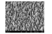
- FIG. 4 is an electron micrograph of the surface of the light absorber of Example 2. Referring to FIG. 4, on the surface of the light absorber of the ultraviolet curing resin, a large number of conical projections which decrease in diameter from the root toward the tip are distributed with the tips being separated from each other by several ⁇ m to several 10 ⁇ m. It is understood that it is forming. In addition, the electron microscope uses the same thing as Example 1, and magnification is 500 times.
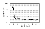
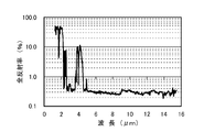
- FIG. 5 is a graph showing the total reflectance of the light absorber of Example 2. Referring to FIG. 5, in the light absorber of the ultraviolet curable resin, the total reflectance at a wavelength of 5 ⁇ m to 15 ⁇ m in the mid-infrared wavelength region is reduced to 0.5% or less, and 0.2% or more. It turns out that it has become.
- the total reflectance can be determined by using a hemispherical total reflectance measurement unit (gold-coated integrating sphere) in a Fourier transform infrared spectrometer (product name FT / IR-6300 type A) manufactured by JASCO Corporation. The range of 28 ⁇ m to 15.4 ⁇ m (wave number 650 cm -1 to 7800 cm -1 ) was measured at a wave number interval of 0.96 cm -1 . As a reference standard, a standard reflector with calibrated value (manufactured by US Labsphere, product name Infragold) was used.
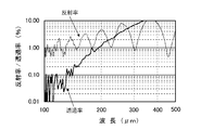
- FIG. 6 is a diagram showing the reflectance and the transmittance in the far-infrared wavelength region of the light absorber of Example 2.
- the light absorber of the ultraviolet curable resin has a reflectance of 1% or less at 100 ⁇ m in the far infrared wavelength region. Taking this into consideration and the fact that the total reflectance of the 5 ⁇ m to 15 ⁇ m wavelength in the mid-infrared wavelength region shown in FIG.
- the reflectance is 1% or less in the wavelength range of
- the light absorber of the ultraviolet curing resin has a transmittance of 0.1% or less at 100 ⁇ m in the far infrared wavelength region, the light absorptivity is 98.9% or more Is guessed.
- the reflectance and transmittance in the far infrared region were measured using a terahertz spectrometer (product name TR-1000) manufactured by Otsuka Electronics Co., Ltd., and the reflectance and transmittance of only the specular reflection component were measured.
- TR-1000 terahertz spectrometer manufactured by Otsuka Electronics Co., Ltd.
- Example 3 In the same manner as in Example 1, an uneven surface was formed on the resin substrate of CR-39.
- the main agent of a two-component curable silicone composition (Shin-Etsu Silicone main component SIM-360, curing agent CAT-360) and a curing agent are mixed at 9: 1, and after defoaming, the uneven surface of the resin substrate is formed.
- the solution was applied dropwise to cover the surface, and after defoaming in a vacuum desiccator, it was allowed to stand at room temperature for 12 hours to obtain a cured silicone rubber.
- the cured silicone rubber was peeled off from the resin substrate to obtain a light absorber of silicone rubber to which the unevenness was transferred.
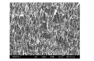
- FIG. 7 is an electron micrograph of the surface of the light absorber of Example 3. Referring to FIG. 7, on the surface of the light absorber of silicone rubber, a large number of conical projections having a diameter decreasing from the root toward the tip are formed with the tips being separated from each other by several ⁇ m to several 10 ⁇ m. I understand that I am doing. In addition, the electron microscope uses the same thing as Example 1, and magnification is 500 times.
- FIG. 8 is a graph showing the total reflectance of the light absorber of Example 3.
- the total reflectance at a wavelength of 5 ⁇ m to 15 ⁇ m in the mid-infrared wavelength region is reduced to 0.5% or less, and is 0.1% or more.
- the measurement condition of the total reflectance is the same as the measurement of FIG. 5 of the second embodiment.
- Example 4 In Example 4, using the light absorber of the Ni plating film of Example 1, a transfer body of the uneven surface was produced.
- the main agent of the two-component curable silicone composition (Shin-Etsu Silicone main component SIM-360, curing agent CAT-360) and the curing agent are mixed at 9: 1, and carbon black is further added to the silicone composition.
- the mixture was kneaded at 5 wt%, defoamed, drip-coated on the uneven surface of the Ni plating film to cover the surface, defoamed in a vacuum desiccator, and allowed to stand at room temperature for 12 hours to obtain a cured silicone rubber.
- the cured silicone rubber was peeled off from the Ni plating film to obtain a light absorber of carbon black-containing silicone rubber to which the unevenness was transferred.
- FIG. 9 is an electron micrograph of the surface of the light absorber of Example 4.
- a large number of projections in which a plurality of tips are connected in a ridge shape are formed, and the tips are separated from each other by several ⁇ m to several 10 ⁇ m. It can be seen that they are distributed and formed.
- the electron microscope uses the same thing as Example 1, and magnification is 500 times. Since this shape is similar to the shape shown in FIG. 11 of Example 5 described later, it can be inferred that it has at least the characteristics of low reflectance shown in FIG. 11, and it further contains carbon black. Therefore, low reflectance can be expected even in the ultraviolet to near infrared wavelength region.
- a resin substrate of CR-39 is irradiated with a neon (Ne) ion beam with an acceleration energy of 260 MeV at a density of 1 ⁇ 10 6 / cm 2 and then at 70 ° C .;
- This is a resin substrate obtained by immersing in a 38 N (N) aqueous solution of sodium hydroxide for etching for 9 hours, then washing with water and drying, and having fine irregularities formed on the surface.
- FIG. 10 is an electron micrograph of the surface of the light absorber of Example 5.
- a large number of projections in which a plurality of tips are connected in a ridge shape are formed, and the tips are distributed at intervals of several ⁇ m to several 10 ⁇ m. It can be seen that ridge-like continuous projections are formed and separated from each other by several ⁇ m to several tens of ⁇ m.
- the electron microscope uses the same thing as Example 1, and magnification is 500 times.
- FIG. 11 is a diagram showing the total reflectance of the light absorber of Example 5.
- the total reflectance of the wavelength of 5 ⁇ m to 15 ⁇ m in the mid-infrared wavelength region is reduced to 0.4% or less, and 0.2 It turns out that it is% or more.
- the measurement condition of the total reflectance is the same as the measurement of FIG. 5 of the second embodiment.
- Example measurement measurement of the total reflectance of the sample of the light absorber
- background measurement measurement of the background
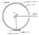
- FIG. 12 is a diagram for explaining the setting using the first sample port in the measurement of the total reflectance.
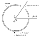
- FIG. 13 is a diagram for explaining setting of background measurement in the measurement of total reflectance.
- integrating sphere 10 is provided with a circular opening as a sample port for placing a measurement sample. .
- the sample port has an opening diameter of 20 mm (first sample port 11) and 30 mm (second sample port 12).
- the sample measurement is carried out by setting the measurement sample 13 in the first sample port 11 as shown in FIG.
- the measurement was made to be incident, and the background measurement was made to make the measurement light pass through the second sample port 12 as shown in FIG.
- the second sample port 12 is closed by the port plug 14 in the sample measurement (FIG. 12), and the first sample port 11 is closed by the port plug 15 in the background measurement.
- the sample measurement corresponding to the background measurement is not performed.
- the inventor of the present application notices that the total reflectance of the measurement sample is not properly obtained in FIG. 5 of the second embodiment, FIG. 8 of the third embodiment and FIG. 11 of the fifth embodiment. , And measured again.
- FIG. 14 is a diagram for explaining the setting using the second sample port in the measurement of the total reflectance.
- the measurement sample 13 was set to the second sample port 12 and the measurement was performed.
- the background measurement was performed such that the measurement light passes through the second sample port 12 in which the measurement sample 13 is not set.
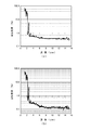
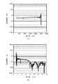
- FIG. 15 is a diagram for explaining the difference in measurement data due to the setting of measurement of the total reflectance.
- FIG. 15 (a) shows data obtained when sample measurement is performed in the arrangement shown in FIG. 12, and
- FIG. 15 (b) shows data obtained when sample measurement is performed in the arrangement shown in FIG. Show.
- the light absorber of Example 5 shown above is used as a measurement sample, Moreover, it is the data which is not processed except a background, and it is what is called raw data.
- Total reflectance obtained by sample measurement by second sample port 12 and background measurement The sample measurement was set in the second sample port 12 and the measurement was performed, and the background measurement was obtained by passing the measurement light through the second sample port 12 in which the measurement sample 13 was not set. Indicates total reflectance.
- the measurement sample is the same as the sample used in each of the previous examples, and the measurement apparatus is the same as the measurement apparatus described in FIG. 5 (Example 2).
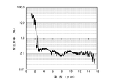
- FIG. 16 is a diagram showing the total reflectance (using a second sample port) of the light absorber of Example 2 of the present invention.
- the total reflectance of a wavelength of 3 ⁇ m to 15 ⁇ m in the mid-infrared wavelength region is 0.3% or less, and 0.02% or more. It is understood that
- FIG. 17 is a diagram showing the total reflectance (using the second sample port) of the light absorber of Example 3 of the present invention.
- the total reflectance of the wavelength of 5.5 ⁇ m to 15 ⁇ m in the mid-infrared wavelength region is 0.2% or less, and 0.001% It turns out that it is above.
- FIG. 18 is a diagram showing the total reflectance on the short wavelength side of the light absorber in Example 4 of the present invention and the total reflectance on the long wavelength side (using the second sample port) on the short wavelength side.
- the light absorber of Example 4 is obtained by covering the uneven surface of the light absorber of the Ni plating film of Example 1 with the carbon black-containing silicone composition and removing it after curing. It is a transfer body made of silicone rubber and has the surface shown in the electron micrograph of FIG. Referring to FIG. 18A, the light absorber of the carbon black-containing silicone rubber of Example 4 has a total reflectance of 250 nm (0.25 ⁇ m) to 2400 nm (2.4 ⁇ m) in the wavelength range of ultraviolet to near infrared light.
- the light absorber of the carbon black-containing silicone rubber of Example 4 has a total reflectance of 0.4% or less at a wavelength of 2 ⁇ m to 15 ⁇ m in the wavelength region of mid-infrared light, It turns out that it is 0.001% or more.
- the total reflectance of 0.25 ⁇ m to 2.4 ⁇ m in the ultraviolet to near infrared wavelength region is a hemispherical total reflectance measurement unit (Spectra) in a UV-visible near-infrared spectrophotometer (product name LAMBDA 900) manufactured by PerkinElmer. Long integrating spheres) were used and measured at wavelength intervals of 10 nm.
- a calibrated Specularon 99% standard reflector manufactured by Labsphere, Inc., product number SRS-99-020 was used.
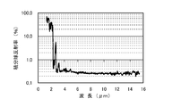
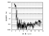
- FIG. 19 is a diagram showing the total reflectance (using a second sample port) of the light absorber of Example 5 of the present invention.
- the light absorber of the resin substrate of Example 5 has a total reflectance of 0.1% or less and 0.001% or more at a wavelength of 4 ⁇ m to 15 ⁇ m in the mid-infrared wavelength region. I know that there is.
- the light absorber manufactured by the manufacturing method according to the embodiment of the present invention may be a thermography for plant monitoring or heat generation person detection, an on-vehicle pedestrian night vision device, an infrared ray for night security, watching etc. It can be used in a wide range of applications such as sensors and infrared sensors for earth observation (remote sensing), and can easily be enlarged, so the main radiation wavelength range at ordinary temperature range, for example, (3 ⁇ m to 100 ⁇ m Can be used as a flat black body standard with an emissivity of almost 100% in the wavelength range of.
- a method for producing a light absorber A first step of irradiating the resin substrate with an ion beam; A second step of etching the irradiated resin substrate with an alkaline solution to form an uneven surface on the surface; A third step of forming a transfer body covering the uneven surface of the etched resin substrate; A fourth step of peeling the transfer body from the resin substrate to obtain a light absorber; Said manufacturing method including.
- the resin substrate is allyl diglycol carbonate resin (CR-39),
- the ion beam uses either Ne ions or ions heavier than Ne ions,
- the alkaline solution has strong alkalinity,
- the transfer body is a photocurable resin obtained by applying a photocurable resin to the concavo-convex surface of the etched resin substrate and curing by light irradiation. The manufacturing method according to any one of the above.
Landscapes
- Physics & Mathematics (AREA)
- Engineering & Computer Science (AREA)
- Mechanical Engineering (AREA)
- General Physics & Mathematics (AREA)
- Optics & Photonics (AREA)
- Manufacturing & Machinery (AREA)
- Health & Medical Sciences (AREA)
- Inorganic Chemistry (AREA)
- Chemical & Material Sciences (AREA)
- Ophthalmology & Optometry (AREA)
- Toxicology (AREA)
- Laminated Bodies (AREA)
- Optical Elements Other Than Lenses (AREA)
- Blocking Light For Cameras (AREA)
- Surface Treatment Of Optical Elements (AREA)
- Paints Or Removers (AREA)
- Optical Filters (AREA)
Abstract
Description
厚さ0.8mmのCR-39の樹脂基板(製品名バリオトラック、フクビ化学工業社製、長瀬ランダウア社販売)に、量子科学技術研究開発機構 高崎量子応用研究所のAVFサイクロトロンにより加速エネルギー260MeVのネオン(Ne)イオンを照射した。照射密度は1×10⁶/cm2に設定した。
実施例1と同様にして、CR-39の樹脂基板に凹凸面を形成した。
実施例1と同様にして、CR-39の樹脂基板に凹凸面を形成した。
実施例4は、実施例1のNiめっき膜の光吸収体を用いて、その凹凸面の転写体を作製した。
実施例5は、実施例1と同様に、CR-39の樹脂基板に加速エネルギー260MeVのネオン(Ne)イオンビームを1×10⁶/cm2の密度で照射し、次いで、70℃、6.38規定(N)の水酸化ナトリウム水溶液に9時間浸漬してエッチングを行い、その後水洗および乾燥して得た、表面に微細な凹凸が形成された樹脂基板である。
以下、サンプル測定を第2サンプルポート12にセットして測定を行い、バックグラウンド測定は、測定サンプル13をセットしていない第2サンプルポート12を測定光が通過するようにして行って得られた全反射率を示す。測定サンプルは先の各実施例で使用したサンプルと同一であり、測定装置は先の図5(実施例2)で述べた測定装置と同一である。
(付記1) 光吸収体の製造方法であって、
樹脂基板にイオンビームを照射する第1のステップと、
前記照射された樹脂基板をアルカリ溶液でエッチングしてその表面に凹凸面を形成する第2のステップと、
前記エッチングした樹脂基板の凹凸面を覆う転写体を形成する第3のステップと、
前記転写体を前記樹脂基板から剥離して光吸収体を得る第4のステップと、
を含む、前記製造方法。
(付記2) 前記樹脂基板はアリルジグリコールカーボネート樹脂(CR-39)であり、
前記イオンビームはNeイオンとNeイオンよりも重いイオンのうちいずれかを用い、
前記アルカリ溶液は強アルカリ性を有する、
付記1記載の製造方法。
(付記3) 前記イオンビームは加速エネルギーが200MeV以上である、付記1または2記載の製造方法。
(付記4) 前記第3のステップにおいて、前記転写体は、前記エッチングした樹脂基板の凹凸面に形成した金属膜である、付記1~3のうちいずれか一項記載の製造方法。
(付記5) 前記金属膜の光吸収体は、250nm~770nmの波長の全反射率が、0.5%以下である表面が形成される、付記4記載の製造方法。
(付記6) 前記金属膜の光吸収体は、250nm~770nmの波長の全反射率が、0.1%以上である表面が形成される、付記5記載の製造方法。
(付記7) 前記第3のステップにおいて、前記転写体は、前記エッチングした樹脂基板の凹凸面に光硬化性樹脂を塗布し、光照射により硬化させた光硬化性樹脂である、付記1~3のうちいずれか一項記載の製造方法。
(付記8) 前記光硬化性樹脂の光吸収体は、5μm~15μmの波長の全反射率が、0.5%以下である表面が形成される、付記7記載の製造方法。
(付記9) 前記光硬化性樹脂の光吸収体は、5μm~15μmの波長の全反射率が、0.2%以上である表面が形成される、付記8記載の製造方法。
(付記10) 前記光硬化性樹脂の光吸収体は、3μm~15μmの波長の全反射率が、0.3%以下である表面が形成される、付記7記載の製造方法。
(付記11) 前記光硬化性樹脂の光吸収体は、3μm~15μmの波長の全反射率が、0.02%以上である表面が形成される、付記10記載の製造方法。
(付記12) 前記第3のステップにおいて、前記転写体は、前記エッチングした樹脂基板の凹凸面にシリコーン組成物を塗布し、硬化したシリコーンゴムである、付記1~3のうちいずれか一項記載の製造方法。
(付記13) 前記シリコーンゴムの光吸収体は、5μm~15μmの波長の全反射率が、0.5%以下である表面が形成される、付記12記載の製造方法。
(付記14) 前記シリコーンゴムの光吸収体は、5μm~15μmの波長の全反射率が、0.1%以上である表面が形成される、付記13記載の製造方法。
(付記15) 前記シリコーンゴムの光吸収体は、5.5μm~15μmの波長の全反射率が、0.2%以下である表面が形成される、付記12記載の製造方法。
(付記16) 前記シリコーンゴムの光吸収体は、5.5μm~15μmの波長の全反射率が、0.001%以上である表面が形成される、付記15記載の製造方法。
(付記17) 前記第4のステップにおいて得られた前記転写体の凹凸面を覆う再転写体を形成する第5のステップと、
前記再転写体を前記転写体から剥離して光吸収体を得る第6のステップと、
をさらに含む、付記1~16のうちいずれか一項記載の製造方法。
(付記18) 前記第5のステップにおいて、前記再転写体は、カーボン粉体を分散させたシリコーン組成物を塗布し、硬化したシリコーンゴムである、付記17記載の製造方法。
(付記19) 前記カーボン粉体を分散させたシリコーンゴムの光吸収体は、0.25μm~2.4μmの波長の全反射率が、0.6%以下である表面が形成される、付記18記載の製造方法。
(付記20) 前記カーボン粉体を分散させたシリコーンゴムの光吸収体は、0.25μm~2.4μmの波長の全反射率が、0.2%以上である表面が形成される、付記19記載の製造方法。
(付記21) 前記カーボン粉体を分散させたシリコーンゴムの光吸収体は、2μm~15μmの波長の全反射率が、0.4%以下である表面が形成される、付記18記載の製造方法。
(付記22) 前記カーボン粉体を分散させたシリコーンゴムの光吸収体は、2μm~15μmの波長の全反射率が、0.001%以上である表面が形成される、付記21記載の製造方法。
(付記23) 光吸収体の製造方法であって、
樹脂基板にイオンビームを照射する第1のステップと、
前記照射された樹脂基板の表面をアルカリ溶液でエッチングする第2のステップと、を含み、
前記第1および第2のステップにより、前記樹脂基板に、5μm~15μmの波長の全反射率が0.4%以下である凹凸面を形成させる、前記製造方法。
(付記24) 前記樹脂基板は、5μm~15μmの波長の全反射率が0.2%以上である、付記23記載の製造方法。
(付記25) 光吸収体の製造方法であって、
樹脂基板にイオンビームを照射する第1のステップと、
前記照射された樹脂基板の表面をアルカリ溶液でエッチングする第2のステップと、を含み、
前記第1および第2のステップにより、前記樹脂基板に、4μm~15μmの波長の全反射率が0.1%以下である凹凸面を形成させる、前記製造方法。
(付記26) 前記樹脂基板は、4μm~15μmの波長の全反射率が0.001%以上である、付記25記載の製造方法。
(付記27) 前記樹脂基板はアリルジグリコールカーボネート樹脂(CR-39)であり、
前記アルカリ溶液は強アルカリ性を有し、
前記イオンビームはNeイオンとNeイオンよりも重いイオンのうちいずれかを用いる、付記23~26のうちいずれか一項記載の製造方法。
(付記28) 前記イオンビームは加速エネルギーが200MeV以上である、付記23~27のうちいずれか一項記載の製造方法。
Claims (13)
- 光吸収体の製造方法であって、
樹脂基板にイオンビームを照射する第1のステップと、
前記照射された樹脂基板をアルカリ溶液でエッチングしてその表面に凹凸面を形成する第2のステップと、
前記エッチングした樹脂基板の凹凸面を覆う転写体を形成する第3のステップと、
前記転写体を前記樹脂基板から剥離して光吸収体を得る第4のステップと、
を含む、前記製造方法。 - 前記樹脂基板はアリルジグリコールカーボネート樹脂(CR-39)であり、
前記イオンビームはNeイオンとNeイオンよりも重いイオンのうちいずれかを用い、
前記アルカリ溶液は強アルカリ性を有する、
請求項1記載の製造方法。 - 前記イオンビームは加速エネルギーが200MeV以上である、請求項1または2記載の製造方法。
- 前記第3のステップにおいて、前記転写体は、前記エッチングした樹脂基板の凹凸面に形成した金属膜である、請求項1~3のうちいずれか一項記載の製造方法。
- 前記金属膜の光吸収体は、250nm~770nmの波長の全反射率が、0.5%以下である表面が形成される、請求項4記載の製造方法。
- 前記第3のステップにおいて、前記転写体は、前記エッチングした樹脂基板の凹凸面に光硬化性樹脂を塗布し、光照射により硬化させた光硬化性樹脂である、請求項1~3のうちいずれか一項記載の製造方法。
- 前記光硬化性樹脂の光吸収体は、3μm~15μmの波長の全反射率が、0.3%以下である表面が形成される、請求項6記載の製造方法。
- 前記第3のステップにおいて、前記転写体は、前記エッチングした樹脂基板の凹凸面にシリコーン組成物を塗布し、硬化したシリコーンゴムである、請求項1~3のうちいずれか一項記載の製造方法。
- 前記シリコーンゴムの光吸収体は、5.5μm~15μmの波長の全反射率が、0.2%以下である表面が形成される、請求項8記載の製造方法。
- 前記第4のステップにおいて得られた前記転写体の凹凸面を覆う再転写体を形成する第5のステップと、
前記再転写体を前記転写体から剥離して光吸収体を得る第6のステップと、
をさらに含む、請求項1~9のうちいずれか一項記載の製造方法。 - 前記第5のステップにおいて、前記再転写体は、カーボン粉体を分散させたシリコーン組成物を塗布し、硬化したシリコーンゴムであり、前記カーボン粉体を分散させたシリコーンゴムの光吸収体は、0.25μm~2.4μmの波長の全反射率が0.6%以下、かつ2μm~15μmの波長の全反射率が0.4%以下である表面が形成される、請求項10記載の製造方法。
- 光吸収体の製造方法であって、
樹脂基板にイオンビームを照射する第1のステップと、
前記照射された樹脂基板の表面をアルカリ溶液でエッチングする第2のステップと、を含み、
前記第1および第2のステップにより、前記樹脂基板に、4μm~15μmの波長の全反射率が0.1%以下である凹凸面を形成させる、前記製造方法。 - 前記樹脂基板はアリルジグリコールカーボネート樹脂(CR-39)であり、
前記アルカリ溶液は強アルカリ性を有し、
前記イオンビームはNeイオンとNeイオンよりも重いイオンのうちいずれかを用いる、請求項12記載の製造方法。
Priority Applications (5)
| Application Number | Priority Date | Filing Date | Title |
|---|---|---|---|
| CN201880071321.7A CN111295602B (zh) | 2017-11-02 | 2018-05-09 | 光吸收体的制造方法 |
| US16/760,712 US11565488B2 (en) | 2017-11-02 | 2018-05-09 | Method for manufacturing light absorber |
| EP18873053.5A EP3699649B1 (en) | 2017-11-02 | 2018-05-09 | Method for manufacturing light absorber |
| JP2019549826A JP6961255B2 (ja) | 2017-11-02 | 2018-05-09 | 光吸収体の製造方法 |
| KR1020207010649A KR102376865B1 (ko) | 2017-11-02 | 2018-05-09 | 광 흡수체의 제조 방법 |
Applications Claiming Priority (2)
| Application Number | Priority Date | Filing Date | Title |
|---|---|---|---|
| JP2017212380 | 2017-11-02 | ||
| JP2017-212380 | 2017-11-02 |
Publications (1)
| Publication Number | Publication Date |
|---|---|
| WO2019087439A1 true WO2019087439A1 (ja) | 2019-05-09 |
Family
ID=66331533
Family Applications (1)
| Application Number | Title | Priority Date | Filing Date |
|---|---|---|---|
| PCT/JP2018/017949 Ceased WO2019087439A1 (ja) | 2017-11-02 | 2018-05-09 | 光吸収体の製造方法 |
Country Status (6)
| Country | Link |
|---|---|
| US (1) | US11565488B2 (ja) |
| EP (1) | EP3699649B1 (ja) |
| JP (1) | JP6961255B2 (ja) |
| KR (1) | KR102376865B1 (ja) |
| CN (1) | CN111295602B (ja) |
| WO (1) | WO2019087439A1 (ja) |
Cited By (3)
| Publication number | Priority date | Publication date | Assignee | Title |
|---|---|---|---|---|
| JPWO2022050061A1 (ja) * | 2020-09-04 | 2022-03-10 | ||
| WO2022181259A1 (ja) * | 2021-02-24 | 2022-09-01 | 国立研究開発法人産業技術総合研究所 | 赤外線吸収体、その製造方法、黒体輻射装置および放射冷却装置 |
| US11852848B2 (en) | 2019-11-29 | 2023-12-26 | Largan Precision Co., Ltd. | Imaging lens assembly, camera module and electronic device |
Families Citing this family (7)
| Publication number | Priority date | Publication date | Assignee | Title |
|---|---|---|---|---|
| JP6592211B1 (ja) * | 2019-02-20 | 2019-10-16 | 河西工業株式会社 | 成形用金型、成形用金型の製造方法、射出成形装置及び成形品の製造方法 |
| DE102019123404B4 (de) * | 2019-09-02 | 2024-02-15 | Bayerische Motoren Werke Aktiengesellschaft | Sensorvorrichtung und Fahrassistenzsystem |
| EP4135972A1 (en) * | 2020-04-14 | 2023-02-22 | Essilor International | Method for producing a mold |
| CN112675822B (zh) * | 2020-11-26 | 2021-07-20 | 哈尔滨工业大学 | 一种高吸收高发射率超黑分子吸附涂层的制备方法 |
| CN113640906A (zh) * | 2021-07-09 | 2021-11-12 | 中国科学院近代物理研究所 | 一种近完美光吸收体及其普适性的制备方法 |
| CN114672184A (zh) * | 2022-05-27 | 2022-06-28 | 华侨大学 | 一种超黑光吸收涂层及其制备方法和应用 |
| CN118584569B (zh) * | 2024-07-22 | 2024-11-01 | 中国科学院近代物理研究所 | 金属纳米锥管等离激元共振腔、制备方法及其应用 |
Citations (2)
| Publication number | Priority date | Publication date | Assignee | Title |
|---|---|---|---|---|
| JP2008233850A (ja) * | 2006-08-09 | 2008-10-02 | Tokyo Univ Of Science | 反射防止構造体及びその製造方法並びに光学部材の製造方法 |
| JP2017032806A (ja) * | 2015-08-03 | 2017-02-09 | 国立大学法人東京工業大学 | 反射防止用微細突起の製造方法 |
Family Cites Families (4)
| Publication number | Priority date | Publication date | Assignee | Title |
|---|---|---|---|---|
| JP2007304466A (ja) * | 2006-05-15 | 2007-11-22 | Matsushita Electric Ind Co Ltd | 光吸収性反射防止構造体、それを備えた光学ユニット及びレンズ鏡筒ユニット、並びにそれらを備えた光学装置 |
| JP4269295B2 (ja) * | 2007-02-20 | 2009-05-27 | セイコーエプソン株式会社 | 微細構造体の製造方法 |
| JP5536437B2 (ja) | 2009-12-22 | 2014-07-02 | スタンレー電気株式会社 | 光強度測定装置及びその製造方法 |
| JP2012189846A (ja) * | 2011-03-11 | 2012-10-04 | Tamron Co Ltd | 反射防止光学素子及び反射防止光学素子の製造方法 |
-
2018
- 2018-05-09 WO PCT/JP2018/017949 patent/WO2019087439A1/ja not_active Ceased
- 2018-05-09 KR KR1020207010649A patent/KR102376865B1/ko active Active
- 2018-05-09 CN CN201880071321.7A patent/CN111295602B/zh active Active
- 2018-05-09 EP EP18873053.5A patent/EP3699649B1/en active Active
- 2018-05-09 US US16/760,712 patent/US11565488B2/en active Active
- 2018-05-09 JP JP2019549826A patent/JP6961255B2/ja active Active
Patent Citations (3)
| Publication number | Priority date | Publication date | Assignee | Title |
|---|---|---|---|---|
| JP2008233850A (ja) * | 2006-08-09 | 2008-10-02 | Tokyo Univ Of Science | 反射防止構造体及びその製造方法並びに光学部材の製造方法 |
| JP5177581B2 (ja) | 2006-08-09 | 2013-04-03 | 学校法人東京理科大学 | 反射防止構造体の製造方法 |
| JP2017032806A (ja) * | 2015-08-03 | 2017-02-09 | 国立大学法人東京工業大学 | 反射防止用微細突起の製造方法 |
Non-Patent Citations (3)
| Title |
|---|
| AMEMIYA, KUNIAKI ET AL.: "Fabrication of hard- coated optical absorbers with microstructured surfaces using etched ion tracks: toward broadband ultra-low reflectance", NUCLEAR INSTRUMENTS AND METHODS IN PHYSICS RESEARCH B, vol. 356, no. 357, 2015, pages 154 - 159, XP029246393, DOI: doi:10.1016/j.nimb.2015.05.002 * |
| KUNIAKI AMEMIYA: "Fabrication of hard-coated optical absorbers with microstructured surfaces using etched ion tracks: toward broadband ultra-low reflectance", NUCLEAR INSTRUMENTS AND METHODS IN PHYSICS RESEARCH B, vol. 356, no. 357, 2015, pages 154 - 159, XP029246393, DOI: 10.1016/j.nimb.2015.05.002 |
| See also references of EP3699649A4 |
Cited By (11)
| Publication number | Priority date | Publication date | Assignee | Title |
|---|---|---|---|---|
| US11852848B2 (en) | 2019-11-29 | 2023-12-26 | Largan Precision Co., Ltd. | Imaging lens assembly, camera module and electronic device |
| US12429633B2 (en) | 2019-11-29 | 2025-09-30 | Largan Precision Co., Ltd. | Imaging lens assembly, camera module and electronic device |
| US12436320B2 (en) | 2019-11-29 | 2025-10-07 | Largan Precision Co., Ltd. | Imaging lens assembly, camera module and electronic device |
| JPWO2022050061A1 (ja) * | 2020-09-04 | 2022-03-10 | ||
| WO2022050061A1 (ja) | 2020-09-04 | 2022-03-10 | 国立研究開発法人産業技術総合研究所 | 光吸収体およびその製造方法 |
| JP7655571B2 (ja) | 2020-09-04 | 2025-04-02 | 国立研究開発法人産業技術総合研究所 | 光吸収体およびその製造方法 |
| WO2022181259A1 (ja) * | 2021-02-24 | 2022-09-01 | 国立研究開発法人産業技術総合研究所 | 赤外線吸収体、その製造方法、黒体輻射装置および放射冷却装置 |
| JPWO2022181259A1 (ja) * | 2021-02-24 | 2022-09-01 | ||
| US20240125518A1 (en) * | 2021-02-24 | 2024-04-18 | National Institute Of Advanced Industrial Science And Technology | Infrared absorber, method for manufacturing same, black-body radiation device, and radiative cooling device |
| JP7598673B2 (ja) | 2021-02-24 | 2024-12-12 | 国立研究開発法人産業技術総合研究所 | 赤外線吸収体、その製造方法、黒体輻射装置および放射冷却装置 |
| US12498144B2 (en) * | 2021-02-24 | 2025-12-16 | National Institute Of Advanced Industrial Science And Technology | Infrared absorber, method for manufacturing same, blackbody radiation device, and radiative cooling device |
Also Published As
| Publication number | Publication date |
|---|---|
| EP3699649A4 (en) | 2020-12-30 |
| JPWO2019087439A1 (ja) | 2020-08-27 |
| US20200346421A1 (en) | 2020-11-05 |
| CN111295602A (zh) | 2020-06-16 |
| KR102376865B1 (ko) | 2022-03-18 |
| US11565488B2 (en) | 2023-01-31 |
| CN111295602B (zh) | 2022-03-29 |
| EP3699649A1 (en) | 2020-08-26 |
| EP3699649B1 (en) | 2022-06-22 |
| JP6961255B2 (ja) | 2021-11-05 |
| KR20200054257A (ko) | 2020-05-19 |
Similar Documents
| Publication | Publication Date | Title |
|---|---|---|
| JP6961255B2 (ja) | 光吸収体の製造方法 | |
| Kook et al. | Fabrication of highly dense silk fibroin biomemristor array and its resistive switching characteristics | |
| Li et al. | Transparent selective photothermal coatings for antifogging applications | |
| Wang et al. | Highly reliable silver nanowire transparent electrode employing selectively patterned barrier shaped by self-masked photolithography | |
| US20190202689A1 (en) | Highly stretchable three-dimensional percolated conductive nano-network structure, method of manufacturing the same, strain sensor including the same and wearable device including the same | |
| US20160028327A1 (en) | Method of producing a triboelectric generator with rough dielectric polymer | |
| KR101237052B1 (ko) | 그라핀 세포 자극기 및 그것의 제조방법 | |
| WO2014175163A1 (ja) | 導電パターンの製造方法及び導電パターン形成基板 | |
| JP2017088785A (ja) | 導電性フィルム | |
| Fang et al. | Femtosecond laser structuring for flexible surface-enhanced Raman spectroscopy substrates | |
| Zhang et al. | High-resolution stretchable soft liquid metal circuits based on cu–Ga alloying and femtosecond laser ablation | |
| Koschinski et al. | Validation of transparent and flexible neural implants for simultaneous electrophysiology, functional imaging, and optogenetics | |
| Kim et al. | Silver Nanowires Network Film with Enhanced Crystallinity toward Mechano‐Electrically Sustainable Flexible‐Electrode | |
| KR102610916B1 (ko) | 농도구배 구조를 가지는 유연 압력센서 제조 방법 | |
| JP7655571B2 (ja) | 光吸収体およびその製造方法 | |
| US12498144B2 (en) | Infrared absorber, method for manufacturing same, blackbody radiation device, and radiative cooling device | |
| Sun et al. | Laser-assisted preparation of flexible wearable electronics with copper-liquid metal patterns | |
| JP2016212986A (ja) | 伸縮性導電フィルムおよび伸縮性導電フィルムの製造方法 | |
| US20220153946A1 (en) | Method of manufacturing flexible pressure sensor having concentration gradation profile | |
| Yang et al. | Multifunctional pressure/strain sensor based on dual-layer Mxene/TiO 2/TPU and its application in gesture recognition | |
| CN116507140A (zh) | 离子凝胶光探测与神经形态视觉传感器及其制备方法 | |
| Zhang et al. | Optoelectronic synapse based on 2D metal-organic framework Cu3 (HHTP) 2 for neuromorphic processing of both visual and auditory information | |
| JP2014522546A (ja) | 透明な構成要素の改良および透明な構成要素に関する改良 | |
| Choi et al. | Intelligent Motion Detector: Compositing Reversibly-Crosslinkable Polymer Films with Encapsulated Electrodes and Cognitive Convolutional Neural Networks | |
| KR102050295B1 (ko) | 3차원 인터커넥트 패턴을 포함한 스마트 렌즈를 제조하는 방법 및 상기 방법에 의해 제조된 스마트 렌즈 |
Legal Events
| Date | Code | Title | Description |
|---|---|---|---|
| 121 | Ep: the epo has been informed by wipo that ep was designated in this application |
Ref document number: 18873053 Country of ref document: EP Kind code of ref document: A1 |
|
| ENP | Entry into the national phase |
Ref document number: 2019549826 Country of ref document: JP Kind code of ref document: A |
|
| ENP | Entry into the national phase |
Ref document number: 20207010649 Country of ref document: KR Kind code of ref document: A |
|
| NENP | Non-entry into the national phase |
Ref country code: DE |
|
| ENP | Entry into the national phase |
Ref document number: 2018873053 Country of ref document: EP Effective date: 20200518 |