WO2019087471A1 - 固体撮像素子 - Google Patents
固体撮像素子 Download PDFInfo
- Publication number
- WO2019087471A1 WO2019087471A1 PCT/JP2018/026757 JP2018026757W WO2019087471A1 WO 2019087471 A1 WO2019087471 A1 WO 2019087471A1 JP 2018026757 W JP2018026757 W JP 2018026757W WO 2019087471 A1 WO2019087471 A1 WO 2019087471A1
- Authority
- WO
- WIPO (PCT)
- Prior art keywords
- chip
- solid
- circuit
- imaging device
- state imaging
- Prior art date
- Legal status (The legal status is an assumption and is not a legal conclusion. Google has not performed a legal analysis and makes no representation as to the accuracy of the status listed.)
- Ceased
Links
Images









Classifications
-
- H—ELECTRICITY
- H04—ELECTRIC COMMUNICATION TECHNIQUE
- H04N—PICTORIAL COMMUNICATION, e.g. TELEVISION
- H04N25/00—Circuitry of solid-state image sensors [SSIS]; Control thereof
- H04N25/70—SSIS architectures; Circuits associated therewith
- H04N25/79—Arrangements of circuitry being divided between different or multiple substrates, chips or circuit boards, e.g. stacked image sensors
-
- H—ELECTRICITY
- H04—ELECTRIC COMMUNICATION TECHNIQUE
- H04N—PICTORIAL COMMUNICATION, e.g. TELEVISION
- H04N25/00—Circuitry of solid-state image sensors [SSIS]; Control thereof
- H04N25/70—SSIS architectures; Circuits associated therewith
- H04N25/76—Addressed sensors, e.g. MOS or CMOS sensors
-
- H—ELECTRICITY
- H04—ELECTRIC COMMUNICATION TECHNIQUE
- H04N—PICTORIAL COMMUNICATION, e.g. TELEVISION
- H04N25/00—Circuitry of solid-state image sensors [SSIS]; Control thereof
- H04N25/47—Image sensors with pixel address output; Event-driven image sensors; Selection of pixels to be read out based on image data
-
- H—ELECTRICITY
- H04—ELECTRIC COMMUNICATION TECHNIQUE
- H04N—PICTORIAL COMMUNICATION, e.g. TELEVISION
- H04N25/00—Circuitry of solid-state image sensors [SSIS]; Control thereof
- H04N25/70—SSIS architectures; Circuits associated therewith
-
- H—ELECTRICITY
- H04—ELECTRIC COMMUNICATION TECHNIQUE
- H04N—PICTORIAL COMMUNICATION, e.g. TELEVISION
- H04N25/00—Circuitry of solid-state image sensors [SSIS]; Control thereof
- H04N25/70—SSIS architectures; Circuits associated therewith
- H04N25/703—SSIS architectures incorporating pixels for producing signals other than image signals
- H04N25/704—Pixels specially adapted for focusing, e.g. phase difference pixel sets
-
- H—ELECTRICITY
- H04—ELECTRIC COMMUNICATION TECHNIQUE
- H04N—PICTORIAL COMMUNICATION, e.g. TELEVISION
- H04N25/00—Circuitry of solid-state image sensors [SSIS]; Control thereof
- H04N25/70—SSIS architectures; Circuits associated therewith
- H04N25/703—SSIS architectures incorporating pixels for producing signals other than image signals
- H04N25/707—Pixels for event detection
-
- H—ELECTRICITY
- H04—ELECTRIC COMMUNICATION TECHNIQUE
- H04N—PICTORIAL COMMUNICATION, e.g. TELEVISION
- H04N25/00—Circuitry of solid-state image sensors [SSIS]; Control thereof
- H04N25/70—SSIS architectures; Circuits associated therewith
- H04N25/76—Addressed sensors, e.g. MOS or CMOS sensors
- H04N25/766—Addressed sensors, e.g. MOS or CMOS sensors comprising control or output lines used for a plurality of functions, e.g. for pixel output, driving, reset or power
-
- H—ELECTRICITY
- H04—ELECTRIC COMMUNICATION TECHNIQUE
- H04N—PICTORIAL COMMUNICATION, e.g. TELEVISION
- H04N25/00—Circuitry of solid-state image sensors [SSIS]; Control thereof
- H04N25/70—SSIS architectures; Circuits associated therewith
- H04N25/76—Addressed sensors, e.g. MOS or CMOS sensors
- H04N25/77—Pixel circuitry, e.g. memories, A/D converters, pixel amplifiers, shared circuits or shared components
-
- H—ELECTRICITY
- H04—ELECTRIC COMMUNICATION TECHNIQUE
- H04N—PICTORIAL COMMUNICATION, e.g. TELEVISION
- H04N25/00—Circuitry of solid-state image sensors [SSIS]; Control thereof
- H04N25/70—SSIS architectures; Circuits associated therewith
- H04N25/76—Addressed sensors, e.g. MOS or CMOS sensors
- H04N25/77—Pixel circuitry, e.g. memories, A/D converters, pixel amplifiers, shared circuits or shared components
- H04N25/772—Pixel circuitry, e.g. memories, A/D converters, pixel amplifiers, shared circuits or shared components comprising A/D, V/T, V/F, I/T or I/F converters
-
- H—ELECTRICITY
- H10—SEMICONDUCTOR DEVICES; ELECTRIC SOLID-STATE DEVICES NOT OTHERWISE PROVIDED FOR
- H10F—INORGANIC SEMICONDUCTOR DEVICES SENSITIVE TO INFRARED RADIATION, LIGHT, ELECTROMAGNETIC RADIATION OF SHORTER WAVELENGTH OR CORPUSCULAR RADIATION
- H10F39/00—Integrated devices, or assemblies of multiple devices, comprising at least one element covered by group H10F30/00, e.g. radiation detectors comprising photodiode arrays
- H10F39/80—Constructional details of image sensors
- H10F39/802—Geometry or disposition of elements in pixels, e.g. address-lines or gate electrodes
- H10F39/8027—Geometry of the photosensitive area
-
- H—ELECTRICITY
- H10—SEMICONDUCTOR DEVICES; ELECTRIC SOLID-STATE DEVICES NOT OTHERWISE PROVIDED FOR
- H10F—INORGANIC SEMICONDUCTOR DEVICES SENSITIVE TO INFRARED RADIATION, LIGHT, ELECTROMAGNETIC RADIATION OF SHORTER WAVELENGTH OR CORPUSCULAR RADIATION
- H10F39/00—Integrated devices, or assemblies of multiple devices, comprising at least one element covered by group H10F30/00, e.g. radiation detectors comprising photodiode arrays
- H10F39/80—Constructional details of image sensors
- H10F39/809—Constructional details of image sensors of hybrid image sensors
Definitions
- the present technology relates to a solid-state imaging device. Specifically, the present invention relates to a solid-state imaging device that compares the amount of incident light with a threshold.
- synchronous solid-state imaging devices that capture image data (frames) in synchronization with synchronization signals such as vertical synchronization signals are used in imaging devices and the like.
- image data can be acquired only for each cycle of the synchronization signal (for example, 1/60 seconds), so faster processing is possible in the fields related to traffic, robots, etc. It will be difficult to respond when requested. Therefore, an asynchronous solid-state image pickup device has been proposed in which an address event detection circuit is provided for each pixel to detect in real time as an address event that the light amount of the pixel exceeds a threshold for each pixel address (for example, patent Reference 1.).
- the above-described asynchronous solid-state imaging device can generate and output data much faster than the synchronous solid-state imaging device. Therefore, for example, in the transportation field, the process of recognizing an image of a person or an obstacle can be performed at high speed to improve the safety.
- the address event detection circuit has a circuit scale larger than that of the synchronous pixel circuit, and if such a circuit is provided for each pixel, there is a problem that the mounting area increases compared to the synchronous type.
- the present technology has been created in view of such a situation, and it is an object of the present invention to reduce the mounting area in a solid-state imaging device that detects an address event.
- a first aspect of the present technology includes a row drive circuit, a column drive circuit, and a plurality of pixels, and the plurality of pixels are respectively
- the row driving circuit and the above pixel circuit further comprising: a photodiode for photoelectrically converting incident light to generate a photocurrent; a pixel circuit for quantizing a voltage signal corresponding to the photocurrent; and outputting the detected signal as a detection signal
- the column driving circuit is provided in the second chip, the photodiode is provided in the first chip, at least a part of the pixel circuits are provided in the second chip, and the first connection circuit is provided via the connection portion.
- the first chip is further provided with a plurality of N-type transistors that convert the photocurrent into the voltage signal and output the voltage signal
- the second chip May further be provided with a P-type transistor for supplying a constant current to any of the plurality of N-type transistors.
- the second chip may be further provided with a current-voltage conversion circuit that converts the photocurrent into the voltage signal. This brings about the effect that the circuit size of the first chip is reduced by the amount of the current-voltage conversion circuit.
- the current-voltage conversion circuit includes an N-type transistor in which a drain is connected to a cathode of the photodiode and a gate and a source are commonly connected to a power supply. It is also good. This brings about the effect
- the current-voltage conversion circuit includes a diode in which an anode is connected to a cathode of the photodiode and a cathode is connected to a power supply, and a connection point between the diode and the photodiode is It may be connected to the input terminal of the buffer. This brings about the effect that the photocurrent is converted into a voltage signal by the diode.
- the current-voltage conversion circuit includes a first N-type transistor in which a predetermined bias voltage is applied to a gate and a drain is connected to a cathode of the photodiode, the photodiode, and And a second N-type transistor having a gate connected to a connection point with the first transistor, a drain connected to the source of the first N-type transistor, and a source connected to ground, and the first and second N-type transistors
- the connection point of the transistor may be connected to the input terminal of the buffer. This brings about the effect
- the current-voltage conversion circuit includes a plurality of stages of loop circuits, and each of the plurality of stages of loop circuits includes a first N-type transistor and a first N-type transistor.
- a second N-type transistor may be provided, the gate being connected to the source and the drain being connected to the gate of the first N-type transistor.
- the first chip further includes a current-voltage conversion circuit that converts the photocurrent to the voltage signal, and a buffer that corrects and outputs the voltage signal. It may be provided. This brings about the effect that the circuit size of the second chip is reduced by the amount of the current-voltage conversion circuit and the buffer.
- the first chip is further provided with a first capacitor whose one end is connected to the output terminal of the buffer, and the second chip is further provided with the first capacitor.
- An inverter having an input terminal connected to the other end of the first capacitor and a second capacitor connected in parallel to the inverter may be further provided. This brings about the effect that the first capacitor and the second capacitor are distributed in the first chip and the second chip.
- the first chip in the pixel circuit, includes a subtractor that reduces the level of the voltage signal output from the buffer, and the detected voltage signal is quantized and detected.
- a quantizer may be further provided to output as a signal. This brings about the effect that the circuit size of the second chip is reduced by the amount of the subtractor and the quantizer.
- a second aspect of the present technology quantizes a voltage signal corresponding to the photocurrent and outputs it as a detection signal, and a light receiving chip provided with a photodiode that photoelectrically converts incident light to generate a photocurrent. It is a solid-state image sensor which comprises a detection chip. This brings about the effect
- the light receiving chip is further provided with a plurality of N-type transistors for converting the photocurrent into the voltage signal and outputting the voltage signal
- the detection chip includes the plurality of N-type transistors
- a P-type transistor may be further provided to supply a constant current to either of the two. This brings about the effect that the N-type transistor and the photodiode are arranged on the same chip.
- the detection chip may further be provided with a current-voltage conversion circuit that converts the photocurrent into the voltage signal. This brings about the effect that the circuit scale of the detection chip is reduced by the amount of the current-voltage conversion circuit.
- the current-voltage conversion circuit includes an N-type transistor in which a drain is connected to a cathode of the photodiode and a gate and a source are commonly connected to a power supply.
- the connection point with the photodiode may be connected to the input terminal of the buffer. This brings about the effect
- the current-voltage conversion circuit includes a diode in which an anode is connected to a cathode of the photodiode and a cathode is connected to a power supply, and a connection point between the diode and the photodiode is It may be connected to the input terminal of the buffer. This brings about the effect that the photocurrent is converted into a voltage signal by the diode.
- the current-voltage conversion circuit includes a first N-type transistor in which a predetermined bias voltage is applied to a gate and a drain is connected to a cathode of the photodiode, the photodiode, and And a second N-type transistor having a gate connected to a connection point with the first transistor, a drain connected to the source of the first N-type transistor, and a source connected to ground, and the first and second N-type transistors
- the connection point of the transistor may be connected to the input terminal of the buffer. This brings about the effect
- the current-voltage conversion circuit includes a plurality of stages of loop circuits, and each of the plurality of stages of loop circuits is a first N-type transistor and a first N-type transistor.
- a second N-type transistor may be provided, the gate being connected to the source and the drain being connected to the gate of the first N-type transistor.
- the light receiving chip may be further provided with a current-voltage conversion circuit that converts the photocurrent to the voltage signal and a buffer that corrects and outputs the voltage signal. This brings about the effect that the circuit size of the detection chip is reduced by the amount of current-voltage conversion circuit and buffer.
- the light receiving chip further includes a first capacitor whose one end is connected to the output terminal of the buffer, and the detection chip has an input terminal connected to the other end of the first capacitor. And a second capacitor connected in parallel to the inverter. This brings about the effect that the first capacitor and the second capacitor are distributed in the light receiving chip and the detection chip.
- the light receiving chip includes a subtractor for reducing the level of the voltage signal output from the buffer, and a quantizer for quantizing the reduced voltage signal and outputting it as the detection signal. And may be further provided. This brings about the effect that the circuit size of the detection chip is reduced by the amount of the subtractor and the quantizer.
- the second aspect may further include a signal processing chip that processes the detection signal. This brings about the effect that the circuits are distributed and disposed on the light receiving chip, the detection chip, and the signal processing chip.
- the light receiving chip is provided with a light receiving unit in which a predetermined number of the photodiodes are arranged in a two-dimensional grid, and the detection chip is an address event for outputting the detection signal.
- a detection circuit may be provided, and the address event detection circuit may be commonly connected to a plurality of adjacent photodiodes in the light receiving unit. This brings about the effect that the address event detection circuit is shared by a plurality of pixels.
- the detection chip may be further provided with a multiplexer that selects any one of the photocurrents of the plurality of photodiodes and outputs the selected photocurrent to the address event detection circuit. This brings about the effect that the circuit scale of the light receiving chip is reduced by the multiplexer.
- the light receiving chip may further be provided with a multiplexer that selects any of the photocurrents of the plurality of photodiodes and outputs the selected photocurrent to the address event detection circuit. This brings about the effect that the circuit size of the detection chip is reduced by the multiplexer.
- the second aspect can further include a shield provided between the light receiving chip and the detection chip. This brings about the effect
- the photodiode may be provided in each of the normal pixel and the phase difference pixel, and a part of the photodiode of the phase difference pixel may be shielded from light. This brings about the effect that a phase difference is detected.
- the light receiving chip is provided with a predetermined number of the photodiodes arranged in a two-dimensional grid and a current-voltage conversion circuit for converting the photocurrent into the voltage signal. Adjacent ones of the predetermined number of photodiodes may be commonly connected to the current-voltage conversion circuit. This brings about the effect that a current voltage conversion circuit is shared by a plurality of pixels.
- the detection chip is provided with a quantizer that compares the voltage signal with a plurality of threshold voltages and outputs a signal of a plurality of bits indicating the comparison result as the detection signal. May be This brings about the effect
- the excellent effect of reducing the mounting area can be achieved.
- the effect described here is not necessarily limited, and may be any effect described in the present disclosure.
- FIG. 1 is a block diagram illustrating an exemplary configuration of an imaging device according to a first embodiment of the present technology. It is a figure showing an example of layered structure of a solid-state image sensing device in a 1st embodiment of this art. It is an example of the top view of the light reception chip in a 1st embodiment of this art. It is an example of the top view of the detection chip in a 1st embodiment of this art. It is an example of the top view of the address event detection part in a 1st embodiment of this art. It is a block diagram showing an example of 1 composition of an address event detection circuit in a 1st embodiment of this art.
- FIG. 31 is an example of a plan view of a light receiving chip in a modification of the eighth embodiment of the present technology. It is a circuit diagram showing an example of the arrangement part of the shield in a 9th embodiment of this art. It is an example of the top view of the light reception chip
- FIG. 33 is an example of a plan view of a light receiving chip in an eleventh embodiment of the present technology. It is a circuit diagram showing an example of the arrangement part of the shield in an 11th embodiment of this art. It is a circuit diagram showing an example of 1 composition of a buffer in a 12th embodiment of this art, a subtractor, and a quantizer. It is a block diagram showing an example of rough composition of a vehicle control system. It is explanatory drawing which shows an example of the installation position of an imaging part.
- First embodiment (example of arranging a photodiode on a light receiving chip) 2.
- Second embodiment (example of arranging a photodiode, a current-voltage conversion circuit and a buffer on a light receiving chip) 3.
- Third embodiment (an example in which a photodiode is disposed on a light receiving chip and one N-type transistor is disposed in a current-voltage conversion circuit) 4.
- Fourth Embodiment Example in which a photodiode is disposed on a light receiving chip and a diode is disposed in a current-voltage conversion circuit) 5.
- Ninth embodiment an example in which a photodiode is disposed on a light receiving chip and a shield is disposed between the light receiving chip and the detection chip.
- Tenth embodiment example of arranging a photodiode in each of a normal pixel and a phase difference pixel in a light receiving chip.
- Eleventh embodiment an example in which a photodiode is disposed on a light receiving chip and a current-voltage conversion circuit is shared by a plurality of pixels
- Twelfth embodiment an example in which a photodiode is disposed on a light receiving chip and a voltage signal is compared with a plurality of threshold voltages
- FIG. 1 is a block diagram showing an exemplary configuration of an imaging device 100 according to a first embodiment of the present technology.
- the imaging device 100 includes an imaging lens 110, a solid-state imaging device 200, a recording unit 120, and a control unit 130.
- As the imaging device 100 a camera mounted on an industrial robot, an on-vehicle camera, etc. are assumed.
- the imaging lens 110 condenses incident light and guides it to the solid-state imaging device 200.
- the solid-state imaging device 200 photoelectrically converts incident light to capture image data.
- the solid-state imaging device 200 executes predetermined signal processing such as image recognition processing on the captured image data on the image data, and outputs the processed data to the recording unit 120 through the signal line 209. Do.
- the recording unit 120 records data from the solid-state imaging device 200.
- the control unit 130 controls the solid-state imaging device 200 to capture image data.
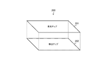
- FIG. 2 is a view showing an example of a laminated structure of the solid-state imaging device 200 according to the first embodiment of the present technology.
- the solid-state imaging device 200 includes a detection chip 202 and a light receiving chip 201 stacked on the detection chip 202. These chips are electrically connected via connections such as vias. In addition to the vias, Cu--Cu bonding or bumps can also be used.
- the light receiving chip 201 is an example of a first chip described in the claims
- the detection chip 202 is an example of a second chip described in the claims.
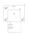
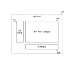
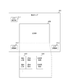
- FIG. 3 is an example of a plan view of the light receiving chip 201 in the first embodiment of the present technology.
- the light receiving chip 201 is provided with a light receiving unit 220 and via arrangement units 211, 212, and 213.
- Vias connected to the detection chip 202 are disposed in the via placement units 211, 212, and 213. Further, in the light receiving unit 220, a plurality of photodiodes 221 are arranged in a two-dimensional lattice. The photodiode 221 photoelectrically converts incident light to generate a photocurrent. Each of these photodiodes 221 is assigned a pixel address consisting of a row address and a column address, and is treated as a pixel.
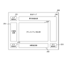
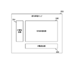
- FIG. 4 is an example of a plan view of the detection chip 202 in the first embodiment of the present technology.
- the detection chip 202 is provided with via arrangement units 231, 232 and 233, a signal processing circuit 240, a row drive circuit 251, a column drive circuit 252, and an address event detection unit 260. Vias to be connected to the light receiving chip 201 are disposed in the via placement parts 231, 232 and 233.
- the address event detection unit 260 generates a detection signal from the photocurrent of each of the plurality of photodiodes 221 and outputs the detection signal to the signal processing circuit 240.
- This detection signal is a 1-bit signal indicating whether or not the fact that the light amount of incident light has exceeded a predetermined threshold is detected as an address event.
- the row drive circuit 251 selects a row address and outputs a detection signal corresponding to the row address to the address event detection unit 260.
- the column drive circuit 252 selects a column address and outputs a detection signal corresponding to the column address to the address event detection unit 260.
- the signal processing circuit 240 performs predetermined signal processing on the detection signal from the address event detection unit 260.
- the signal processing circuit 240 arranges detection signals as pixel signals in a two-dimensional grid, and acquires image data having 1-bit information for each pixel. Then, the signal processing circuit 240 performs signal processing such as image recognition processing on the image data.
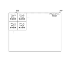
- FIG. 5 is an example of a plan view of the address event detection unit 260 according to the first embodiment of the present technology.
- a plurality of address event detection circuits 300 are arranged in a two-dimensional grid.
- a pixel address is assigned to each of the address event detection circuits 300 and connected to the photodiodes 221 of the same address.
- the address event detection circuit 300 quantizes a voltage signal corresponding to the photocurrent from the corresponding photodiode 221 and outputs it as a detection signal.
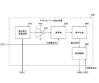
- FIG. 6 is a block diagram showing an exemplary configuration of the address event detection circuit 300 according to the first embodiment of the present technology.
- the address event detection circuit 300 includes a current-voltage conversion circuit 310, a buffer 320, a subtractor 330, a quantizer 340, and a transfer circuit 350.
- the current-voltage conversion circuit 310 converts the photocurrent from the corresponding photodiode 221 into a voltage signal.
- the current voltage conversion circuit 310 supplies a voltage signal to the buffer 320.
- the buffer 320 corrects the voltage signal from the current-voltage conversion circuit 310.
- the buffer 320 outputs the corrected voltage signal to the subtractor 330.
- Subtractor 330 reduces the level of the voltage signal from buffer 320 in accordance with the row drive signal from row drive circuit 251.
- the subtractor 330 supplies the lowered voltage signal to the quantizer 340.
- the quantizer 340 quantizes the voltage signal from the subtractor 330 into a digital signal and outputs the digital signal to the transfer circuit 350 as a detection signal.
- the transfer circuit 350 transfers the detection signal from the quantizer 340 to the signal processing circuit 240 in accordance with the column drive signal from the column drive circuit 252.
- FIG. 7 is a circuit diagram showing a configuration example of the current-voltage conversion circuit 310 according to the first embodiment of the present technology.
- the current-voltage conversion circuit 310 includes N-type transistors 311 and 313 and a P-type transistor 312. As these transistors, for example, MOS (Metal-Oxide-Semiconductor) transistors are used.
- MOS Metal-Oxide-Semiconductor
- the source of the N-type transistor 311 is connected to the cathode of the photodiode 221, and the drain is connected to the power supply terminal.
- the P-type transistor 312 and the N-type transistor 313 are connected in series between the power supply terminal and the ground terminal.
- the connection point of the P-type transistor 312 and the N-type transistor 313 is connected to the gate of the N-type transistor 311 and the input terminal of the buffer 320. Further, a predetermined bias voltage Vbias1 is applied to the gate of the P-type transistor 312.
- the drains of the N-type transistors 311 and 313 are connected to the power supply side, and such a circuit is called a source follower.
- the photocurrent from the photodiode 221 is converted into a voltage signal by the two source followers connected in a loop.
- the P-type transistor 312 supplies a constant current to the N-type transistor 313.
- ground of the light receiving chip 201 and the ground of the detection chip 202 are separated from each other to prevent interference.
- FIG. 8 is a circuit diagram showing one configuration example of the subtractor 330 and the quantizer 340 in the first embodiment of the present technology.
- Subtractor 330 includes capacitors 331 and 333, an inverter 332, and a switch 334.
- the quantizer 340 also includes a comparator 341.
- Capacitor 333 is connected in parallel to inverter 332.
- the switch 334 opens and closes a path connecting both ends of the capacitor 333 according to a row driving signal.
- the inverter 332 inverts the voltage signal input through the capacitor 331.
- the inverter 332 outputs the inverted signal to the non-inverted input terminal (+) of the comparator 341.
- Expression 5 represents the subtraction operation of the voltage signal, and the gain of the subtraction result is C1 / C2. Since it is usually desired to maximize the gain, it is preferable to design C1 large and C2 small. On the other hand, if C2 is too small, the kTC noise may increase and the noise characteristics may deteriorate, so the capacity reduction of C2 is limited to a range where noise can be tolerated.
- the address event detection circuit 300 including the subtractor 330 is mounted for each pixel, the capacitances C1 and C2 have an area limitation. Taking these into consideration, for example, C1 is set to a value of 20 to 200 femtofarads (fF), and C2 is set to a value of 1 to 20 femtofarads (fF).
- the comparator 341 compares the voltage signal from the subtractor 330 with a predetermined threshold voltage Vth applied to the inverting input terminal ( ⁇ ). The comparator 341 outputs a signal indicating the comparison result to the transfer circuit 350 as a detection signal.
- a simple pixel circuit including a photodiode and three or four transistors is disposed for each pixel.
- the pixel circuit composed of the photodiode 221 and the address event detection circuit 300 which is more complicated than the synchronous type, is Provided. Therefore, if both the photodiode 221 and the address event detection circuit 300 are disposed on the same chip, the mounting area will be larger than that of the synchronous type. Therefore, in the solid-state imaging device 200, the mounting area is reduced by distributing and arranging the photodiode 221 and the address event detection circuit 300 on the light receiving chip 201 and the detection chip 202, which are stacked.
- the photodiode 221 is disposed in the light receiving chip 201 and the address event detection circuit 300 is disposed in the detection chip 202, mounting is more than when they are disposed in the same chip. The area can be reduced.
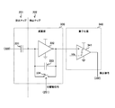
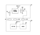
- FIG. 9 is a circuit diagram showing an example of a circuit provided in each of the light receiving chip 201 and the detection chip 202 in a modification of the first embodiment of the present technology.
- the light receiving chip 201 is further provided with N-type transistors 311 and 313 in addition to the photodiode 221.
- the detection chip 202 is provided with a P-type transistor 312 and a circuit at the subsequent stage.
- the circuit scale of the detection chip 202 can be reduced by the amount of these transistors. Further, by making the transistors in the light receiving chip 201 only N-type, the number of steps in forming the transistors can be reduced as compared with the case where N-type transistors and P-type transistors are mixed. Thereby, the manufacturing cost of the light receiving chip 201 can be reduced.
- the N-type transistors 311 and 313 are disposed in the light receiving chip 201, the manufacturing cost and the circuit size of the detection chip 202 can be reduced.
- Second embodiment> In the first embodiment described above, all of the circuits in the address event detection circuit 300 are disposed in the detection chip 202. However, as the number of pixels increases, the circuit scale of the circuits in the detection chip 202 increases. There is a risk of The solid-state imaging device 200 of the second embodiment is different from the first embodiment in that the current voltage conversion circuit 310 and the buffer 320 in the address event detection circuit 300 are provided in the light receiving chip 201.
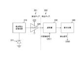
- FIG. 10 is a circuit diagram showing an example of a circuit provided in each of the light receiving chip 201 and the detection chip 202 in the second embodiment of the present technology.
- a current-voltage conversion circuit 310 and a buffer 320 are further provided in the light receiving chip 201 of the second embodiment.
- the detection chip 202 is provided with circuits after the subtractor 330.
- the circuit scale of the detection chip 202 is compared with the case where they are provided in the detection chip 202. Can be reduced.
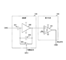
- FIG. 11 is a circuit diagram showing an example of a circuit provided in each of the light receiving chip 201 and the detection chip 202 in the first modified example of the second embodiment of the present technology.
- a capacitor 331 in the subtractor 330 is disposed.
- the capacitor 331 is an example of the first capacitor described in the claims.
- an inverter 332 in the subtractor 330, a capacitor 333 and a switch 334 are disposed.
- the inverter 332 is an example of the inverter described in the claims
- the capacitor 333 is an example of the second capacitor described in the claims.
- Capacitors such as capacitors 331 and 333 generally require a large mounting area as compared to transistors, diodes and the like. By arranging the capacitor 331 and the capacitor 333 in the light receiving chip 201 and the detection chip 202 in a distributed manner, the mounting area of the entire circuit can be reduced.
- the capacitor 331 is disposed in the light receiving chip 201 and the capacitor 333 is disposed in the detection chip 202. In comparison, the mounting area can be reduced.
- the subtractor 330 and the quantizer 340 are disposed in the detection chip 202.
- the circuit scale of the circuit in the detection chip 202 may increase.
- the solid-state imaging device 200 of the second modified example of the second embodiment differs from that of the second embodiment in that a subtractor 330 and a quantizer 340 are provided in the light receiving chip 201.
- FIG. 12 is a circuit diagram showing an example of a circuit provided in each of the light receiving chip 201 and the detection chip 202 in the second modified example of the second embodiment of the present technology.
- the light receiving chip 201 of the second modification of the second embodiment further includes a subtractor 330 and a quantizer 340 in addition to the photodiode 221, the current voltage conversion circuit 310 and the buffer 320. It differs from the second embodiment.
- the detection chip 202 is provided with a transfer circuit 350 and a signal processing circuit 240.
- the subtractor 330 and the quantizer 340 are disposed in the light receiving chip 201, so compared to the case where they are provided in the detection chip 202, The circuit scale of the detection chip 202 can be reduced.
- the current-voltage conversion circuit 310 including the N-type transistors 311 and 313 and the P-type transistor 312 is arranged in the address event detection unit 260 for each pixel.
- the circuit scale of the address event detection unit 260 may increase.
- the solid-state imaging device 200 of the third embodiment is different from that of the first embodiment in that only the N-type transistor 311 is disposed in the current-voltage conversion circuit 310.
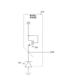
- FIG. 13 is a circuit diagram showing a configuration example of the current-voltage conversion circuit 310 according to the third embodiment of the present technology.
- the current-voltage conversion circuit 310 of the third embodiment is different from that of the first embodiment in that only the N-type transistor 311 is disposed.
- the gate and drain of the N-type transistor 311 are commonly connected to the power supply terminal, and the source is connected to the cathode of the photodiode 221.
- the connection point of the N-type transistor 311 and the photodiode 221 is connected to the input terminal of the buffer 320.
- the circuit up to the buffer 320 can be arranged in the light receiving chip 201 as in the second embodiment. Also in the third embodiment, the circuit up to the capacitor 331 can be disposed on the light receiving chip 201 as in the first modification of the second embodiment. Also in the third embodiment, the circuit up to the quantizer 340 can be disposed on the light receiving chip 201 as in the second modification of the second embodiment.
- the circuit size of the current-voltage conversion circuit 310 can be reduced compared to the case where three transistors are disposed. It can be reduced.
- the current-voltage conversion circuit 310 including the N-type transistors 311 and 313 and the P-type transistor 312 is arranged in the address event detection unit 260 for each pixel.
- the circuit scale of the address event detection unit 260 may increase.
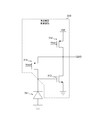
- the solid-state imaging device 200 of the fourth embodiment is different from that of the first embodiment in that only a diode is disposed in the current-voltage conversion circuit 310.
- FIG. 14 is a circuit diagram showing a configuration example of the current-voltage conversion circuit 310 according to the fourth embodiment of the present technology. Only the diode 314 is disposed in the current-voltage conversion circuit 310 of the fourth embodiment. The cathode of the diode 314 is connected to the power supply terminal, and the anode is connected to the cathode of the photodiode 221. Also, the connection point of the diode 314 and the photodiode 221 is connected to the input terminal of the buffer 320.
- the circuit up to the buffer 320 can be arranged in the light receiving chip 201 as in the second embodiment. Also in the fourth embodiment, the circuit up to the capacitor 331 can be disposed on the light receiving chip 201 as in the first modification of the second embodiment. Also in the fourth embodiment, the circuit up to the quantizer 340 can be disposed on the light receiving chip 201 as in the second modification of the second embodiment.
- the circuit scale of the current-voltage conversion circuit 310 is reduced compared to the case where three transistors are disposed. be able to.
- the current-voltage conversion circuit 310 of the fifth embodiment differs from that of the first embodiment in that a gate ground circuit is disposed to suppress low frequency noise.
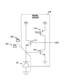
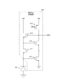
- FIG. 15 is a circuit diagram showing a configuration example of the current-voltage conversion circuit 310 according to the fifth embodiment of the present technology.
- a constant bias voltage Vbias2 is applied to the gate of the N-type transistor 311 of the fifth embodiment, the drain is connected to the cathode of the photodiode 221, and the source is the P-type transistor 312 and the N-type transistor 313. Connected to connection point.
- the gate of such an N-type transistor 311 is AC-grounded, and such a circuit is called a gate-grounded circuit.
- the arrangement of the gate ground circuit increases the closed loop gain and can suppress low frequency noise.
- the circuit up to the buffer 320 can be disposed in the light receiving chip 201 as in the second embodiment. Also in the fifth embodiment, the circuit up to the capacitor 331 can be disposed on the light receiving chip 201 as in the first modification of the second embodiment. Also in the fifth embodiment, the circuit up to the quantizer 340 can be arranged on the light receiving chip 201 as in the second modification of the second embodiment.
- the gate grounded circuit is disposed in the current-voltage conversion circuit 310, low frequency noise can be suppressed as compared with the case where the source follower circuit is disposed. .
- FIG. 16 is a circuit diagram showing a configuration example of a current-voltage conversion circuit 310 according to the sixth embodiment of the present technology.
- the current-voltage conversion circuit 310 of the sixth embodiment differs from that of the first embodiment in that N-type transistors 315 and 316 are further provided.
- these transistors for example, MOS transistors are used.
- N-type transistors 315 and 311 are connected in series between the power supply terminal and photodiode 221, and P-type transistor 312 and N-type transistors 316 and 313 are connected in series between the power supply terminal and the ground terminal. Ru.
- the gate of the N-type transistor 311 is connected to the connection point of the N-type transistors 316 and 313, and the gate of the N-type transistor 315 is connected to the connection point of the P-type transistor 312 and the N-type transistor 316.
- the gate of the N-type transistor 313 is connected to the connection point of the photodiode 221 and the N-type transistor 311, as in the first embodiment.
- the gate of N-type transistor 316 is connected to the connection point of N-type transistors 311 and 315. Also, a connection point of the P-type transistor 312 and the N-type transistor 316 is connected to the buffer 320.
- N-type transistors 315 and 311 are examples of the first N-type transistor described in the claims, and N-type transistors 316 and 313 are the second N-type transistors described in the claims. It is an example.
- the conversion gain can be increased as compared with the case of only one stage.
- the circuit in the solid-state imaging device 200 is dispersedly disposed on two chips, but the mounting area of the circuit in the solid-state imaging device 200 is increased as the number of pixels is increased. May increase.
- the solid-state imaging device 200 of the seventh embodiment is different from that of the first embodiment in that the circuits are disposed in a distributed manner on three chips.
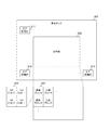
- FIG. 17 is a view showing an example of the laminated structure of the solid-state imaging device 200 according to the seventh embodiment of the present technology.
- the solid-state imaging device 200 of the seventh embodiment is different from the first embodiment in that the solid-state imaging device 200 further includes a signal processing chip 203 in addition to the light receiving chip 201 and the detection chip 202. These chips are stacked.
- FIG. 18 is an example of a plan view of a detection chip 202 according to a seventh embodiment of the present technology.
- the detection chip 202 of the seventh embodiment is different from the first embodiment in that the row drive circuit 251, the column drive circuit 252, and the signal processing circuit 240 are not disposed. Also, via placement units 253 and 254 are disposed instead of via placement units 231, 232 and 233.
- the configuration of the light receiving chip 201 of the seventh embodiment is the same as that of the first embodiment except that the via arrangement parts 211, 212 and 213 are not arranged.
- FIG. 19 is an example of a plan view of the signal processing chip 203 according to the seventh embodiment of the present technology.
- a row drive circuit 251, a column drive circuit 252, and a signal processing circuit 240 are arranged.
- the circuit in the solid-state imaging device 200 is distributed and disposed in three sheets of the light receiving chip 201, the detection chip 202, and the signal processing chip 203, they are dispersed in two.
- the mounting area can be further reduced as compared with the case of arranging them.
- the address event detection circuit 300 is arranged for each pixel in the detection chip 202 in the first embodiment described above, the circuit scale of the detection chip 202 may increase as the number of pixels increases.
- the solid-state imaging device 200 of the eighth embodiment is different from that of the first embodiment in that a plurality of pixels share one address event detection circuit 300.
- FIG. 20 is an example of a plan view of the light receiving chip 201 in the eighth embodiment of the present technology.
- the light receiving chip 201 of the eighth embodiment is different from that of the first embodiment in that a plurality of pixel blocks 222 are arranged in a two-dimensional grid in the light receiving unit 220.
- a plurality of (for example, four) photodiodes 221 are disposed in each of the pixel blocks 222.
- a pixel address is assigned to each of the photodiodes 221 and is treated as a pixel.
- FIG. 21 is an example of a plan view of the address event detection unit 260 according to the eighth embodiment of the present technology.
- the multiplexer 261 and the address event detection circuit 300 are disposed for each pixel block 222.
- the multiplexer 261 selects one of the photocurrents from the corresponding plurality of photodiodes 221 and supplies the selected one to the address event detection circuit 300.
- the control of the multiplexer 261 is performed by, for example, the row drive circuit 251.
- the address event detection circuit 300 is connected to the corresponding photodiode 221 via the multiplexer 261.
- the circuit scale per pixel is reduced compared to the case where they are not shared. be able to.
- the multiplexer 261 and the address event detection circuit 300 are arranged for each pixel in the detection chip 202, but the circuit scale of the detection chip 202 may increase as the number of pixels increases. .
- the solid-state imaging device 200 according to the modification of the eighth embodiment is different from the first embodiment in that the multiplexer 261 is disposed in the light receiving chip 201.
- FIG. 22 is an example of a plan view of the light receiving chip 201 in a modification of the eighth embodiment of the present technology.
- the light receiving chip 201 of the modification of the eighth embodiment is different from that of the eighth embodiment in that the multiplexer 261 is further disposed in the pixel block 222.
- the circuit size of the detection chip 202 is reduced compared to the case where the multiplexer 261 is provided in the detection chip 202. can do.
- the circuits are arranged in each of the light receiving chip 201 and the detection chip 202, but there is a possibility that electromagnetic noise may be generated due to the operation of these circuits.
- the solid-state imaging device 200 according to the ninth embodiment is different from the first embodiment in that a shield is provided between the light receiving chip 201 and the detection chip 202.
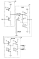
- FIG. 23 is a circuit diagram showing an example of an arrangement position of a shield in the ninth embodiment of the present technology.
- the light receiving chip 201 of the ninth embodiment is different from the first embodiment in that a current-voltage conversion circuit 310 and a buffer 320 are additionally provided in addition to the photodiode 221.
- a subtractor 330 and a quantizer 340 are disposed in the detection chip 202.
- shields 401, 402 and 403 are disposed between the light receiving chip 201 and the detection chip 202.
- the shields 401 and 402 are disposed immediately below the photodiode 221 with the light receiving chip 201 side up.
- the shield 402 is disposed immediately below the current voltage conversion circuit 310.
- the buffer 320 and the subtractor 330 are connected by a Cu-Cu connection.
- the shield 403 is disposed immediately below the buffer 320, and a signal line connecting the buffer 320 and the subtractor 330 is routed through the shield 403.
- electromagnetic shields are used as these shields 401, 402 and 403, for example, electromagnetic shields are used.
- the photodiode 221, the current-voltage conversion circuit 310, and the buffer 320 are disposed in the light receiving chip 201.
- the present invention is not limited to this configuration.
- only the photodiode 221 may be disposed on the light receiving chip 201.
- the same arrangement as that of the first modification or the second modification of the second embodiment may be employed.
- the shields 401 to 403 are disposed between the light receiving chip 201 and the detection chip 202, the generation of electromagnetic noise can be suppressed.
- the solid-state imaging device 200 captures image data composed of detection signals, but it is not possible to measure the distance to an object from the image data.
- Methods of measuring the distance include a method using stereo images and a ToF (Time of Flight) method. In these methods, it is necessary to add a camera separately from the imaging lens 110 and the solid-state imaging device 200. . Therefore, in the configuration in which the distance is determined by these methods, the number of parts and the cost may be increased.
- the solid-state imaging device 200 according to the tenth embodiment is different from that according to the first embodiment in that the distance is measured by using an image plane phase difference method with phase difference pixels.
- FIG. 24 is an example of a plan view of the light receiving chip 201 in the tenth embodiment of the present technology.
- the light receiving chip 201 of the tenth embodiment is different from the first embodiment in that a plurality of normal pixels 223 and a plurality of pairs of phase difference pixels 224 are disposed in the light receiving section 220.
- the normal pixel 223 is a pixel for generating image data.
- the phase difference pixel 224 is a pixel for obtaining the phase difference between two images.
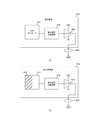
- FIG. 25 is a circuit diagram showing a configuration example of the normal pixel 223 and the phase difference pixel 224 according to the tenth embodiment of the present technology.
- a is a circuit diagram showing an example of the configuration of the normal pixel 223, and b in the figure is a circuit diagram showing an example of the configuration of the phase difference pixel 224.
- a photodiode 221, a current-voltage conversion circuit 310, and a buffer 320 are disposed. Further, the shield 403 is disposed immediately below the buffer 320. As in the ninth embodiment, the shields 401 and 402 can be further disposed.
- phase difference pixel 224 a photodiode 411, a current / voltage conversion circuit 413, and a buffer 414 are disposed.
- the configurations of the photodiode 411, the current-voltage conversion circuit 413, and the buffer 414 are similar to those of the photodiode 221, the current-voltage conversion circuit 310, and the buffer 320.
- a part of the photodiode 411 is shielded by the light shielding portion 412.
- the portions shielded by one of the pair of phase difference pixels 224 and the other are different.
- the signal processing circuit 240 obtains a phase difference from detection signals from the plurality of pairs of phase difference pixels 224, and measures a distance from the phase difference. The measured distance is used for AF (Auto Focus) and the like.
- the solid-state imaging device 200 can measure the distance to the object based on the detection signal of those pixels. it can.
- the current-voltage conversion circuit 310 is disposed for each pixel in the detection chip 202.
- the circuit size and mounting area of the detection chip 202 may increase as the number of pixels increases. is there.
- the solid-state imaging device 200 according to the eleventh embodiment is different from the first embodiment in that a plurality of pixels share one current-voltage conversion circuit 310.
- FIG. 26 is an example of a plan view of the light receiving chip 201 in the eleventh embodiment of the present technology.
- the light receiving chip 201 according to the eleventh embodiment is different from the first embodiment in that a plurality of pixel blocks 222 are arranged in a two-dimensional grid in the light receiving unit 220.
- each of the pixel blocks 222 a plurality of (two etc.) photodiodes 221, a multiplexer 261, a current / voltage conversion circuit 310, and a buffer 320 are disposed.
- the multiplexer 261 selects one of the photocurrents from each of the plurality of photodiodes 221 in the pixel block 222 and supplies it to the current-voltage conversion circuit 310.
- FIG. 27 is a circuit diagram showing an example of an arrangement position of a shield in the eleventh embodiment of the present technology.
- the shield 403 is disposed immediately below the buffer 320.
- the shields 401 and 402 can be further disposed.
- the circuit scale per pixel is reduced compared to the case where they are not shared. can do.
- the solid-state imaging device 200 compares the voltage signal with one threshold voltage to generate a 1-bit detection signal for each pixel. However, since only one bit of information is generated for each pixel, the image quality of the image data is degraded as compared to the case where a plurality of bits are generated for each pixel.
- the solid-state imaging device 200 of the twelfth embodiment is different from that of the first embodiment in that a detection signal of a plurality of bits is generated for each pixel by comparing a voltage signal with a plurality of threshold voltages.
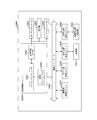
- FIG. 28 is a circuit diagram showing a configuration example of the buffer 320, the subtractor 330 and the quantizer 340 in the twelfth embodiment of the present technology.
- the buffer 320 includes N-type transistors 321 and 322.
- Subtractor 330 includes capacitors 331 and 333 and N-type transistors 335 to 337.
- the quantizer 340 includes N-type transistors 342 to 345. As transistors in these circuits, for example, MOS transistors are used.
- N-type transistors 321 and 322 are connected in series between the power supply terminal and the ground terminal. Further, a predetermined bias voltage Vbias3 is applied to the gate of the N-type transistor 321, and the gate of the N-type transistor 322 is connected to the current-voltage conversion circuit 310. The connection point of the N-type transistors 321 and 322 is connected to one end of the capacitor 331.
- N-type transistors 336 and 337 are connected in series between the power supply terminal and the ground terminal.
- a predetermined bias voltage Vbias4 is applied to the gate of the N-type transistor 337.
- the other end of the capacitor 331 is connected to the gate of the N-type transistor 336.
- One end of capacitor 333 is connected to the gate of N-type transistor 336, and the other end is input to the connection point of N-type transistors 336 and 337.
- the source and drain of the N-type transistor 335 are connected to both ends of the capacitor 333, and the row drive signal from the row drive circuit 251 is input to the gate.
- the N-type transistor 335 functions as the switch 334 illustrated in FIG.
- the N-type transistors 342 and 343 are connected in series between the power supply terminal and the ground terminal.
- N-type transistors 344 and 345 are also connected in series between the power supply terminal and the ground terminal.
- the gates of N-type transistors 342 and 344 are connected to the connection point of N-type transistors 336 and 337.
- the threshold voltage Vth1 is input to the gate of the N-type transistor 343, and the threshold voltage Vth2 lower than Vth1 is input to the gate of the N-type transistor 345.
- the connection point of N-type transistors 342 and 343 outputs a positive side (+) 1-bit detection signal
- the connection point of N-type transistors 344 and 345 outputs a negative side (-) 1-bit detection signal Is output.
- the quantizer 340 compares the voltage signal with the two threshold voltages to generate a 2-bit detection signal. For this reason, the solid-state imaging device 200 can generate image data having 2-bit information for each pixel.
- the solid-state imaging device 200 compares the voltage signal with the plurality of threshold voltages to generate a detection signal of a plurality of bits for each pixel.
- the image quality of the image data can be improved as compared to the case of generating a bit detection signal.
- the technology according to the present disclosure can be applied to various products.
- the technology according to the present disclosure is realized as a device mounted on any type of mobile object such as a car, an electric car, a hybrid electric car, a motorcycle, a bicycle, personal mobility, an airplane, a drone, a ship, a robot May be
- FIG. 29 is a block diagram showing a schematic configuration example of a vehicle control system that is an example of a mobile control system to which the technology according to the present disclosure can be applied.
- Vehicle control system 12000 includes a plurality of electronic control units connected via communication network 12001.
- the vehicle control system 12000 includes a drive system control unit 12010, a body system control unit 12020, an external information detection unit 12030, an in-vehicle information detection unit 12040, and an integrated control unit 12050.
- a microcomputer 12051, an audio image output unit 12052, and an in-vehicle network I / F (interface) 12053 are illustrated.
- the driveline control unit 12010 controls the operation of devices related to the driveline of the vehicle according to various programs.
- the drive system control unit 12010 includes a drive force generation device for generating a drive force of a vehicle such as an internal combustion engine or a drive motor, a drive force transmission mechanism for transmitting the drive force to the wheels, and a steering angle of the vehicle. It functions as a control mechanism such as a steering mechanism that adjusts and a braking device that generates a braking force of the vehicle.
- Body system control unit 12020 controls the operation of various devices equipped on the vehicle body according to various programs.
- the body system control unit 12020 functions as a keyless entry system, a smart key system, a power window device, or a control device of various lamps such as a headlamp, a back lamp, a brake lamp, a blinker or a fog lamp.
- the body system control unit 12020 may receive radio waves or signals of various switches transmitted from a portable device substituting a key.
- Body system control unit 12020 receives the input of these radio waves or signals, and controls a door lock device, a power window device, a lamp and the like of the vehicle.
- Outside vehicle information detection unit 12030 detects information outside the vehicle equipped with vehicle control system 12000.
- an imaging unit 12031 is connected to the external information detection unit 12030.
- the out-of-vehicle information detection unit 12030 causes the imaging unit 12031 to capture an image outside the vehicle, and receives the captured image.
- the external information detection unit 12030 may perform object detection processing or distance detection processing of a person, a vehicle, an obstacle, a sign, characters on a road surface, or the like based on the received image.
- the imaging unit 12031 is an optical sensor that receives light and outputs an electrical signal according to the amount of light received.
- the imaging unit 12031 can output an electric signal as an image or can output it as distance measurement information.
- the light received by the imaging unit 12031 may be visible light or non-visible light such as infrared light.
- In-vehicle information detection unit 12040 detects in-vehicle information.
- a driver state detection unit 12041 that detects a state of a driver is connected to the in-vehicle information detection unit 12040.
- the driver state detection unit 12041 includes, for example, a camera for imaging the driver, and the in-vehicle information detection unit 12040 determines the degree of fatigue or concentration of the driver based on the detection information input from the driver state detection unit 12041. It may be calculated or it may be determined whether the driver does not go to sleep.
- the microcomputer 12051 calculates a control target value of the driving force generation device, the steering mechanism or the braking device based on the information inside and outside the vehicle acquired by the outside information detecting unit 12030 or the in-vehicle information detecting unit 12040, and a drive system control unit A control command can be output to 12010.
- the microcomputer 12051 controls the driving force generating device, the steering mechanism, the braking device, and the like based on the information around the vehicle acquired by the outside information detecting unit 12030 or the in-vehicle information detecting unit 12040 so that the driver can Coordinated control can be performed for the purpose of automatic driving that travels autonomously without depending on the operation.
- the microcomputer 12051 can output a control command to the body system control unit 12020 based on the information outside the vehicle acquired by the external information detection unit 12030.
- the microcomputer 12051 controls the headlamp according to the position of the preceding vehicle or oncoming vehicle detected by the external information detection unit 12030, and performs cooperative control for the purpose of antiglare such as switching the high beam to the low beam. It can be carried out.
- the audio image output unit 12052 transmits an output signal of at least one of audio and image to an output device capable of visually or aurally notifying information to a passenger or the outside of a vehicle.
- an audio speaker 12061, a display unit 12062, and an instrument panel 12063 are illustrated as output devices.
- the display unit 12062 may include, for example, at least one of an on-board display and a head-up display.
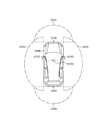
- FIG. 30 is a diagram illustrating an example of the installation position of the imaging unit 12031.
- imaging units 12101, 12102, 12103, 12104, and 12105 are included.
- the imaging units 12101, 12102, 12103, 12104, and 12105 are provided, for example, at positions such as the front nose of the vehicle 12100, a side mirror, a rear bumper, a back door, and an upper portion of a windshield of a vehicle interior.
- the imaging unit 12101 provided in the front nose and the imaging unit 12105 provided in the upper part of the windshield in the vehicle cabin mainly acquire an image in front of the vehicle 12100.
- the imaging units 12102 and 12103 included in the side mirror mainly acquire an image of the side of the vehicle 12100.
- the imaging unit 12104 provided in the rear bumper or the back door mainly acquires an image of the rear of the vehicle 12100.
- the imaging unit 12105 provided on the top of the windshield in the passenger compartment is mainly used to detect a leading vehicle or a pedestrian, an obstacle, a traffic light, a traffic sign, a lane, or the like.
- FIG. 30 shows an example of the imaging range of the imaging units 12101 to 12104.
- the imaging range 12111 indicates the imaging range of the imaging unit 12101 provided on the front nose
- the imaging ranges 12112 and 12113 indicate the imaging ranges of the imaging units 12102 and 12103 provided on the side mirrors
- the imaging range 12114 indicates The imaging range of the imaging part 12104 provided in the rear bumper or the back door is shown. For example, by overlaying the image data captured by the imaging units 12101 to 12104, a bird's eye view of the vehicle 12100 viewed from above can be obtained.
- At least one of the imaging units 12101 to 12104 may have a function of acquiring distance information.
- at least one of the imaging units 12101 to 12104 may be a stereo camera including a plurality of imaging devices, or an imaging device having pixels for phase difference detection.
- the microcomputer 12051 measures the distance to each three-dimensional object in the imaging ranges 12111 to 12114, and the temporal change of this distance (relative velocity with respect to the vehicle 12100). In particular, it is possible to extract a three-dimensional object traveling at a predetermined speed (for example, 0 km / h or more) in substantially the same direction as the vehicle 12100 as a leading vehicle, in particular by finding the it can. Further, the microcomputer 12051 can set an inter-vehicle distance to be secured in advance before the preceding vehicle, and can perform automatic brake control (including follow-up stop control), automatic acceleration control (including follow-up start control), and the like. As described above, it is possible to perform coordinated control for the purpose of automatic driving or the like that travels autonomously without depending on the driver's operation.
- automatic brake control including follow-up stop control
- automatic acceleration control including follow-up start control
- the microcomputer 12051 converts three-dimensional object data relating to a three-dimensional object into a two-wheeled vehicle, an ordinary vehicle, a large vehicle, a pedestrian, a telephone pole, or other three-dimensional object It can be classified, extracted and used for automatic avoidance of obstacles. For example, the microcomputer 12051 identifies obstacles around the vehicle 12100 into obstacles visible to the driver of the vehicle 12100 and obstacles difficult to see.
- the microcomputer 12051 determines the collision risk indicating the degree of risk of collision with each obstacle, and when the collision risk is a setting value or more and there is a possibility of a collision, through the audio speaker 12061 or the display unit 12062 By outputting a warning to the driver or performing forcible deceleration or avoidance steering via the drive system control unit 12010, driving support for collision avoidance can be performed.
- At least one of the imaging units 12101 to 12104 may be an infrared camera that detects infrared light.
- the microcomputer 12051 can recognize a pedestrian by determining whether a pedestrian is present in the images captured by the imaging units 12101 to 12104.
- pedestrian recognition is, for example, a procedure for extracting feature points in images captured by the imaging units 12101 to 12104 as an infrared camera, and pattern matching processing on a series of feature points indicating the outline of an object to determine whether it is a pedestrian or not
- the procedure is to determine
- the audio image output unit 12052 generates a square outline for highlighting the recognized pedestrian.
- the display unit 12062 is controlled so as to display a superimposed image. Further, the audio image output unit 12052 may control the display unit 12062 to display an icon or the like indicating a pedestrian at a desired position.
- the example of the vehicle control system to which the technology according to the present disclosure can be applied has been described above.
- the technology according to the present disclosure may be applied to, for example, the imaging unit 12031 among the configurations described above.
- the imaging device 100 of FIG. 1 can be applied to the imaging unit 12031 of FIG.
- the mounting area of the circuit can be reduced and the imaging unit 12031 can be miniaturized.
- the present technology can also be configured as follows.
- the row drive circuit and the column drive circuit are provided on a second chip,
- the photodiode is provided on a first chip, At least a part of the pixel circuit is provided in the second chip, and is a solid-state imaging device electrically connected to the photodiode provided in the first chip through the connection portion.
- the first chip is further provided with a plurality of N-type transistors that convert the photocurrent into the voltage signal and output it.
- the second chip further includes a current-voltage conversion circuit that converts the photocurrent to the voltage signal.
- the current-voltage conversion circuit A drain connected to a cathode of the photodiode, and an N-type transistor having a gate and a source commonly connected to a power supply, The connection point between the N-type transistor and the photodiode is connected to the input terminal of the buffer (3).
- the current-voltage conversion circuit A first N-type transistor with a predetermined bias voltage applied to its gate and a drain connected to the cathode of the photodiode; And a second N-type transistor having a gate connected to a connection point between the photodiode and the first transistor, a drain connected to a source of the first N-type transistor, and a source connected to ground.
- the connection point of the said 1st and 2nd transistor is a solid-state image sensor in any one of said (3) to (5) connected to the input terminal of the said buffer.
- the current-voltage conversion circuit includes a plurality of stages of loop circuits, Each of the plurality of stages of loop circuits is A first N-type transistor, The second N-type transistor having a gate connected to the source of the first N-type transistor and a drain connected to the gate of the first N-type transistor.
- the solid-state imaging device according to claim 1.
- the first chip is further provided with a current-voltage conversion circuit that converts the photocurrent to the voltage signal and a buffer that corrects and outputs the voltage signal (1)
- the solid-state image sensor of description The solid-state image sensor of description.
- the first chip is further provided with a first capacitor whose one end is connected to the output terminal of the buffer,
- a subtractor that lowers the level of the voltage signal output from the buffer and a quantizer that quantizes the lowered voltage signal and outputs it as the detection signal in the first chip
- the solid-state imaging device further comprising: (1) A light receiving chip provided with a photodiode that photoelectrically converts incident light to generate a photocurrent; A solid-state image pickup device comprising: a detection chip which quantizes a voltage signal corresponding to the photocurrent and outputs it as a detection signal.
- the light receiving chip is further provided with a plurality of N-type transistors that convert the photocurrent into the voltage signal and output the voltage signal.
- the solid-state imaging device wherein the detection chip is further provided with a P-type transistor for supplying a constant current to any one of the plurality of N-type transistors.
- the detection chip is further provided with a current-voltage conversion circuit that converts the photocurrent into the voltage signal.
- the current-voltage conversion circuit A drain connected to a cathode of the photodiode, and an N-type transistor having a gate and a source commonly connected to a power supply, The connection point between the N-type transistor and the photodiode is connected to the input terminal of the buffer (3).
- the current-voltage conversion circuit An anode connected to a cathode of the photodiode, the cathode including a diode connected to a power supply, The connection point of the said diode and the said photodiode is a solid-state image sensor as described in said (3) or (4) connected to the input terminal of the said buffer.
- the current-voltage conversion circuit A first N-type transistor with a predetermined bias voltage applied to its gate and a drain connected to the cathode of the photodiode; And a second N-type transistor having a gate connected to a connection point between the photodiode and the first transistor, a drain connected to a source of the first N-type transistor, and a source connected to ground.
- the connection point of the said 1st and 2nd transistor is a solid-state image sensor in any one of said (3) to (5) connected to the input terminal of the said buffer.
- the current-voltage conversion circuit includes a plurality of stages of loop circuits, Each of the plurality of stages of loop circuits is A first N-type transistor, The second N-type transistor having a gate connected to the source of the first N-type transistor and a drain connected to the gate of the first N-type transistor.
- the light receiving chip is further provided with a first capacitor whose one end is connected to the output terminal of the buffer,
- the light receiving chip is further provided with a subtractor for reducing the level of the voltage signal output from the buffer, and a quantizer for quantizing the reduced voltage signal and outputting the result as the detection signal.
- (11) The solid-state imaging device according to any one of (1) to (10), further including a signal processing chip that processes the detection signal.
- the light receiving chip is provided with a light receiving portion in which a predetermined number of the photodiodes are arranged in a two-dimensional grid shape
- the detection chip is provided with an address event detection circuit that outputs the detection signal
- the detection chip is further provided with a multiplexer that selects one of the photocurrents of the plurality of photodiodes and outputs the selected photocurrent to the address event detection circuit.
- the solid-state imaging device (14) The solid-state imaging device according to (12), wherein the light receiving chip is further provided with a multiplexer that selects one of the photocurrents of the plurality of photodiodes and outputs the selected photocurrent to the address event detection circuit.
- the solid-state imaging device according to any one of (1) to (14), further including a shield provided between the light receiving chip and the detection chip.
- the photodiode is provided in each of the normal pixel and the phase difference pixel, The solid-state imaging device according to any one of (1) to (15), wherein a part of the photodiode of the phase difference pixel is shielded from light.
- the light receiving chip is provided with a predetermined number of the photodiodes arranged in a two-dimensional grid and a current-voltage conversion circuit that converts the photocurrent into the voltage signal.
- the solid-state imaging device according to (1) wherein a plurality of adjacent photodiodes among the predetermined number of the photodiodes are commonly connected to the current-voltage conversion circuit.
- the detection chip is provided with a quantizer which compares the voltage signal with a plurality of threshold voltages and outputs a signal of a plurality of bits indicating the comparison result as the detection signal.
- imaging device 110 imaging lens 120 recording unit 130 control unit 200 solid-state imaging device 201 light receiving chip 202 detection chip 203 signal processing chip 211, 212, 213, 231, 232, 233, 253, 254 via arrangement unit 220 light receiving unit 221, 411 Photodiode 222 Pixel block 223 Normal pixel 224 Phase difference pixel 240 Signal processing circuit 251 Row drive circuit 252 Column drive circuit 260 Address event detection unit 261 Multiplexer 300 Address event detection circuit 310, 413 Current voltage conversion circuit 311, 313, 315, 316 , 321, 322, 335 to 337, 342 to 345 N type transistor 312 P type transistor 314 diode 320, 332, 414 buffer 330 subtractor 331, 333 Capacitor 334 switch 340 quantizer 341 comparator 350 transfer circuit 401, 402, 403 shield 412 light-shielding portion 12031 imaging unit
Landscapes
- Engineering & Computer Science (AREA)
- Multimedia (AREA)
- Signal Processing (AREA)
- Solid State Image Pick-Up Elements (AREA)
- Transforming Light Signals Into Electric Signals (AREA)
Abstract
Description
1.第1の実施の形態(受光チップにフォトダイオードを配置する例)
2.第2の実施の形態(受光チップにフォトダイオード、電流電圧変換回路およびバッファを配置する例)
3.第3の実施の形態(受光チップにフォトダイオードを配置し、電流電圧変換回路内にN型トランジスタ1つを配置する例)
4.第4の実施の形態(受光チップにフォトダイオードを配置し、電流電圧変換回路内にダイオードを配置する例)
5.第5の実施の形態(受光チップにフォトダイオードを配置し、電流電圧変換回路内にゲート接地回路を配置する例)
6.第6の実施の形態(受光チップにフォトダイオードを配置し、電流電圧変換回路内に2段のループ回路を配置する例)
7.第7の実施の形態(受光チップにフォトダイオードを配置し、残りを検出チップおよび信号処理チップに配置する例)
8.第8の実施の形態(受光チップにフォトダイオードを配置し、複数の画素でアドレスイベント検出回路を共有する例)
9.第9の実施の形態(受光チップにフォトダイオードを配置し、検出チップとの間にシールドを配置する例)
10.第10の実施の形態(受光チップ内の通常画素および位相差画素のそれぞれにフォトダイオードを配置する例)
11.第11の実施の形態(受光チップにフォトダイオードを配置し、複数の画素で電流電圧変換回路を共有する例)
12.第12の実施の形態(受光チップにフォトダイオードを配置し、電圧信号を複数の閾値電圧と比較する例)
13.移動体への応用例
[撮像装置の構成例]
図1は、本技術の第1の実施の形態における撮像装置100の一構成例を示すブロック図である。この撮像装置100は、撮像レンズ110、固体撮像素子200、記録部120および制御部130を備える。撮像装置100としては、産業用ロボットに搭載されるカメラや、車載カメラなどが想定される。
図2は、本技術の第1の実施の形態における固体撮像素子200の積層構造の一例を示す図である。この固体撮像素子200は、検出チップ202と、その検出チップ202に積層された受光チップ201とを備える。これらのチップは、ビアなどの接続部を介して電気的に接続される。なお、ビアの他、Cu-Cu接合やバンプにより接続することもできる。なお、受光チップ201は、特許請求の範囲に記載の第1のチップの一例であり、検出チップ202は、特許請求の範囲に記載の第2のチップの一例である。
図6は、本技術の第1の実施の形態におけるアドレスイベント検出回路300の一構成例を示すブロック図である。このアドレスイベント検出回路300は、電流電圧変換回路310、バッファ320、減算器330、量子化器340および転送回路350を備える。
図7は、本技術の第1の実施の形態における電流電圧変換回路310の一構成例を示す回路図である。この電流電圧変換回路310は、N型トランジスタ311および313とP型トランジスタ312とを備える。これらのトランジスタとして、例えば、MOS(Metal-Oxide-Semiconductor)トランジスタが用いられる。
図8は、本技術の第1の実施の形態における減算器330および量子化器340の一構成例を示す回路図である。減算器330は、コンデンサ331および333と、インバータ332と、スイッチ334とを備える。また、量子化器340は、コンパレータ341を備える。
Qinit=C1×Vinit ・・・式1
一方、コンデンサ333に蓄積される電荷Q2は、出力電圧をVoutとすると、次の式により表される。
Q2=-C2×Vout ・・・式3
Qinit=Qafter+Q2 ・・・式4
Vout=-(C1/C2)×(Vafter-Vinit) ・・・式5
上述の第1の実施の形態では、電流電圧変換回路310の全てを検出チップ202に配置していたが、画素数の増大に伴って、検出チップ202内の回路の回路規模が増大するおそれがある。この第1の実施の形態の変形例の固体撮像素子200は、電流電圧変換回路310の一部の回路を受光チップ201に設けた点において第1の実施の形態と異なる。
上述の第1の実施の形態では、アドレスイベント検出回路300内の回路の全てを検出チップ202に配置していたが、画素数の増大に伴って、検出チップ202内の回路の回路規模が増大するおそれがある。この第2の実施の形態の固体撮像素子200は、アドレスイベント検出回路300内の電流電圧変換回路310およびバッファ320を受光チップ201に設けた点において第1の実施の形態と異なる。
上述の第2の実施の形態では、減算器330の全てを検出チップ202に配置していたが、画素数の増大に伴って、検出チップ202内の回路の回路規模や実装面積が増大するおそれがある。この第2の実施の形態の第1の変形例の固体撮像素子200は、減算器330の一部を受光チップ201に設けた点において第2の実施の形態と異なる。
上述の第2の実施の形態では、減算器330および量子化器340を検出チップ202に配置していたが、画素数の増大に伴って、検出チップ202内の回路の回路規模が増大するおそれがある。この第2の実施の形態の第2の変形例の固体撮像素子200は、減算器330および量子化器340を受光チップ201に設けた点において第2の実施の形態と異なる。
上述の第1の実施の形態では、N型トランジスタ311および313とP型トランジスタ312とからなる電流電圧変換回路310をアドレスイベント検出部260内に画素毎に配列していた。しかしながら、画素数の増大に伴って、アドレスイベント検出部260の回路規模が増大するおそれがある。この第3の実施の形態の固体撮像素子200は、N型トランジスタ311のみを電流電圧変換回路310に配置した点において第1の実施の形態と異なる。
上述の第1の実施の形態では、N型トランジスタ311および313とP型トランジスタ312とからなる電流電圧変換回路310をアドレスイベント検出部260内に画素毎に配列していた。しかしながら、画素数の増大に伴って、アドレスイベント検出部260の回路規模が増大するおそれがある。この第4の実施の形態の固体撮像素子200は、ダイオードのみを電流電圧変換回路310に配置した点において第1の実施の形態と異なる。
上述の第1の実施の形態では、ソースフォロワ回路を電流電圧変換回路310に設けていたが、一般にソースフォロワ回路は、周波数特性があまり良くない。このため、低周波ノイズが発生する際に、そのノイズを十分に抑制することができないおそれがある。この第5の実施の形態の電流電圧変換回路310は、ゲート接地回路を配置して低周波数ノイズを抑制する点において第1の実施の形態と異なる。
上述の第1の実施の形態では、1個のループ回路を電流電圧変換回路310に設けていたが、ループ回路1個のみでは、電流を電圧に変換する際の変換ゲインが不足するおそれがある。この第6の実施の形態の電流電圧変換回路310は、2段のループ回路を電流電圧変換回路310に設けた点において第1の実施の形態と異なる。
上述の第1の実施の形態では、固体撮像素子200内の回路を2枚のチップに分散して配置していたが、画素数の増大に伴って、固体撮像素子200内の回路の実装面積が増大するおそれがある。この第7の実施の形態の固体撮像素子200は、回路を3枚のチップに分散して配置した点において第1の実施の形態と異なる。
上述の第1の実施の形態では、検出チップ202においてアドレスイベント検出回路300を画素毎に配置していたが、画素数の増大に伴って検出チップ202の回路規模が増大するおそれがある。この第8の実施の形態の固体撮像素子200は、複数の画素が1つのアドレスイベント検出回路300を共有する点において第1の実施の形態と異なる。
上述の第8の実施の形態では、検出チップ202においてマルチプレクサ261およびアドレスイベント検出回路300を画素毎に配置していたが画素数の増大に伴って検出チップ202の回路規模が増大するおそれがある。この第8の実施の形態の変形例の固体撮像素子200は、マルチプレクサ261を受光チップ201に配置する点において第1の実施の形態と異なる。
上述の第1の実施の形態では、受光チップ201および検出チップ202のそれぞれに回路を配置していたが、それらの回路の動作により電磁ノイズが発生するおそれがある。この第9の実施の形態の固体撮像素子200は、受光チップ201と検出チップ202との間にシールドを設けた点において第1の実施の形態と異なる。
上述の第1の実施の形態では、固体撮像素子200は、検出信号からなる画像データを撮像していたが、この画像データから物体までの距離を測定することはできない。距離を測定する方式としては、ステレオ画像を用いる方式やToF(Time of Flight)方式などがあるが、これらの方式では撮像レンズ110や固体撮像素子200とは別途に、カメラを追加する必要がある。このため、これらの方式により距離を求める構成では、部品点数やコストが増大するおそれがある。この第10の実施の形態の固体撮像素子200は、位相差画素により、像面位相差方式を用いて距離を測定する点において第1の実施の形態と異なる。
上述の第1の実施の形態では、検出チップ202において電流電圧変換回路310を画素毎に配置していたが、画素数の増大に伴って検出チップ202の回路規模や実装面積が増大するおそれがある。この第11の実施の形態の固体撮像素子200は、複数の画素が1つの電流電圧変換回路310を共有する点において第1の実施の形態と異なる。
上述の第1の実施の形態では、固体撮像素子200は、電圧信号と1つの閾値電圧とを比較して1ビットの検出信号を画素毎に生成していた。しかし、画素毎に1ビットの情報しか生成されないため、画素毎に複数ビットを生成する場合と比較して画像データの画質が低下してしまう。この第12の実施の形態の固体撮像素子200は、電圧信号と複数の閾値電圧とを比較して複数ビットの検出信号を画素毎に生成する点において第1の実施の形態と異なる。
本開示に係る技術(本技術)は、様々な製品へ応用することができる。例えば、本開示に係る技術は、自動車、電気自動車、ハイブリッド電気自動車、自動二輪車、自転車、パーソナルモビリティ、飛行機、ドローン、船舶、ロボット等のいずれかの種類の移動体に搭載される装置として実現されてもよい。
(1)行駆動回路と、
列駆動回路と、
複数の画素とを備え、
前記複数の画素はそれぞれ、
入射光を光電変換して光電流を生成するフォトダイオードと、
前記光電流に応じた電圧信号を量子化して検出信号として出力する画素回路と、
接続部とを有し、
前記行駆動回路および前記列駆動回路は第2のチップに設けられ、
前記フォトダイオードは第1のチップに設けられ、
少なくとも一部の前記画素回路は前記第2のチップに設けられ、前記接続部を介して前記第1のチップに設けられた前記フォトダイオードに電気的に接続される固体撮像素子。
(2)前記画素回路において、
前記第1のチップには、前記光電流を前記電圧信号に変換して出力する複数のN型トランジスタがさらに設けられ、
前記第2のチップには、前記複数のN型トランジスタのいずれかに一定の電流を供給するP型トランジスタがさらに設けられる
前記(1)記載の固体撮像素子。
(3)前記画素回路において、前記第2のチップには、前記光電流を前記電圧信号に変換する電流電圧変換回路がさらに設けられる
前記(1)に記載の固体撮像素子。
(4)前記電流電圧変換回路は、
前記フォトダイオードのカソードにドレインが接続され、ゲートおよびソースが電源に共通に接続されたN型トランジスタを含み、
前記N型トランジスタと前記フォトダイオードとの接続点は、前記バッファの入力端子に接続される
前記(3)記載の固体撮像素子。
(5)前記電流電圧変換回路は、
前記フォトダイオードのカソードにアノードが接続され、カソードが電源に接続されたダイオードを含み、
前記ダイオードと前記フォトダイオードとの接続点は、前記バッファの入力端子に接続される
前記(3)または(4)に記載の固体撮像素子。
(6)前記電流電圧変換回路は、
所定のバイアス電圧がゲートに印加され、ドレインが前記フォトダイオードのカソードに接続された第1のN型トランジスタと、
前記フォトダイオードと前記第1トランジスタとの接続点にゲートが接続され、ドレインが前記第1のN型トランジスタのソースに接続され、ソースが接地された第2のN型トランジスタと
を含み、
前記第1および第2のトランジスタの接続点は、前記バッファの入力端子に接続される
前記(3)から(5)のいずれかに記載の固体撮像素子。
(7)前記電流電圧変換回路は、複数段のループ回路を含み、
前記複数段のループ回路のそれぞれは、
第1のN型トランジスタと、
前記第1のN型トランジスタのソースにゲートが接続され、前記第1のN型トランジスタのゲートにドレインが接続された第2のN型トランジスタと
を備える前記(3)から(6)のいずれかに記載の固体撮像素子。
(8)前記画素回路において、前記第1のチップには、前記光電流を前記電圧信号に変換する電流電圧変換回路と前記電圧信号を補正して出力するバッファとがさらに設けられる
前記(1)記載の固体撮像素子。
(9)前記画素回路において、
前記第1のチップには、前記バッファの出力端子に一端が接続された第1コンデンサがさらに設けられ、
前記第2のチップには、前記第1コンデンサの他端に入力端子が接続されたインバータと前記インバータに並列に接続された第2コンデンサとがさらに設けられる
前記(8)記載の固体撮像素子。
(10)前記画素回路において、前記第1のチップには、前記バッファから出力された前記電圧信号のレベルを低下させる減算器と前記低下した電圧信号を量子化して前記検出信号として出力する量子化器とがさらに設けられる
前記(8)記載の固体撮像素子。
(1)入射光を光電変換して光電流を生成するフォトダイオードが設けられた受光チップと、
前記光電流に応じた電圧信号を量子化して検出信号として出力する検出チップと
を具備する固体撮像素子。
(2)前記受光チップには、前記光電流を前記電圧信号に変換して出力する複数のN型トランジスタがさらに設けられ、
前記検出チップには、前記複数のN型トランジスタのいずれかに一定の電流を供給するP型トランジスタがさらに設けられる
前記(1)記載の固体撮像素子。
(3)前記検出チップには、前記光電流を前記電圧信号に変換する電流電圧変換回路がさらに設けられる
前記(1)記載の固体撮像素子。
(4)前記電流電圧変換回路は、
前記フォトダイオードのカソードにドレインが接続され、ゲートおよびソースが電源に共通に接続されたN型トランジスタを含み、
前記N型トランジスタと前記フォトダイオードとの接続点は、前記バッファの入力端子に接続される
前記(3)記載の固体撮像素子。
(5)前記電流電圧変換回路は、
前記フォトダイオードのカソードにアノードが接続され、カソードが電源に接続されたダイオードを含み、
前記ダイオードと前記フォトダイオードとの接続点は、前記バッファの入力端子に接続される
前記(3)または(4)に記載の固体撮像素子。
(6)前記電流電圧変換回路は、
所定のバイアス電圧がゲートに印加され、ドレインが前記フォトダイオードのカソードに接続された第1のN型トランジスタと、
前記フォトダイオードと前記第1トランジスタとの接続点にゲートが接続され、ドレインが前記第1のN型トランジスタのソースに接続され、ソースが接地された第2のN型トランジスタと
を含み、
前記第1および第2のトランジスタの接続点は、前記バッファの入力端子に接続される
前記(3)から(5)のいずれかに記載の固体撮像素子。
(7)前記電流電圧変換回路は、複数段のループ回路を含み、
前記複数段のループ回路のそれぞれは、
第1のN型トランジスタと、
前記第1のN型トランジスタのソースにゲートが接続され、前記第1のN型トランジスタのゲートにドレインが接続された第2のN型トランジスタと
を備える前記(3)から(6)のいずれかに記載の固体撮像素子。
(8)前記受光チップには、前記光電流を前記電圧信号に変換する電流電圧変換回路と前記電圧信号を補正して出力するバッファとがさらに設けられる
前記(1)記載の固体撮像素子。
(9)前記受光チップには、前記バッファの出力端子に一端が接続された第1コンデンサがさらに設けられ、
前記検出チップには、前記第1コンデンサの他端に入力端子が接続されたインバータと前記インバータに並列に接続された第2コンデンサとがさらに設けられる
前記(8)記載の固体撮像素子。
(10)前記受光チップには、前記バッファから出力された前記電圧信号のレベルを低下させる減算器と前記低下した電圧信号を量子化して前記検出信号として出力する量子化器とがさらに設けられる
前記(8)記載の固体撮像素子。
(11)前記検出信号を処理する信号処理チップをさらに具備する
前記(1)から(10)のいずれかに記載の固体撮像素子。
(12)前記受光チップには、所定数の前記フォトダイオードが二次元格子状に配列された受光部が設けられ、
前記検出チップには、前記検出信号を出力するアドレスイベント検出回路が設けられ、
前記アドレスイベント検出回路は、前記受光部内で隣接する複数のフォトダイオードに共通に接続される
前記(1)記載の固体撮像素子。
(13)前記検出チップには、前記複数のフォトダイオードのそれぞれの光電流のいずれかを選択して前記アドレスイベント検出回路に出力するマルチプレクサがさらに設けられる
前記(12)記載の固体撮像素子。
(14)前記受光チップには、前記複数のフォトダイオードのそれぞれの光電流のいずれかを選択して前記アドレスイベント検出回路に出力するマルチプレクサがさらに設けられる
前記(12)記載の固体撮像素子。
(15)前記受光チップと前記検出チップとの間に設けられたシールドをさらに具備する
前記(1)から(14)のいずれかに記載の固体撮像素子。
(16)前記フォトダイオードは、通常画素と位相差画素とのそれぞれに設けられ、
前記位相差画素のフォトダイオードの一部は遮光されている
前記(1)から(15)のいずれかに記載の固体撮像素子。
(17)前記受光チップには、二次元格子状に配列された所定数の前記フォトダイオードと前記光電流を前記電圧信号に変換する電流電圧変換回路とが設けられ、
前記所定数の前記フォトダイオードのうち隣接する複数のフォトダイオードは、前記電流電圧変換回路に共通に接続される
前記(1)記載の固体撮像素子。
(18)前記検出チップには、前記電圧信号と複数の閾値電圧とを比較して当該比較結果を示す複数ビットの信号を前記検出信号として出力する量子化器が設けられる
前記(1)記載の固体撮像素子。
110 撮像レンズ
120 記録部
130 制御部
200 固体撮像素子
201 受光チップ
202 検出チップ
203 信号処理チップ
211、212、213、231、232、233、253、254 ビア配置部
220 受光部
221、411 フォトダイオード
222 画素ブロック
223 通常画素
224 位相差画素
240 信号処理回路
251 行駆動回路
252 列駆動回路
260 アドレスイベント検出部
261 マルチプレクサ
300 アドレスイベント検出回路
310、413 電流電圧変換回路
311、313、315、316、321、322、335~337、342~345 N型トランジスタ
312 P型トランジスタ
314 ダイオード
320、332、414 バッファ
330 減算器
331、333 コンデンサ
334 スイッチ
340 量子化器
341 コンパレータ
350 転送回路
401、402、403 シールド
412 遮光部
12031 撮像部
Claims (28)
- 行駆動回路と、
列駆動回路と、
複数の画素とを備え、
前記複数の画素はそれぞれ、
入射光を光電変換して光電流を生成するフォトダイオードと、
前記光電流に応じた電圧信号を量子化して検出信号として出力する画素回路と、
接続部とを有し、
前記行駆動回路および前記列駆動回路は第2のチップに設けられ、
前記フォトダイオードは第1のチップに設けられ、
少なくとも一部の前記画素回路は前記第2のチップに設けられ、前記接続部を介して前記第1のチップに設けられた前記フォトダイオードに電気的に接続される固体撮像素子。 - 前記画素回路において、
前記第1のチップには、前記光電流を前記電圧信号に変換して出力する複数のN型トランジスタがさらに設けられ、
前記第2のチップには、前記複数のN型トランジスタのいずれかに一定の電流を供給するP型トランジスタがさらに設けられる
請求項1記載の固体撮像素子。 - 前記画素回路において、前記第2のチップには、前記光電流を前記電圧信号に変換する電流電圧変換回路がさらに設けられる
請求項1記載の固体撮像素子。 - 前記電流電圧変換回路は、
前記フォトダイオードのカソードにドレインが接続され、ゲートおよびソースが電源に共通に接続されたN型トランジスタを含み、
前記N型トランジスタと前記フォトダイオードとの接続点は、前記バッファの入力端子に接続される
請求項3記載の固体撮像素子。 - 前記電流電圧変換回路は、
前記フォトダイオードのカソードにアノードが接続され、カソードが電源に接続されたダイオードを含み、
前記ダイオードと前記フォトダイオードとの接続点は、前記バッファの入力端子に接続される
請求項3記載の固体撮像素子。 - 前記電流電圧変換回路は、
所定のバイアス電圧がゲートに印加され、ドレインが前記フォトダイオードのカソードに接続された第1のN型トランジスタと、
前記フォトダイオードと前記第1トランジスタとの接続点にゲートが接続され、ドレインが前記第1のN型トランジスタのソースに接続され、ソースが接地された第2のN型トランジスタと
を含み、
前記第1および第2のトランジスタの接続点は、前記バッファの入力端子に接続される
請求項3記載の固体撮像素子。 - 前記電流電圧変換回路は、複数段のループ回路を含み、
前記複数段のループ回路のそれぞれは、
第1のN型トランジスタと、
前記第1のN型トランジスタのソースにゲートが接続され、前記第1のN型トランジスタのゲートにドレインが接続された第2のN型トランジスタと
を備える請求項3記載の固体撮像素子。 - 前記画素回路において、前記第1のチップには、前記光電流を前記電圧信号に変換する電流電圧変換回路と前記電圧信号を補正して出力するバッファとがさらに設けられる
請求項1記載の固体撮像素子。 - 前記画素回路において、
前記第1のチップには、前記バッファの出力端子に一端が接続された第1コンデンサがさらに設けられ、
前記第2のチップには、前記第1コンデンサの他端に入力端子が接続されたインバータと前記インバータに並列に接続された第2コンデンサとがさらに設けられる
請求項8記載の固体撮像素子。 - 前記画素回路において、前記第1のチップには、前記バッファから出力された前記電圧信号のレベルを低下させる減算器と前記低下した電圧信号を量子化して前記検出信号として出力する量子化器とがさらに設けられる
請求項8記載の固体撮像素子。 - 入射光を光電変換して光電流を生成するフォトダイオードが設けられた受光チップと、
前記光電流に応じた電圧信号を量子化して検出信号として出力する検出チップと
を具備する固体撮像素子。 - 前記受光チップには、前記光電流を前記電圧信号に変換して出力する複数のN型トランジスタがさらに設けられ、
前記検出チップには、前記複数のN型トランジスタのいずれかに一定の電流を供給するP型トランジスタがさらに設けられる
請求項10記載の固体撮像素子。 - 前記検出チップには、前記光電流を前記電圧信号に変換する電流電圧変換回路がさらに設けられる
請求項10記載の固体撮像素子。 - 前記電流電圧変換回路は、
前記フォトダイオードのカソードにドレインが接続され、ゲートおよびソースが電源に共通に接続されたN型トランジスタを含み、
前記N型トランジスタと前記フォトダイオードとの接続点は、前記バッファの入力端子に接続される
請求項13記載の固体撮像素子。 - 前記電流電圧変換回路は、
前記フォトダイオードのカソードにアノードが接続され、カソードが電源に接続されたダイオードを含み、
前記ダイオードと前記フォトダイオードとの接続点は、前記バッファの入力端子に接続される
請求項13記載の固体撮像素子。 - 前記電流電圧変換回路は、
所定のバイアス電圧がゲートに印加され、ドレインが前記フォトダイオードのカソードに接続された第1のN型トランジスタと、
前記フォトダイオードと前記第1トランジスタとの接続点にゲートが接続され、ドレインが前記第1のN型トランジスタのソースに接続され、ソースが接地された第2のN型トランジスタと
を含み、
前記第1および第2のトランジスタの接続点は、前記バッファの入力端子に接続される
請求項13記載の固体撮像素子。 - 前記電流電圧変換回路は、複数段のループ回路を含み、
前記複数段のループ回路のそれぞれは、
第1のN型トランジスタと、
前記第1のN型トランジスタのソースにゲートが接続され、前記第1のN型トランジスタのゲートにドレインが接続された第2のN型トランジスタと
を備える請求項13記載の固体撮像素子。 - 前記受光チップには、前記光電流を前記電圧信号に変換する電流電圧変換回路と前記電圧信号を補正して出力するバッファとがさらに設けられる
請求項1記載の固体撮像素子。 - 前記受光チップには、前記バッファの出力端子に一端が接続された第1コンデンサがさらに設けられ、
前記検出チップには、前記第1コンデンサの他端に入力端子が接続されたインバータと前記インバータに並列に接続された第2コンデンサとがさらに設けられる
請求項18記載の固体撮像素子。 - 前記受光チップには、前記バッファから出力された前記電圧信号のレベルを低下させる減算器と前記低下した電圧信号を量子化して前記検出信号として出力する量子化器とがさらに設けられる
請求項18記載の固体撮像素子。 - 前記検出信号を処理する信号処理チップをさらに具備する
請求項11記載の固体撮像素子。 - 前記受光チップには、所定数の前記フォトダイオードが二次元格子状に配列された受光部が設けられ、
前記検出チップには、前記検出信号を出力するアドレスイベント検出回路が設けられ、
前記アドレスイベント検出回路は、前記受光部内で隣接する複数のフォトダイオードに共通に接続される
請求項11記載の固体撮像素子。 - 前記検出チップには、前記複数のフォトダイオードのそれぞれの光電流のいずれかを選択して前記アドレスイベント検出回路に出力するマルチプレクサがさらに設けられる
請求項22記載の固体撮像素子。 - 前記受光チップには、前記複数のフォトダイオードのそれぞれの光電流のいずれかを選択して前記アドレスイベント検出回路に出力するマルチプレクサがさらに設けられる
請求項22記載の固体撮像素子。 - 前記受光チップと前記検出チップとの間に設けられたシールドをさらに具備する
請求項11記載の固体撮像素子。 - 前記フォトダイオードは、通常画素と位相差画素とのそれぞれに設けられ、
前記位相差画素のフォトダイオードの一部は遮光されている
請求項11記載の固体撮像素子。 - 前記受光チップには、二次元格子状に配列された所定数の前記フォトダイオードと前記光電流を前記電圧信号に変換する電流電圧変換回路とが設けられ、
前記所定数の前記フォトダイオードのうち隣接する複数のフォトダイオードは、前記電流電圧変換回路に共通に接続される
請求項11記載の固体撮像素子。 - 前記検出チップには、前記電圧信号と複数の閾値電圧とを比較して当該比較結果を示す複数ビットの信号を前記検出信号として出力する量子化器が設けられる
請求項11記載の固体撮像素子。
Priority Applications (12)
| Application Number | Priority Date | Filing Date | Title |
|---|---|---|---|
| EP18872485.0A EP3582491B1 (en) | 2017-10-30 | 2018-07-17 | Solid-state image pickup element |
| KR1020207030493A KR102453118B1 (ko) | 2017-10-30 | 2018-07-17 | 고체 촬상 소자 |
| KR1020197023581A KR102561079B1 (ko) | 2017-10-30 | 2018-07-17 | 고체 촬상 소자 |
| JP2019549846A JP7311423B2 (ja) | 2017-10-30 | 2018-07-17 | 固体撮像素子 |
| EP24217764.0A EP4496338A3 (en) | 2017-10-30 | 2018-07-17 | Solid-state imaging device |
| DE112018005712.7T DE112018005712T5 (de) | 2017-10-30 | 2018-07-17 | Solid-state bildaufnahmeelement |
| KR1020227036268A KR102899017B1 (ko) | 2017-10-30 | 2018-07-17 | 고체 촬상 소자 |
| EP20210491.5A EP3813356B1 (en) | 2017-10-30 | 2018-07-17 | Solid-state imaging device |
| US16/484,946 US11082656B2 (en) | 2017-10-30 | 2018-07-17 | Solid-state imaging device |
| US17/084,583 US11546542B2 (en) | 2017-10-30 | 2020-10-29 | Solid-state imaging device |
| US17/378,637 US11490045B2 (en) | 2017-10-30 | 2021-07-16 | Solid-state imaging device |
| US17/967,566 US11895422B2 (en) | 2017-10-30 | 2022-10-17 | Solid-state imaging device |
Applications Claiming Priority (2)
| Application Number | Priority Date | Filing Date | Title |
|---|---|---|---|
| JP2017209045 | 2017-10-30 | ||
| JP2017-209045 | 2017-10-30 |
Related Child Applications (2)
| Application Number | Title | Priority Date | Filing Date |
|---|---|---|---|
| US16/484,946 A-371-Of-International US11082656B2 (en) | 2017-10-30 | 2018-07-17 | Solid-state imaging device |
| US17/084,583 Continuation US11546542B2 (en) | 2017-10-30 | 2020-10-29 | Solid-state imaging device |
Publications (1)
| Publication Number | Publication Date |
|---|---|
| WO2019087471A1 true WO2019087471A1 (ja) | 2019-05-09 |
Family
ID=65943981
Family Applications (1)
| Application Number | Title | Priority Date | Filing Date |
|---|---|---|---|
| PCT/JP2018/026757 Ceased WO2019087471A1 (ja) | 2017-10-30 | 2018-07-17 | 固体撮像素子 |
Country Status (7)
| Country | Link |
|---|---|
| US (4) | US11082656B2 (ja) |
| EP (3) | EP4496338A3 (ja) |
| JP (2) | JP7311423B2 (ja) |
| KR (3) | KR102899017B1 (ja) |
| CN (4) | CN208707784U (ja) |
| DE (1) | DE112018005712T5 (ja) |
| WO (1) | WO2019087471A1 (ja) |
Cited By (21)
| Publication number | Priority date | Publication date | Assignee | Title |
|---|---|---|---|---|
| WO2020229980A1 (en) * | 2019-05-10 | 2020-11-19 | Sony Advanced Visual Sensing Ag | Event-based vision sensor using on/off event and grayscale detection ramps |
| JP2021516872A (ja) * | 2018-03-14 | 2021-07-08 | ソニー アドバンスト ビジュアル センシング エージー | 3d−ic技術を用いて製造するイベントベースビジョンセンサ |
| JPWO2021153254A1 (ja) * | 2020-01-31 | 2021-08-05 | ||
| JPWO2021153295A1 (ja) * | 2020-01-31 | 2021-08-05 | ||
| JPWO2021161855A1 (ja) * | 2020-02-12 | 2021-08-19 | ||
| WO2021161791A1 (ja) * | 2020-02-13 | 2021-08-19 | ソニーセミコンダクタソリューションズ株式会社 | 固体撮像装置および撮像装置 |
| WO2021256095A1 (ja) * | 2020-06-18 | 2021-12-23 | ソニーセミコンダクタソリューションズ株式会社 | 撮像装置及び撮像方法 |
| WO2022009720A1 (ja) * | 2020-07-09 | 2022-01-13 | ソニーセミコンダクタソリューションズ株式会社 | 固体撮像装置、撮像方法および電子機器 |
| WO2022065034A1 (ja) * | 2020-09-28 | 2022-03-31 | ソニーセミコンダクタソリューションズ株式会社 | 撮像装置及び撮像方法 |
| WO2022091856A1 (ja) * | 2020-10-30 | 2022-05-05 | ソニーセミコンダクタソリューションズ株式会社 | 受光装置、受光装置の制御方法、および、測距システム |
| WO2022172777A1 (ja) * | 2021-02-10 | 2022-08-18 | ソニーセミコンダクタソリューションズ株式会社 | 固体撮像装置及び撮像装置 |
| WO2022196096A1 (ja) * | 2021-03-18 | 2022-09-22 | ソニーセミコンダクタソリューションズ株式会社 | イベント検出素子及び電子機器 |
| KR20230026999A (ko) | 2020-06-19 | 2023-02-27 | 소니 세미컨덕터 솔루션즈 가부시키가이샤 | 촬상 장치 |
| WO2023026525A1 (ja) * | 2021-08-24 | 2023-03-02 | ソニーセミコンダクタソリューションズ株式会社 | 情報処理装置 |
| US11678080B2 (en) | 2021-02-04 | 2023-06-13 | Canon Kabushiki Kaisha | Photoelectric conversion device and photoelectric conversion system |
| DE112021005083T5 (de) | 2020-09-28 | 2023-08-31 | Sony Semiconductor Solutions Corporation | Elektronische vorrichtung und verfahren zum steuern der elektronischen vorrichtung |
| WO2023210330A1 (ja) | 2022-04-26 | 2023-11-02 | ソニーグループ株式会社 | データ生成装置、データ生成方法、プログラム、解析装置 |
| WO2023248855A1 (ja) * | 2022-06-20 | 2023-12-28 | ソニーセミコンダクタソリューションズ株式会社 | 光検出装置及び電子機器 |
| WO2025094517A1 (ja) * | 2023-10-30 | 2025-05-08 | ソニーセミコンダクタソリューションズ株式会社 | 情報処理装置、撮像装置及びプログラム |
| US12483802B2 (en) | 2020-07-09 | 2025-11-25 | Sony Group Corporation | Imaging device and imaging method |
| KR102962164B1 (ko) * | 2018-03-14 | 2026-05-08 | 소니 어드밴스드 비주얼 센싱 아게 | 3d-ic 기술로 제조된 이벤트-기반 비전 센서 |
Families Citing this family (14)
| Publication number | Priority date | Publication date | Assignee | Title |
|---|---|---|---|---|
| US11082656B2 (en) | 2017-10-30 | 2021-08-03 | Sony Semiconductor Solutions Corporation | Solid-state imaging device |
| JP7449663B2 (ja) * | 2018-10-30 | 2024-03-14 | ソニーセミコンダクタソリューションズ株式会社 | 固体撮像素子、撮像装置、および、固体撮像素子の制御方法 |
| US12137297B2 (en) | 2019-12-02 | 2024-11-05 | Sony Semiconductor Solutions Corporation | Imaging devices and imaging apparatuses, and methods for the same |
| US11095843B2 (en) * | 2019-12-02 | 2021-08-17 | Sony Semiconductor Solutions Corporation | Imaging devices and imaging apparatuses, and methods for the same |
| CN114930808A (zh) * | 2020-02-03 | 2022-08-19 | 索尼半导体解决方案公司 | 固体摄像器件和摄像设备 |
| CN111277774B (zh) * | 2020-05-06 | 2020-10-16 | 深圳市汇顶科技股份有限公司 | 像素、图像传感器及电子装置 |
| JP7562306B2 (ja) * | 2020-06-23 | 2024-10-07 | キヤノン株式会社 | 光電変換装置、光電変換システム、および移動体 |
| ES2962472T3 (es) * | 2020-06-26 | 2024-03-19 | Alpsentek Gmbh | Sensor de imagen delta con almacenamiento de píxeles digital |
| JPWO2023132129A1 (ja) * | 2022-01-06 | 2023-07-13 | ||
| US20250211867A1 (en) * | 2022-03-31 | 2025-06-26 | Sony Semiconductor Solutions Corporation | Image sensor having pixel clusters each including an event processing circuit |
| JP2024000254A (ja) * | 2022-06-20 | 2024-01-05 | ルネサスエレクトロニクス株式会社 | 固体撮像素子、撮像装置、およびad変換器 |
| KR20240111221A (ko) | 2023-01-09 | 2024-07-16 | 삼성전자주식회사 | 비전 센서 및 이를 포함하는 이미지 처리 장치 |
| CN121241578A (zh) * | 2023-05-26 | 2025-12-30 | 索尼半导体解决方案公司 | 固态摄像元件 |
| US20250189370A1 (en) * | 2023-12-12 | 2025-06-12 | Samsung Electronics Co., Ltd. | Solid-state imaging device |
Citations (4)
| Publication number | Priority date | Publication date | Assignee | Title |
|---|---|---|---|---|
| JP2016533140A (ja) | 2013-09-16 | 2016-10-20 | クロノカム | 動的な、単一光ダイオードの画素回路およびその作動方法 |
| JP2017028690A (ja) * | 2015-07-16 | 2017-02-02 | 株式会社半導体エネルギー研究所 | 撮像装置およびその動作方法、ならびに電子機器 |
| JP2017103544A (ja) * | 2015-11-30 | 2017-06-08 | 株式会社東芝 | 撮像素子 |
| WO2017098725A1 (ja) * | 2015-12-08 | 2017-06-15 | パナソニックIpマネジメント株式会社 | 固体撮像装置、距離測定装置および距離測定方法 |
Family Cites Families (30)
| Publication number | Priority date | Publication date | Assignee | Title |
|---|---|---|---|---|
| JP4271909B2 (ja) * | 2002-07-29 | 2009-06-03 | 富士フイルム株式会社 | 固体撮像装置およびその製造方法 |
| JP2009253559A (ja) * | 2008-04-03 | 2009-10-29 | Sharp Corp | 固体撮像装置および電子情報機器 |
| JP2009278241A (ja) * | 2008-05-13 | 2009-11-26 | Canon Inc | 固体撮像装置の駆動方法および固体撮像装置 |
| GB2477083A (en) * | 2010-01-13 | 2011-07-27 | Cmosis Nv | Pixel structure with multiple transfer gates to improve dynamic range |
| JP5533046B2 (ja) * | 2010-03-05 | 2014-06-25 | ソニー株式会社 | 固体撮像装置、固体撮像装置の製造方法、固体撮像装置の駆動方法、及び電子機器 |
| JP5696513B2 (ja) * | 2011-02-08 | 2015-04-08 | ソニー株式会社 | 固体撮像装置とその製造方法、及び電子機器 |
| WO2012132737A1 (ja) * | 2011-03-25 | 2012-10-04 | 富士フイルム株式会社 | 裏面照射型固体撮像素子及びその製造方法並びに撮像装置 |
| JP5959186B2 (ja) * | 2011-05-25 | 2016-08-02 | オリンパス株式会社 | 固体撮像装置、撮像装置、および信号読み出し方法 |
| JP2013084744A (ja) | 2011-10-07 | 2013-05-09 | Sony Corp | 固体撮像素子および電子機器 |
| JP6018376B2 (ja) * | 2011-12-05 | 2016-11-02 | キヤノン株式会社 | 固体撮像装置およびカメラ |
| WO2013092666A1 (en) | 2011-12-19 | 2013-06-27 | Universität Zürich | Photoarray, particularly for combining sampled brightness sensing with asynchronous detection of time-dependent image data |
| KR101887988B1 (ko) | 2012-07-03 | 2018-08-14 | 삼성전자 주식회사 | 이미지 센서 칩, 이의 동작 방법, 및 이를 포함하는 시스템 |
| KR102083495B1 (ko) * | 2013-01-07 | 2020-03-02 | 삼성전자 주식회사 | Cmos 소자와 이를 포함하는 광학장치와 그 제조방법 |
| TWI634791B (zh) * | 2013-02-27 | 2018-09-01 | 新力股份有限公司 | Solid-state imaging device, driving method, and electronic device |
| US9160949B2 (en) * | 2013-04-01 | 2015-10-13 | Omnivision Technologies, Inc. | Enhanced photon detection device with biased deep trench isolation |
| JP2015026675A (ja) | 2013-07-25 | 2015-02-05 | ソニー株式会社 | 固体撮像素子およびその製造方法、並びに電子機器 |
| KR101334213B1 (ko) | 2013-09-02 | 2013-11-29 | (주)실리콘화일 | 칩 적층 이미지 센서 |
| JP6386722B2 (ja) | 2013-11-26 | 2018-09-05 | キヤノン株式会社 | 撮像素子、撮像装置及び携帯電話機 |
| JP6242211B2 (ja) * | 2013-12-26 | 2017-12-06 | キヤノン株式会社 | 撮像装置および撮像システム |
| TWI648986B (zh) * | 2014-04-15 | 2019-01-21 | Sony Corporation | 攝像元件、電子機器 |
| EP3471402B1 (en) * | 2014-08-08 | 2023-05-31 | Quantum-Si Incorporated | Integrated device for temporal binning of received photons |
| US9986179B2 (en) * | 2014-09-30 | 2018-05-29 | Qualcomm Incorporated | Sensor architecture using frame-based and event-based hybrid scheme |
| US20160093273A1 (en) | 2014-09-30 | 2016-03-31 | Samsung Electronics Co., Ltd. | Dynamic vision sensor with shared pixels and time division multiplexing for higher spatial resolution and better linear separable data |
| TW201637190A (zh) | 2015-03-25 | 2016-10-16 | 新力股份有限公司 | 固體攝像裝置及電子機器 |
| JP6440844B2 (ja) * | 2015-07-14 | 2018-12-19 | オリンパス株式会社 | 固体撮像装置 |
| WO2017081847A1 (ja) * | 2015-11-12 | 2017-05-18 | パナソニックIpマネジメント株式会社 | 光検出装置 |
| KR102373088B1 (ko) * | 2016-03-03 | 2022-03-11 | 소니 어드밴스드 비주얼 센싱 아게 | 이벤트 기반의 비전 센서 |
| CN111247801B (zh) | 2017-09-28 | 2022-06-14 | 苹果公司 | 用于事件相机数据处理的系统和方法 |
| US11082656B2 (en) | 2017-10-30 | 2021-08-03 | Sony Semiconductor Solutions Corporation | Solid-state imaging device |
| US11140349B2 (en) | 2018-09-07 | 2021-10-05 | Samsung Electronics Co., Ltd. | Image sensor incuding CMOS image sensor pixel and dynamic vision sensor pixel |
-
2018
- 2018-07-17 US US16/484,946 patent/US11082656B2/en active Active
- 2018-07-17 JP JP2019549846A patent/JP7311423B2/ja active Active
- 2018-07-17 KR KR1020227036268A patent/KR102899017B1/ko active Active
- 2018-07-17 KR KR1020197023581A patent/KR102561079B1/ko active Active
- 2018-07-17 DE DE112018005712.7T patent/DE112018005712T5/de active Pending
- 2018-07-17 EP EP24217764.0A patent/EP4496338A3/en active Pending
- 2018-07-17 EP EP18872485.0A patent/EP3582491B1/en active Active
- 2018-07-17 EP EP20210491.5A patent/EP3813356B1/en active Active
- 2018-07-17 WO PCT/JP2018/026757 patent/WO2019087471A1/ja not_active Ceased
- 2018-07-17 KR KR1020207030493A patent/KR102453118B1/ko active Active
- 2018-08-23 CN CN201821364114.4U patent/CN208707784U/zh active Active
- 2018-08-23 CN CN202111385658.5A patent/CN114339098B/zh active Active
- 2018-08-23 CN CN201810966043.3A patent/CN109729292B/zh active Active
- 2018-08-23 CN CN202011258951.0A patent/CN112601036B/zh active Active
-
2020
- 2020-10-29 US US17/084,583 patent/US11546542B2/en active Active
- 2020-12-16 JP JP2020208067A patent/JP7141440B2/ja active Active
-
2021
- 2021-07-16 US US17/378,637 patent/US11490045B2/en active Active
-
2022
- 2022-10-17 US US17/967,566 patent/US11895422B2/en active Active
Patent Citations (4)
| Publication number | Priority date | Publication date | Assignee | Title |
|---|---|---|---|---|
| JP2016533140A (ja) | 2013-09-16 | 2016-10-20 | クロノカム | 動的な、単一光ダイオードの画素回路およびその作動方法 |
| JP2017028690A (ja) * | 2015-07-16 | 2017-02-02 | 株式会社半導体エネルギー研究所 | 撮像装置およびその動作方法、ならびに電子機器 |
| JP2017103544A (ja) * | 2015-11-30 | 2017-06-08 | 株式会社東芝 | 撮像素子 |
| WO2017098725A1 (ja) * | 2015-12-08 | 2017-06-15 | パナソニックIpマネジメント株式会社 | 固体撮像装置、距離測定装置および距離測定方法 |
Non-Patent Citations (1)
| Title |
|---|
| See also references of EP3582491A4 |
Cited By (43)
| Publication number | Priority date | Publication date | Assignee | Title |
|---|---|---|---|---|
| JP2021516872A (ja) * | 2018-03-14 | 2021-07-08 | ソニー アドバンスト ビジュアル センシング エージー | 3d−ic技術を用いて製造するイベントベースビジョンセンサ |
| KR102962164B1 (ko) * | 2018-03-14 | 2026-05-08 | 소니 어드밴스드 비주얼 센싱 아게 | 3d-ic 기술로 제조된 이벤트-기반 비전 센서 |
| US11652126B2 (en) | 2018-03-14 | 2023-05-16 | Sony Advanced Visual Sensing Ag | Event-based vision sensor manufactured with 3D-IC technology |
| US11825229B2 (en) | 2019-05-10 | 2023-11-21 | Sony Advanced Visual Sensing Ag | Event-based vision sensor using on/off event and grayscale detection ramps |
| CN113812142A (zh) * | 2019-05-10 | 2021-12-17 | 索尼高级视觉传感股份公司 | 使用接通/关断事件和灰度检测斜坡的基于事件的视觉传感器 |
| WO2020229980A1 (en) * | 2019-05-10 | 2020-11-19 | Sony Advanced Visual Sensing Ag | Event-based vision sensor using on/off event and grayscale detection ramps |
| JPWO2021153295A1 (ja) * | 2020-01-31 | 2021-08-05 | ||
| WO2021153254A1 (ja) * | 2020-01-31 | 2021-08-05 | ソニーセミコンダクタソリューションズ株式会社 | 撮像装置及び撮像方法 |
| WO2021153295A1 (ja) * | 2020-01-31 | 2021-08-05 | ソニーセミコンダクタソリューションズ株式会社 | 固体撮像素子 |
| US12262131B2 (en) | 2020-01-31 | 2025-03-25 | Sony Semiconductor Solutions Corporation | Imaging device and imaging method |
| US12446344B2 (en) | 2020-01-31 | 2025-10-14 | Sony Semiconductor Solutions Corporation | Solid-state image sensor |
| CN114830630A (zh) * | 2020-01-31 | 2022-07-29 | 索尼半导体解决方案公司 | 固态摄像元件 |
| JPWO2021153254A1 (ja) * | 2020-01-31 | 2021-08-05 | ||
| JP7759259B2 (ja) | 2020-01-31 | 2025-10-23 | ソニーセミコンダクタソリューションズ株式会社 | 撮像装置及び撮像方法 |
| JPWO2021161855A1 (ja) * | 2020-02-12 | 2021-08-19 | ||
| US20230058625A1 (en) * | 2020-02-12 | 2023-02-23 | Sony Semiconductor Solutions Corporation | Solid-state imaging element and imaging system |
| WO2021161855A1 (ja) * | 2020-02-12 | 2021-08-19 | ソニーセミコンダクタソリューションズ株式会社 | 固体撮像素子および撮像システム |
| JPWO2021161791A1 (ja) * | 2020-02-13 | 2021-08-19 | ||
| US12126924B2 (en) | 2020-02-13 | 2024-10-22 | Sony Semiconductor Solutions Corporation | Solid-state imaging device and imaging device |
| WO2021161791A1 (ja) * | 2020-02-13 | 2021-08-19 | ソニーセミコンダクタソリューションズ株式会社 | 固体撮像装置および撮像装置 |
| EP4106322A4 (en) * | 2020-02-13 | 2023-08-02 | Sony Semiconductor Solutions Corporation | Solid-state imaging device and imaging device |
| WO2021256095A1 (ja) * | 2020-06-18 | 2021-12-23 | ソニーセミコンダクタソリューションズ株式会社 | 撮像装置及び撮像方法 |
| US12309515B2 (en) | 2020-06-18 | 2025-05-20 | Sony Semiconductor Solutions Corporation | Imaging device and imaging method |
| US12289547B2 (en) | 2020-06-19 | 2025-04-29 | Sony Semiconductor Solutions Corporation | Dynamic vision sensor imaging device |
| KR20230026999A (ko) | 2020-06-19 | 2023-02-27 | 소니 세미컨덕터 솔루션즈 가부시키가이샤 | 촬상 장치 |
| DE112021003310T5 (de) | 2020-06-19 | 2023-04-20 | Sony Semiconductor Solutions Corporation | Abbildungsvorrichtung |
| US12088936B2 (en) | 2020-07-09 | 2024-09-10 | Sony Semiconductor Solutions Corporation | Solid-state imaging device, imaging method, and electronic apparatus |
| WO2022009720A1 (ja) * | 2020-07-09 | 2022-01-13 | ソニーセミコンダクタソリューションズ株式会社 | 固体撮像装置、撮像方法および電子機器 |
| US12483802B2 (en) | 2020-07-09 | 2025-11-25 | Sony Group Corporation | Imaging device and imaging method |
| US12342086B2 (en) | 2020-09-28 | 2025-06-24 | Sony Semiconductor Solutions Corporation | Imaging device and imaging method |
| DE112021005083T5 (de) | 2020-09-28 | 2023-08-31 | Sony Semiconductor Solutions Corporation | Elektronische vorrichtung und verfahren zum steuern der elektronischen vorrichtung |
| WO2022065034A1 (ja) * | 2020-09-28 | 2022-03-31 | ソニーセミコンダクタソリューションズ株式会社 | 撮像装置及び撮像方法 |
| CN116348737A (zh) * | 2020-10-30 | 2023-06-27 | 索尼半导体解决方案公司 | 光接收装置、光接收装置的控制方法以及测距系统 |
| WO2022091856A1 (ja) * | 2020-10-30 | 2022-05-05 | ソニーセミコンダクタソリューションズ株式会社 | 受光装置、受光装置の制御方法、および、測距システム |
| US11678080B2 (en) | 2021-02-04 | 2023-06-13 | Canon Kabushiki Kaisha | Photoelectric conversion device and photoelectric conversion system |
| WO2022172777A1 (ja) * | 2021-02-10 | 2022-08-18 | ソニーセミコンダクタソリューションズ株式会社 | 固体撮像装置及び撮像装置 |
| US12408454B2 (en) | 2021-02-10 | 2025-09-02 | Sony Semiconductor Solutions Corporation | Solid-state imaging device and imaging apparatus |
| WO2022196096A1 (ja) * | 2021-03-18 | 2022-09-22 | ソニーセミコンダクタソリューションズ株式会社 | イベント検出素子及び電子機器 |
| WO2023026525A1 (ja) * | 2021-08-24 | 2023-03-02 | ソニーセミコンダクタソリューションズ株式会社 | 情報処理装置 |
| KR20250006891A (ko) | 2022-04-26 | 2025-01-13 | 소니그룹주식회사 | 데이터 생성 장치, 데이터 생성 방법, 프로그램, 해석 장치 |
| WO2023210330A1 (ja) | 2022-04-26 | 2023-11-02 | ソニーグループ株式会社 | データ生成装置、データ生成方法、プログラム、解析装置 |
| WO2023248855A1 (ja) * | 2022-06-20 | 2023-12-28 | ソニーセミコンダクタソリューションズ株式会社 | 光検出装置及び電子機器 |
| WO2025094517A1 (ja) * | 2023-10-30 | 2025-05-08 | ソニーセミコンダクタソリューションズ株式会社 | 情報処理装置、撮像装置及びプログラム |
Also Published As
Similar Documents
| Publication | Publication Date | Title |
|---|---|---|
| JP7141440B2 (ja) | 固体撮像素子 | |
| US12212867B2 (en) | Solid-state image pickup element and image pickup apparatus | |
| CN109729291B (zh) | 固体摄像元件 | |
| US20260012715A1 (en) | Photodetection device |
Legal Events
| Date | Code | Title | Description |
|---|---|---|---|
| 121 | Ep: the epo has been informed by wipo that ep was designated in this application |
Ref document number: 18872485 Country of ref document: EP Kind code of ref document: A1 |
|
| ENP | Entry into the national phase |
Ref document number: 2019549846 Country of ref document: JP Kind code of ref document: A |
|
| ENP | Entry into the national phase |
Ref document number: 20197023581 Country of ref document: KR Kind code of ref document: A |
|
| ENP | Entry into the national phase |
Ref document number: 2018872485 Country of ref document: EP Effective date: 20190909 |