WO2019102991A1 - 絶縁導体および絶縁導体の製造方法 - Google Patents
絶縁導体および絶縁導体の製造方法 Download PDFInfo
- Publication number
- WO2019102991A1 WO2019102991A1 PCT/JP2018/042816 JP2018042816W WO2019102991A1 WO 2019102991 A1 WO2019102991 A1 WO 2019102991A1 JP 2018042816 W JP2018042816 W JP 2018042816W WO 2019102991 A1 WO2019102991 A1 WO 2019102991A1
- Authority
- WO
- WIPO (PCT)
- Prior art keywords
- fluorine
- conductor
- layer
- resin composition
- concentration gradient
- Prior art date
- Legal status (The legal status is an assumption and is not a legal conclusion. Google has not performed a legal analysis and makes no representation as to the accuracy of the status listed.)
- Ceased
Links
Images


Classifications
-
- H—ELECTRICITY
- H01—ELECTRIC ELEMENTS
- H01B—CABLES; CONDUCTORS; INSULATORS; SELECTION OF MATERIALS FOR THEIR CONDUCTIVE, INSULATING OR DIELECTRIC PROPERTIES
- H01B7/00—Insulated conductors or cables characterised by their form
- H01B7/02—Disposition of insulation
-
- H—ELECTRICITY
- H01—ELECTRIC ELEMENTS
- H01B—CABLES; CONDUCTORS; INSULATORS; SELECTION OF MATERIALS FOR THEIR CONDUCTIVE, INSULATING OR DIELECTRIC PROPERTIES
- H01B3/00—Insulators or insulating bodies characterised by the insulating materials; Selection of materials for their insulating or dielectric properties
- H01B3/18—Insulators or insulating bodies characterised by the insulating materials; Selection of materials for their insulating or dielectric properties mainly consisting of organic substances
- H01B3/30—Insulators or insulating bodies characterised by the insulating materials; Selection of materials for their insulating or dielectric properties mainly consisting of organic substances plastics; resins; waxes
- H01B3/44—Insulators or insulating bodies characterised by the insulating materials; Selection of materials for their insulating or dielectric properties mainly consisting of organic substances plastics; resins; waxes vinyl resins; acrylic resins
- H01B3/443—Insulators or insulating bodies characterised by the insulating materials; Selection of materials for their insulating or dielectric properties mainly consisting of organic substances plastics; resins; waxes vinyl resins; acrylic resins from vinylhalogenides or other halogenoethylenic compounds
- H01B3/445—Insulators or insulating bodies characterised by the insulating materials; Selection of materials for their insulating or dielectric properties mainly consisting of organic substances plastics; resins; waxes vinyl resins; acrylic resins from vinylhalogenides or other halogenoethylenic compounds from vinylfluorides or other fluoroethylenic compounds
-
- H—ELECTRICITY
- H01—ELECTRIC ELEMENTS
- H01B—CABLES; CONDUCTORS; INSULATORS; SELECTION OF MATERIALS FOR THEIR CONDUCTIVE, INSULATING OR DIELECTRIC PROPERTIES
- H01B13/00—Apparatus or processes specially adapted for manufacturing conductors or cables
- H01B13/0016—Apparatus or processes specially adapted for manufacturing conductors or cables for heat treatment
-
- C—CHEMISTRY; METALLURGY
- C08—ORGANIC MACROMOLECULAR COMPOUNDS; THEIR PREPARATION OR CHEMICAL WORKING-UP; COMPOSITIONS BASED THEREON
- C08G—MACROMOLECULAR COMPOUNDS OBTAINED OTHERWISE THAN BY REACTIONS ONLY INVOLVING UNSATURATED CARBON-TO-CARBON BONDS
- C08G73/00—Macromolecular compounds obtained by reactions forming a linkage containing nitrogen with or without oxygen or carbon in the main chain of the macromolecule, not provided for in groups C08G12/00 - C08G71/00
- C08G73/06—Polycondensates having nitrogen-containing heterocyclic rings in the main chain of the macromolecule
- C08G73/10—Polyimides; Polyester-imides; Polyamide-imides; Polyamide acids or similar polyimide precursors
- C08G73/14—Polyamide-imides
-
- C—CHEMISTRY; METALLURGY
- C08—ORGANIC MACROMOLECULAR COMPOUNDS; THEIR PREPARATION OR CHEMICAL WORKING-UP; COMPOSITIONS BASED THEREON
- C08L—COMPOSITIONS OF MACROMOLECULAR COMPOUNDS
- C08L79/00—Compositions of macromolecular compounds obtained by reactions forming in the main chain of the macromolecule a linkage containing nitrogen with or without oxygen or carbon only, not provided for in groups C08L61/00 - C08L77/00
- C08L79/04—Polycondensates having nitrogen-containing heterocyclic rings in the main chain; Polyhydrazides; Polyamide acids or similar polyimide precursors
- C08L79/08—Polyimides; Polyester-imides; Polyamide-imides; Polyamide acids or similar polyimide precursors
-
- C—CHEMISTRY; METALLURGY
- C09—DYES; PAINTS; POLISHES; NATURAL RESINS; ADHESIVES; COMPOSITIONS NOT OTHERWISE PROVIDED FOR; APPLICATIONS OF MATERIALS NOT OTHERWISE PROVIDED FOR
- C09D—COATING COMPOSITIONS, e.g. PAINTS, VARNISHES OR LACQUERS; FILLING PASTES; CHEMICAL PAINT OR INK REMOVERS; INKS; CORRECTING FLUIDS; WOODSTAINS; PASTES OR SOLIDS FOR COLOURING OR PRINTING; USE OF MATERIALS THEREFOR
- C09D127/00—Coating compositions based on homopolymers or copolymers of compounds having one or more unsaturated aliphatic radicals, each having only one carbon-to-carbon double bond, and at least one being terminated by a halogen; Coating compositions based on derivatives of such polymers
- C09D127/02—Coating compositions based on homopolymers or copolymers of compounds having one or more unsaturated aliphatic radicals, each having only one carbon-to-carbon double bond, and at least one being terminated by a halogen; Coating compositions based on derivatives of such polymers not modified by chemical after-treatment
- C09D127/12—Coating compositions based on homopolymers or copolymers of compounds having one or more unsaturated aliphatic radicals, each having only one carbon-to-carbon double bond, and at least one being terminated by a halogen; Coating compositions based on derivatives of such polymers not modified by chemical after-treatment containing fluorine atoms
- C09D127/18—Homopolymers or copolymers of tetrafluoroethene
-
- C—CHEMISTRY; METALLURGY
- C09—DYES; PAINTS; POLISHES; NATURAL RESINS; ADHESIVES; COMPOSITIONS NOT OTHERWISE PROVIDED FOR; APPLICATIONS OF MATERIALS NOT OTHERWISE PROVIDED FOR
- C09D—COATING COMPOSITIONS, e.g. PAINTS, VARNISHES OR LACQUERS; FILLING PASTES; CHEMICAL PAINT OR INK REMOVERS; INKS; CORRECTING FLUIDS; WOODSTAINS; PASTES OR SOLIDS FOR COLOURING OR PRINTING; USE OF MATERIALS THEREFOR
- C09D179/00—Coating compositions based on macromolecular compounds obtained by reactions forming in the main chain of the macromolecule a linkage containing nitrogen, with or without oxygen, or carbon only, not provided for in groups C09D161/00 - C09D177/00
- C09D179/04—Polycondensates having nitrogen-containing heterocyclic rings in the main chain; Polyhydrazides; Polyamide acids or similar polyimide precursors
- C09D179/08—Polyimides; Polyester-imides; Polyamide-imides; Polyamide acids or similar polyimide precursors
-
- C—CHEMISTRY; METALLURGY
- C09—DYES; PAINTS; POLISHES; NATURAL RESINS; ADHESIVES; COMPOSITIONS NOT OTHERWISE PROVIDED FOR; APPLICATIONS OF MATERIALS NOT OTHERWISE PROVIDED FOR
- C09D—COATING COMPOSITIONS, e.g. PAINTS, VARNISHES OR LACQUERS; FILLING PASTES; CHEMICAL PAINT OR INK REMOVERS; INKS; CORRECTING FLUIDS; WOODSTAINS; PASTES OR SOLIDS FOR COLOURING OR PRINTING; USE OF MATERIALS THEREFOR
- C09D201/00—Coating compositions based on unspecified macromolecular compounds
-
- C—CHEMISTRY; METALLURGY
- C09—DYES; PAINTS; POLISHES; NATURAL RESINS; ADHESIVES; COMPOSITIONS NOT OTHERWISE PROVIDED FOR; APPLICATIONS OF MATERIALS NOT OTHERWISE PROVIDED FOR
- C09D—COATING COMPOSITIONS, e.g. PAINTS, VARNISHES OR LACQUERS; FILLING PASTES; CHEMICAL PAINT OR INK REMOVERS; INKS; CORRECTING FLUIDS; WOODSTAINS; PASTES OR SOLIDS FOR COLOURING OR PRINTING; USE OF MATERIALS THEREFOR
- C09D5/00—Coating compositions, e.g. paints, varnishes or lacquers, characterised by their physical nature or the effects produced; Filling pastes
- C09D5/44—Coating compositions, e.g. paints, varnishes or lacquers, characterised by their physical nature or the effects produced; Filling pastes for electrophoretic applications
-
- C—CHEMISTRY; METALLURGY
- C09—DYES; PAINTS; POLISHES; NATURAL RESINS; ADHESIVES; COMPOSITIONS NOT OTHERWISE PROVIDED FOR; APPLICATIONS OF MATERIALS NOT OTHERWISE PROVIDED FOR
- C09D—COATING COMPOSITIONS, e.g. PAINTS, VARNISHES OR LACQUERS; FILLING PASTES; CHEMICAL PAINT OR INK REMOVERS; INKS; CORRECTING FLUIDS; WOODSTAINS; PASTES OR SOLIDS FOR COLOURING OR PRINTING; USE OF MATERIALS THEREFOR
- C09D5/00—Coating compositions, e.g. paints, varnishes or lacquers, characterised by their physical nature or the effects produced; Filling pastes
- C09D5/44—Coating compositions, e.g. paints, varnishes or lacquers, characterised by their physical nature or the effects produced; Filling pastes for electrophoretic applications
- C09D5/4473—Mixture of polymers
-
- C—CHEMISTRY; METALLURGY
- C09—DYES; PAINTS; POLISHES; NATURAL RESINS; ADHESIVES; COMPOSITIONS NOT OTHERWISE PROVIDED FOR; APPLICATIONS OF MATERIALS NOT OTHERWISE PROVIDED FOR
- C09D—COATING COMPOSITIONS, e.g. PAINTS, VARNISHES OR LACQUERS; FILLING PASTES; CHEMICAL PAINT OR INK REMOVERS; INKS; CORRECTING FLUIDS; WOODSTAINS; PASTES OR SOLIDS FOR COLOURING OR PRINTING; USE OF MATERIALS THEREFOR
- C09D7/00—Features of coating compositions, not provided for in group C09D5/00; Processes for incorporating ingredients in coating compositions
- C09D7/40—Additives
- C09D7/65—Additives macromolecular
-
- C—CHEMISTRY; METALLURGY
- C25—ELECTROLYTIC OR ELECTROPHORETIC PROCESSES; APPARATUS THEREFOR
- C25D—PROCESSES FOR THE ELECTROLYTIC OR ELECTROPHORETIC PRODUCTION OF COATINGS; ELECTROFORMING; APPARATUS THEREFOR
- C25D13/00—Electrophoretic coating characterised by the process
-
- C—CHEMISTRY; METALLURGY
- C25—ELECTROLYTIC OR ELECTROPHORETIC PROCESSES; APPARATUS THEREFOR
- C25D—PROCESSES FOR THE ELECTROLYTIC OR ELECTROPHORETIC PRODUCTION OF COATINGS; ELECTROFORMING; APPARATUS THEREFOR
- C25D13/00—Electrophoretic coating characterised by the process
- C25D13/12—Electrophoretic coating characterised by the process characterised by the article coated
- C25D13/16—Wires; Strips; Foils
-
- C—CHEMISTRY; METALLURGY
- C25—ELECTROLYTIC OR ELECTROPHORETIC PROCESSES; APPARATUS THEREFOR
- C25D—PROCESSES FOR THE ELECTROLYTIC OR ELECTROPHORETIC PRODUCTION OF COATINGS; ELECTROFORMING; APPARATUS THEREFOR
- C25D13/00—Electrophoretic coating characterised by the process
- C25D13/22—Servicing or operating apparatus or multistep processes
-
- H—ELECTRICITY
- H01—ELECTRIC ELEMENTS
- H01B—CABLES; CONDUCTORS; INSULATORS; SELECTION OF MATERIALS FOR THEIR CONDUCTIVE, INSULATING OR DIELECTRIC PROPERTIES
- H01B13/00—Apparatus or processes specially adapted for manufacturing conductors or cables
- H01B13/0036—Details
-
- H—ELECTRICITY
- H01—ELECTRIC ELEMENTS
- H01B—CABLES; CONDUCTORS; INSULATORS; SELECTION OF MATERIALS FOR THEIR CONDUCTIVE, INSULATING OR DIELECTRIC PROPERTIES
- H01B13/00—Apparatus or processes specially adapted for manufacturing conductors or cables
- H01B13/06—Insulating conductors or cables
- H01B13/16—Insulating conductors or cables by passing through or dipping in a liquid bath; by spraying
-
- H—ELECTRICITY
- H01—ELECTRIC ELEMENTS
- H01B—CABLES; CONDUCTORS; INSULATORS; SELECTION OF MATERIALS FOR THEIR CONDUCTIVE, INSULATING OR DIELECTRIC PROPERTIES
- H01B3/00—Insulators or insulating bodies characterised by the insulating materials; Selection of materials for their insulating or dielectric properties
- H01B3/18—Insulators or insulating bodies characterised by the insulating materials; Selection of materials for their insulating or dielectric properties mainly consisting of organic substances
- H01B3/30—Insulators or insulating bodies characterised by the insulating materials; Selection of materials for their insulating or dielectric properties mainly consisting of organic substances plastics; resins; waxes
- H01B3/303—Macromolecular compounds obtained by reactions forming a linkage containing nitrogen with or without oxygen or carbon in the main chain of the macromolecule, not provided for in groups H01B3/38 or H01B3/302
- H01B3/306—Polyimides or polyesterimides
-
- H—ELECTRICITY
- H01—ELECTRIC ELEMENTS
- H01F—MAGNETS; INDUCTANCES; TRANSFORMERS; SELECTION OF MATERIALS FOR THEIR MAGNETIC PROPERTIES
- H01F5/00—Coils
- H01F5/06—Insulation of windings
-
- H—ELECTRICITY
- H01—ELECTRIC ELEMENTS
- H01B—CABLES; CONDUCTORS; INSULATORS; SELECTION OF MATERIALS FOR THEIR CONDUCTIVE, INSULATING OR DIELECTRIC PROPERTIES
- H01B7/00—Insulated conductors or cables characterised by their form
- H01B7/02—Disposition of insulation
- H01B7/0208—Cables with several layers of insulating material
- H01B7/0216—Two layers
Definitions
- the present invention relates to an insulated conductor and a method of manufacturing the insulated conductor.
- the present application claims priority based on Japanese Patent Application No. 2017-223536 filed on Nov. 21, 2017, and Japanese Patent Application No. 2012-215925 filed on Nov. 16, 2018. , The contents of which are incorporated herein.
- Insulated conductors in which a conductor such as a copper wire is covered with an insulating film are used for electric coils for various electric devices such as motors and transformers.
- thermosetting resins in particular, polyimide resins such as polyamideimide and polyimide are widely used.
- the voltage applied to the insulated conductor tends to increase. For this reason, the insulated conductor which a partial discharge does not generate easily is desired. In order to suppress the occurrence of partial discharge of the insulated conductor, it is effective to increase the partial discharge inception voltage.
- Patent Document 1 discloses, as a method of producing an insulating conductor having a high partial discharge inception voltage, a thermosetting resin when applying and baking an insulating paint containing a thermosetting resin and a bubble-forming agent on the conductor. A method is described wherein decomposition and evaporation of the bubble-forming agent occur simultaneously with the curing reaction.
- Patent Document 2 describes an insulating conductor having an insulating layer which is made of a thermosetting resin and a fluorine resin, and the mass ratio of the thermosetting resin to the fluorine resin is 90:10 to 10:90. .
- the insulating layer a layer formed by mixing a thermosetting resin solution and a fluorocarbon resin organosol, applying the obtained mixed solution on a conductor and baking it is used.
- the thermosetting resin and the fluorocarbon resin are uniformly dispersed in the insulating layer. Have been described.
- the insulating coating applied to the conductor is composed of at least two or more resin components, and the two or more resin interfaces do not have clear interfaces, and the resin component concentration is continuous or stepwise.
- An insulated wire is described having an interface that is changing.
- a fluorine resin is described as a resin component.
- the extrusion coating layer was formed using the molten liquid which melt-mixed at least 2 types or more of thermoplastic resins on the wire surface in which the conductor or the insulating layer was given as a manufacturing method of an insulated wire. There is described a method including the step of holding for a predetermined time at a temperature lower by 0 to 100 ° C. with respect to the melting point or softening point of the resin having the highest melting point or softening point among the thermoplastic resins. .
- the adhesion between the conductor and the insulating coating be high so that the insulation of the conductor by the insulating coating can be maintained for a long period of time.
- the insulated conductor described in Patent Document 1 has pores in the insulating film, the adhesion between the conductor and the insulating film may be reduced.
- the present invention has been made in view of the above-described circumstances, and an object thereof is an insulated conductor which is less likely to generate a partial discharge, is excellent in adhesion between an insulating film and a conductor, and is less likely to cause a crack, and a method of manufacturing the same. To provide.
- the insulating conductor of the present invention is an insulating conductor having a conductor and an insulating coating provided on the surface of the conductor, wherein the insulating coating is a cured product of a thermosetting resin. And a fluorine-containing resin composition layer containing a fluorine resin, and a cured product of a thermosetting resin and a fluorine resin, disposed between the conductor and the fluorine-containing resin composition layer, And a fluorine concentration gradient layer provided with a concentration gradient in which the fluorine atom content decreases from the layer side toward the conductor.
- the fluorine-containing resin composition layer of the insulating film contains the cured product of the thermosetting resin and the fluorine resin, so that the relative dielectric constant is reduced.
- the partial discharge inception voltage of the insulating film is increased.
- the fluorine concentration gradient layer disposed between the conductor and the fluorine-containing resin composition layer is provided with a concentration gradient in which the fluorine atom content decreases from the fluorine-containing resin composition layer side toward the conductor.
- the fluorine-containing resin composition layer side of the fluorine concentration gradient layer has the same composition as the fluorine-containing resin composition layer, the adhesion with the fluorine-containing resin composition layer is high, and the fluorine-containing resin composition layer and the concentration gradient Cracks are less likely to occur between layers. Furthermore, since the fluorine-containing resin composition layer and the fluorine concentration gradient layer contain a cured product of a thermosetting resin, deformation due to heat hardly occurs, and high adhesion between the fluorine-containing resin composition layer and the concentration gradient layer is obtained even at high temperatures.
- the content of the fluorocarbon resin having low adhesion to the conductor is small, so the adhesion to the conductor becomes high.
- the adhesion between the insulating film and the conductor is improved.
- the fluorine resin contained in the fluorine-containing resin composition layer is a thermoplastic resin
- the fluorine resin contained in the fluorine concentration gradient layer is a thermoplastic resin.
- the fluorine resin contained in the fluorine-containing resin composition layer and the fluorine concentration gradient layer has low surface free energy and low compatibility with the thermosetting resin, so heating is performed on the surface side of the insulating film. Because of the movement, the content of the fluorine resin on the conductor side of the fluorine concentration gradient layer is more reliably reduced, and the adhesion between the insulating film and the conductor is further enhanced.
- the fluorine-containing resin composition layer is composed of a sea phase containing a cured product of a thermosetting resin, and an island phase containing a fluorine resin dispersed in the sea phase. It is preferable to have a sea-island structure. In this case, since the fluorine-containing resin composition layer has a discontinuous sea-island structure divided into the sea phase containing the cured product of the thermosetting resin and the island phase containing the fluorine resin, the cured product of the thermosetting resin It becomes difficult for the crack between the and the fluorocarbon resin to grow, and the large crack is less likely to occur.
- the fluorine atom content in the portion with the lowest fluorine atom content in the fluorine concentration gradient layer and the fluorine atom content in the central region in the thickness direction of the fluorine-containing resin composition layer Is preferably 10 atomic% or more.
- the fluorine atom content in the portion having the lowest fluorine atom content in the fluorine concentration gradient layer is 10 atomic% or more lower than the fluorine atom content in the central region in the thickness direction of the fluorine-containing resin composition layer Since the difference in fluorine atom content between the resin composition layer containing layers and the fluorine concentration gradient layer becomes large, the adhesion between the insulating film and the conductor is surely improved.
- the fluorine atom content in the portion having the lowest fluorine atom content in the fluorine concentration gradient layer is 15 atomic% or less.
- the fluorine atom content in the portion with the lowest fluorine atom content in the fluorine concentration gradient layer is as low as 15 atomic% or less, the adhesion between the insulating film and the conductor is further improved.
- the place with the lowest fluorine atom content in the fluorine concentration gradient layer be within 3 ⁇ m from the surface of the conductor. In this case, since the place with the lowest fluorine content in the fluorine concentration gradient layer is close to the range of 3 ⁇ m or less from the surface of the conductor, the adhesion between the insulating film and the conductor is further improved.
- region in the thickness direction of the said fluorine-containing resin composition layer exists in the range of 20 to 70 mass%.
- the fluorine-containing resin composition layer has a fluorine atom content in the range of 20% by mass to 70% by mass, the relative dielectric constant is surely reduced and the partial discharge inception voltage is surely increased.
- the said fluorine concentration gradient layer and the said fluorine-containing resin composition layer are a continuous phase.
- the fluorine concentration gradient layer and the fluorine-containing resin composition layer are the continuous phase, and the fluorine concentration gradient layer and the fluorine-containing resin composition layer do not easily peel off, the adhesion between the insulating film and the conductor is further assured Improve.
- the thickness of the fluorine concentration gradient layer is preferably in the range of 2 ⁇ m to 15 ⁇ m.
- the fluorine concentration gradient layer has a thickness in the range of 2 ⁇ m to 15 ⁇ m, both the adhesion between the conductor and the fluorine concentration gradient layer and the adhesion between the fluorine concentration gradient layer and the fluorine-containing resin composition layer are thus, the adhesion between the insulating film and the conductor can be further improved.
- the method for producing an insulated conductor according to the present invention is a method for producing an insulated conductor for producing the above-mentioned insulated conductor, comprising the step of electrodepositing an electrodeposition liquid containing thermosetting resin particles and fluorocarbon resin particles on the surface of the conductor.
- the conductor with the electrodeposition layer is heated at a temperature of -40 ° C. or more and + 30 ° C. or less with respect to the melting point of the fluorocarbon resin particles.
- the fluorocarbon resin on the surface of the conductor can be moved to the outside, whereby a conductor with an insulating film (insulated conductor) having a fluorine concentration gradient layer and a fluorine-containing resin composition layer can be produced. .
- heating time in the above-mentioned drying process is five minutes or more.
- the heating time in the drying step is set to 5 minutes or more, the fluorine resin on the surface of the conductor can be moved more to the outside, whereby the fluorine concentration gradient layer and the fluorine-containing resin composition layer It becomes possible to manufacture the insulated conductor which it has more reliably.
- FIG. 1 is a cross-sectional view of an insulated conductor according to an embodiment of the present invention.
- the insulated conductor 10 of this embodiment has the conductor 11 and the insulating film 12 with which the surface of the conductor 11 was equipped, as shown in FIG.
- the material of the conductor 11 is preferably a metal such as copper, copper alloy, aluminum, or aluminum alloy having good conductivity.
- the conductor 11 described in FIG. 1 is a metal wire having a circular cross section, but the cross sectional shape of the conductor 11 is not particularly limited, and may be, for example, an oval or a square.
- the conductor 11 may be a metal plate.
- the insulating film 12 has a fluorine-containing resin composition layer 13 and a fluorine concentration gradient layer 14 disposed between the conductor 11 and the fluorine-containing resin composition layer 13.
- the fluorine-containing resin composition layer 13 contains a cured product of a thermosetting resin and a fluorine resin.
- the fluorine concentration gradient layer 14 is provided with a concentration gradient in which the fluorine atom content decreases from the fluorine-containing resin composition layer 13 side toward the conductor 11.
- the fluorine-containing resin composition layer 13 has the function of insulating the conductor 11.
- the fluorine-containing resin composition layer 13 contains a cured product of a thermosetting resin and a fluorine resin.
- the fluorine resin in the fluorine-containing resin composition layer 13 has an effect of reducing the relative dielectric constant of the fluorine-containing resin composition layer 13 and increasing the partial discharge inception voltage to make partial discharge difficult to occur.
- the fluororesin is preferably a thermoplastic resin having a melting point lower than the decomposition temperature of the cured product of the thermosetting resin.
- the melting point of the fluorine resin is preferably in the range of 250 ° C. or more and 350 ° C. or less.
- the fluorine resin may be a homopolymer or a copolymer.
- a fluorine resin perfluoro alkoxy fluorine resin (PFA), polytetrafluoroethylene (PTFE) and tetrafluoroethylene-hexafluoropropylene copolymer (FEP) can be mentioned.
- PFA perfluoro alkoxy fluorine resin
- PTFE polytetrafluoroethylene
- FEP tetrafluoroethylene-hexafluoropropylene copolymer
- the thermosetting resin is preferably a resin having one or both of an imide bond and an amide bond.
- the thermosetting resin include polyamideimide resin, polyimide resin, polyamic acid resin, polyamide resin, polyetherimide resin, and polyesterimide resin.
- One of these thermosetting resins may be used alone, or two or more thereof may be used in combination.
- the thermosetting resin is particularly preferably a polyimide resin (polyamideimide resin, polyimide resin) having an imide bond.
- the thickness of the fluorine-containing resin composition layer 13 is preferably in the range of 5 ⁇ m to 100 ⁇ m. When the thickness of the fluorine-containing resin composition layer 13 is in this range, the relative dielectric constant can be reduced without impairing the flexibility of the insulating film 12.
- the fluorine-containing resin composition layer 13 preferably has a fluorine atom content in the central region in the thickness direction in the range of 10 atomic% to 50 atomic%, and in the range of 20 atomic% to 40 atomic%. Is more preferred. When the fluorine atom content is in this range, the relative dielectric constant of the fluorine-containing resin composition layer 13 can be reduced without impairing the flexibility of the insulating film 12.
- the central region in the thickness direction of the fluorine-containing resin composition layer 13 has a length of 1 ⁇ 4 of the thickness of the fluorine-containing resin composition layer 13 on the conductor 11 side with respect to the center in the thickness direction of the fluorine-containing resin composition layer 13 It is a range from the position of the length to the position of a length of 1 ⁇ 4 of the thickness of the fluorine-containing resin composition layer 13 on the opposite side to the conductor 11 side.
- the central region is opposite to the position of 10 ⁇ m on the conductor 11 side and the conductor 11 side with respect to the center in the thickness direction of the fluorine-containing resin composition layer 13
- the side is in the range up to a position of 10 ⁇ m.
- the fluorine-containing resin composition layer 13 preferably has a uniform fluorine atom content. Specifically, the difference between the maximum value and the minimum value of the fluorine atom content in the central region in the thickness direction of the fluorine-containing resin composition layer 13 is preferably 5 atomic% or less. When the fluorine atom content of the fluorine-containing resin composition layer 13 is uniform, the relative dielectric constant of the fluorine-containing resin composition layer 13 becomes uniform, so that partial discharge hardly occurs.
- the fluorine atom content of the fluorine-containing resin composition layer 13 is a ratio of the number of fluorine atoms to the total number of atoms of elements contained in the fluorine-containing resin composition layer 13.
- the fluorine atom content is the fluorine contained in the fluorine-containing resin composition layer 13 ( F)
- the fluorine atom content of the central region in the thickness direction of the fluorine-containing resin composition layer 13 is, for example, line analysis of the content of each element along the thickness direction of the fluorine-containing resin composition layer 13 and contained in the central region It can be determined by calculating the content of each element.
- the fluorine-containing resin composition layer 13 has a sea-island structure composed of a sea phase (matrix phase) containing a cured product of a thermosetting resin and an island phase (domain phase) containing a fluorine resin dispersed in the sea phase. It is preferable to have.
- the fact that the fluorine-containing resin composition layer 13 has a sea-island structure can be confirmed using a scanning electron microscope (SEM) and an energy dispersive X-ray spectroscopy (EDS) analyzer.
- SEM scanning electron microscope
- EDS energy dispersive X-ray spectroscopy
- the cross section of the fluorine-containing resin composition layer 13 is observed using a SEM-EDS analyzer, and a continuous portion (sea phase) in which fluorine is not detected and a portion in which fluorine is detected granularly (island phase) Is confirmed, it can be said that the fluorine-containing resin composition layer 13 has a sea-island structure.
- the shape of the island phase is not particularly limited, and may be spherical, elliptical, conical, polygonal, plate, cylindrical, polygonal prism, or a combination of these shapes.
- the shape of the island phase may be a constricted shape or a weir shape having narrow and narrow portions between thick portions.
- the island phase having a constricted shape or a bowl shape has a large contact area with the sea phase and the adhesion with the sea phase is improved, so the shape stability of the entire low concentration fluorine layer 13 is enhanced.
- the fluorine concentration gradient layer 14 has an effect of improving the adhesion between the conductor 11 and the insulating film 12.
- the fluorine concentration gradient layer 14 contains a thermosetting resin and a fluorine resin.
- the fluorine concentration gradient layer 14 is provided with a concentration gradient in which the fluorine atom content decreases toward the conductor 11 from the fluorine-containing resin composition layer 13 side, and the content of the fluorine resin having low adhesion with the conductor 11 is Since it is relatively low compared to the fluorine concentration gradient layer 14, the adhesion between the conductor 11 and the fluorine concentration gradient layer 14 is high.
- thermosetting resin and the fluorine resin contained in the fluorine concentration gradient layer 14 are preferably the same as the thermosetting resin and the fluorine resin contained in the fluorine-containing resin composition layer 13. Further, when the fluorine-containing resin composition layer 13 and the fluorine concentration gradient layer 14 contain the same thermosetting resin and fluorine resin, the adhesion between the fluorine-containing resin composition layer 13 and the fluorine concentration gradient layer 14 is enhanced. , Flexibility is improved.
- the fluorine atom content (hereinafter, also referred to as “minimum fluorine atom content”) at a portion having the lowest fluorine atom content in the fluorine concentration gradient layer 14 is A atomic%, and the fluorine-containing resin composition layer 13 in the thickness direction
- the difference (BA) when the fluorine atom content in the central region is B atomic percent is preferably 10 atomic percent or more. If the difference (B ⁇ A) is less than 10 atomic%, the adhesion between the conductor 11 and the fluorine concentration gradient layer 14 may not be sufficiently improved. However, if the difference (A ⁇ B) is increased, the adhesion between the fluorine concentration gradient layer 14 and the fluorine-containing resin composition layer 13 may be reduced.
- the difference (B-A) is preferably 20 atomic% or less.
- the minimum fluorine atom content in the fluorine concentration gradient layer 14 is, for example, line analysis of the content of each element along the thickness direction of the fluorine concentration gradient layer 14 to detect a location having the lowest fluorine content, It can be determined by calculating the fluorine atom content.
- the minimum fluorine atom content in the fluorine concentration gradient layer 14 is preferably 15 atomic% or less. If the minimum fluorine atom content in the fluorine concentration gradient layer 14 exceeds 15 atomic%, the adhesion between the conductor 11 and the fluorine concentration gradient layer 14 may not be sufficiently improved. On the other hand, when the minimum fluorine atom content in the fluorine concentration gradient layer 14 becomes too low and the difference from the fluorine atom content of the fluorine-containing resin composition layer 13 becomes large, the fluorine concentration gradient layer 14 and the fluorine-containing resin composition layer There is a possibility that the adhesion to 13 may be reduced. Therefore, the minimum fluorine atom content in the fluorine concentration gradient layer 14 is preferably 5 atomic% or more.
- the place with the lowest fluorine content in the fluorine concentration gradient layer 14 may not be the region in which the fluorine concentration gradient layer 14 is in contact with the surface of the conductor 11. That is, in the portion where the fluorine concentration gradient layer 14 is in contact with the surface of the conductor 11, the fluorine atom content may be higher than the minimum fluorine atom content. However, if the location with the lowest fluorine atom content in the fluorine concentration gradient layer 14 is too far from the surface of the conductor 11, the adhesion between the fluorine concentration gradient layer 14 and the fluorine-containing resin composition layer 13 may be reduced. is there. For this reason, it is preferable that the location with the lowest fluorine content in the fluorine concentration gradient layer 14 be within the range of 3 ⁇ m or less from the surface of the conductor 11.
- the fluorine-containing resin composition layer 13 and the fluorine concentration gradient layer 14 may have a discontinuous phase, but it is a continuous phase, that is, the fluorine atom content of the fluorine concentration gradient layer 14 is a fluorine-containing resin composition layer It is preferable that it is continuously decreasing with respect to the fluorine atom content of 13.
- the boundary between the fluorine-containing resin composition layer 13 and the fluorine concentration gradient layer 14 is a position where the fluorine concentration changes discontinuously when the fluorine-containing resin composition layer 13 and the fluorine concentration gradient layer 14 are not in the continuous phase. .
- the boundary between the fluorine-containing resin composition layer 13 and the fluorine concentration gradient layer 14 is the fluorine atom-containing of the fluorine concentration gradient layer 14 It is a position where the amount is 2 atomic% lower than the fluorine atom content of the central region in the thickness direction of the fluorine-containing resin composition layer 13.
- the thickness of the fluorine concentration gradient layer 14 is preferably in the range of 2 ⁇ m to 15 ⁇ m.
- both the adhesion of the conductor 11 and the fluorine concentration gradient layer 14 and the adhesion of the fluorine concentration gradient layer 14 and the fluorine-containing resin composition layer 13 can be improved. It may be difficult.
- FIG. 2 is a flow diagram of a method of manufacturing an insulated conductor according to an embodiment of the present invention.
- an electrodeposition liquid containing thermosetting resin particles and fluorocarbon resin particles is electrodeposited on the surface of the conductor to form a conductor with an electrodeposited layer.
- a drying step S02 in which the conductor with the electrodeposition layer is heated and dried.
- thermosetting resin particles are polyimide resin particles having an imide bond.
- the electrodeposition solution comprises a dispersion medium and a solid part.
- the solid part contains polyimide resin particles and fluorine resin particles.
- the content ratio of the fluorocarbon resin particles in the solid content is preferably in the range of 20% by mass to 70% by mass, and more preferably in the range of 30% by mass to 70% by mass.
- the median diameter of the polyimide resin particles is preferably in the range of 50 nm to 400 nm, and more preferably in the range of 50 nm to 200 nm. Moreover, it is preferable that the median diameter of a fluorine resin particle exists in the range of 50 nm or more and 500 nm or less. Furthermore, it is preferable that the polyimide resin particles have a median diameter smaller than that of the fluorine resin particles.
- the reason why the preferable content of the fluorocarbon resin particles in the solid content is in the range of 20% by mass to 70% by mass is that if it is less than 20% by mass, the dielectric constant of the insulating film can not be reduced. If it exceeds 10%, the insulating film is less likely to form a sea-island structure. Further, the reason for setting the preferable median diameter of the polyimide resin particles in the range of 50 nm or more and 400 nm or less is that less than 50 nm, the amount of dispersion medium existing between resin particles in the electrodeposition layer formed by electrodeposition is small.
- the electrodeposition speed is slow due to the increase of the resistance, and it takes time to obtain a thick thick electrodeposition layer, and when it exceeds 400 nm, the dispersion stability of the electrodeposition solution is lowered.
- the preferable median diameter of the fluorocarbon resin particles is set in the range of 50 nm or more and 500 nm or less because less than 50 nm, the amount of dispersion medium existing between resin particles in the electrodeposition layer formed by electrodeposition is small. As the resistance increases, the electrodeposition rate becomes slower, and it takes time to obtain a thick electrodeposition layer, and when it exceeds 500 nm, the electrodeposition solution coagulates to cause precipitation and the dispersion stability decreases. It is from.
- the dispersion medium preferably contains a polar solvent, water and a base.
- the polar solvent preferably has a boiling point higher than that of water.
- the polar solvent include organic solvents such as N-methyl-2-pyrrolidone, 1,3-dimethyl-2-imidazolidinone, dimethyl sulfoxide, N, N dimethylacetamide and the like.
- examples of the base include tri-n-propylamine, dibutylamine, piperidine, triethylamine and the like.
- the content ratio of water in the dispersion medium is preferably in the range of 10% by mass to 40% by mass, and more preferably in the range of 18% by mass to 30% by mass.
- the content ratio of the polar solvent in the dispersion medium is preferably in the range of 60% by mass to 90% by mass, and the content ratio of the base in the dispersion medium is 0.01% by mass or more and 0.3% by mass or less It is preferable to be within the range of Furthermore, it is preferable that the content rate of solid content in an electrodeposition liquid is in the range of 1 to 10 mass%.
- the reason why the preferable content of water in the dispersion medium is 10 mass% or more and 40 mass% or less is that if the content is less than 10 mass%, the conductivity of the electrodeposition solution is small and an electrodeposition layer can not be formed by electrodeposition. If it exceeds 40% by mass, the volatilization speed of the dispersion medium becomes faster at the time of drying of the electrodeposition solution, and if the electrodeposition layer is formed thick, the electrodeposition layer tends to foam.
- the reason why the preferable content of the polar solvent in the dispersion medium is in the range of 60 mass% or more and 90 mass% or less is that if it is less than 60 mass%, the proportion of water in the dispersion medium becomes large and the evaporation speed becomes fast It becomes easy to foam, and when it exceeds 90% by mass, the proportion of water in the dispersion medium decreases and the electrodeposition rate becomes slow, and it takes time to obtain a thick electrodeposition layer. Further, the reason why the preferable content of the base in the dispersion medium is in the range of 0.01% by mass or more and 0.3% by mass or less is that the median diameter of the polyimide resin particles increases and the dispersion is less than 0.01% by mass.
- the stability is deteriorated, and when it exceeds 0.3% by mass, the median diameter of the polyimide resin particles is decreased, and the amount of the dispersion medium between the resin particles in the electrodeposition layer formed by the electrodeposition is small.
- the electrodeposition speed is slow due to the increase of the resistance of the above, and it takes time to obtain a thick electrodeposition layer.
- the reason why the solid content in the electrodeposition solution is preferably in the range of 1% by mass to 10% by mass is that the electrodeposition speed is low when it is less than 1% by mass, and the thick electrodeposition layer is formed. It takes time to obtain, and when it exceeds 10% by mass, the dispersion stability is deteriorated.
- the median diameter of the polyimide resin particles and the median diameter of the fluorine resin particles are the volume-based average particle diameter measured using a dynamic light scattering particle size distribution analyzer (LB-550 manufactured by Horiba, Ltd.).
- diphenylmethane-4,4'-diisocyanate diphenylmethane-4,4'-diisocyanate (MDI), diphenylmethane-3,3'-diisocyanate, diphenylmethane-3,4'-diisocyanate, diphenylether-4,4'-diisocyanate, benzophenone-4 And aromatic diisocyanates such as 4,4'-diisocyanate and diphenyl sulfone-4,4'-diisocyanate, and the like
- the acid component include trimellitic anhydride (TMA), 1,2,5-trimellitic acid 2,5-ETM), biphenyltetracarboxylic acid dianhydride, benzophenonetetracarboxylic acid dianhydride, diphenyl sulfone tetracarboxylic acid dianhydride, oxydiphthalic acid dianhydride (OPDA), pyromellitic acid
- the polyimide resin varnish obtained above is further diluted with an organic solvent, a basic compound is added, and water is added at room temperature while stirring. Thereby, the dispersion liquid of the polyimide-type resin particle which has a median diameter in the range of 50 nm or more and 400 nm or less is obtained.
- An electrodeposition liquid is obtained by mixing a dispersion of polyimide resin particles and a dispersion of fluorine resin particles.
- Electrodeposition As a method of electrodepositing the electrodeposition liquid on the surface of the conductor, use a method of immersing the counter electrode and the conductor in the electrodeposition liquid, and then applying a DC voltage with the counter electrode as the cathode and the conductor as the anode. Can.
- the direct current voltage to be applied is preferably in the range of 1 V or more and 600 V or less. It is preferable that the temperature of the electrodeposition solution at the time of DC voltage application be in the range of 5 ° C. or more and 40 ° C. or less.
- the application time of the DC voltage is preferably in the range of 0.01 seconds to 300 seconds.
- the conductor with an electrodeposition layer obtained in the electrodeposition step S01 is heated to dry the electrodeposition layer to form an insulating film, thereby obtaining a conductor with an insulating film (insulated conductor).
- a conductor with an insulating film insulated conductor.
- An atmospheric atmosphere may be sufficient and an inert atmosphere may be sufficient.
- the drying temperature is preferably a temperature of ⁇ 40 ° C. or more and + 30 ° C. or less with respect to the melting point of the fluorine resin particles.
- the drying temperature is preferably in the range of 300 ° C. or more and 350 ° C. or less.
- the drying time varies depending on the drying temperature, the size of the conductor, the thickness of the electrodeposited layer, and the like, but is usually in the range of 5 minutes to 10 minutes.
- preheating is performed for the melting point of 200 ° C. or more of the fluorine resin particles. It may be dried at a temperature of less than -40.degree.
- the predrying temperature is in this range, the electrodeposited layer can be efficiently dried without transferring the fluorocarbon resin particles to the film surface. Pre-drying and subsequent drying are preferably carried out sequentially using the same heating device.
- the preliminary drying time varies depending on the drying temperature, the size of the conductor, the thickness of the electrodeposited layer, and the like, but is usually in the range of 1 to 10 minutes, preferably 5 minutes or more, and 5 minutes It is particularly preferable to be within the range of 10 minutes or less.
- the fluorine-containing resin composition layer 13 of the insulating film 12 contains the cured product of the thermosetting resin and the fluorine resin, so the relative dielectric constant is reduced. Do. Therefore, the partial discharge inception voltage of insulating film 12 becomes high.
- the fluorine concentration gradient layer 14 disposed between the conductor 11 and the fluorine-containing resin composition layer 13 is provided with a concentration gradient in which the fluorine atom content decreases from the fluorine-containing resin composition layer side toward the conductor.
- the fluorine-containing resin composition layer 13 has the same composition as the fluorine-containing resin composition layer 13 on the side of the fluorine-containing resin composition layer 13, the adhesion with the fluorine-containing resin composition layer 13 is high, Cracks are less likely to occur between the resin composition layer 13 and the concentration gradient layer 14. Furthermore, since the fluorine-containing resin composition layer 13 and the fluorine concentration gradient layer 14 contain a cured product of a thermosetting resin, deformation due to heat is unlikely to occur, and even at high temperatures, the fluorine-containing resin composition layer 13 and the concentration gradient layer 14 High adhesion can be maintained.
- the surface of the insulating film 11 is made of a fluorine resin by heating by using the fluorine resin contained in the fluorine-containing resin composition layer 13 and the fluorine concentration gradient layer 14 as a thermoplastic resin. Since it is easy to move to the side, the content of the fluorine resin on the conductor 11 side of the fluorine concentration gradient layer 14 is more reliably reduced, and the adhesion between the insulating film and the conductor can be further enhanced.
- the fluorine-containing resin composition layer 13 is composed of a sea phase containing a cured product of a thermosetting resin, and an island phase containing a fluorine resin dispersed in the sea phase.
- the fluorine atom content in the portion having the lowest fluorine atom content in the fluorine concentration gradient layer 14 is calculated from the fluorine atom content of the central region in the thickness direction of the fluorine-containing resin composition layer.
- the adhesion between the insulating film 12 and the conductor 11 is surely improved by decreasing the content of fluorine atoms by 10 atomic% or more to increase the difference in fluorine atom content between the fluorine-containing resin composition layer 13 and the fluorine concentration gradient layer 14. It can be done.
- the adhesion between the insulating film 12 and the conductor 11 is achieved by reducing the fluorine atom content at the lowest fluorine atom content in the fluorine concentration gradient layer 14 to 15 atomic% or less. Sex can be further improved.
- the location with the lowest fluorine atom content in the fluorine concentration gradient layer 14 is in the range of 3 ⁇ m or less from the surface of the conductor 11 so that the insulating film 12 and the conductor 11 can be separated. Adhesion can be further improved.
- the relative dielectric constant is ensured by setting the fluorine atom content in the central region in the thickness direction of the fluorine-containing resin composition layer 13 to be in the range of 20% by mass to 70% by mass.
- the partial discharge inception voltage can be reliably increased.
- the fluorine concentration gradient layer 14 and the fluorine-containing resin composition layer 13 as a continuous phase, it is difficult to peel off the fluorine concentration gradient layer 14 and the fluorine-containing resin composition layer 13 The adhesion between the insulating film 12 and the conductor 11 can be further improved.
- the adhesion between the conductor 11 and the fluorine concentration gradient layer 14 and the fluorine concentration gradient layer 14 and fluorine both the adhesion of the containing resin composition layer 13 can be improved, whereby the adhesion between the insulating film 12 and the conductor 11 can be further improved.
- the conductor with the electrodeposition layer is dried by heating at a temperature of -40 ° C. or more and + 30 ° C. or less with respect to the melting point of the fluorocarbon resin particles in the drying step S02. Therefore, the fluorocarbon resin on the surface of the conductor can be transferred to the outside, thereby producing a conductor (insulated conductor) with an insulating film having the fluorine concentration gradient layer 14 and the fluorine-containing resin composition layer 13 it can.
- the fluorine resin on the surface of the conductor can be moved more to the outside by setting the heating time in the drying step S02 to 5 minutes or more, whereby the fluorine concentration It becomes possible to more reliably manufacture the insulated conductor having the gradient layer and the fluorine-containing resin composition layer.
- the fluorine concentration gradient layer 14 is formed to be in contact with the entire surface of the conductor 11, but is not limited to this case. Specifically, the fluorine concentration gradient layer 14 may be formed in contact with a part of the surface of the conductor 11. Moreover, in the insulated conductor 10 of the present embodiment, an adhesion layer may be provided between the conductor 11 and the insulating film 12 in order to further improve the adhesion between the conductor 11 and the insulating film 12.
- the adhesion layer is preferably a layer containing a thermosetting resin contained in the insulating film 12 alone.
- the outer peripheral surface of the insulating film 12 with the fluorine-containing resin composition layer 13 contains a thermosetting resin and a fluorine resin, and the fluorine atom content is a fluorine containing resin composition
- a high concentration fluorine-containing resin composition layer relatively higher than the product layer 13 may be provided.
- a fluorine resin single layer containing a fluorine resin alone may be provided on the outer peripheral surface of the high concentration fluorine containing resin composition layer.
- PFA perfluoroalkoxy fluorine resin
- PAI polyamide imide resin
- PFA fluorine resin
- An insulated copper wire was produced using the electrodeposition solution prepared above. Specifically, first, an electrodeposition solution was stored in an electrodeposition tank, and the temperature of the electrodeposition liquid in the electrodeposition tank was set to 20 ° C. Next, a copper wire (conductor) of 300 mm in length and 1 mm in diameter is used as an anode, and a cylindrical copper plate inserted in the electrodeposition solution in the electrodeposition tank is used as a cathode. The copper wire and the cylindrical copper plate were held in the electrodeposition solution in the electrodeposition bath for 30 seconds while a DC voltage of 100 V was applied therebetween. As a result, a copper wire with an electrodeposited layer in which an electrodeposited layer was formed on the surface of the copper wire was obtained.
- the copper wire with the electrodeposition layer is put into a muffle furnace, heated at 250 ° C. for 5 minutes, and then heated under the condition of heating at 300 ° C. for 5 minutes to dry the electrodeposition layer, thickness on the surface
- the copper wire in which the 45-micrometer insulating film was formed was obtained.
- the copper wire with the insulating film (insulated copper wire) is referred to as invention example 1.
- Comparative Example 1 Comparative Example 1 in which an insulating film having a thickness of 45 ⁇ m was formed on the surface in the same manner as Example 1 of the present invention except that the copper wire with the electrodeposition layer was heated at 250 ° C. for 5 minutes and then not heated at 300 ° C. Insulated copper wire was produced.
- Comparative Example 2 The polyimide resin particle dispersion liquid was used as an electrodeposition liquid instead of the electrodeposition liquid for the fluorocarbon resin and the polyamideimide resin composite coating, and the copper wire with the electrodeposition layer was heated at 250 ° C. for 5 minutes and then 300 ° C. In the same manner as in Inventive Example 1 except that heating was not performed, an insulated copper wire of Comparative Example 2 in which a 45 ⁇ m thick insulating film was formed on the surface was produced.
- a copper wire is filled with a resin and the cross section is taken out by polishing, and then an SEM photograph of the insulating film cross section of the insulating copper wire and a fluorine atom of the insulating film cross section by an SEM-EDS analyzer (electron microscope SU8230 manufactured by Hitachi High-Tech Co., Ltd.) The elemental mapping image of was taken.
- the fluorine-containing resin composition layer and the fluorine concentration gradient layer are formed on the insulating film, or the fluorine concentration gradient layer is not formed, and the insulating film is an insulating layer (fluorine Containing resin composition layer) It was confirmed whether it was a single layer.
- the elements when the total number of atoms is 100 atomic% for each element of fluorine (F), carbon (C), nitrogen (N), oxygen (O), and copper (Cu) in the insulating film of the insulating copper wire The content was subjected to line analysis to confirm the element distribution in the thickness direction of the insulating film.
- the thickness of the fluorine concentration gradient layer is measured from the fluorine content obtained by linear analysis, and the minimum fluorine atom content of the fluorine concentration gradient layer is extracted, and the fluorine content of the insulating layer (fluorine-containing resin composition layer) was calculated.
- the fluorine content of the insulating layer was an average value of the fluorine content in the central region of the insulating layer. The results are shown in FIG. 3, FIG. 4 and Table 1.
- the dielectric constant is calculated from the capacitance of the insulating film and the film thickness of the insulating film using an LCR meter (manufactured by Hioki Electric Co., Ltd.), and the dielectric constant is calculated as the dielectric constant ⁇ 0 of vacuum (8.85 ⁇ 10 ⁇ 12 F / m) It asked by dividing by).
- the film thickness of the insulating film was measured using a micrometer (manufactured by Mitutoyo Co., Ltd.). The results are shown in Table 1.
- Adhesiveness (floating length) It measured based on the method prescribed
- a cut is made from the surface of the insulating film to the surface of the copper wire at the center of the insulating copper wire (length 300 mm x diameter 1 mm), and then the test piece is a bench-type precision universal testing machine (Shimadzu Corporation, Auto) After stretching to 15% elongation rate at a speed of 5 ⁇ 1 mm per second using graph AGS-10kNX), observe around the cut put in the insulated copper wire, and insulation isolated from the copper wire The length of the film (floating length) was measured. In addition, the measurement of floating length was performed with respect to the whole surface of the insulated copper wire, and Table 1 described the largest length among the measured floating lengths.
- FIG. 3A is a SEM photograph of the cross section of the insulating film of the insulating copper wire obtained in Example 1 of the present invention
- FIG. 3B is an element mapping image of fluorine atoms in the cross section of the insulating film.
- FIG. 4 is a graph showing the element distribution in the thickness direction of the insulating film of the insulating copper wire obtained in Example 1 of the present invention. White portions in the elemental mapping image indicate fluorine atoms. From the SEM photograph of FIG. 3A and the elemental mapping image of fluorine atoms in FIG.
- the fluorine-containing resin composition layer 13 the conductor 11, and the fluorine-containing resin It was confirmed that the fluorine concentration gradient layer 14 disposed between the composition layer 13 was formed. Further, from the graph of FIG. 4, it was confirmed that the distribution of each element in the fluorine-containing resin composition layer and the fluorine concentration gradient layer is continuously changing, and a continuous phase is formed.
- the insulating copper wire obtained in Comparative Example 1 in which the drying temperature of the copper wire with the electrodeposition layer is as low as 250 ° C. ( ⁇ 60 ° C. with respect to the melting point of PFA particles) No layer was formed, and the insulating film was a single layer of insulating layer.
- the relative dielectric constant is suppressed low similarly to the insulated copper wire of the comparative example 1, and the adhesion is the insulation of the comparative example 2 It was confirmed to be as high as copper wire.
- the insulated conductor of the present invention has a high partial discharge inception voltage, is excellent in adhesion between the insulating film and the conductor, and is less likely to cause a crack, and is advantageously used as an electric coil for various electric devices such as motors and transformers. be able to.
- the method for producing an insulated conductor according to the present invention it is possible to industrially advantageously produce an insulated conductor which has a high partial discharge inception voltage, is excellent in adhesion between an insulating film and a conductor, and is less prone to cracking. it can.
Landscapes
- Chemical & Material Sciences (AREA)
- Engineering & Computer Science (AREA)
- Organic Chemistry (AREA)
- Materials Engineering (AREA)
- Life Sciences & Earth Sciences (AREA)
- Chemical Kinetics & Catalysis (AREA)
- Wood Science & Technology (AREA)
- Physics & Mathematics (AREA)
- Spectroscopy & Molecular Physics (AREA)
- Health & Medical Sciences (AREA)
- Manufacturing & Machinery (AREA)
- Electrochemistry (AREA)
- Metallurgy (AREA)
- Molecular Biology (AREA)
- Power Engineering (AREA)
- Medicinal Chemistry (AREA)
- Polymers & Plastics (AREA)
- Thermal Sciences (AREA)
- Insulated Conductors (AREA)
- Laminated Bodies (AREA)
- Processes Specially Adapted For Manufacturing Cables (AREA)
- Paints Or Removers (AREA)
- Superconductors And Manufacturing Methods Therefor (AREA)
Abstract
本発明の絶縁導体は、導体と、導体の表面に備えられた絶縁皮膜とを有する絶縁導体であって、絶縁皮膜は、熱硬化性樹脂の硬化物およびフッ素樹脂を含むフッ素含有樹脂組成物層と、前記導体と前記フッ素含有樹脂組成物層との間に配置された、熱硬化性樹脂の硬化物およびフッ素樹脂を含み、前記フッ素含有樹脂組成物層側から前記導体に向かってフッ素原子含有量が低減する濃度勾配が設けられているフッ素濃度勾配層とを有している。
Description
本発明は、絶縁導体および絶縁導体の製造方法に関するものである。
本願は、2017年11月21日に、日本に出願された特願2017-223536号、および2018年11月16日に、日本に出願された特願2018-215925号に基づき優先権を主張し、その内容をここに援用する。
本願は、2017年11月21日に、日本に出願された特願2017-223536号、および2018年11月16日に、日本に出願された特願2018-215925号に基づき優先権を主張し、その内容をここに援用する。
銅線などの導体を絶縁皮膜で被覆した絶縁導体は、モータや変圧器などの各種電気機器用の電気コイルに使用されている。絶縁導体の絶縁皮膜の材料としては、熱硬化性樹脂、特にポリアミドイミドやポリイミド等のポリイミド系樹脂が広く利用されている。
近年の電気機器の高出力化に伴って、絶縁導体に印加される電圧は高くなる傾向がある。このため、部分放電が発生しにくい絶縁導体が望まれている。絶縁導体の部分放電の発生を抑えるためには、部分放電開始電圧を高くすることが有効である。
特許文献1には、高い部分放電開始電圧を有する絶縁導体の製造法として、熱硬化性樹脂と気泡形成剤を含有する絶縁塗料を導体上に塗布して焼付けする際に、熱硬化性樹脂の硬化反応と同時に気泡形成剤の分解と蒸発を行う方法が記載されている。
また、特許文献2には、熱硬化性樹脂及びフッ素樹脂からなり、熱硬化性樹脂とフッ素樹脂との質量比が90:10~10:90である絶縁層を有する絶縁導体が記載されている。この特許文献2では、絶縁層として、熱硬化性樹脂溶液とフッ素樹脂オルガノゾルとを混合し、得られた混合液を導体上に塗布し、焼き付けることによって形成された層を用いている。この特許文献2には、熱硬化性樹脂溶液とフッ素樹脂オルガノゾルとを混合して得られた混合液から絶縁層を形成すると、絶縁層中に熱硬化性樹脂とフッ素樹脂とが均一に分散すると記載されている。
特許文献3には、導体に施された絶縁皮膜が少なくとも2種類以上の樹脂成分から構成され、前記2種以上の樹脂界面が明確な界面を有さず、連続的または階段状に樹脂成分濃度が変化している界面を有している絶縁電線が記載されている。この特許文献3には、樹脂成分としてフッ素樹脂が記載されている。また、この特許文献3では、絶縁電線の製造方法として、導体あるいは絶縁層が施された電線表面に、少なくとも2種類以上の熱可塑性樹脂を溶融混合した溶融液を用いて押出被覆層を形成した後、あるいは形成すると同時に、前記熱可塑性樹脂のうち最も高い融点あるいは軟化点を有する樹脂の融点あるいは軟化点に対して0~100℃低い温度で一定時間保持する工程を含む方法が記載されている。
ところで、絶縁導体においては、絶縁皮膜による導体の絶縁性が長期間にわたって維持できるように、導体と絶縁皮膜との密着性が高いことが望ましい。しかしながら、特許文献1に記載されている絶縁導体は絶縁皮膜内に気孔を有するため、導体と絶縁皮膜との密着性が低下するおそれがある。
また、絶縁皮膜表面の潤滑性を向上させるために、特許文献2、3に記載されているように絶縁層にフッ素樹脂を加えることは有効である。しかしながら、フッ素樹脂とフッ素樹脂以外の樹脂とは親和性が低いため、フッ素樹脂とフッ素樹脂以外の樹脂との間に大きな亀裂が生じやすいという問題があった。
本発明は、前述した事情に鑑みてなされたものであって、その目的は、部分放電が発生しにくく、かつ絶縁皮膜と導体との密着性に優れ、亀裂が生じにくい絶縁導体およびその製造方法を提供することにある。
上記の課題を解決するために、本発明の絶縁導体は、導体と、前記導体の表面に備えられた絶縁皮膜とを有する絶縁導体であって、前記絶縁皮膜は、熱硬化性樹脂の硬化物およびフッ素樹脂を含むフッ素含有樹脂組成物層と、前記導体と前記フッ素含有樹脂組成物層との間に配置された、熱硬化性樹脂の硬化物およびフッ素樹脂を含み、前記フッ素含有樹脂組成物層側から前記導体に向かってフッ素原子含有量が低減する濃度勾配が設けられているフッ素濃度勾配層とを有していることを特徴としている。
このような構成とされた本発明の絶縁導体によれば、絶縁皮膜のフッ素含有樹脂組成物層は、熱硬化性樹脂の硬化物およびフッ素樹脂を含むので比誘電率が低減する。よって、絶縁皮膜の部分放電開始電圧が高くなる。また、導体とフッ素含有樹脂組成物層との間に配置されているフッ素濃度勾配層は、フッ素含有樹脂組成物層側から導体に向かってフッ素原子含有量が低減する濃度勾配が設けられていて、フッ素濃度勾配層のフッ素含有樹脂組成物層側は、フッ素含有樹脂組成物層と組成が共通するのでフッ素含有樹脂組成物層との密着性が高くなり、フッ素含有樹脂組成物層と濃度勾配層との間に亀裂が生じにくくなる。さらに、フッ素含有樹脂組成物層およびフッ素濃度勾配層は、熱硬化性樹脂の硬化物を含むので、熱による変形が起こりにくく、高温でもフッ素含有樹脂組成物層と濃度勾配層との高い密着性を維持できる。一方、フッ素濃度勾配層の導体側は、導体との密着性が低いフッ素樹脂の含有量が少ないので、導体との密着性が高くなる。よって、絶縁皮膜と導体との密着性が向上する。
ここで、本発明の絶縁導体においては、前記フッ素含有樹脂組成物層に含まれる前記フッ素樹脂は熱可塑性樹脂であり、前記フッ素濃度勾配層に含まれる前記フッ素樹脂は熱可塑性樹脂であることが好ましい。
この場合、フッ素含有樹脂組成物層とフッ素濃度勾配層に含まれるフッ素樹脂は、表面自由エネルギーが低く、熱硬化性樹脂との相溶性が低いため、加熱することにより、絶縁皮膜の表面側に移動するので、フッ素濃度勾配層の導体側のフッ素樹脂の含有量がより確実に少なくなり、絶縁皮膜と導体との密着性がより高くなる。
この場合、フッ素含有樹脂組成物層とフッ素濃度勾配層に含まれるフッ素樹脂は、表面自由エネルギーが低く、熱硬化性樹脂との相溶性が低いため、加熱することにより、絶縁皮膜の表面側に移動するので、フッ素濃度勾配層の導体側のフッ素樹脂の含有量がより確実に少なくなり、絶縁皮膜と導体との密着性がより高くなる。
また、本発明の絶縁導体においては、前記フッ素含有樹脂組成物層は、熱硬化性樹脂の硬化物を含む海相と、前記海相に分散されたフッ素樹脂を含む島相とから構成された海島構造を有することが好ましい。
この場合、フッ素含有樹脂組成物層は、熱硬化性樹脂の硬化物を含む海相とフッ素樹脂を含む島相とに分かれた非連続的な海島構造となるので、熱硬化性樹脂の硬化物とフッ素樹脂との間の亀裂が成長しにくくなり、大きな亀裂がより生じにくくなる。
この場合、フッ素含有樹脂組成物層は、熱硬化性樹脂の硬化物を含む海相とフッ素樹脂を含む島相とに分かれた非連続的な海島構造となるので、熱硬化性樹脂の硬化物とフッ素樹脂との間の亀裂が成長しにくくなり、大きな亀裂がより生じにくくなる。
また、本発明の絶縁導体においては、前記フッ素濃度勾配層中の最もフッ素原子含有量の低い箇所におけるフッ素原子含有量と、前記フッ素含有樹脂組成物層の厚み方向における中央領域のフッ素原子含有量との差が10原子%以上であることが好ましい。
この場合、フッ素濃度勾配層中の最もフッ素原子含有量の低い箇所におけるフッ素原子含有量が、フッ素含有樹脂組成物層の厚み方向における中央領域のフッ素原子含有量よりも10原子%以上低く、フッ素含有樹脂組成物層とフッ素濃度勾配層とのフッ素原子含有量の差が大きくなるので、絶縁皮膜と導体との密着性が確実に向上する。
この場合、フッ素濃度勾配層中の最もフッ素原子含有量の低い箇所におけるフッ素原子含有量が、フッ素含有樹脂組成物層の厚み方向における中央領域のフッ素原子含有量よりも10原子%以上低く、フッ素含有樹脂組成物層とフッ素濃度勾配層とのフッ素原子含有量の差が大きくなるので、絶縁皮膜と導体との密着性が確実に向上する。
また、本発明の絶縁導体においては、前記フッ素濃度勾配層中の最もフッ素原子含有量の低い箇所におけるフッ素原子含有量が、15原子%以下であることが好ましい。
この場合、フッ素濃度勾配層中の最もフッ素原子含有量の低い箇所におけるフッ素原子含有量が15原子%以下と低いので、絶縁皮膜と導体との密着性がより向上する。
この場合、フッ素濃度勾配層中の最もフッ素原子含有量の低い箇所におけるフッ素原子含有量が15原子%以下と低いので、絶縁皮膜と導体との密着性がより向上する。
また、本発明の絶縁導体においては、前記フッ素濃度勾配層中の最もフッ素原子含有量の低い箇所が、前記導体の表面から3μm以内の範囲内にあることが好ましい。
この場合、フッ素濃度勾配層中の最もフッ素原子含有量の低い箇所が、導体の表面から3μm以内の範囲と近いので、絶縁皮膜と導体との密着性がさらに向上する。
この場合、フッ素濃度勾配層中の最もフッ素原子含有量の低い箇所が、導体の表面から3μm以内の範囲と近いので、絶縁皮膜と導体との密着性がさらに向上する。
また、本発明の絶縁導体においては、前記フッ素含有樹脂組成物層の厚み方向における中央領域のフッ素原子含有量が20質量%以上70質量%以下の範囲内にあることが好ましい。
この場合、フッ素含有樹脂組成物層は、フッ素原子含有量が20質量%以上70質量%以下の範囲内にあるので、比誘電率が確実に低減し、部分放電開始電圧が確実に高くなる。
この場合、フッ素含有樹脂組成物層は、フッ素原子含有量が20質量%以上70質量%以下の範囲内にあるので、比誘電率が確実に低減し、部分放電開始電圧が確実に高くなる。
また、本発明の絶縁導体においては、前記フッ素濃度勾配層と前記フッ素含有樹脂組成物層とが連続相であることが好ましい。
この場合、フッ素濃度勾配層とフッ素含有樹脂組成物層とが連続相であり、フッ素濃度勾配層とフッ素含有樹脂組成物層とが剥離しにくいので、絶縁皮膜と導体との密着性がさらに確実に向上する。
この場合、フッ素濃度勾配層とフッ素含有樹脂組成物層とが連続相であり、フッ素濃度勾配層とフッ素含有樹脂組成物層とが剥離しにくいので、絶縁皮膜と導体との密着性がさらに確実に向上する。
また、本発明の絶縁導体においては、前記フッ素濃度勾配層の厚みが2μm以上15μm以下の範囲内にあることが好ましい。
この場合、フッ素濃度勾配層は、厚みが2μm以上15μm以下の範囲内にあるので、導体とフッ素濃度勾配層の密着性と、フッ素濃度勾配層とフッ素含有樹脂組成物層の密着性の両者を向上させることができ、これにより、絶縁皮膜と導体との密着性をさらに向上させることができる。
この場合、フッ素濃度勾配層は、厚みが2μm以上15μm以下の範囲内にあるので、導体とフッ素濃度勾配層の密着性と、フッ素濃度勾配層とフッ素含有樹脂組成物層の密着性の両者を向上させることができ、これにより、絶縁皮膜と導体との密着性をさらに向上させることができる。
本発明の絶縁導体の製造方法は、上述の絶縁導体を製造する絶縁導体の製造方法であって、導体の表面に、熱硬化性樹脂粒子とフッ素樹脂粒子とを含む電着液を電着させて、電着層付き導体を得る電着工程と、前記電着層付き導体を、前記フッ素樹脂粒子の融点に対して-40℃以上+30℃以下の温度で加熱して乾燥させる乾燥工程と、を含むことを特徴としている。
このような構成とされた本発明の絶縁導体の製造方法によれば、乾燥工程において、電着層付き導体を、フッ素樹脂粒子の融点に対して-40℃以上+30℃以下の温度で加熱することによって、導体の表面にあるフッ素樹脂を外側に移動させることができ、これにより、フッ素濃度勾配層とフッ素含有樹脂組成物層とを有する絶縁皮膜付き導体(絶縁導体)を製造することができる。
ここで、本発明の絶縁導体の製造方法においては、前記乾燥工程における加熱時間が5分以上であることが好ましい。
この場合、乾燥工程における加熱時間が5分以上とされているので、導体の表面にあるフッ素樹脂を外側により多く移動させることができ、これによりフッ素濃度勾配層とフッ素含有樹脂組成物層とを有する絶縁導体をより確実に製造することが可能となる。
この場合、乾燥工程における加熱時間が5分以上とされているので、導体の表面にあるフッ素樹脂を外側により多く移動させることができ、これによりフッ素濃度勾配層とフッ素含有樹脂組成物層とを有する絶縁導体をより確実に製造することが可能となる。
本発明によれば、部分放電が発生しにくく、かつ絶縁皮膜と導体との密着性に優れ、亀裂が生じにくい絶縁導体およびその製造方法を提供することが可能となる。
次に、本発明の実施形態である絶縁導体および絶縁導体の製造方法について、添付した図面を参照して説明する。
<絶縁導体>
図1は、本発明の一実施形態である絶縁導体の横断面図である。
本実施形態の絶縁導体10は、図1に示すように、導体11と、導体11の表面に備えられた絶縁皮膜12とを有する。
図1は、本発明の一実施形態である絶縁導体の横断面図である。
本実施形態の絶縁導体10は、図1に示すように、導体11と、導体11の表面に備えられた絶縁皮膜12とを有する。
[導体]
導体11の材質は、良好な導電性を有する銅、銅合金、アルミニウム、アルミニウム合金等の金属であることが好ましい。図1に記載されている導体11は、横断面が円形の金属線とされているが、導体11の横断面形状は特に制限はなく、例えば、楕円形、四角形であってもよい。また、導体11は、金属板であってもよい。
導体11の材質は、良好な導電性を有する銅、銅合金、アルミニウム、アルミニウム合金等の金属であることが好ましい。図1に記載されている導体11は、横断面が円形の金属線とされているが、導体11の横断面形状は特に制限はなく、例えば、楕円形、四角形であってもよい。また、導体11は、金属板であってもよい。
[絶縁皮膜]
絶縁皮膜12は、フッ素含有樹脂組成物層13と、導体11とフッ素含有樹脂組成物層13との間に配置されたフッ素濃度勾配層14とを有する。フッ素含有樹脂組成物層13は、熱硬化性樹脂の硬化物およびフッ素樹脂を含む。フッ素濃度勾配層14は、フッ素含有樹脂組成物層13側から導体11に向かってフッ素原子含有量が低減する濃度勾配が設けられている。
絶縁皮膜12は、フッ素含有樹脂組成物層13と、導体11とフッ素含有樹脂組成物層13との間に配置されたフッ素濃度勾配層14とを有する。フッ素含有樹脂組成物層13は、熱硬化性樹脂の硬化物およびフッ素樹脂を含む。フッ素濃度勾配層14は、フッ素含有樹脂組成物層13側から導体11に向かってフッ素原子含有量が低減する濃度勾配が設けられている。
(フッ素含有樹脂組成物層)
フッ素含有樹脂組成物層13は、導体11を絶縁する作用を有する。
フッ素含有樹脂組成物層13は、熱硬化性樹脂の硬化物およびフッ素樹脂を含む。フッ素含有樹脂組成物層13中のフッ素樹脂は、フッ素含有樹脂組成物層13の比誘電率を低減させ、部分放電開始電圧を高めて、部分放電を発生しにくくする効果がある。
フッ素含有樹脂組成物層13は、導体11を絶縁する作用を有する。
フッ素含有樹脂組成物層13は、熱硬化性樹脂の硬化物およびフッ素樹脂を含む。フッ素含有樹脂組成物層13中のフッ素樹脂は、フッ素含有樹脂組成物層13の比誘電率を低減させ、部分放電開始電圧を高めて、部分放電を発生しにくくする効果がある。
フッ素樹脂は、融点が熱硬化性樹脂の硬化物の分解温度よりも低い熱可塑性樹脂であることが好ましい。フッ素樹脂の融点は、250℃以上350℃以下の範囲内にあることが好ましい。フッ素樹脂は、単独重合体であってもよいし、共重合体であってもよい。フッ素樹脂の例としては、ペルフルオロアルコキシフッ素樹脂(PFA)、ポリテトラフルオロエチレン(PTFE)および四フッ化エチレン・六フッ化プロピレン共重合体(FEP)を挙げることができる。これらのフッ素樹脂は、1種を単独で使用してもよいし、2種以上を組合せて使用してもよい。
熱硬化性樹脂は、イミド結合およびアミド結合のいずれか一方もしくは両方を有する樹脂であることが好ましい。熱硬化性樹脂の例としては、ポリアミドイミド樹脂、ポリイミド樹脂、ポリアミック酸樹脂、ポリアミド樹脂、ポリエーテルイミド樹脂およびポリエステルイミド樹脂を挙げることができる。これらの熱硬化性樹脂は、1種を単独で使用してもよいし、2種以上を組合せて使用してもよい。熱硬化性樹脂は、イミド結合を有するポリイミド系樹脂(ポリアミドイミド樹脂、ポリイミド樹脂)であることが特に好ましい。
フッ素含有樹脂組成物層13の厚みは5μm以上100μm以下の範囲内にあることが好ましい。フッ素含有樹脂組成物層13の厚みがこの範囲にあると、絶縁皮膜12の可撓性を損なわずに、比誘電率を低減させることができる。
フッ素含有樹脂組成物層13は、厚み方向における中央領域のフッ素原子含有量が10原子%以上50原子%以下の範囲内にあることが好ましく、20原子%以上40原子%以下の範囲内にあることがより好ましい。フッ素原子含有量がこの範囲にあると、絶縁皮膜12の可撓性を損なわずに、フッ素含有樹脂組成物層13の比誘電率を低減させることができる。フッ素含有樹脂組成物層13の厚み方向における中央領域は、フッ素含有樹脂組成物層13の厚み方向における中心に対して、導体11側にフッ素含有樹脂組成物層13の厚みの1/4の長さの位置から導体11側とは反対側にフッ素含有樹脂組成物層13の厚みの1/4の長さの位置までの範囲である。例えば、フッ素含有樹脂組成物層13の厚みが40μmの場合、中央領域は、フッ素含有樹脂組成物層13の厚み方向における中心に対して、導体11側に10μmの位置と導体11側とは反対側に10μmの位置までの範囲である。
フッ素含有樹脂組成物層13は、フッ素原子含有量が均一であることが好ましい。具体的には、フッ素含有樹脂組成物層13の厚み方向における中央領域のフッ素原子含有量の最高値と最低値の差は、5原子%以下であることが好ましい。フッ素含有樹脂組成物層13のフッ素原子含有量が均一であると、フッ素含有樹脂組成物層13の比誘電率が均一になるので、部分放電が発生しにくくなる。
ここで、本実施形態において、フッ素含有樹脂組成物層13のフッ素原子含有量は、フッ素含有樹脂組成物層13に含まれる元素の全原子個数に対するフッ素の原子個数の割合である。例えば、導体11が銅で構成され、フッ素含有樹脂組成物層13がポリアミドイミドとフッ素樹脂とで構成されている場合は、フッ素原子含有量は、フッ素含有樹脂組成物層13に含まれるフッ素(F)、炭素(C)、窒素(N)、酸素(O)、銅(Cu)の合計原子個数に対するフッ素(F)の原子個数の割合である。フッ素含有樹脂組成物層13の厚み方向における中央領域のフッ素原子含有量は、例えば、フッ素含有樹脂組成物層13の厚み方向に沿って各元素の含有量を線分析し、中央領域に含まれる各元素の含有量を算出することによって求めることができる。
フッ素含有樹脂組成物層13は、熱硬化性樹脂の硬化物を含む海相(マトリックス相)と、海相に分散されたフッ素樹脂を含む島相(ドメイン相)とから構成された海島構造を有していることが好ましい。フッ素含有樹脂組成物層13が海島構造を有することは、走査型電子顕微鏡(SEM)と、エネルギー分散型X線分光(EDS)分析装置とを用いて確認することができる。例えば、フッ素含有樹脂組成物層13の断面を、SEM-EDS分析装置を用いて観察し、フッ素が検出されない連続した部分(海相)と、フッ素が粒状に検出された部分(島相)とが確認された場合は、フッ素含有樹脂組成物層13は海島構造を有すると言える。
島相の形状は、特に制限はなく、球形状、楕円球形状、円錐形状、多角形状、板形状、円柱形状、多角柱形状及びこれらの形状を組合せた形状とすることができる。島相の形状は、太い部分の間に細いくびれた部分を有するくびれ形状や瓢箪形状であってもよい。くびれ形状や瓢箪形状の島相は、海相との接触面積が広く、海相との密着性が向上するので、低濃度フッ素層13全体の形状安定性が高くなる。
(フッ素濃度勾配層)
フッ素濃度勾配層14は、導体11と絶縁皮膜12との密着性を向上させる作用を有する。
フッ素濃度勾配層14は、熱硬化性樹脂およびフッ素樹脂を含む。フッ素濃度勾配層14は、フッ素含有樹脂組成物層13側から導体11に向かってフッ素原子含有量が低減する濃度勾配が設けられており、導体11との密着性が低いフッ素樹脂の含有量がフッ素濃度勾配層14と比較して相対的に低くなっているので、導体11とフッ素濃度勾配層14との密着性は高くなる。また、濃度勾配が設けられているので、フッ素濃度勾配層14とフッ素含有樹脂組成物層13との密着性も高くなる。よって、導体11と絶縁皮膜12との密着性が向上する。また、フッ素濃度勾配層14に含まれている熱硬化性樹脂およびフッ素樹脂は、フッ素含有樹脂組成物層13に含まれている熱硬化性樹脂およびフッ素樹脂と同じであることが好ましい。また、フッ素含有樹脂組成物層13とフッ素濃度勾配層14とが同じ熱硬化性樹脂およびフッ素樹脂を含むことによって、フッ素含有樹脂組成物層13とフッ素濃度勾配層14との密着性が高くなり、可撓性が向上する。
フッ素濃度勾配層14は、導体11と絶縁皮膜12との密着性を向上させる作用を有する。
フッ素濃度勾配層14は、熱硬化性樹脂およびフッ素樹脂を含む。フッ素濃度勾配層14は、フッ素含有樹脂組成物層13側から導体11に向かってフッ素原子含有量が低減する濃度勾配が設けられており、導体11との密着性が低いフッ素樹脂の含有量がフッ素濃度勾配層14と比較して相対的に低くなっているので、導体11とフッ素濃度勾配層14との密着性は高くなる。また、濃度勾配が設けられているので、フッ素濃度勾配層14とフッ素含有樹脂組成物層13との密着性も高くなる。よって、導体11と絶縁皮膜12との密着性が向上する。また、フッ素濃度勾配層14に含まれている熱硬化性樹脂およびフッ素樹脂は、フッ素含有樹脂組成物層13に含まれている熱硬化性樹脂およびフッ素樹脂と同じであることが好ましい。また、フッ素含有樹脂組成物層13とフッ素濃度勾配層14とが同じ熱硬化性樹脂およびフッ素樹脂を含むことによって、フッ素含有樹脂組成物層13とフッ素濃度勾配層14との密着性が高くなり、可撓性が向上する。
フッ素濃度勾配層14中の最もフッ素原子含有量の低い箇所におけるフッ素原子含有量(以下、「最低フッ素原子含有量」ともいう)をA原子%とし、フッ素含有樹脂組成物層13の厚み方向における中央領域のフッ素原子含有量をB原子%としたときの差(B-A)は10原子%以上であることが好ましい。この差(B-A)が10原子%未満であると、導体11とフッ素濃度勾配層14との密着性が十分に向上しないおそれがある。但し、差(A-B)が大きくなると、フッ素濃度勾配層14とフッ素含有樹脂組成物層13との密着性が低下するおそれがある。このため、差(B-A)は、20原子%以下であることが好ましい。
フッ素濃度勾配層14中の最低フッ素原子含有量は、例えば、フッ素濃度勾配層14の厚み方向に沿って各元素の含有量を線分析して、フッ素の含有量が最も低い箇所を検出し、そのフッ素原子含有量を算出することによって求めることができる。
フッ素濃度勾配層14中の最低フッ素原子含有量は、例えば、フッ素濃度勾配層14の厚み方向に沿って各元素の含有量を線分析して、フッ素の含有量が最も低い箇所を検出し、そのフッ素原子含有量を算出することによって求めることができる。
また、フッ素濃度勾配層14中の最低フッ素原子含有量は、15原子%以下であることが好ましい。フッ素濃度勾配層14中の最低フッ素原子含有量が15原子%を超えると、導体11とフッ素濃度勾配層14との密着性が十分に向上しないおそれがある。一方、フッ素濃度勾配層14中の最低フッ素原子含有量が低くなりすぎて、フッ素含有樹脂組成物層13のフッ素原子含有量との差が大きくなるとフッ素濃度勾配層14とフッ素含有樹脂組成物層13との密着性が低下するおそれがある。このため、フッ素濃度勾配層14中の最低フッ素原子含有量は、5原子%以上であることが好ましい。
また、フッ素濃度勾配層14中の最もフッ素原子含有量の低い箇所は、フッ素濃度勾配層14が導体11の表面に接している部分でなくてもよい。すなわち、フッ素濃度勾配層14が導体11の表面に接している部分は、フッ素原子含有量が最低フッ素原子含有量よりも高くてもよい。但し、フッ素濃度勾配層14中の最もフッ素原子含有量の低い箇所が、導体11の表面から離れすぎると、フッ素濃度勾配層14とフッ素含有樹脂組成物層13との密着性が低下するおそれがある。このため、フッ素濃度勾配層14中の最もフッ素原子含有量の低い箇所は、導体11の表面から3μm以内の範囲にあることが好ましい。
フッ素含有樹脂組成物層13とフッ素濃度勾配層14とは不連続相であってもよいが、連続相であること、すなわちフッ素濃度勾配層14のフッ素原子含有量は、フッ素含有樹脂組成物層13のフッ素原子含有量に対して連続的に減少していることが好ましい。
フッ素含有樹脂組成物層13とフッ素濃度勾配層14との境界は、フッ素含有樹脂組成物層13とフッ素濃度勾配層14とが連続相でない場合は、フッ素濃度が不連続に変化した位置である。また、フッ素含有樹脂組成物層13とフッ素濃度勾配層14とが連続相である場合、フッ素含有樹脂組成物層13とフッ素濃度勾配層14との境界は、フッ素濃度勾配層14のフッ素原子含有量が、フッ素含有樹脂組成物層13の厚み方向における中央領域のフッ素原子含有量よりも2原子%低くなった位置である。
フッ素濃度勾配層14の厚みは2μm以上15μm以下の範囲内にあることが好ましい。フッ素濃度勾配層14の厚みが2μm未満にあると、導体11とフッ素濃度勾配層14の密着性と、フッ素濃度勾配層14とフッ素含有樹脂組成物層13の密着性の両者を向上させることが難しくなるおそれがある。一方、フッ素濃度勾配層14の厚みが15μmを超えても、導体11とフッ素濃度勾配層14の密着性と、フッ素濃度勾配層14とフッ素含有樹脂組成物層13の密着性の両者を向上させる効果が飽和し、また相対的にフッ素含有樹脂組成物層13の厚さが薄くなるので、絶縁皮膜12全体として比誘電率が低下するおそれがある。
<絶縁導体の製造方法>
図2は、本発明の一実施形態である絶縁導体の製造方法のフロー図である。
本実施形態の絶縁導体の製造方法は、図2に示すように、導体の表面に、熱硬化性樹脂粒子とフッ素樹脂粒子とを含む電着液を電着させて、電着層付き導体を得る電着工程S01と、前記電着層付き導体を、加熱して乾燥させる乾燥工程S02と、を含む。
図2は、本発明の一実施形態である絶縁導体の製造方法のフロー図である。
本実施形態の絶縁導体の製造方法は、図2に示すように、導体の表面に、熱硬化性樹脂粒子とフッ素樹脂粒子とを含む電着液を電着させて、電着層付き導体を得る電着工程S01と、前記電着層付き導体を、加熱して乾燥させる乾燥工程S02と、を含む。
[電着工程]
電着工程S01では、導体の表面に、熱硬化性樹脂粒子と熱可塑性フッ素樹脂粒子とを含む電着液を電着させて、電着層付き導体を得る。ここで、電着液について、熱硬化性樹脂粒子が、イミド結合を有するポリイミド系樹脂粒子である場合を例にとって説明する。
電着工程S01では、導体の表面に、熱硬化性樹脂粒子と熱可塑性フッ素樹脂粒子とを含む電着液を電着させて、電着層付き導体を得る。ここで、電着液について、熱硬化性樹脂粒子が、イミド結合を有するポリイミド系樹脂粒子である場合を例にとって説明する。
(電着液)
電着液は、分散媒と固形部からなる。固形部は、ポリイミド系樹脂粒子とフッ素樹脂粒子とを含む。
電着液は、分散媒と固形部からなる。固形部は、ポリイミド系樹脂粒子とフッ素樹脂粒子とを含む。
固形分中のフッ素樹脂粒子の含有割合は、好ましくは20質量%以上70質量%以下の範囲内、より好ましくは30質量%以上70質量%以下の範囲内である。また、ポリイミド系樹脂粒子のメジアン径は、好ましくは50nm以上400nm以下の範囲内、より好ましくは50nm以上200nm以下の範囲内である。また、フッ素樹脂粒子のメジアン径は、50nm以上500nm以下の範囲内であることが好ましい。更に、ポリイミド系樹脂粒子はフッ素樹脂粒子より小さいメジアン径を有することが好ましい。ここで、固形分中のフッ素樹脂粒子の好ましい含有割合を20質量%以上70質量%以下の範囲内としたのは、20質量%未満では絶縁皮膜の誘電率を下げることができず、70質量%を超えると絶縁皮膜が海島構造を形成しにくくなるからである。また、ポリイミド系樹脂粒子の好ましいメジアン径を50nm以上400nm以下の範囲内としたのは、50nm未満では、電着によって形成した電着層内の樹脂粒子間に存在する分散媒が少なく電着層の抵抗が大きくなるため電着速度が遅くなり、厚身の厚い電着層を得るのに時間を要し、400nmを超えると電着液の分散安定性が低下するからである。更に、フッ素樹脂粒子の好ましいメジアン径を50nm以上500nm以下の範囲内としたのは、50nm未満では、電着によって形成した電着層内の樹脂粒子間に存在する分散媒が少なく電着層の抵抗が大きくなるため電着速度が遅くなり、厚みの厚い電着層を得るのに時間を要し、500nmを超えると電着液が凝集して沈殿が発生し分散安定性が低下してしまうからである。
分散媒は、極性溶剤、水及び塩基を含むことが好ましい。また、極性溶剤は水より高い沸点を有することが好ましい。極性溶剤としては、N-メチル-2-ピロリドン、1,3-ジメチル-2-イミダゾリジノン、ジメチルスルホキシド、N,Nジメチルアセトアミド等の有機溶剤が挙げられる。更に、塩基としては、トリ-n-プロピルアミン、ジブチルアミン、ピペリジン、トリエチルアミン等が挙げられる。分散媒中の水の含有割合は、10質量%以上40質量%以下の範囲内であることが好ましく、18質量%以上30質量%以下の範囲内であることが更に好ましい。また、分散媒中の極性溶剤の含有割合は60質量%以上90質量%以下の範囲内であることが好ましく、分散媒中の塩基の含有割合は0.01質量%以上0.3質量%以下の範囲内であることが好ましい。更に、電着液中の固形分の含有割合は1質量%以上10質量%以下の範囲内であることが好ましい。
ここで、分散媒中の水の好ましい含有割合を10質量%以上40質量%以下としたのは、10質量%未満では電着液の導電率が小さく電着による電着層を形成できず、40質量%を超えると電着液の乾燥時に分散媒の揮発速度が速くなり電着層を厚く形成すると電着層が発泡し易くなってしまうからである。また、分散媒中の極性溶剤の好ましい含有割合を60質量%以上90質量%以下の範囲内としたのは、60質量%未満では分散媒中における水の割合が多くなり揮発速度が速くなって発泡し易くなり、90質量%を超えると分散媒中における水の割合が減り電着速度が遅くなって、厚膜の電着層を得るのに時間を要するからである。また、分散媒中の塩基の好ましい含有割合を0.01質量%以上0.3質量%以下の範囲内としたのは、0.01質量%未満ではポリイミド系樹脂粒子のメジアン径が増加し分散安定性が悪化してしまい、0.3質量%を超えるとポリイミド系樹脂粒子のメジアン径が減少し、電着によって形成した電着層内の樹脂粒子間に存在する分散媒が少なく電着層の抵抗が大きくなるため電着速度が遅くなり、厚みの厚い電着層を得るのに時間を要するからである。更に、電着液中の固形分の好ましい含有割合を1質量%以上10質量%以下の範囲内としたのは、1質量%未満では電着速度が遅くなって、厚膜の電着層を得るのに時間を要し、10質量%を超えると分散安定性が悪化してしまうからである。なお、上記ポリイミド系樹脂粒子のメジアン径及びフッ素樹脂粒子のメジアン径は、動的光散乱粒径分布測定装置(堀場製作所製LB-550)を用いて測定した体積基準平均粒径である。
次に電着液の製造方法を説明する。
(ポリイミド系樹脂ワニスの合成)
先ず、撹拌機、冷却管、窒素導入管及び温度計を備えた2リットルの四つ口フラスコ内に、極性溶剤と、イソシアネート成分と酸成分とを混合し、80~130℃の温度に昇温してこの温度に2~8時間保持して反応させることにより、ポリイミド系樹脂を得る。ここで、イソシアネート成分としては、ジフェニルメタン-4,4’-ジイソシアネート(MDI)、ジフェニルメタン-3,3’-ジイソシアネート、ジフェニルメタン-3,4’-ジイソシアネート、ジフェニルエーテル-4,4’-ジイソシアネート、ベンゾフェノン-4,4’-ジイソシアネート、ジフェニルスルホン-4,4’-ジイソシアネート等の芳香族ジイソシアネート等が挙げられ、酸成分としてはトリメリット酸無水物(TMA)、1,2,5-トリメリット酸(1,2,5-ETM)、ビフェニルテトラカルボン酸二無水物、ベンゾフェノンテトラカルボン酸二無水物、ジフェニルスルホンテトラカルボン酸二無水物、オキシジフタル酸二無水物(OPDA)、ピロメリット酸二無水物(PMDA)、4,4’-(2,2’-ヘキサフルオロイソプロピリデン)ジフタル酸二無水物等が挙げられる。その後、上記合成したポリイミド系樹脂を、極性溶剤により希釈してポリイミド系樹脂ワニスを調製する。
(ポリイミド系樹脂ワニスの合成)
先ず、撹拌機、冷却管、窒素導入管及び温度計を備えた2リットルの四つ口フラスコ内に、極性溶剤と、イソシアネート成分と酸成分とを混合し、80~130℃の温度に昇温してこの温度に2~8時間保持して反応させることにより、ポリイミド系樹脂を得る。ここで、イソシアネート成分としては、ジフェニルメタン-4,4’-ジイソシアネート(MDI)、ジフェニルメタン-3,3’-ジイソシアネート、ジフェニルメタン-3,4’-ジイソシアネート、ジフェニルエーテル-4,4’-ジイソシアネート、ベンゾフェノン-4,4’-ジイソシアネート、ジフェニルスルホン-4,4’-ジイソシアネート等の芳香族ジイソシアネート等が挙げられ、酸成分としてはトリメリット酸無水物(TMA)、1,2,5-トリメリット酸(1,2,5-ETM)、ビフェニルテトラカルボン酸二無水物、ベンゾフェノンテトラカルボン酸二無水物、ジフェニルスルホンテトラカルボン酸二無水物、オキシジフタル酸二無水物(OPDA)、ピロメリット酸二無水物(PMDA)、4,4’-(2,2’-ヘキサフルオロイソプロピリデン)ジフタル酸二無水物等が挙げられる。その後、上記合成したポリイミド系樹脂を、極性溶剤により希釈してポリイミド系樹脂ワニスを調製する。
(ポリイミド系樹脂粒子の分散液の調製)
次いで、上記得られたポリイミド系樹脂ワニスを、有機溶剤で更に希釈し、塩基性化合物を加えた後、撹拌しつつ、室温下で水を添加する。これにより、メジアン径が50nm以上400nm以下の範囲内にあるポリイミド系樹脂粒子の分散液が得られる。
次いで、上記得られたポリイミド系樹脂ワニスを、有機溶剤で更に希釈し、塩基性化合物を加えた後、撹拌しつつ、室温下で水を添加する。これにより、メジアン径が50nm以上400nm以下の範囲内にあるポリイミド系樹脂粒子の分散液が得られる。
(フッ素樹脂粒子の分散液の調製)
市販のフッ素樹脂粒子のディスパージョンを水で希釈した後、撹拌することにより、メジアン径が50nm以上500nm以下の範囲内にあるフッ素樹脂粒子の分散液が得られる。
市販のフッ素樹脂粒子のディスパージョンを水で希釈した後、撹拌することにより、メジアン径が50nm以上500nm以下の範囲内にあるフッ素樹脂粒子の分散液が得られる。
(電着液の調製)
ポリイミド系樹脂粒子の分散液とフッ素樹脂粒子の分散液を混合することにより、電着液が得られる。
ポリイミド系樹脂粒子の分散液とフッ素樹脂粒子の分散液を混合することにより、電着液が得られる。
(電着)
電着液を導体の表面に電着させる方法としては、電着液に対向電極と導体とを浸漬し、次いで、対向電極を陰極とし、導体を陽極として、直流電圧を印加する方法を用いることができる。印加する直流電圧は、1V以上600V以下の範囲内にあることが好ましい。直流電圧印加時の電着液の温度は、5℃以上40℃以下の範囲内にあることが好ましい。直流電圧の印加時間は0.01秒以上300秒以下の範囲内にあることが好ましい。
電着液を導体の表面に電着させる方法としては、電着液に対向電極と導体とを浸漬し、次いで、対向電極を陰極とし、導体を陽極として、直流電圧を印加する方法を用いることができる。印加する直流電圧は、1V以上600V以下の範囲内にあることが好ましい。直流電圧印加時の電着液の温度は、5℃以上40℃以下の範囲内にあることが好ましい。直流電圧の印加時間は0.01秒以上300秒以下の範囲内にあることが好ましい。
[乾燥工程]
乾燥工程S02では、電着工程S01で得られた電着層付き導体を加熱し、電着層を乾燥させて、絶縁皮膜を形成させることによって絶縁皮膜付き導体(絶縁導体)を得る。電着層付き導体の乾燥雰囲気は、特に制限はなく、大気雰囲気であってもよいし、不活性雰囲気であってもよい。
乾燥温度は、フッ素樹脂粒子の融点に対して-40℃以上+30℃以下の温度であることが好ましい。また、乾燥温度は300℃以上350℃以下の範囲内にあることが好ましい。この温度で加熱することによって電着層中のフッ素樹脂粒子が溶融あるいは軟化して、導体の表面にあるフッ素樹脂が外側に移動し、これによって、フッ素濃度勾配層が生成する。乾燥時間は、乾燥温度、導体のサイズや電着層の厚みなどの要因によって変動するが、通常は5分以上10分以下の範囲内である。
乾燥工程S02では、電着工程S01で得られた電着層付き導体を加熱し、電着層を乾燥させて、絶縁皮膜を形成させることによって絶縁皮膜付き導体(絶縁導体)を得る。電着層付き導体の乾燥雰囲気は、特に制限はなく、大気雰囲気であってもよいし、不活性雰囲気であってもよい。
乾燥温度は、フッ素樹脂粒子の融点に対して-40℃以上+30℃以下の温度であることが好ましい。また、乾燥温度は300℃以上350℃以下の範囲内にあることが好ましい。この温度で加熱することによって電着層中のフッ素樹脂粒子が溶融あるいは軟化して、導体の表面にあるフッ素樹脂が外側に移動し、これによって、フッ素濃度勾配層が生成する。乾燥時間は、乾燥温度、導体のサイズや電着層の厚みなどの要因によって変動するが、通常は5分以上10分以下の範囲内である。
また、乾燥工程S02では、電着層付き導体をフッ素樹脂粒子の融点に対して-40℃以上+30℃以下の温度で加熱する前に、予備乾燥として、200℃以上フッ素樹脂粒子の融点に対して-40℃未満の温度で乾燥してもよい。予備乾燥温度がこの範囲にあると、フッ素樹脂粒子を皮膜表面に移動させずに、電着層を効率よく乾燥させることができる。予備乾燥とその後の乾燥は、同じ加熱装置を用いて連続して行うことが好ましい。予備乾燥時間は、乾燥温度、導体のサイズや電着層の厚みなどの要因によって変動するが、通常は1分以上10分以下の範囲内であり、5分以上であることが好ましく、5分以上10分以下の範囲内であることが特に好ましい。
以上のような構成とされた本実施形態の絶縁導体10によれば、絶縁皮膜12のフッ素含有樹脂組成物層13は、熱硬化性樹脂の硬化物およびフッ素樹脂を含むので比誘電率が低減する。よって、絶縁皮膜12の部分放電開始電圧が高くなる。また、導体11とフッ素含有樹脂組成物層13との間に配置されているフッ素濃度勾配層14は、フッ素含有樹脂組成物層側から導体に向かってフッ素原子含有量が低減する濃度勾配が設けられていて、フッ素濃度勾配層14のフッ素含有樹脂組成物層13側は、フッ素含有樹脂組成物層13と組成が共通するのでフッ素含有樹脂組成物層13との密着性が高くなり、フッ素含有樹脂組成物層13と濃度勾配層14との間に亀裂が生じにくくなる。さらに、フッ素含有樹脂組成物層13およびフッ素濃度勾配層14は、熱硬化性樹脂の硬化物を含むので、熱による変形が起こりにくく、高温でもフッ素含有樹脂組成物層13と濃度勾配層14との高い密着性を維持できる。一方、導体11側は、導体11との密着性が低いフッ素樹脂の含有量が少ないので、導体11との密着性が高くなる。よって、絶縁皮膜12と導体11との密着性が向上する。
本実施形態の絶縁導体10においては、フッ素含有樹脂組成物層13とフッ素濃度勾配層14に含まれるフッ素樹脂を熱可塑性樹脂とすることによって、加熱することにより、フッ素樹脂が絶縁皮膜11の表面側に移動しやすくなるので、フッ素濃度勾配層14の導体11側のフッ素樹脂の含有量がより確実に少なくなり、絶縁皮膜と導体との密着性をより高くすることができる。
本実施形態の絶縁導体10においては、フッ素含有樹脂組成物層13を、熱硬化性樹脂の硬化物を含む海相と、その海相に分散されたフッ素樹脂を含む島相とから構成された非連続的な海島構造とすることによって、フッ素含有樹脂組成物層13中の熱硬化性樹脂の硬化物とフッ素樹脂との間の亀裂が成長しにくくなり、大きな亀裂をより生じにくくさせることができる。
本実施形態の絶縁導体10においては、フッ素濃度勾配層14中の最もフッ素原子含有量の低い箇所におけるフッ素原子含有量を、フッ素含有樹脂組成物層の厚み方向における中央領域のフッ素原子含有量よりも10原子%以上低くして、フッ素含有樹脂組成物層13とフッ素濃度勾配層14とのフッ素原子含有量の差を大きくすることによって、絶縁皮膜12と導体11との密着性を確実に向上させることができる。
本実施形態の絶縁導体10においては、フッ素濃度勾配層14中の最もフッ素原子含有量の低い箇所におけるフッ素原子含有量を15原子%以下と低くすることによって、絶縁皮膜12と導体11との密着性をより向上させることができる。
本実施形態の絶縁導体10においては、フッ素濃度勾配層14中の最もフッ素原子含有量の低い箇所を、導体11の表面から3μm以内の範囲と近くすることによって、絶縁皮膜12と導体11との密着性をさらに向上させることができる。
本実施形態の絶縁導体10においては、フッ素含有樹脂組成物層13の厚み方向における中央領域のフッ素原子含有量を20質量%以上70質量%以下の範囲内とすることによって、比誘電率を確実に低減させることでき、これにより部分放電開始電圧を確実に高くすることができる。
本実施形態の絶縁導体10においては、フッ素濃度勾配層14とフッ素含有樹脂組成物層13とを連続相として、フッ素濃度勾配層14とフッ素含有樹脂組成物層13とを剥離しにくくすることによって、絶縁皮膜12と導体11との密着性をさらに向上させることができる。
本実施形態の絶縁導体10においては、フッ素濃度勾配層14の厚みを2μm以上15μm以下の範囲内とすることによって、導体11とフッ素濃度勾配層14の密着性と、フッ素濃度勾配層14とフッ素含有樹脂組成物層13の密着性の両者を向上させることができ、これにより、絶縁皮膜12と導体11との密着性をさらに向上させることができる。
また、本実施形態の絶縁導体の製造方法によれば、電着層付き導体を、乾燥工程S02において、フッ素樹脂粒子の融点に対して-40℃以上+30℃以下の温度で加熱して乾燥するので、導体の表面にあるフッ素樹脂を外側に移行させることができ、これにより、フッ素濃度勾配層14とフッ素含有樹脂組成物層13とを有する絶縁皮膜付き導体(絶縁導体)を製造することができる。
さらに、本実施形態の絶縁導体の製造方法においては、乾燥工程S02における加熱時間を5分以上とすることによって、導体の表面にあるフッ素樹脂を外側により多く移動させることができ、これによりフッ素濃度勾配層とフッ素含有樹脂組成物層とを有する絶縁導体をより確実に製造することが可能となる。
以上、本発明の実施形態について説明したが、本発明はこれに限定されることはなく、その発明の技術的思想を逸脱しない範囲で適宜変更可能である。
例えば、図1に記載されている本実施形態の絶縁導体10では、フッ素濃度勾配層14は導体11の表面全体に接するように形成されているが、この場合に限定されるものではない。具体的は、フッ素濃度勾配層14は、導体11の表面の一部に接するように形成されていてもよい。また、本実施形態の絶縁導体10においては、さらに導体11と絶縁皮膜12との密着性を向上させるために、導体11と絶縁皮膜12との間に密着層を設けてもよい。密着層は、絶縁皮膜12に含まれている熱硬化性樹脂を単独で含む層であることが好ましい。
例えば、図1に記載されている本実施形態の絶縁導体10では、フッ素濃度勾配層14は導体11の表面全体に接するように形成されているが、この場合に限定されるものではない。具体的は、フッ素濃度勾配層14は、導体11の表面の一部に接するように形成されていてもよい。また、本実施形態の絶縁導体10においては、さらに導体11と絶縁皮膜12との密着性を向上させるために、導体11と絶縁皮膜12との間に密着層を設けてもよい。密着層は、絶縁皮膜12に含まれている熱硬化性樹脂を単独で含む層であることが好ましい。
また、絶縁導体10の潤滑性を向上させるために、絶縁皮膜12のフッ素含有樹脂組成物層13との外周面に、熱硬化性樹脂およびフッ素樹脂を含み、フッ素原子含有量がフッ素含有樹脂組成物層13よりも相対的に高い高濃度フッ素含有樹脂組成物層を設けてもよい。またさらに、高濃度フッ素含有樹脂組成物層の外周面にフッ素樹脂を単独で含むフッ素樹脂単独層を設けてもよい。
次に、本発明の作用効果を実施例により詳しく説明する。
<本発明例1>
[ポリイミド系樹脂ワニスの合成]
先ず、撹拌機、冷却管、窒素導入管及び温度計を備えた2リットルの四つ口フラスコ内に、有機溶媒としてN-メチル-2-ピロリドン747g、イソシアネート成分として4,4’-ジフェニルメタンジイソシアネート298g(1.19モル)、及び酸成分として無水トリメリット酸227g(1.18モル)を投入して130℃まで昇温させた。この温度で約4時間反応させることにより、数平均分子量が17000のポリアミドイミド樹脂(PAI)を得た。その後、上記合成したポリアミドイミド樹脂を、有機溶媒としてN-メチル-2-ピロリドンを使用し、ポリアミドイミド樹脂(不揮発分)の濃度が20質量%となるように希釈したポリアミドイミドワニス(ポリアミドイミド樹脂:N-メチル-2-ピロリドン=20質量%:80質量%)を得た。
[ポリイミド系樹脂ワニスの合成]
先ず、撹拌機、冷却管、窒素導入管及び温度計を備えた2リットルの四つ口フラスコ内に、有機溶媒としてN-メチル-2-ピロリドン747g、イソシアネート成分として4,4’-ジフェニルメタンジイソシアネート298g(1.19モル)、及び酸成分として無水トリメリット酸227g(1.18モル)を投入して130℃まで昇温させた。この温度で約4時間反応させることにより、数平均分子量が17000のポリアミドイミド樹脂(PAI)を得た。その後、上記合成したポリアミドイミド樹脂を、有機溶媒としてN-メチル-2-ピロリドンを使用し、ポリアミドイミド樹脂(不揮発分)の濃度が20質量%となるように希釈したポリアミドイミドワニス(ポリアミドイミド樹脂:N-メチル-2-ピロリドン=20質量%:80質量%)を得た。
[ポリイミド系樹脂粒子分散液の調製]
次いで、上記得られたポリアミドイミドワニス62.5gを、N-メチル-2-ピロリドン140gで更に希釈し、塩基性化合物であるトリ-n-プロピルアミン0.5gを加えた後、この液を回転速度10000rpmの高速で撹拌しつつ、常温下(25℃)で水を47g添加した。これにより、メジアン径160nmのポリアミドイミド樹脂粒子の分散液(ポリアミドイミド樹脂粒子:N-メチル-2-ピロリドン:水:トリ-n-プロピルアミン=5質量%:76質量%:18.8質量%:0.2質量%)250gを得た。
次いで、上記得られたポリアミドイミドワニス62.5gを、N-メチル-2-ピロリドン140gで更に希釈し、塩基性化合物であるトリ-n-プロピルアミン0.5gを加えた後、この液を回転速度10000rpmの高速で撹拌しつつ、常温下(25℃)で水を47g添加した。これにより、メジアン径160nmのポリアミドイミド樹脂粒子の分散液(ポリアミドイミド樹脂粒子:N-メチル-2-ピロリドン:水:トリ-n-プロピルアミン=5質量%:76質量%:18.8質量%:0.2質量%)250gを得た。
[フッ素樹脂粒子分散液の調製]
市販のペルフルオロアルコキシフッ素樹脂(PFA)ディスパージョンを水で希釈した後、撹拌してPFA粒子分散液を得た(メジアン径200nm、PFA粒子:水=30質量%:70質量%)。
市販のペルフルオロアルコキシフッ素樹脂(PFA)ディスパージョンを水で希釈した後、撹拌してPFA粒子分散液を得た(メジアン径200nm、PFA粒子:水=30質量%:70質量%)。
[フッ素樹脂、ポリアミドイミド樹脂複合コーティング用電着液の調製]
ポリアミドイミド樹脂(PAI)粒子分散液60gとフッ素樹脂(PFA)粒子分散液10gを混合し電着液を得た(PAI粒子:PFA粒子:N-メチル-2-ピロリドン:水:トリ-n-プロピルアミン=4.3質量%:4.3質量%:65質量%:26.2質量%:0.2質量%)。
ポリアミドイミド樹脂(PAI)粒子分散液60gとフッ素樹脂(PFA)粒子分散液10gを混合し電着液を得た(PAI粒子:PFA粒子:N-メチル-2-ピロリドン:水:トリ-n-プロピルアミン=4.3質量%:4.3質量%:65質量%:26.2質量%:0.2質量%)。
[絶縁銅線の作製]
上記調製した電着液を用いて絶縁銅線を作製した。具体的には、先ず、電着液を電着槽内に貯留し、この電着槽内の電着液の温度を20℃とした。次いで、長さが300mmで直径が1mmの銅線(導体)を陽極とし、上記電着槽内の電着液に挿入された円筒型の銅板を陰極とし、銅線と円筒型の銅板との間に直流電圧100Vを印加した状態で、銅線及び円筒型の銅板を電着槽内の電着液中に30秒間保持した。これにより銅線の表面に電着層が形成された電着層付き銅線を得た。次に、電着層付き銅線をマッフル炉に投入して、250℃で5分間加熱した後、300℃で5分間加熱する条件で加熱して、電着層を乾燥させて、表面に厚み45μmの絶縁皮膜が形成された銅線を得た。この絶縁皮膜付きの銅線(絶縁銅線)を本発明例1とした。
上記調製した電着液を用いて絶縁銅線を作製した。具体的には、先ず、電着液を電着槽内に貯留し、この電着槽内の電着液の温度を20℃とした。次いで、長さが300mmで直径が1mmの銅線(導体)を陽極とし、上記電着槽内の電着液に挿入された円筒型の銅板を陰極とし、銅線と円筒型の銅板との間に直流電圧100Vを印加した状態で、銅線及び円筒型の銅板を電着槽内の電着液中に30秒間保持した。これにより銅線の表面に電着層が形成された電着層付き銅線を得た。次に、電着層付き銅線をマッフル炉に投入して、250℃で5分間加熱した後、300℃で5分間加熱する条件で加熱して、電着層を乾燥させて、表面に厚み45μmの絶縁皮膜が形成された銅線を得た。この絶縁皮膜付きの銅線(絶縁銅線)を本発明例1とした。
<比較例1>
電着層付き銅線を、250℃で5分間加熱した後、300℃で加熱しなかったこと以外は本発明例1と同様にして、表面に厚み45μmの絶縁皮膜が形成された比較例1の絶縁銅線を作製した。
電着層付き銅線を、250℃で5分間加熱した後、300℃で加熱しなかったこと以外は本発明例1と同様にして、表面に厚み45μmの絶縁皮膜が形成された比較例1の絶縁銅線を作製した。
<比較例2>
フッ素樹脂、ポリアミドイミド樹脂複合コーティング用電着液の代わりに、ポリイミド系樹脂粒子分散液を電着液として用いたこと、電着層付き銅線を、250℃で5分間加熱した後、300℃で加熱しなかったこと以外は本発明例1と同様にして、表面に厚み45μmの絶縁皮膜が形成された比較例2の絶縁銅線を作製した。
フッ素樹脂、ポリアミドイミド樹脂複合コーティング用電着液の代わりに、ポリイミド系樹脂粒子分散液を電着液として用いたこと、電着層付き銅線を、250℃で5分間加熱した後、300℃で加熱しなかったこと以外は本発明例1と同様にして、表面に厚み45μmの絶縁皮膜が形成された比較例2の絶縁銅線を作製した。
[評価]
得られた絶縁銅線(絶縁導体)について、絶縁皮膜の元素分布およびフッ素原子含有量と、摩擦係数と、可撓性とを下記の方法により測定した。
得られた絶縁銅線(絶縁導体)について、絶縁皮膜の元素分布およびフッ素原子含有量と、摩擦係数と、可撓性とを下記の方法により測定した。
(絶縁皮膜の元素分布およびフッ素原子含有量)
銅線を樹脂埋めし研磨により断面を出した後、SEM-EDS分析装置(日立ハイテク社製、電子顕微鏡SU8230)により、絶縁銅線の絶縁皮膜断面のSEM写真と、その絶縁皮膜断面のフッ素原子の元素マッピング画像を撮影した。そして、得られたSEM写真と元素マッピング画像から、絶縁皮膜にフッ素含有樹脂組成物層とフッ素濃度勾配層とが形成されているか、あるいはフッ素濃度勾配層が形成されず絶縁皮膜が絶縁層(フッ素含有樹脂組成物層)単層であるかを確認した。また、絶縁銅線の絶縁皮膜中のフッ素(F)、炭素(C)、窒素(N)、酸素(O)、銅(Cu)の各元素について合計原子個数を100原子%としたときの元素含有量を線分析して、絶縁皮膜の厚み方向における元素分布を確認した。そして、線分析により得られたフッ素含有量からフッ素濃度勾配層の厚みを計測し、フッ素濃度勾配層の最低フッ素原子含有量を抽出し、絶縁層(フッ素含有樹脂組成物層)のフッ素含有量を算出した。絶縁層のフッ素含有量は、絶縁層の中央領域におけるフッ素含有量の平均値とした。その結果を、図3、図4および表1に示す。
銅線を樹脂埋めし研磨により断面を出した後、SEM-EDS分析装置(日立ハイテク社製、電子顕微鏡SU8230)により、絶縁銅線の絶縁皮膜断面のSEM写真と、その絶縁皮膜断面のフッ素原子の元素マッピング画像を撮影した。そして、得られたSEM写真と元素マッピング画像から、絶縁皮膜にフッ素含有樹脂組成物層とフッ素濃度勾配層とが形成されているか、あるいはフッ素濃度勾配層が形成されず絶縁皮膜が絶縁層(フッ素含有樹脂組成物層)単層であるかを確認した。また、絶縁銅線の絶縁皮膜中のフッ素(F)、炭素(C)、窒素(N)、酸素(O)、銅(Cu)の各元素について合計原子個数を100原子%としたときの元素含有量を線分析して、絶縁皮膜の厚み方向における元素分布を確認した。そして、線分析により得られたフッ素含有量からフッ素濃度勾配層の厚みを計測し、フッ素濃度勾配層の最低フッ素原子含有量を抽出し、絶縁層(フッ素含有樹脂組成物層)のフッ素含有量を算出した。絶縁層のフッ素含有量は、絶縁層の中央領域におけるフッ素含有量の平均値とした。その結果を、図3、図4および表1に示す。
(比誘電率)
LCRメーター(日置電機社製)を用いて、絶縁皮膜の静電容量と絶縁皮膜の膜厚から誘電率を算出し、この誘電率を真空の誘電率ε0(8.85×10⁻¹²F/m)で除することにより求めた。なお、絶縁皮膜の膜厚はマイクロメーター(ミツトヨ社製)を用いて測定した。その結果を表1に示す。
LCRメーター(日置電機社製)を用いて、絶縁皮膜の静電容量と絶縁皮膜の膜厚から誘電率を算出し、この誘電率を真空の誘電率ε0(8.85×10⁻¹²F/m)で除することにより求めた。なお、絶縁皮膜の膜厚はマイクロメーター(ミツトヨ社製)を用いて測定した。その結果を表1に示す。
(密着性(浮き長さ))
JIS C 3216-3(巻線試験方法-第3部:機械的特性)の「5.5密着試験」に規定された方法に準拠して測定した。絶縁銅線(長さ300mm×直径1mm)の長さ方向の中央に、絶縁皮膜表面から銅線表面に達する切れ目を入れ、次いで試験片を卓上形精密万能試験機(株式会社島津製作所製、オートグラフAGS-10kNX)を用い1秒間当り5±1mmの速度で、伸長率が15%となるまで伸長させた後、絶縁銅線に入れた切れ目の周囲を観察し、銅線から浮いている絶縁皮膜の長さ(浮き長さ)を測定した。なお、浮き長さの測定は、絶縁銅線の全面に対して行い、測定された浮き長さのうち最大の長さを表1に記載した。
JIS C 3216-3(巻線試験方法-第3部:機械的特性)の「5.5密着試験」に規定された方法に準拠して測定した。絶縁銅線(長さ300mm×直径1mm)の長さ方向の中央に、絶縁皮膜表面から銅線表面に達する切れ目を入れ、次いで試験片を卓上形精密万能試験機(株式会社島津製作所製、オートグラフAGS-10kNX)を用い1秒間当り5±1mmの速度で、伸長率が15%となるまで伸長させた後、絶縁銅線に入れた切れ目の周囲を観察し、銅線から浮いている絶縁皮膜の長さ(浮き長さ)を測定した。なお、浮き長さの測定は、絶縁銅線の全面に対して行い、測定された浮き長さのうち最大の長さを表1に記載した。
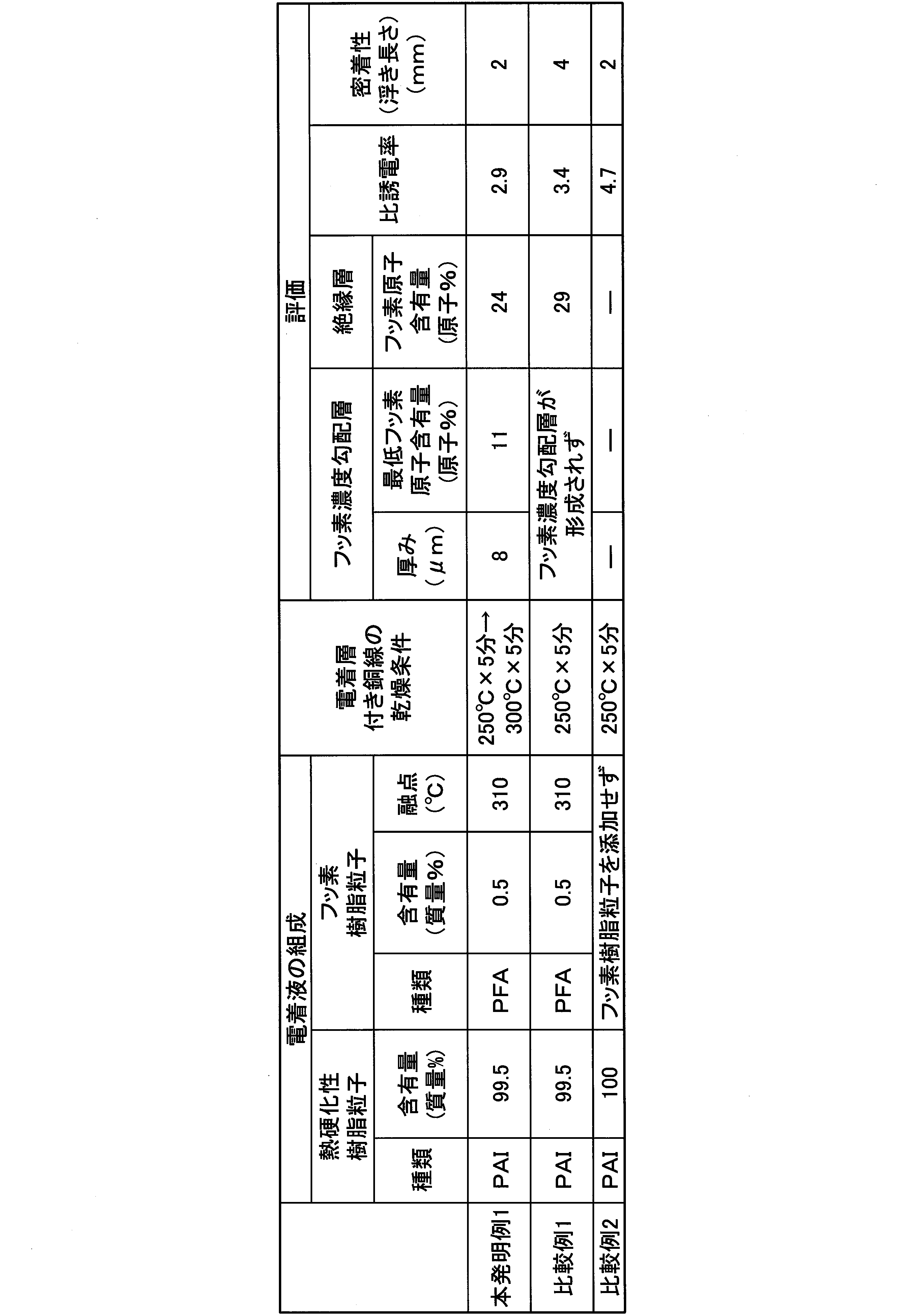
図3Aは、本発明例1で得られた絶縁銅線の絶縁皮膜断面のSEM写真であり、図3Bは、その絶縁皮膜断面のフッ素原子の元素マッピング画像である。図4は、本発明例1で得られた絶縁銅線の絶縁皮膜の厚み方向における元素分布を示すグラフである。元素マッピング画像において白い部分はフッ素原子を示す。図3AのSEM写真と図3Bのフッ素原子の元素マッピング画像から、本発明例1で得られた絶縁銅線では、絶縁皮膜12に、フッ素含有樹脂組成物層13と、導体11とフッ素含有樹脂組成物層13と間に配置されたフッ素濃度勾配層14とが形成されていることが確認された。また、図4のグラフから、フッ素含有樹脂組成物層とフッ素濃度勾配層とは、各元素の分布が連続的に変化しており、連続相を形成していることが確認された。これに対して、電着層付き銅線の乾燥温度が、250℃(PFA粒子の融点に対して-60℃)と低い比較例1で得られた絶縁銅線は、絶縁皮膜にフッ素濃度勾配層が形成されず、絶縁皮膜は絶縁層単層であった。
また、表1に示すように、ポリアミドイミド樹脂およびフッ素樹脂を含む単層の絶縁皮膜を備えた比較例1の絶縁銅線と、ポリアミドイミド樹脂を単独で含む単層の絶縁皮膜を備えた比較例2の絶縁銅線とを比較すると、比誘電率は比較例1の絶縁銅線の方が低くなった。一方、密着性は比較例2の絶縁銅線の方が浮き長さが短く、優れていることが確認された。
これに対して、絶縁皮膜がフッ素濃度勾配層を有する本発明例1の絶縁銅線は、比誘電率は比較例1の絶縁銅線と同様に低く抑えられ、密着性は比較例2の絶縁銅線と同様に高いことが確認された。
これに対して、絶縁皮膜がフッ素濃度勾配層を有する本発明例1の絶縁銅線は、比誘電率は比較例1の絶縁銅線と同様に低く抑えられ、密着性は比較例2の絶縁銅線と同様に高いことが確認された。
(フッ素含有樹脂組成物層の構造)
本発明例1の絶縁銅線について、フッ素含有樹脂組成物層の構造を、SEM-EDS分析装置(日立ハイテク社製、電子顕微鏡SU8230)により確認した。その結果を図5に示す。図5のSEM写真からフッ素含有樹脂組成物層は、ポリアミドイミドを含む海相15と、海相15に散されたフッ素樹脂を含む島相16とから構成された海島構造を有することが確認された。
本発明例1の絶縁銅線について、フッ素含有樹脂組成物層の構造を、SEM-EDS分析装置(日立ハイテク社製、電子顕微鏡SU8230)により確認した。その結果を図5に示す。図5のSEM写真からフッ素含有樹脂組成物層は、ポリアミドイミドを含む海相15と、海相15に散されたフッ素樹脂を含む島相16とから構成された海島構造を有することが確認された。
本発明の絶縁導体は、部分放電開始電圧が高く、かつ絶縁皮膜と導体との密着性に優れ、亀裂が生じにくいので、モータや変圧器などの各種電気機器用の電気コイルとして有利に使用することができる。また、本発明の絶縁導体の製造方法を用いることによって、部分放電開始電圧が高く、かつ絶縁皮膜と導体との密着性に優れ、亀裂が生じにくい絶縁導体を工業的に有利に製造することができる。
10 絶縁導体
11 導体
12 絶縁皮膜
13 フッ素含有樹脂組成物層
14 フッ素濃度勾配層
15 海相
16 島相
11 導体
12 絶縁皮膜
13 フッ素含有樹脂組成物層
14 フッ素濃度勾配層
15 海相
16 島相
Claims (11)
- 導体と、前記導体の表面に備えられた絶縁皮膜とを有する絶縁導体であって、
前記絶縁皮膜は、熱硬化性樹脂の硬化物およびフッ素樹脂を含むフッ素含有樹脂組成物層と、前記導体と前記フッ素含有樹脂組成物層との間に配置された、熱硬化性樹脂の硬化物およびフッ素樹脂を含み、前記フッ素含有樹脂組成物層側から前記導体に向かってフッ素原子含有量が低減する濃度勾配が設けられているフッ素濃度勾配層とを有していることを特徴とする絶縁導体。 - 前記フッ素含有樹脂組成物層に含まれる前記フッ素樹脂は熱可塑性樹脂であり、前記フッ素濃度勾配層に含まれる前記フッ素樹脂は熱可塑性樹脂であることを特徴とする請求項1に記載の絶縁導体。
- 前記フッ素含有樹脂組成物層は、熱硬化性樹脂の硬化物を含む海相と、前記海相に分散されたフッ素樹脂を含む島相とから構成された海島構造を有することを特徴とする請求項1または2に記載の絶縁導体。
- 前記フッ素濃度勾配層中の最もフッ素原子含有量の低い箇所におけるフッ素原子含有量と、前記フッ素含有樹脂組成物層の厚み方向における中央領域のフッ素原子含有量との差が10原子%以上であることを特徴とする請求項1から3のうちいずれか1項に記載の絶縁導体。
- 前記フッ素濃度勾配層中の最もフッ素原子含有量の低い箇所におけるフッ素原子含有量が、15原子%以下であることを特徴とする請求項1から4のうちいずれか1項に記載の絶縁導体。
- 前記フッ素濃度勾配層中の最もフッ素原子含有量の低い箇所が、前記導体の表面から3μm以内の範囲内にあることを特徴とする請求項1から5のうちいずれか1項に記載の絶縁導体。
- 前記フッ素含有樹脂組成物層の厚み方向における中央領域のフッ素原子含有量が20質量%以上70質量%以下の範囲内にあることを特徴とする請求項1から6のうちいずれか1項に記載の絶縁導体。
- 前記フッ素濃度勾配層と前記フッ素含有樹脂組成物層とが連続相であることを特徴とする請求項1から7のうちいずれか1項に記載の絶縁導体。
- 前記フッ素濃度勾配層の厚みが2μm以上15μm以下の範囲内にあることを特徴とする請求項1から8のうちいずれか1項に記載の絶縁導体。
- 請求項1から9のうちいずれか1項に記載の絶縁導体を製造する絶縁導体の製造方法であって、
導体の表面に、熱硬化性樹脂粒子とフッ素樹脂粒子とを含む電着液を電着させて、電着層付き導体を得る電着工程と、
前記電着層付き導体を、前記フッ素樹脂粒子の融点に対して-40℃以上+30℃以下の温度で加熱して乾燥させる乾燥工程と、を含むことを特徴とする絶縁導体の製造方法。 - 前記乾燥工程における加熱時間が5分以上であることを特徴とする請求項10に記載の絶縁導体の製造方法。
Priority Applications (4)
| Application Number | Priority Date | Filing Date | Title |
|---|---|---|---|
| US16/758,505 US11430585B2 (en) | 2017-11-21 | 2018-11-20 | Insulated conductor and insulated conductor manufacturing method |
| CN201880074817.XA CN111418030B (zh) | 2017-11-21 | 2018-11-20 | 绝缘导体及绝缘导体的制造方法 |
| EP18880525.3A EP3716293A4 (en) | 2017-11-21 | 2018-11-20 | INSULATED CONDUCTOR AND METHOD FOR MANUFACTURING AN INSULATED CONDUCTOR |
| KR1020207014087A KR102590076B1 (ko) | 2017-11-21 | 2018-11-20 | 절연 도체 및 절연 도체의 제조 방법 |
Applications Claiming Priority (4)
| Application Number | Priority Date | Filing Date | Title |
|---|---|---|---|
| JP2017223536 | 2017-11-21 | ||
| JP2017-223536 | 2017-11-21 | ||
| JP2018-215925 | 2018-11-16 | ||
| JP2018215925A JP6508406B1 (ja) | 2017-11-21 | 2018-11-16 | 絶縁導体および絶縁導体の製造方法 |
Publications (1)
| Publication Number | Publication Date |
|---|---|
| WO2019102991A1 true WO2019102991A1 (ja) | 2019-05-31 |
Family
ID=66429820
Family Applications (1)
| Application Number | Title | Priority Date | Filing Date |
|---|---|---|---|
| PCT/JP2018/042816 Ceased WO2019102991A1 (ja) | 2017-11-21 | 2018-11-20 | 絶縁導体および絶縁導体の製造方法 |
Country Status (7)
| Country | Link |
|---|---|
| US (1) | US11430585B2 (ja) |
| EP (1) | EP3716293A4 (ja) |
| JP (1) | JP6508406B1 (ja) |
| KR (1) | KR102590076B1 (ja) |
| CN (1) | CN111418030B (ja) |
| TW (1) | TWI787399B (ja) |
| WO (1) | WO2019102991A1 (ja) |
Families Citing this family (4)
| Publication number | Priority date | Publication date | Assignee | Title |
|---|---|---|---|---|
| JP7375777B2 (ja) * | 2021-01-13 | 2023-11-08 | 三菱マテリアル株式会社 | 電着液、絶縁皮膜の製造方法 |
| JP7604977B2 (ja) * | 2021-03-24 | 2024-12-24 | 三菱マテリアル株式会社 | 絶縁皮膜付き平板導電板及びその製造方法 |
| CN113793718B (zh) * | 2021-08-23 | 2024-01-09 | 湖南兴威新材料有限公司 | 一种薄膜电极及其制备方法和应用 |
| CN120527063B (zh) * | 2025-06-27 | 2026-01-13 | 京德电缆有限公司 | 一种耐老化架空绝缘电缆 |
Citations (7)
| Publication number | Priority date | Publication date | Assignee | Title |
|---|---|---|---|---|
| JP2001508588A (ja) * | 1997-01-14 | 2001-06-26 | レイケム・コーポレイション | 絶縁電気導体 |
| JP2003151754A (ja) * | 2001-11-08 | 2003-05-23 | Matsushita Electric Ind Co Ltd | 誘導加熱装置 |
| JP2005259419A (ja) | 2004-03-10 | 2005-09-22 | Matsushita Electric Ind Co Ltd | 絶縁電線およびその製造方法 |
| JP2006004681A (ja) * | 2004-06-16 | 2006-01-05 | Totoku Electric Co Ltd | 温度測定時に好適な着色融着性電線 |
| WO2011024809A1 (ja) | 2009-08-24 | 2011-03-03 | ダイキン工業株式会社 | 電線及びその製造方法 |
| JP2013187029A (ja) | 2012-03-07 | 2013-09-19 | Furukawa Electric Co Ltd:The | 気泡入り絶縁電線の製造方法 |
| JP2017223536A (ja) | 2016-06-15 | 2017-12-21 | 本田技研工業株式会社 | 電池状態推定装置および電池状態推定方法 |
Family Cites Families (10)
| Publication number | Priority date | Publication date | Assignee | Title |
|---|---|---|---|---|
| JPH0237619A (ja) * | 1988-07-27 | 1990-02-07 | Showa Electric Wire & Cable Co Ltd | 耐環境性ケーブル |
| JPH10334739A (ja) * | 1997-05-30 | 1998-12-18 | Hitachi Cable Ltd | 含ふっ素エラストマ被覆電線・ケーブル及びその製造方法 |
| KR100572646B1 (ko) * | 1998-07-17 | 2006-04-24 | 제이에스알 가부시끼가이샤 | 폴리이미드계 복합체 및 이 복합체를 사용한 전자 부품, 및 폴리이미드계 수성 분산액 |
| JP2001294815A (ja) | 2000-04-13 | 2001-10-23 | Jsr Corp | 低誘電率絶縁膜形成用水性分散液、低誘電率絶縁膜および電子部品 |
| JP2002298674A (ja) | 2001-03-29 | 2002-10-11 | Mitsubishi Cable Ind Ltd | 絶縁電線の製造方法および絶縁電線 |
| JP2010100905A (ja) * | 2008-10-24 | 2010-05-06 | Tokai Rubber Ind Ltd | Si含有炭素膜およびこれを用いた型 |
| JP2011071089A (ja) | 2009-08-24 | 2011-04-07 | Daikin Industries Ltd | 電線及びその製造方法 |
| JP6089703B2 (ja) * | 2011-09-14 | 2017-03-08 | 三菱レイヨン株式会社 | プラスチック光ファイバケーブル |
| CN205542046U (zh) * | 2015-03-31 | 2016-08-31 | 日立金属株式会社 | 绝缘电线、磁屏蔽电缆、磁屏蔽管以及磁屏蔽片 |
| JP2019096606A (ja) * | 2017-11-21 | 2019-06-20 | 三菱マテリアル株式会社 | 絶縁導体および絶縁導体の製造方法 |
-
2018
- 2018-11-16 JP JP2018215925A patent/JP6508406B1/ja active Active
- 2018-11-20 EP EP18880525.3A patent/EP3716293A4/en active Pending
- 2018-11-20 WO PCT/JP2018/042816 patent/WO2019102991A1/ja not_active Ceased
- 2018-11-20 KR KR1020207014087A patent/KR102590076B1/ko active Active
- 2018-11-20 US US16/758,505 patent/US11430585B2/en active Active
- 2018-11-20 CN CN201880074817.XA patent/CN111418030B/zh active Active
- 2018-11-21 TW TW107141422A patent/TWI787399B/zh active
Patent Citations (7)
| Publication number | Priority date | Publication date | Assignee | Title |
|---|---|---|---|---|
| JP2001508588A (ja) * | 1997-01-14 | 2001-06-26 | レイケム・コーポレイション | 絶縁電気導体 |
| JP2003151754A (ja) * | 2001-11-08 | 2003-05-23 | Matsushita Electric Ind Co Ltd | 誘導加熱装置 |
| JP2005259419A (ja) | 2004-03-10 | 2005-09-22 | Matsushita Electric Ind Co Ltd | 絶縁電線およびその製造方法 |
| JP2006004681A (ja) * | 2004-06-16 | 2006-01-05 | Totoku Electric Co Ltd | 温度測定時に好適な着色融着性電線 |
| WO2011024809A1 (ja) | 2009-08-24 | 2011-03-03 | ダイキン工業株式会社 | 電線及びその製造方法 |
| JP2013187029A (ja) | 2012-03-07 | 2013-09-19 | Furukawa Electric Co Ltd:The | 気泡入り絶縁電線の製造方法 |
| JP2017223536A (ja) | 2016-06-15 | 2017-12-21 | 本田技研工業株式会社 | 電池状態推定装置および電池状態推定方法 |
Also Published As
| Publication number | Publication date |
|---|---|
| US11430585B2 (en) | 2022-08-30 |
| CN111418030A (zh) | 2020-07-14 |
| KR20200090159A (ko) | 2020-07-28 |
| TW201928997A (zh) | 2019-07-16 |
| US20200251255A1 (en) | 2020-08-06 |
| JP2019096607A (ja) | 2019-06-20 |
| TWI787399B (zh) | 2022-12-21 |
| EP3716293A4 (en) | 2021-08-11 |
| KR102590076B1 (ko) | 2023-10-16 |
| JP6508406B1 (ja) | 2019-05-08 |
| CN111418030B (zh) | 2021-09-10 |
| EP3716293A1 (en) | 2020-09-30 |
Similar Documents
| Publication | Publication Date | Title |
|---|---|---|
| JP6508405B1 (ja) | 絶縁導体および絶縁導体の製造方法 | |
| TWI737892B (zh) | 電鍍液及使用此電鍍液之附絕緣被膜之導體的製造方法 | |
| JP6508406B1 (ja) | 絶縁導体および絶縁導体の製造方法 | |
| JP5423800B2 (ja) | 電線及びその製造方法 | |
| JPWO2018230706A1 (ja) | 絶縁電線 | |
| JP2011071089A (ja) | 電線及びその製造方法 | |
| JP7375777B2 (ja) | 電着液、絶縁皮膜の製造方法 | |
| JP6439062B2 (ja) | 絶縁電線の製造方法 |
Legal Events
| Date | Code | Title | Description |
|---|---|---|---|
| 121 | Ep: the epo has been informed by wipo that ep was designated in this application |
Ref document number: 18880525 Country of ref document: EP Kind code of ref document: A1 |
|
| NENP | Non-entry into the national phase |
Ref country code: DE |
|
| ENP | Entry into the national phase |
Ref document number: 2018880525 Country of ref document: EP Effective date: 20200622 |