WO2019106826A1 - カルテシアンフィードバック回路 - Google Patents
カルテシアンフィードバック回路 Download PDFInfo
- Publication number
- WO2019106826A1 WO2019106826A1 PCT/JP2017/043274 JP2017043274W WO2019106826A1 WO 2019106826 A1 WO2019106826 A1 WO 2019106826A1 JP 2017043274 W JP2017043274 W JP 2017043274W WO 2019106826 A1 WO2019106826 A1 WO 2019106826A1
- Authority
- WO
- WIPO (PCT)
- Prior art keywords
- signal
- circuit
- inverse characteristic
- cartesian feedback
- compensation
- Prior art date
- Legal status (The legal status is an assumption and is not a legal conclusion. Google has not performed a legal analysis and makes no representation as to the accuracy of the status listed.)
- Ceased
Links
Images




Classifications
-
- H—ELECTRICITY
- H04—ELECTRIC COMMUNICATION TECHNIQUE
- H04L—TRANSMISSION OF DIGITAL INFORMATION, e.g. TELEGRAPHIC COMMUNICATION
- H04L27/00—Modulated-carrier systems
- H04L27/32—Carrier systems characterised by combinations of two or more of the types covered by groups H04L27/02, H04L27/10, H04L27/18 or H04L27/26
- H04L27/34—Amplitude- and phase-modulated carrier systems, e.g. quadrature-amplitude modulated carrier systems
- H04L27/38—Demodulator circuits; Receiver circuits
- H04L27/3809—Amplitude regulation arrangements
-
- H—ELECTRICITY
- H03—ELECTRONIC CIRCUITRY
- H03F—AMPLIFIERS
- H03F1/00—Details of amplifiers with only discharge tubes, only semiconductor devices or only unspecified devices as amplifying elements
- H03F1/34—Negative-feedback-circuit arrangements with or without positive feedback
-
- H—ELECTRICITY
- H03—ELECTRONIC CIRCUITRY
- H03F—AMPLIFIERS
- H03F1/00—Details of amplifiers with only discharge tubes, only semiconductor devices or only unspecified devices as amplifying elements
- H03F1/38—Positive-feedback circuit arrangements without negative feedback
-
- H—ELECTRICITY
- H03—ELECTRONIC CIRCUITRY
- H03F—AMPLIFIERS
- H03F3/00—Amplifiers with only discharge tubes or only semiconductor devices as amplifying elements
- H03F3/189—High-frequency amplifiers, e.g. radio frequency amplifiers
-
- H—ELECTRICITY
- H03—ELECTRONIC CIRCUITRY
- H03F—AMPLIFIERS
- H03F3/00—Amplifiers with only discharge tubes or only semiconductor devices as amplifying elements
- H03F3/189—High-frequency amplifiers, e.g. radio frequency amplifiers
- H03F3/19—High-frequency amplifiers, e.g. radio frequency amplifiers with semiconductor devices only
-
- H—ELECTRICITY
- H04—ELECTRIC COMMUNICATION TECHNIQUE
- H04B—TRANSMISSION
- H04B1/00—Details of transmission systems, not covered by a single one of groups H04B3/00 - H04B13/00; Details of transmission systems not characterised by the medium used for transmission
- H04B1/02—Transmitters
- H04B1/04—Circuits
-
- H—ELECTRICITY
- H04—ELECTRIC COMMUNICATION TECHNIQUE
- H04B—TRANSMISSION
- H04B3/00—Line transmission systems
- H04B3/02—Details
- H04B3/04—Control of transmission; Equalising
-
- H—ELECTRICITY
- H04—ELECTRIC COMMUNICATION TECHNIQUE
- H04L—TRANSMISSION OF DIGITAL INFORMATION, e.g. TELEGRAPHIC COMMUNICATION
- H04L27/00—Modulated-carrier systems
- H04L27/32—Carrier systems characterised by combinations of two or more of the types covered by groups H04L27/02, H04L27/10, H04L27/18 or H04L27/26
- H04L27/34—Amplitude- and phase-modulated carrier systems, e.g. quadrature-amplitude modulated carrier systems
- H04L27/36—Modulator circuits; Transmitter circuits
-
- H—ELECTRICITY
- H03—ELECTRONIC CIRCUITRY
- H03F—AMPLIFIERS
- H03F2200/00—Indexing scheme relating to amplifiers
- H03F2200/336—A I/Q, i.e. phase quadrature, modulator or demodulator being used in an amplifying circuit
-
- H—ELECTRICITY
- H03—ELECTRONIC CIRCUITRY
- H03F—AMPLIFIERS
- H03F2200/00—Indexing scheme relating to amplifiers
- H03F2200/451—Indexing scheme relating to amplifiers the amplifier being a radio frequency amplifier
-
- H—ELECTRICITY
- H03—ELECTRONIC CIRCUITRY
- H03F—AMPLIFIERS
- H03F2201/00—Indexing scheme relating to details of amplifiers with only discharge tubes, only semiconductor devices or only unspecified devices as amplifying elements covered by H03F1/00
- H03F2201/32—Indexing scheme relating to modifications of amplifiers to reduce non-linear distortion
Definitions
- the present invention relates to a Cartesian feedback circuit including a loop filter for limiting a signal band.
- An amplifier used for communication generally has non-linearity in which distortion occurs in the signal waveform when amplifying the signal. Since communication requires linear signal transmission, a distortion compensation circuit is used to compensate for distortion generated by the amplifier.
- the distortion compensation circuit is classified into a negative feedback distortion compensation circuit, a feedforward distortion compensation circuit, or a predistortion distortion compensation circuit.
- Patent Document 1 discloses a Cartesian feedback circuit which is a specific circuit of a negative feedback distortion compensation circuit.
- the Cartesian feedback circuit disclosed in Patent Document 1 includes a subtractor and a band limiting circuit.
- the subtractor subtracts a feedback baseband signal obtained by branching a part of the quadrature modulation signal output from the non-linear amplifier from the input baseband signal to obtain a subtraction baseband signal.
- the band limiting circuit performs band limiting of the subtraction baseband signal.
- the subtractor and the band limiting circuit constitute a so-called loop filter.
- Cartesian feedback circuit is a negative feedback distortion compensation circuit, it is necessary to have a loop gain over the entire band when applied to an amplifier for amplifying a wide band modulation wave signal.
- positive feedback may be applied at a certain frequency to cause oscillation, and distortion generated by the amplifier can not be compensated. is there.
- the loop gain of the Cartesian feedback circuit is set to a value within a range in which positive feedback does not occur over the entire wide band, only a distortion compensation amount smaller than a desired distortion compensation amount can be obtained, Can not compensate enough for the distortion generated by For this reason, in the conventional Cartesian feedback circuit, when the loop gain is increased to obtain a desired distortion compensation amount, it is necessary to band-limit using a loop filter.
- band limiting is performed using a loop filter in the conventional Cartesian feedback circuit, distortion is compensated by the fact that the gain is dropped around the cutoff frequency of the filter due to the influence of the frequency characteristic of the loop filter and the phase is delayed. There is a problem that the amount is smaller than the loop gain.
- the present invention has been made to solve the problems as described above, and it is an object of the present invention to obtain a Cartesian feedback circuit which does not cause a change in gain and a change in phase due to a loop filter.
- the Cartesian feedback circuit comprises a differential I signal which is a difference between a first I signal which is an in-phase component of a modulation wave signal and a second I signal which is an in-phase component of an amplified harmonic signal.
- a difference Q between a first loop filter circuit that limits the signal band, a first Q signal that is the quadrature phase component of the modulation wave signal, and a second Q signal that is the quadrature phase component of the harmonic signal
- a second loop filter circuit for limiting the signal band of the signal, a quadrature modulator for generating a harmonic signal from the differential I signal whose signal band is limited and the differential Q signal whose signal band is limited, and a quadrature modulator
- An amplifier for amplifying the generated harmonic signal, an orthogonal demodulator for demodulating the second I signal and the second Q signal from the harmonic signal amplified by the amplifier, and an inverse characteristic of the first loop filter circuit Frequency of And a second inverse characteristic circuit having a frequency characteristic inverse to the second loop
- the first I signal having passed through the first inverse characteristic circuit having frequency characteristics inverse to the first loop filter circuit is output to the first loop filter circuit
- the second loop filter Since the first Q signal that has passed through the second inverse characteristic circuit having a frequency characteristic opposite to that of the circuit is output to the second loop filter circuit, the change in gain and phase caused by the loop filter There is an effect that it is possible to obtain a Cartesian feedback circuit which does not occur.
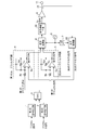
- FIG. 1 is a configuration diagram showing a Cartesian feedback circuit according to a first embodiment.
- FIG. 2A is a Bode diagram when the loop gain of the Cartesian feedback circuit is 15 dB
- FIG. 2B is a Bode diagram when the gains of the operational amplifiers 4a and 5a are increased to 30 dB.
- FIG. 6 is an explanatory view showing a relationship between a ratio of a cutoff frequency of the first loop filter circuit 4 and the second loop filter circuit 5 to an upper limit frequency in a signal band of a modulation wave signal, and a distortion compensation amount.
- FIG. 7 is a block diagram showing a Cartesian feedback circuit according to a second embodiment.
- FIG. 13 is a block diagram showing a Cartesian feedback circuit according to a third embodiment.
- FIG. 14 is a configuration diagram showing a Cartesian feedback circuit according to a fourth embodiment.
- FIG. 18 is a configuration diagram showing a Cartesian feedback circuit according to a fifth embodiment.
- FIG. 18 is a block diagram showing another Cartesian feedback circuit according to the fifth embodiment.
- FIG. 1 is a block diagram showing a Cartesian feedback circuit according to a first embodiment.
- a first inverse characteristic circuit 1 is a digital filter that receives a first I signal, which is an in-phase component of a modulation wave signal.
- the first I signal is a digital signal and is hereinafter referred to as a digital I signal.
- the first inverse characteristic circuit 1 has a frequency characteristic that is the inverse characteristic of the first loop filter circuit 4, and as a digital filter, a complex FIR (Finite Impulse Response) filter or a complex IIR (Infinite Impulse Response) filter, etc. Is used.
- the second inverse characteristic circuit 2 is a digital filter that receives a first Q signal that is a quadrature phase component of the modulation wave signal.
- the first Q signal is a digital signal and is hereinafter referred to as a digital Q signal.
- the second inverse characteristic circuit 2 has a frequency characteristic that is the inverse characteristic of the second loop filter circuit 5, and a complex FIR filter or complex IIR filter or the like is used as a digital filter.
- the DAC 3 which is a digital-to-analog converter converts the digital I signal that has passed through the first inverse characteristic circuit 1 into an analog signal (hereinafter referred to as a first analog I signal), and converts the first analog I signal into a first signal. Output to the loop filter circuit 4 of FIG. Also, the DAC 3 converts the digital Q signal that has passed through the second inverse characteristic circuit 2 into an analog signal (hereinafter, referred to as a first analog Q signal), and the first analog Q signal as a second loop filter circuit Output to 5
- the first loop filter circuit 4 is a loop filter including an operational amplifier 4a, resistors 4b and 4c, and a capacitor 4d.
- the first loop filter circuit 4 limits the signal band of the differential I signal which is the difference between the first analog I signal output from the DAC 3 and the second analog I signal output from the quadrature demodulator 12. This is a circuit that outputs the differential I signal after band limitation to the quadrature modulator 8.
- the first inverse characteristic circuit 1 having the frequency characteristic having the inverse characteristic to the first loop filter circuit 4 is provided, the first loop filter circuit 4 has its own frequency characteristic. Even when distortion is caused in the differential I signal, the differential I signal output from the first loop filter circuit 4 does not have frequency characteristics, and both the amplitude and the phase are flat. Become.
- the operational amplifier 4 a receives the first analog I signal input and the second analog I output from the quadrature demodulator 12. It is a differential amplifier that amplifies the difference I signal that is the difference from the signal.
- One end of the resistor 4 b is connected to the output side of the DAC 3, and the other end is connected to the ⁇ input terminal of the operational amplifier 4 a.
- One end of the resistor 4c is connected to the-input terminal of the operational amplifier 4a, and the other end is connected to the output terminal of the operational amplifier 4a.
- One end of the capacitor 4d is connected to the-input terminal of the operational amplifier 4a, and the other end is connected to the output terminal of the operational amplifier 4a.
- the signal band of the differential I signal amplified by the operational amplifier 4a is limited by the resistor 4c and the capacitor 4d.
- Gain of the operational amplifier 4a is determined by the ratio R 2 / R 1 of the resistance value R 2 of the resistance value R 1 and the resistor 4c of the resistor 4b, the cut-off frequency of the loop filter is a first loop filter circuit 4, It is determined by the capacitance value of the capacitor 4d. The cutoff frequency decreases as the capacitance value of the capacitor 4d increases.
- the second loop filter circuit 5 is a loop filter including an operational amplifier 5a, resistors 5b and 5c, and a capacitor 5d.
- the second loop filter circuit 5 limits the signal band of the differential Q signal which is the difference between the first analog Q signal output from the DAC 3 and the second analog Q signal output from the quadrature demodulator 12. This is a circuit that outputs the differential Q signal after band limitation to the quadrature modulator 8.
- the second inverse characteristic circuit 2 having the frequency characteristic having the inverse characteristic to the second loop filter circuit 5 is provided, the second loop filter circuit 5 has its own frequency characteristic. Even when distortion is caused in the differential Q signal, the differential Q signal output from the second loop filter circuit 5 does not have frequency characteristics, and both the amplitude and the phase are flat. Become.
- the operational amplifier 5 a receives the first analog Q signal input and the second analog Q output from the quadrature demodulator 12. It is a differential amplifier that amplifies a differential Q signal that is the difference from the signal.
- One end of the resistor 5 b is connected to the output side of the DAC 3, and the other end is connected to the ⁇ input terminal of the operational amplifier 5 a.
- One end of the resistor 5c is connected to the-input terminal of the operational amplifier 5a, and the other end is connected to the output terminal of the operational amplifier 5a.
- One end of the capacitor 5d is connected to the-input terminal of the operational amplifier 5a, and the other end is connected to the output terminal of the operational amplifier 5a.
- the signal band of the differential Q signal amplified by the operational amplifier 5a is limited by the resistor 5c and the capacitor 5d.
- Gain of the operational amplifier 5a is determined by the ratio R 4 / R 3 of the resistance value R 3 of the resistor 5b and the resistance value R 4 of the resistors 5c
- the cutoff frequency of the loop filter is a second loop filter circuit 5, It is determined by the capacitance value of the capacitor 5d. The cutoff frequency is lower as the capacitance value of the capacitor 5d is larger.
- the local oscillation source 6 is a signal source that outputs a local oscillation signal.
- Phase shifter 7 has a phase of a local oscillation signal output from local oscillation source 6 according to a group delay time which is a sum of respective delay times in quadrature modulator 8, amplifier 9, coupler 10 and quadrature demodulator 12. , And outputs the local oscillation signal after phase adjustment to the quadrature demodulator 12.
- the quadrature modulator 8 generates a modulation wave signal from the differential I signal whose signal band is limited by the first loop filter circuit 4 and the differential Q signal whose signal band is limited by the second loop filter circuit 5. .
- the quadrature modulator 8 generates a harmonic signal (hereinafter referred to as an RF signal) by converting the frequency of the generated modulation wave signal using the local oscillation signal output from the local oscillation source 6. , The generated RF signal is output to the amplifier 9.
- an RF signal a harmonic signal
- the amplifier 9 amplifies the RF signal output from the quadrature modulator 8 and outputs the amplified RF signal to the coupler 10.
- the coupler 10 outputs the RF signal output from the quadrature modulator 8 to the output terminal 11. Further, when outputting the RF signal to the output terminal 11, the coupler 10 outputs a part of the RF signal to the quadrature demodulator 12.
- the output terminal 11 is a terminal for outputting the RF signal output from the quadrature modulator 8 to the outside.
- the quadrature demodulator 12 generates the modulation wave signal by converting the frequency of the RF signal output from the coupler 10 using the local oscillation signal output from the phase shifter 7.
- the quadrature demodulator 12 demodulates the analog I signal (hereinafter referred to as a second analog I signal) and the analog Q signal (hereinafter referred to as a second analog Q signal) from the generated modulated wave signal.
- the quadrature demodulator 12 outputs the demodulated second analog I signal to the first loop filter circuit 4, and outputs the demodulated second analog Q signal to the second loop filter circuit 5.
- the first inverse characteristic circuit 1 has frequency characteristics that are inverse to the first loop filter circuit 4.
- the second inverse characteristic circuit 2 has frequency characteristics that are inverse to the second loop filter circuit 5.
- the frequency characteristic of the first loop filter circuit 4 and the frequency characteristic of the second loop filter circuit 5 have the characteristic that the amplitude on the high frequency side decreases and the phase on the high frequency side is delayed. ing. Therefore, as shown in FIG. 1, the frequency characteristic of the first inverse characteristic circuit 1 and the frequency characteristic of the second inverse characteristic circuit 2 are characteristic that the amplitude on the high frequency side increases and the phase on the high frequency side advances. have.
- the digital I signal input to the first inverse characteristic circuit 1 has no frequency characteristic, and both the amplitude and the phase are flat.
- the digital Q signal input to the second inverse characteristic circuit 2 also has no frequency characteristic, and both the amplitude and the phase are flat.
- the DAC 3 converts the digital I signal output from the first inverse characteristic circuit 1 into an analog signal, and outputs the first analog I signal to the first loop filter circuit 4. Also, the DAC 3 converts the digital Q signal output from the second inverse characteristic circuit 2 into an analog signal, and outputs the first analog Q signal to the second loop filter circuit 5.
- the first loop filter circuit 4 limits the signal band of the differential I signal which is the difference between the first analog I signal output from the DAC 3 and the second analog I signal output from the quadrature demodulator 12. , The band-limited differential I signal is output to the quadrature modulator 8.
- the first loop filter circuit 4 since the first inverse characteristic circuit 1 having the frequency characteristic having the inverse characteristic to the first loop filter circuit 4 is provided, the first loop filter circuit 4 has its own frequency characteristic. Even when distortion is caused in the differential I signal, the differential I signal output from the first loop filter circuit 4 does not have frequency characteristics, and both the amplitude and the phase are flat. Become.
- the first loop filter circuit 4, the quadrature modulator 8, the amplifier 9, the coupler 10 and the quadrature demodulator 12 constitute a feedback loop, and the feedback loop is applied to the negative feedback.
- the distortion component contained in the second analog I signal output from V.sub.2 is reduced.
- distortion components included in the RF signal output from the amplifier 9 are reduced.
- the second loop filter circuit 5 limits the signal band of the differential Q signal which is the difference between the first analog Q signal output from the DAC 3 and the second analog Q signal output from the quadrature demodulator 12. , The band-limited differential Q signal is output to the quadrature modulator 8.
- the second loop filter circuit 5 since the second inverse characteristic circuit 2 having the frequency characteristic having the inverse characteristic to the second loop filter circuit 5 is provided, the second loop filter circuit 5 has its own frequency characteristic. Even when distortion is caused in the differential Q signal, the differential Q signal output from the second loop filter circuit 5 does not have frequency characteristics, and both the amplitude and the phase are flat. Become.
- the feedback loop is constituted by the second loop filter circuit 5, the quadrature modulator 8, the amplifier 9, the coupler 10 and the quadrature demodulator 12, and negative feedback is applied in the feedback loop.
- the distortion component contained in the second analog Q signal output from V.sub.2 is reduced.
- distortion components included in the RF signal output from the amplifier 9 are reduced.
- the local oscillation source 6 oscillates a local oscillation signal and outputs the local oscillation signal to the phase shifter 7 and the quadrature modulator 8.
- phase shifter 7 receives a local oscillation signal from local oscillation source 6, phase adjuster 7 adjusts the phase of the local oscillation signal according to the group delay time in quadrature modulator 8, amplifier 9, coupler 10 and quadrature demodulator 12.
- the local oscillation signal after the phase adjustment is output to the quadrature demodulator 12.
- the quadrature modulator 8 generates a modulation wave signal from the difference I signal output from the first loop filter circuit 4 and the difference Q signal output from the second loop filter circuit 5. Further, the quadrature modulator 8 converts the frequency of the generated modulation wave signal using the local oscillation signal output from the local oscillation source 6 to generate an RF signal which is a harmonic signal, and generates an RF signal. Output to the amplifier 9.
- the amplifier 9 When the amplifier 9 receives the RF signal from the quadrature modulator 8, the amplifier 9 amplifies the RF signal and outputs the amplified RF signal to the coupler 10.
- the coupler 10 outputs the RF signal output from the quadrature modulator 8 to the output terminal 11. Further, when outputting the RF signal to the output terminal 11, the coupler 10 outputs a part of the RF signal to the quadrature demodulator 12.
- the quadrature demodulator 12 When the quadrature demodulator 12 receives the RF signal from the coupler 10, the quadrature demodulator 12 converts the frequency of the RF signal using the local oscillation signal output from the phase shifter 7 to generate a modulation wave signal. Further, the quadrature demodulator 12 demodulates the second analog I signal and the second analog Q signal from the generated modulated wave signal, and demodulates the demodulated second analog I signal to the first loop filter circuit 4. The second analog Q signal output and demodulated is output to the second loop filter circuit 5.
- FIG. 2 is a Bode diagram showing the performance of the Cartesian feedback circuit of FIG.
- the Bode diagram of FIG. 2 shows the gain and phase characteristics of the closed loop in the Cartesian feedback circuit of FIG.
- FIG. 2A shows a Bode diagram when the loop gain of the Cartesian feedback circuit is 15 dB, and the phase characteristic shows the case where the group delay time of the closed loop circuit is 15 ns.
- the group delay time of the closed loop circuit is determined by the sum of the group delay times in the first loop filter circuit 4, the second loop filter circuit 5, the quadrature modulator 8, the amplifier 9, the coupler 10 and the quadrature demodulator 12.
- FIG. 2B shows a Bode diagram when the gains of the operational amplifiers 4a and 5a are increased to 30 dB.
- the loop gain of the Cartesian feedback circuit is determined by the gains of the operational amplifiers 4a and 5a and the losses generated in the quadrature modulator 8, the amplifier 9, the coupler 10, the quadrature demodulator 12 and the line, respectively.
- a line is a line connecting between components of a closed loop circuit.
- the circuit of the closed loop does not include an attenuator or variable attenuator, but the attenuator or variable attenuator may be used to adjust the loop gain.
- the loop gain of the Cartesian feedback circuit is determined in consideration of the loss caused by the attenuator or variable attenuator.
- the phase when the loop gain of the Cartesian feedback circuit is 0 dB is ⁇ 105 deg and does not lag behind ⁇ 180 deg. Therefore, oscillation due to positive feedback does not occur.
- the phase margin is required to be about 40 deg to 80 deg in consideration of temperature variations and element variations.
- the loop gain of the Cartesian feedback circuit is increased at the expense of the phase margin. Do.
- FIG. 3 is an explanatory drawing showing the relationship between the ratio of the cutoff frequency of the first loop filter circuit 4 and the second loop filter circuit 5 to the upper limit frequency in the signal band of the modulation wave signal, and the distortion compensation amount.
- the signal band of the modulation wave signal is the base band and the signal band is from 0 to the upper limit frequency.
- the Cartesian feedback circuit does not include the first inverse characteristic circuit 1 and the second inverse characteristic circuit 2, as shown in FIG. 3, the upper limit frequency in the signal band of the modulation wave signal is 2 of the cutoff frequency. If the frequency is higher than the doubled frequency, the distortion compensation amount drops below 15 dB.
- the cause of the decrease in the distortion compensation amount is that the gain of the modulation wave signal is dropped around the cutoff frequency of the first loop filter circuit 4 and the second loop filter circuit 5 and the phase is changed.
- the frequency characteristic occurs in the signal band of (1), and as a result, distortion occurs and the modulation accuracy is reduced.
- the Cartesian feedback circuit includes the first inverse characteristic circuit 1 and the first inverse characteristic circuit 1 in order to prevent the distortion compensation amount and the modulation accuracy from being lowered while the phase shift margin of 75 deg is maintained.
- the change in the phase and the gain of the modulation wave signal are prevented from falling around the cutoff frequency of the first loop filter circuit 4 and the second loop filter circuit 5.
- the Cartesian feedback circuit includes the first inverse characteristic circuit 1 and the second inverse characteristic circuit 2, as shown in FIG. 3, the upper limit frequency within the signal band of the modulation wave signal is 2 as the cutoff frequency. Even if the frequency is higher than the doubled frequency, a distortion compensation amount of 15 dB is obtained.
- the Cartesian feedback circuit includes the first inverse characteristic circuit 1 and the second inverse characteristic circuit 2 so that the first inverse characteristic circuit 1 and the second inverse characteristic circuit 2 are not provided.
- the reason why distortion components can be compensated in a wide band will be described.
- the Cartesian feedback circuit does not include the first inverse characteristic circuit 1 and the second inverse characteristic circuit 2
- the first analog I signal and the first analog Q signal output from the DAC 3 have frequencies There is no characteristic, and both the amplitude and the phase become flat.
- Each of the first analog I signal and the first analog Q signal output from the DAC 3 is input to the first loop filter circuit 4 and the second loop filter circuit 5 to generate the first loop filter circuit 4 and the first loop filter circuit 4.
- the differential I signal and the differential I signal and the differential Q signal are output when the upper limit frequency in the signal band of the modulation wave signal is equal to or higher than twice the cutoff frequency.
- the amplitude on the high frequency side of each signal band of the differential Q signal decreases, and the phase on the high frequency side is delayed. Therefore, the amplitude and phase of the differential I signal output from the first loop filter circuit 4 deviates from the amplitude and phase of the first analog I signal output from the DAC 3. Further, the amplitude and the phase of the differential Q signal output from the second loop filter circuit 5 deviate from the amplitude and the phase of the first analog Q signal output from the DAC 3.
- the differential I signal and the differential Q signal having a shift in amplitude and phase respectively output from the first loop filter circuit 4 and the second loop filter circuit 5 pass through the quadrature modulator 8 and the amplifier 9, where Further distortion occurs in the amplifier 9 in the differential I signal and the differential Q signal.
- Portions of the differential I signal and the differential Q signal in which distortion is caused pass through the quadrature demodulator 12 and are used as the second analog I signal and the second analog Q signal to generate the first loop filter circuit 4 and the second loop filter circuit 4. It is fed back to the loop filter circuit 5.
- the fed back second analog I signal and second analog Q signal, the first analog I signal output from the DAC 3, and the first And the distortion components included in the differential I signal and the differential Q signal are compensated by the distortion compensation amount corresponding to the loop gain.
- the distortion compensation amount corresponding to the loop gain hardly decreases if the upper limit frequency in the signal band of the modulation wave signal is lower than the frequency twice the cutoff frequency.
- the distortion compensation amount and the modulation accuracy decrease with the decrease of the amplitude on the high frequency side and the phase delay.
- the amount by which the distortion component included in the differential I signal and the differential Q signal can be compensated is reduced, and the distortion component can not be compensated sufficiently.
- the Cartesian feedback circuit includes the first inverse characteristic circuit 1 and the second inverse characteristic circuit 2
- the digital output from the first inverse characteristic circuit 1 and the second inverse characteristic circuit 2 The I signal and the digital Q signal have frequency characteristics in which the amplitude on the high frequency side is increased and the phase on the high frequency side is advanced.
- Each of the first analog I signal and the first analog Q signal output from the DAC 3 is input to the first loop filter circuit 4 and the second loop filter circuit 5, and the first loop filter circuit 4 and the first loop filter circuit 5 are
- the differential I signal and the differential Q signal are output from the second loop filter circuit 5, the differential I signal and the differential Q signal have frequency characteristics and a second frequency characteristic that are reverse to the first inverse characteristic circuit 1.
- each of the differential I signal output from the first loop filter circuit 4 and the differential Q signal output from the second loop filter circuit 5 does not have frequency characteristics, and both the amplitude and phase are It has flat characteristics.
- the differential I signal and the differential Q signal not having frequency characteristics pass through the quadrature modulator 8 and the amplifier 9, and at that time, distortion occurs in the amplifier 9 in the differential I signal and the differential Q signal. .
- Portions of the differential I signal and the differential Q signal in which distortion is caused pass through the quadrature demodulator 12 and are used as the second analog I signal and the second analog Q signal to generate the first loop filter circuit 4 and the second loop filter circuit 4. It is fed back to the loop filter circuit 5.
- the fed back second analog I signal and second analog Q signal, the first analog I signal output from the DAC 3, and the first And the distortion components included in the differential I signal and the differential Q signal are compensated by the distortion compensation amount corresponding to the loop gain.
- the Cartesian feedback circuit includes the first inverse characteristic circuit 1 and the second inverse characteristic circuit 2, the differential I signal output from the first loop filter circuit 4 and the second loop filter circuit 5
- Each of the output differential Q signals does not have frequency characteristics, and both amplitude and phase become flat characteristics. Therefore, the distortion compensation amount does not decrease even when the upper limit frequency in the signal band of the modulation wave signal is equal to or higher than the frequency twice the cutoff frequency. Therefore, in the case where the first inverse characteristic circuit 1 and the second inverse characteristic circuit 2 are provided, it is larger in a wider band than in the case where the first inverse characteristic circuit 1 and the second inverse characteristic circuit 2 are not provided. Since the distortion compensation amount is obtained, distortion components included in the differential I signal and the differential Q signal can be compensated.
- the first I signal that has passed through the first inverse characteristic circuit 1 having the frequency characteristic of the inverse characteristic to the first loop filter circuit 4 is output to the first loop filter circuit 4.
- the first Q signal that has passed through the second inverse characteristic circuit 2 having a frequency characteristic reverse to that of the second loop filter circuit 5 is output to the second loop filter circuit 5. Therefore, it is possible to obtain a Cartesian feedback circuit in which a change in gain and a change in phase due to a loop filter do not occur.
- the inverse characteristic circuit 1 and the second inverse characteristic circuit 2 may have frequency characteristics that are inverse to the first loop filter circuit 4 and the second loop filter circuit 5, respectively.
- the respective frequency characteristics of the first inverse characteristic circuit 1 and the second inverse characteristic circuit 2 are set to the first loop filter circuit 4 and the first loop filter circuit 4 up to a frequency approximately twice the upper limit frequency within the signal band of the modulation wave signal.
- the second loop filter circuit 5 has frequency characteristics that are reverse to those of each of the second loop filter circuits 5, there is no frequency at which the distortion compensation amount deteriorates in the signal band.
- the Cartesian feedback circuit includes the first inverse characteristic circuit 1 having frequency characteristics inverse to the first loop filter circuit 4 and the inverse characteristic of the second loop filter circuit 5. And a second inverse characteristic circuit 2 having a frequency characteristic of
- the coefficient of the complex FIR filter or the coefficient of the complex IIR filter in the first inverse characteristic circuit 1 is adjusted according to the frequency characteristic of the first loop filter circuit 4 and the second inverse characteristic circuit
- An example in which the coefficients of the complex FIR filter or the coefficients of the complex IIR filter in 2 are adjusted in accordance with the frequency characteristic of the second loop filter circuit 5 will be described.
- FIG. 4 is a block diagram showing a Cartesian feedback circuit according to a second embodiment.
- the first loop filter circuit 4 includes a variable resistor 4e instead of the resistor 4c, and a variable capacitor 4f instead of the capacitor 4d.
- the second loop filter circuit 5 includes a variable resistor 5e instead of the resistor 5c, and a variable capacitor 5f instead of the capacitor 5d.
- the first coefficient adjustment circuit 21 is the first inverse characteristic circuit 1 being a complex FIR filter or complex IIR filter, the coefficient or complex IIR filter of the complex FIR filter corresponding to the frequency characteristic of the first loop filter circuit 4 And a look-up table (hereinafter referred to as a LUT) 21a storing coefficients of The first coefficient adjustment circuit 21 refers to the coefficient of the complex FIR filter or the coefficient of the complex IIR filter in the first inverse characteristic circuit 1 and the coefficient corresponding to the frequency characteristic of the first loop filter circuit 4 with reference to the LUT 21 a. Adjust to
- the second coefficient adjustment circuit 22 is such that the second inverse characteristic circuit 2 is a complex FIR filter or complex IIR filter
- the coefficient or complex IIR filter of the complex FIR filter corresponding to the frequency characteristic of the second loop filter circuit 5 Is provided with a LUT 22a storing coefficients of
- the second coefficient adjustment circuit 22 refers to the coefficient of the complex FIR filter or the coefficient of the complex IIR filter in the second inverse characteristic circuit 2 and the coefficient corresponding to the frequency characteristic of the second loop filter circuit 5 with reference to the LUT 22a.
- changing the frequency characteristics by adjusting the coefficients of the complex FIR filter or the coefficients of the complex IIR filter is a known technique, and thus the detailed description is omitted.
- the signal band of the modulation wave signal including the digital I signal and the digital Q signal may be different for each communication system. Therefore, if it is possible to change each of the frequency characteristic of the first loop filter circuit 4 and the frequency characteristic of the second loop filter circuit 5, applying the Cartesian feedback circuit to many communication systems it can. Therefore, in the second embodiment, as the frequency characteristics of the first loop filter circuit 4, the first gain can be adjusted so that the loop gain determined by the gain of the operational amplifier 4 a and the cutoff frequency of the first loop filter circuit 4 can be adjusted.
- the loop filter circuit 4 includes a variable resistor 4e and a variable capacitor 4f. Further, the second loop filter circuit 5 can adjust the loop gain determined by the gain of the operational amplifier 5a and the cut-off frequency of the second loop filter circuit 5 as the frequency characteristics of the second loop filter circuit 5, A variable resistor 5e and a variable capacitor 5f are provided.
- the first inverse characteristic circuit 1 when the frequency characteristic of the first loop filter circuit 4 is changed, the first inverse characteristic circuit 1 has an inverse characteristic to the frequency characteristic of the first loop filter circuit 4.
- the first coefficient adjusting circuit 21 is provided in order to have frequency characteristics.
- second inverse characteristic circuit 2 when the frequency characteristic of second loop filter circuit 5 is changed, second inverse characteristic circuit 2 is opposite to the frequency characteristic of second loop filter circuit 5.
- a second coefficient adjustment circuit 22 is provided to have a characteristic frequency characteristic.
- the coefficient or complex IIR filter of the complex FIR filter corresponding to the frequency characteristic of the first loop filter circuit 4 Is provided with a LUT 21a storing coefficients of.
- the LUT 21a as a coefficient of a complex FIR filter corresponding to the frequency characteristic of the first loop filter circuit 4 or a coefficient of a complex IIR filter, corresponds to a coefficient corresponding to a combination of the resistance value of the variable resistor 4e and the capacitance value of the variable capacitor 4f.
- the first coefficient adjustment circuit 21 refers to the LUT 21a to acquire the coefficient of the complex FIR filter or the coefficient of the complex IIR filter corresponding to the combination of the resistance value of the variable resistor 4e and the capacitance value of the variable capacitor 4f.
- Each of the resistance value of the variable resistor 4e and the capacitance value of the variable capacitor 4f may be manually given to the first coefficient adjustment circuit 21 by the user, or may be adjusted by communication from an external device or the like. It may be provided to the circuit 21.
- the first coefficient adjustment circuit 21 sets the frequency coefficient of the first coefficient adjustment circuit 21 by setting the coefficient of the complex FIR filter or the coefficient of the complex IIR filter in the first loop filter circuit 4 to the acquired coefficient.
- the frequency characteristic of the first loop filter circuit 4 is set opposite to that of the first loop filter circuit 4.
- the coefficient or complex IIR filter of the complex FIR filter corresponding to the frequency characteristic of the second loop filter circuit 5 Is provided with a LUT 22a storing coefficients of The LUT 22a uses a coefficient corresponding to the combination of the resistance value of the variable resistor 5e and the capacitance value of the variable capacitor 5f as a coefficient of a complex FIR filter corresponding to the frequency characteristic of the second loop filter circuit 5 or a coefficient of a complex IIR filter.
- the second coefficient adjustment circuit 22 refers to the LUT 22a to acquire the coefficient of the complex FIR filter or the coefficient of the complex IIR filter corresponding to the combination of the resistance value of the variable resistor 5e and the capacitance value of the variable capacitor 5f.
- Each of the resistance value of the variable resistor 5e and the capacitance value of the variable capacitor 5f may be manually supplied to the second coefficient adjustment circuit 22 by the user, or the second coefficient adjustment may be performed by communication from an external device or the like. It may be provided to the circuit 22.
- the second coefficient adjusting circuit 22 sets the frequency of the second coefficient adjusting circuit 22 by setting the coefficient of the complex FIR filter or the coefficient of the complex IIR filter in the second loop filter circuit 5 to the acquired coefficient.
- the frequency characteristic of the second loop filter circuit 5 is set to the inverse of the frequency characteristic. Therefore, even if the signal band of the modulation wave signal input to the Cartesian feedback circuit is changed, the distortion generated in the amplifier 9 can be compensated.
- the capacitance values of the capacitors 4d and 5d are, for example, one of the upper limit frequency of the cutoff frequency of the first loop filter circuit 4 and the cutoff frequency of the second loop filter circuit 5 within the signal band of the modulation wave signal. It is set to be doubled. Specifically, the capacitance values of the capacitors 4d and 5d are set so that the cutoff frequency of the first loop filter circuit 4 and the cutoff frequency of the second loop filter circuit 5 are 512 kHz, 256 kHz or 25.6 kHz. It is set.
- the resistance values of the variable resistors 4e and 5e are set, for example, so as to obtain a loop gain having a phase shift margin of 75 degrees.
- the first coefficient adjusting circuit 21 and the second coefficient adjusting circuit 22 convert the coefficient of the complex FIR filter or the coefficient of the complex IIR filter into the resistance value of the variable resistors 4e and 5e and the capacitance value of the capacitors 4d and 5d.
- the distortion compensation amount of, for example, 15 dB, 21 dB or 41 dB can be obtained by setting the coefficient of the complex FIR filter or the coefficient of the complex IIR filter corresponding to the combination of
- the Cartesian feedback circuit compensates the RF signal generated by the quadrature modulator 8 so that the linearity of the amplifier 9 is enhanced and the hysteresis of the amplifier 9 is eliminated.
- An example including 31 will be described.
- FIG. 5 is a block diagram showing a Cartesian feedback circuit according to a third embodiment.
- the signal compensation circuit 31 is provided between the quadrature modulator 8 and the amplifier 9, and the RF generated by the quadrature modulator 8 so that the linearity of the amplifier 9 is enhanced and the hysteresis of the amplifier 9 is eliminated.
- the signal is compensated, and the compensated RF signal is output to the amplifier 9.
- FIG. 5 shows an example in which the signal compensation circuit 31 is applied to the Cartesian feedback circuit of FIG. 1, but the signal compensation circuit 31 may be applied to the Cartesian feedback circuit of FIG.
- the Cartesian feedback circuit includes the first inverse characteristic circuit 1 and the second inverse characteristic circuit 2 to suppress the decrease in the distortion compensation amount, but the characteristic of the amplifier 9 is non-linear. If the amplifier 9 has a hysteresis, the RF signal output from the amplifier 9 is not linear. In general, the characteristics of the amplifier 9 are non-linear and have hysteresis.
- a signal compensation circuit 31 for compensating an RF signal is provided.
- the signal compensation circuit 31 is realized by, for example, a diode linearizer.
- the compensation process of the RF signal by the diode linearizer itself is a well-known technique, and thus the detailed description is omitted.
- the diode linearizer includes one or more diodes, and the control voltage has a resistance in the one or more diodes. It is fed through. By adjusting the control voltage of one or more diodes, the amount of compensation of the RF signal can be adjusted.
- the third embodiment described above is provided between the quadrature modulator 8 and the amplifier 9, and is generated by the quadrature modulator 8 so that the linearity of the amplifier 9 is enhanced and the hysteresis of the amplifier 9 is eliminated.
- the RF signal is compensated, and a signal compensation circuit 31 that outputs the compensated RF signal to the amplifier 9 is provided. Therefore, the RF signal amplified by the amplifier 9 can be made into a linear signal. As the RF signal amplified by the amplifier 9 becomes linear, for example, third-order distortion is reduced.
- FIG. 6 is a block diagram showing a Cartesian feedback circuit according to a fourth embodiment.
- the first signal compensation circuit 41 is realized by, for example, an open loop DPD (Digital PreDistortion).
- the first signal compensation circuit 41 is provided in the front stage of the first inverse characteristic circuit 1, and compensates the input digital I signal so as to enhance the linearity of the Cartesian feedback circuit, and compensates for the digital I after compensation.
- a signal is output to the first inverse characteristic circuit 1.
- the second signal compensation circuit 42 is realized by, for example, DPD.
- the second signal compensation circuit 42 is provided at the front stage of the second inverse characteristic circuit 2, and compensates the input digital Q signal so that the linearity of the Cartesian feedback circuit is enhanced, and the compensated digital Q The signal is output to the second inverse characteristic circuit 2.
- FIG. 6 shows an example in which the first signal compensation circuit 41 and the second signal compensation circuit 42 are applied to the Cartesian feedback circuit of FIG. 1, but the first signal compensation circuit 41 and the second signal The compensation circuit 42 may be applied to the Cartesian feedback circuit of FIG.
- the first signal compensation circuit 41 is realized by, for example, DPD, and the DPD includes a correction table TBL1 of linearity.
- the linearity correction table TBL1 is a first table when the linear digital I signal which is an input signal to the first signal compensation circuit 41 and the analog I signal included in the RF signal output from the amplifier 9 become linear.
- the correspondence with the output signal of the signal compensation circuit 41 is stored.
- the first signal compensation circuit 41 refers to the correction table TBL1 to specify an output signal corresponding to a digital I signal which is an input signal, and outputs the output signal as a digital I signal to the first inverse characteristic circuit 1 Do.
- the second signal compensation circuit 42 is realized by, for example, a DPD, and the DPD includes a linearity correction table TBL2.
- the linearity correction table TBL2 is a second table when the linear digital Q signal which is an input signal to the second signal compensation circuit 42 and the analog Q signal included in the RF signal output from the amplifier 9 become linear. The correspondence relationship with the output signal of the signal compensation circuit 42 is stored.
- the second signal compensation circuit 42 refers to the correction table TBL2 to specify an output signal corresponding to the digital Q signal which is an input signal, and outputs the output signal as a digital Q signal to the second inverse characteristic circuit 2 Do.
- the correction tables TBL1 and TBL2 store the correspondence between the input signals and the output signals of the first signal compensation circuit 41 and the second signal compensation circuit 42, respectively. It is sufficient if the digital I signal and digital Q signal can be compensated to increase the linearity of the circuit. Therefore, instead of storing the correspondence between the input signal and the output signal, the correction tables TBL1 and TBL2 may be, for example, digital I signals which are input signals of the first signal compensation circuit 41 and the second signal compensation circuit 42 and Information for adjusting the amplitude and phase of the digital Q signal may be stored.
- the fourth embodiment described above is provided at the front stage of the first inverse characteristic circuit 1, and compensates the input digital I signal so that the linearity of the Cartesian feedback circuit is enhanced, and the digital I signal after compensation is provided.
- the first digital signal compensation circuit 41 outputting the first inverse characteristic circuit 1 and the second digital inverse characteristic circuit 2 so as to increase the linearity of the Cartesian feedback circuit.
- the second signal compensation circuit 42 which compensates the signal and outputs the compensated digital Q signal to the second inverse characteristic circuit 2 is provided. Therefore, the RF signal amplified by the amplifier 9 can be made into a linear signal.
- Embodiment 5 In the fourth embodiment described above, an example is shown in which the first signal compensation circuit 41 compensates for the input digital I signal and the second signal compensation circuit 42 compensates for the input digital Q signal.
- the first signal compensation circuit compensates for the digital I signal so that the linearity of the cartesian feedback circuit is enhanced and the hysteresis of the cartesian feedback circuit is eliminated.
- An example will be described in which the signal 54 and the second signal compensation circuit 55 for compensating the digital Q signal are provided.
- FIG. 7 is a block diagram showing a Cartesian feedback circuit according to the fifth embodiment.
- the coupler 51 outputs a part of the second analog I signal output from the quadrature demodulator 12 to the ADC 53 which is an analog-to-digital converter.
- the coupler 52 outputs a part of the second analog Q signal output from the quadrature demodulator 12 to the ADC 53.
- the ADC 53 is an analog-to-digital converter that converts an analog signal into a digital signal, converts the second analog I signal output from the coupler 51 into a second digital I signal, and converts the second digital I signal into a first signal.
- the ADC 53 converts the second analog Q signal output from the coupler 52 into a second digital Q signal, and outputs the second digital Q signal to the second signal compensation circuit 55.
- the first signal compensation circuit 54 is realized by, for example, ADPD (Adaptive Digital PreDistortion) which is a closed loop digital predistortion.
- the first signal compensation circuit 54 receives an input according to the second digital I signal output from the ADC 53 so that the linearity of the cartesian feedback circuit is enhanced and the hysteresis of the cartesian feedback circuit is eliminated.
- the compensated first I signal (hereinafter referred to as the first digital I signal) is compensated, and the compensated first digital I signal is output to the first inverse characteristic circuit 1.
- the second signal compensation circuit 55 is realized by, for example, ADPD.
- the second signal compensation circuit 55 receives an input according to the second digital Q signal output from the ADC 53 so that the linearity of the cartesian feedback circuit is enhanced and the hysteresis of the cartesian feedback circuit is eliminated.
- the compensated first Q signal (hereinafter referred to as the first digital Q signal) is compensated, and the compensated first digital Q signal is output to the second inverse characteristic circuit 2.
- FIG. 7 shows an example in which the couplers 51 and 52, the ADC 53, the first signal compensation circuit 54 and the second signal compensation circuit 55 are applied to the Cartesian feedback circuit of FIG.
- the ADC 53, the first signal compensation circuit 54, and the second signal compensation circuit 55 may be applied to the Cartesian feedback circuit of FIG.
- the coupler 51 outputs a part of the second analog I signal output from the quadrature demodulator 12 to the ADC 53.
- the coupler 52 outputs a part of the second analog Q signal output from the quadrature demodulator 12 to the ADC 53.
- the ADC 53 converts the second analog I signal output from the coupler 51 into a second digital I signal, and outputs the second digital I signal to the first signal compensation circuit 54. Also, the ADC 53 converts the second analog Q signal output from the coupler 52 into a second digital Q signal, and outputs the second digital Q signal to the second signal compensation circuit 55.
- the first signal compensation circuit 54 is realized by, for example, ADPD, and the ADPD includes a linearity correction table TBL3.
- the linearity correction table TBL3 is a first difference between the linear difference between the first digital I signal and the second digital I signal and the first one when the analog I signal contained in the RF signal output from the amplifier 9 becomes linear.
- the correspondence with the output signal of the signal compensation circuit 54 is stored.
- the first signal compensation circuit 54 calculates the difference between the input first digital I signal and the second digital I signal output from the ADC 53.
- the first signal compensation circuit 54 refers to the correction table TBL3 to identify an output signal corresponding to the calculated difference, and outputs the output signal as a digital I signal to the first inverse characteristic circuit 1.
- the second signal compensation circuit 55 is realized by, for example, ADPD, and the ADPD includes a linearity correction table TBL4.
- the linearity correction table TBL4 is a second difference between the linear difference between the first digital Q signal and the second digital Q signal, and the second analog Q signal included in the RF signal output from the amplifier 9 becoming linear.
- the correspondence with the output signal of the signal compensation circuit 55 is stored.
- the second signal compensation circuit 55 calculates the difference between the input first digital Q signal and the second digital Q signal output from the ADC 53.
- the second signal compensation circuit 55 refers to the correction table TBL4 to specify an output signal corresponding to the calculated difference, and outputs the output signal to the second inverse characteristic circuit 2 as a digital Q signal.
- the correction tables TBL3 and TBL4 serve as an algorithm for eliminating the hysteresis.
- MP Memory Polynominal
- the fifth embodiment not only the linearity of the cartesian feedback circuit is enhanced, but also the hysteresis of the cartesian feedback circuit is eliminated. However, only the linearity of the cartesian feedback circuit is enhanced. It is also good.
- the linearity is enhanced in the Cartesian feedback circuit, and the hysteresis of the Cartesian feedback circuit is eliminated, and is input according to the second digital I signal output from the ADC 53.
- the first signal compensation circuit 54 for compensating the first digital I signal and outputting the compensated first digital I signal to the first inverse characteristic circuit 1, and the linearity of the cartesian feedback circuit
- the second digital Q signal output from the ADC 53 the first digital Q signal input is compensated according to the first digital signal after compensation so that the hysteresis of the Cartesian feedback circuit is eliminated.
- FIG. 7 the ADC 53 converts the second analog I signal output from the coupler 51 into a second digital I signal, and converts the second analog Q signal output from the coupler 52 into a second digital Q signal.
- An example of conversion is shown. This is only an example, and for example, as shown in FIG. 8, a Cartesian feedback circuit may be configured.
- FIG. 8 is a block diagram showing another Cartesian feedback circuit according to the fifth embodiment.
- the Cartesian feedback circuit of FIG. 8 includes a coupler 61, an ADC 62, and a second quadrature demodulator 63.
- the coupler 61 outputs a part of the RF signal amplified by the amplifier 9 to the ADC 62.
- the ADC 62 converts the RF signal output from the coupler 61 into a digital RF signal, and outputs the digital RF signal to the second quadrature demodulator 63.
- the second quadrature demodulator 63 demodulates the second digital I signal and the second digital Q signal from the digital RF signal output from the ADC 62, and demodulates the second digital I signal demodulated first And the demodulated second digital Q signal is output to the second signal compensation circuit 55.
- the processing content of the first signal compensation circuit 54 and the second signal compensation circuit 55 is the same as that of the Cartesian feedback circuit of FIG. 7.
- the present invention allows free combination of each embodiment, or modification of any component of each embodiment, or omission of any component in each embodiment. .
- the present invention is suitable for a Cartesian feedback circuit provided with a loop filter that limits the signal band.
Landscapes
- Engineering & Computer Science (AREA)
- Power Engineering (AREA)
- Computer Networks & Wireless Communication (AREA)
- Signal Processing (AREA)
- Amplifiers (AREA)
- Cable Transmission Systems, Equalization Of Radio And Reduction Of Echo (AREA)
- Transmitters (AREA)
Abstract
第1のループフィルタ回路(4)と逆特性の周波数特性を有する第1の逆特性回路(1)を通過した第1のI信号が第1のループフィルタ回路(4)に出力され、第2のループフィルタ回路(5)と逆特性の周波数特性を有する第2の逆特性回路(2)を通過した第1のQ信号が第2のループフィルタ回路(5)に出力されるように構成する。
Description
この発明は、信号帯域を制限するループフィルタを備えるカルテシアンフィードバック回路に関するものである。
通信に用いられる増幅器は、一般的に、信号を増幅する際に信号波形に歪みが生じる非線形性を有している。通信では線形な信号の伝送が求められるため、増幅器で発生する歪みを補償する歪み補償回路が用いられる。
歪み補償回路は、負帰還型の歪み補償回路、フィードフォワード型の歪み補償回路、又はプリディストーション型の歪み補償回路に分類される。
歪み補償回路は、負帰還型の歪み補償回路、フィードフォワード型の歪み補償回路、又はプリディストーション型の歪み補償回路に分類される。
例えば、以下の特許文献1には、負帰還型の歪み補償回路の具体的な回路であるカルテシアンフィードバック回路が開示されている。特許文献1に開示されているカルテシアンフィードバック回路は、引き算器と帯域制限回路を有している。引き算器は、非線形増幅器から出力される直交変調信号の一部を分岐して得られた帰還ベースバンド信号を、入力ベースバンド信号から減算して、減算ベースバンド信号を得るものである。また、帯域制限回路は、減算ベースバンド信号の帯域制限を行うものである。引き算器と帯域制限回路は、いわゆるループフィルタを構成している。
カルテシアンフィードバック回路は、負帰還型の歪み補償回路であるため、広帯域な変調波信号を増幅する増幅器に適用する場合、当該帯域全体に亘ってループ利得を有している必要がある。しかし、カルテシアンフィードバック回路を、広帯域全体に亘ってループ利得を有する構成とした場合、ある周波数では正帰還がかかってしまって発振を生じ、増幅器で発生する歪みを補償することができなくなることがある。一方、カルテシアンフィードバック回路のループ利得を、広帯域全体に亘って正帰還がかからない範囲内の値に設定した場合には、所望の歪み補償量よりも小さな歪み補償量しか得ることができず、増幅器で発生する歪みを十分に補償することができない。
このため、従来のカルテシアンフィードバック回路において、所望の歪み補償量を得るためにループ利得を上げる場合は、ループフィルタを用いて帯域制限をする必要があった。しかし、従来のカルテシアンフィードバック回路において、ループフィルタを用いて帯域制限をした場合、ループフィルタが有する周波数特性の影響により、フィルタのカットオフ周波数周辺で利得が落ち、位相が遅れることで、歪み補償量がループ利得よりも減少してしまうという課題があった。
このため、従来のカルテシアンフィードバック回路において、所望の歪み補償量を得るためにループ利得を上げる場合は、ループフィルタを用いて帯域制限をする必要があった。しかし、従来のカルテシアンフィードバック回路において、ループフィルタを用いて帯域制限をした場合、ループフィルタが有する周波数特性の影響により、フィルタのカットオフ周波数周辺で利得が落ち、位相が遅れることで、歪み補償量がループ利得よりも減少してしまうという課題があった。
この発明は上記のような課題を解決するためになされたもので、ループフィルタに起因する利得の変化及び位相の変化が生じないカルテシアンフィードバック回路を得ることを目的とする。
この発明に係るカルテシアンフィードバック回路は、変調波信号の同相成分である第1のI信号と、増幅された高調波信号の同相成分である第2のI信号との差分である差分I信号の信号帯域を制限する第1のループフィルタ回路と、変調波信号の直交位相成分である第1のQ信号と、高調波信号の直交位相成分である第2のQ信号との差分である差分Q信号の信号帯域を制限する第2のループフィルタ回路と、信号帯域が制限された差分I信号及び信号帯域が制限された差分Q信号から高調波信号を生成する直交変調器と、直交変調器により生成された高調波信号を増幅する増幅器と、増幅器により増幅された高調波信号から第2のI信号及び第2のQ信号をそれぞれ復調する直交復調器と、第1のループフィルタ回路と逆特性の周波数特性を有する第1の逆特性回路と、第2のループフィルタ回路と逆特性の周波数特性を有する第2の逆特性回路とを備え、第1の逆特性回路を通過した第1のI信号が第1のループフィルタ回路に出力され、第2の逆特性回路を通過した第1のQ信号が第2のループフィルタ回路に出力されるようにしたものである。
この発明によれば、第1のループフィルタ回路と逆特性の周波数特性を有する第1の逆特性回路を通過した第1のI信号が第1のループフィルタ回路に出力され、第2のループフィルタ回路と逆特性の周波数特性を有する第2の逆特性回路を通過した第1のQ信号が第2のループフィルタ回路に出力されるように構成したので、ループフィルタに起因する利得及び位相の変化が生じないカルテシアンフィードバック回路を得ることができる効果がある。
以下、この発明をより詳細に説明するために、この発明を実施するための形態について、添付の図面に従って説明する。
実施の形態1.
図1は、実施の形態1によるカルテシアンフィードバック回路を示す構成図である。
図1において、第1の逆特性回路1は、変調波信号の同相成分である第1のI信号を入力とするデジタルフィルタである。第1のI信号は、デジタル信号であり、以下、デジタルI信号と称する。
第1の逆特性回路1は、第1のループフィルタ回路4と逆特性の周波数特性を有しており、デジタルフィルタとして、複素FIR(Finite Impulse Response)フィルタ又は複素IIR(Infinite Impulse Response)フィルタなどが用いられる。
第2の逆特性回路2は、変調波信号の直交位相成分である第1のQ信号を入力とするデジタルフィルタである。第1のQ信号は、デジタル信号であり、以下、デジタルQ信号と称する。
第2の逆特性回路2は、第2のループフィルタ回路5と逆特性の周波数特性を有しており、デジタルフィルタとして、複素FIRフィルタ又は複素IIRフィルタなどが用いられる。
図1は、実施の形態1によるカルテシアンフィードバック回路を示す構成図である。
図1において、第1の逆特性回路1は、変調波信号の同相成分である第1のI信号を入力とするデジタルフィルタである。第1のI信号は、デジタル信号であり、以下、デジタルI信号と称する。
第1の逆特性回路1は、第1のループフィルタ回路4と逆特性の周波数特性を有しており、デジタルフィルタとして、複素FIR(Finite Impulse Response)フィルタ又は複素IIR(Infinite Impulse Response)フィルタなどが用いられる。
第2の逆特性回路2は、変調波信号の直交位相成分である第1のQ信号を入力とするデジタルフィルタである。第1のQ信号は、デジタル信号であり、以下、デジタルQ信号と称する。
第2の逆特性回路2は、第2のループフィルタ回路5と逆特性の周波数特性を有しており、デジタルフィルタとして、複素FIRフィルタ又は複素IIRフィルタなどが用いられる。
デジタルアナログ変換器であるDAC3は、第1の逆特性回路1を通過したデジタルI信号をアナログ信号(以下、第1のアナログI信号と称する)に変換し、第1のアナログI信号を第1のループフィルタ回路4に出力する。
また、DAC3は、第2の逆特性回路2を通過したデジタルQ信号をアナログ信号(以下、第1のアナログQ信号と称する)に変換し、第1のアナログQ信号を第2のループフィルタ回路5に出力する。
また、DAC3は、第2の逆特性回路2を通過したデジタルQ信号をアナログ信号(以下、第1のアナログQ信号と称する)に変換し、第1のアナログQ信号を第2のループフィルタ回路5に出力する。
第1のループフィルタ回路4は、オペアンプ4a、抵抗4b,4c及びコンデンサ4dを備えているループフィルタである。
第1のループフィルタ回路4は、DAC3から出力された第1のアナログI信号と、直交復調器12から出力された第2のアナログI信号との差分である差分I信号の信号帯域を制限し、帯域制限後の差分I信号を直交変調器8に出力する回路である。
この実施の形態1では、第1のループフィルタ回路4と逆特性の周波数特性を有する第1の逆特性回路1が設けられているため、第1のループフィルタ回路4が、自己の周波数特性によって、差分I信号に歪みを生じさせる場合であっても、第1のループフィルタ回路4から出力される差分I信号は、周波数特性を有しておらず、振幅及び位相の双方が平坦な特性となる。
第1のループフィルタ回路4は、DAC3から出力された第1のアナログI信号と、直交復調器12から出力された第2のアナログI信号との差分である差分I信号の信号帯域を制限し、帯域制限後の差分I信号を直交変調器8に出力する回路である。
この実施の形態1では、第1のループフィルタ回路4と逆特性の周波数特性を有する第1の逆特性回路1が設けられているため、第1のループフィルタ回路4が、自己の周波数特性によって、差分I信号に歪みを生じさせる場合であっても、第1のループフィルタ回路4から出力される差分I信号は、周波数特性を有しておらず、振幅及び位相の双方が平坦な特性となる。
オペアンプ4aは、DAC3から出力された第1のアナログI信号が抵抗4bを介して入力されると、入力された第1のアナログI信号と、直交復調器12から出力された第2のアナログI信号との差分である差分I信号を増幅する差動増幅器である。
抵抗4bは、一端がDAC3の出力側と接続され、他端がオペアンプ4aの-入力端子と接続されている。
抵抗4cは、一端がオペアンプ4aの-入力端子と接続され、他端がオペアンプ4aの出力端子と接続されている。
コンデンサ4dは、一端がオペアンプ4aの-入力端子と接続され、他端がオペアンプ4aの出力端子と接続されている。
オペアンプ4aにより増幅された差分I信号の信号帯域は、抵抗4c及びコンデンサ4dによって制限される。
オペアンプ4aの利得は、抵抗4bの抵抗値R1と抵抗4cの抵抗値R2との比率R2/R1によって決定され、第1のループフィルタ回路4であるループフィルタのカットオフ周波数は、コンデンサ4dの容量値で決定される。カットオフ周波数は、コンデンサ4dの容量値が大きいほど低くなる。
抵抗4bは、一端がDAC3の出力側と接続され、他端がオペアンプ4aの-入力端子と接続されている。
抵抗4cは、一端がオペアンプ4aの-入力端子と接続され、他端がオペアンプ4aの出力端子と接続されている。
コンデンサ4dは、一端がオペアンプ4aの-入力端子と接続され、他端がオペアンプ4aの出力端子と接続されている。
オペアンプ4aにより増幅された差分I信号の信号帯域は、抵抗4c及びコンデンサ4dによって制限される。
オペアンプ4aの利得は、抵抗4bの抵抗値R1と抵抗4cの抵抗値R2との比率R2/R1によって決定され、第1のループフィルタ回路4であるループフィルタのカットオフ周波数は、コンデンサ4dの容量値で決定される。カットオフ周波数は、コンデンサ4dの容量値が大きいほど低くなる。
第2のループフィルタ回路5は、オペアンプ5a、抵抗5b,5c及びコンデンサ5dを備えているループフィルタである。
第2のループフィルタ回路5は、DAC3から出力された第1のアナログQ信号と、直交復調器12から出力された第2のアナログQ信号との差分である差分Q信号の信号帯域を制限し、帯域制限後の差分Q信号を直交変調器8に出力する回路である。
この実施の形態1では、第2のループフィルタ回路5と逆特性の周波数特性を有する第2の逆特性回路2が設けられているため、第2のループフィルタ回路5が、自己の周波数特性によって、差分Q信号に歪みを生じさせる場合であっても、第2のループフィルタ回路5から出力される差分Q信号は、周波数特性を有しておらず、振幅及び位相の双方が平坦な特性となる。
第2のループフィルタ回路5は、DAC3から出力された第1のアナログQ信号と、直交復調器12から出力された第2のアナログQ信号との差分である差分Q信号の信号帯域を制限し、帯域制限後の差分Q信号を直交変調器8に出力する回路である。
この実施の形態1では、第2のループフィルタ回路5と逆特性の周波数特性を有する第2の逆特性回路2が設けられているため、第2のループフィルタ回路5が、自己の周波数特性によって、差分Q信号に歪みを生じさせる場合であっても、第2のループフィルタ回路5から出力される差分Q信号は、周波数特性を有しておらず、振幅及び位相の双方が平坦な特性となる。
オペアンプ5aは、DAC3から出力された第1のアナログQ信号が抵抗5bを介して入力されると、入力された第1のアナログQ信号と、直交復調器12から出力された第2のアナログQ信号との差分である差分Q信号を増幅する差動増幅器である。
抵抗5bは、一端がDAC3の出力側と接続され、他端がオペアンプ5aの-入力端子と接続されている。
抵抗5cは、一端がオペアンプ5aの-入力端子と接続され、他端がオペアンプ5aの出力端子と接続されている。
コンデンサ5dは、一端がオペアンプ5aの-入力端子と接続され、他端がオペアンプ5aの出力端子と接続されている。
オペアンプ5aにより増幅された差分Q信号の信号帯域は、抵抗5c及びコンデンサ5dによって制限される。
オペアンプ5aの利得は、抵抗5bの抵抗値R3と抵抗5cの抵抗値R4との比率R4/R3によって決定され、第2のループフィルタ回路5であるループフィルタのカットオフ周波数は、コンデンサ5dの容量値で決定される。カットオフ周波数は、コンデンサ5dの容量値が大きいほど低くなる。
抵抗5bは、一端がDAC3の出力側と接続され、他端がオペアンプ5aの-入力端子と接続されている。
抵抗5cは、一端がオペアンプ5aの-入力端子と接続され、他端がオペアンプ5aの出力端子と接続されている。
コンデンサ5dは、一端がオペアンプ5aの-入力端子と接続され、他端がオペアンプ5aの出力端子と接続されている。
オペアンプ5aにより増幅された差分Q信号の信号帯域は、抵抗5c及びコンデンサ5dによって制限される。
オペアンプ5aの利得は、抵抗5bの抵抗値R3と抵抗5cの抵抗値R4との比率R4/R3によって決定され、第2のループフィルタ回路5であるループフィルタのカットオフ周波数は、コンデンサ5dの容量値で決定される。カットオフ周波数は、コンデンサ5dの容量値が大きいほど低くなる。
局部発振源6は、局部発振信号を出力する信号源である。
移相器7は、直交変調器8、増幅器9、カップラ10及び直交復調器12におけるそれぞれの遅延時間の総和である群遅延時間に応じて、局部発振源6から出力された局部発振信号の位相を調整し、位相調整後の局部発振信号を直交復調器12に出力する。
直交変調器8は、第1のループフィルタ回路4により信号帯域が制限された差分I信号と、第2のループフィルタ回路5により信号帯域が制限された差分Q信号とから変調波信号を生成する。
また、直交変調器8は、局部発振源6から出力された局部発振信号を用いて、生成した変調波信号の周波数を変換することで、高調波信号(以下、RF信号と称する)を生成し、生成したRF信号を増幅器9に出力する。
移相器7は、直交変調器8、増幅器9、カップラ10及び直交復調器12におけるそれぞれの遅延時間の総和である群遅延時間に応じて、局部発振源6から出力された局部発振信号の位相を調整し、位相調整後の局部発振信号を直交復調器12に出力する。
直交変調器8は、第1のループフィルタ回路4により信号帯域が制限された差分I信号と、第2のループフィルタ回路5により信号帯域が制限された差分Q信号とから変調波信号を生成する。
また、直交変調器8は、局部発振源6から出力された局部発振信号を用いて、生成した変調波信号の周波数を変換することで、高調波信号(以下、RF信号と称する)を生成し、生成したRF信号を増幅器9に出力する。
増幅器9は、直交変調器8から出力されたRF信号を増幅し、増幅したRF信号をカップラ10に出力する。
カップラ10は、直交変調器8から出力されたRF信号を出力端子11に出力する。
また、カップラ10は、RF信号を出力端子11に出力する際、RF信号の一部を直交復調器12に出力する。
出力端子11は、直交変調器8から出力されたRF信号を外部に出力する端子である。
カップラ10は、直交変調器8から出力されたRF信号を出力端子11に出力する。
また、カップラ10は、RF信号を出力端子11に出力する際、RF信号の一部を直交復調器12に出力する。
出力端子11は、直交変調器8から出力されたRF信号を外部に出力する端子である。
直交復調器12は、移相器7から出力された局部発振信号を用いて、カップラ10から出力されたRF信号の周波数を変換することで変調波信号を生成する。
また、直交復調器12は、生成した変調波信号からアナログI信号(以下、第2のアナログI信号と称する)及びアナログQ信号(以下、第2のアナログQ信号と称する)をそれぞれ復調する。
直交復調器12は、復調した第2のアナログI信号を第1のループフィルタ回路4に出力し、復調した第2のアナログQ信号を第2のループフィルタ回路5に出力する。
また、直交復調器12は、生成した変調波信号からアナログI信号(以下、第2のアナログI信号と称する)及びアナログQ信号(以下、第2のアナログQ信号と称する)をそれぞれ復調する。
直交復調器12は、復調した第2のアナログI信号を第1のループフィルタ回路4に出力し、復調した第2のアナログQ信号を第2のループフィルタ回路5に出力する。
次に、実施の形態1によるカルテシアンフィードバック回路の動作について説明する。
第1の逆特性回路1は、第1のループフィルタ回路4と逆特性の周波数特性を有している。
第2の逆特性回路2は、第2のループフィルタ回路5と逆特性の周波数特性を有している。
第1のループフィルタ回路4の周波数特性及び第2のループフィルタ回路5の周波数特性は、図1に示すように、高周波側の振幅が下がり、かつ、高周波側の位相が遅れるという特性を有している。
このため、第1の逆特性回路1の周波数特性及び第2の逆特性回路2の周波数特性は、図1に示すように、高周波側の振幅が上がり、かつ、高周波側の位相が進むという特性を有している。
第1の逆特性回路1は、第1のループフィルタ回路4と逆特性の周波数特性を有している。
第2の逆特性回路2は、第2のループフィルタ回路5と逆特性の周波数特性を有している。
第1のループフィルタ回路4の周波数特性及び第2のループフィルタ回路5の周波数特性は、図1に示すように、高周波側の振幅が下がり、かつ、高周波側の位相が遅れるという特性を有している。
このため、第1の逆特性回路1の周波数特性及び第2の逆特性回路2の周波数特性は、図1に示すように、高周波側の振幅が上がり、かつ、高周波側の位相が進むという特性を有している。
第1の逆特性回路1に入力されるデジタルI信号は、周波数特性を有しておらず、振幅及び位相の双方が平坦な特性である。
また、第2の逆特性回路2に入力されるデジタルQ信号についても、周波数特性を有しておらず、振幅及び位相の双方が平坦な特性である。
第1の逆特性回路1に入力されたデジタルI信号は、第1の逆特性回路1を通過すると、高周波側の振幅が上がり、かつ、高周波側の位相が進む周波数特性が付加されて、DAC3に出力される。
第2の逆特性回路2に入力されたデジタルQ信号は、第2の逆特性回路2を通過すると、高周波側の振幅が上がり、かつ、高周波側の位相が進む周波数特性が付加されて、DAC3に出力される。
また、第2の逆特性回路2に入力されるデジタルQ信号についても、周波数特性を有しておらず、振幅及び位相の双方が平坦な特性である。
第1の逆特性回路1に入力されたデジタルI信号は、第1の逆特性回路1を通過すると、高周波側の振幅が上がり、かつ、高周波側の位相が進む周波数特性が付加されて、DAC3に出力される。
第2の逆特性回路2に入力されたデジタルQ信号は、第2の逆特性回路2を通過すると、高周波側の振幅が上がり、かつ、高周波側の位相が進む周波数特性が付加されて、DAC3に出力される。
DAC3は、第1の逆特性回路1から出力されたデジタルI信号をアナログ信号に変換し、第1のアナログI信号を第1のループフィルタ回路4に出力する。
また、DAC3は、第2の逆特性回路2から出力されたデジタルQ信号をアナログ信号に変換し、第1のアナログQ信号を第2のループフィルタ回路5に出力する。
また、DAC3は、第2の逆特性回路2から出力されたデジタルQ信号をアナログ信号に変換し、第1のアナログQ信号を第2のループフィルタ回路5に出力する。
第1のループフィルタ回路4は、DAC3から出力された第1のアナログI信号と、直交復調器12から出力された第2のアナログI信号との差分である差分I信号の信号帯域を制限し、帯域制限後の差分I信号を直交変調器8に出力する。
この実施の形態1では、第1のループフィルタ回路4と逆特性の周波数特性を有する第1の逆特性回路1が設けられているため、第1のループフィルタ回路4が、自己の周波数特性によって、差分I信号に歪みを生じさせる場合であっても、第1のループフィルタ回路4から出力される差分I信号は、周波数特性を有しておらず、振幅及び位相の双方が平坦な特性となる。
この実施の形態1では、第1のループフィルタ回路4、直交変調器8、増幅器9、カップラ10及び直交復調器12からフィードバックループが構成され、フィードバックループで負帰還がかかるため、直交復調器12から出力された第2のアナログI信号に含まれている歪み成分が低減される。その結果、増幅器9から出力されるRF信号に含まれている歪み成分が低減される。
この実施の形態1では、第1のループフィルタ回路4と逆特性の周波数特性を有する第1の逆特性回路1が設けられているため、第1のループフィルタ回路4が、自己の周波数特性によって、差分I信号に歪みを生じさせる場合であっても、第1のループフィルタ回路4から出力される差分I信号は、周波数特性を有しておらず、振幅及び位相の双方が平坦な特性となる。
この実施の形態1では、第1のループフィルタ回路4、直交変調器8、増幅器9、カップラ10及び直交復調器12からフィードバックループが構成され、フィードバックループで負帰還がかかるため、直交復調器12から出力された第2のアナログI信号に含まれている歪み成分が低減される。その結果、増幅器9から出力されるRF信号に含まれている歪み成分が低減される。
第2のループフィルタ回路5は、DAC3から出力された第1のアナログQ信号と、直交復調器12から出力された第2のアナログQ信号との差分である差分Q信号の信号帯域を制限し、帯域制限後の差分Q信号を直交変調器8に出力する。
この実施の形態1では、第2のループフィルタ回路5と逆特性の周波数特性を有する第2の逆特性回路2が設けられているため、第2のループフィルタ回路5が、自己の周波数特性によって、差分Q信号に歪みを生じさせる場合であっても、第2のループフィルタ回路5から出力される差分Q信号は、周波数特性を有しておらず、振幅及び位相の双方が平坦な特性となる。
この実施の形態1では、第2のループフィルタ回路5、直交変調器8、増幅器9、カップラ10及び直交復調器12からフィードバックループが構成され、フィードバックループで負帰還がかかるため、直交復調器12から出力された第2のアナログQ信号に含まれている歪み成分が低減される。その結果、増幅器9から出力されるRF信号に含まれている歪み成分が低減される。
この実施の形態1では、第2のループフィルタ回路5と逆特性の周波数特性を有する第2の逆特性回路2が設けられているため、第2のループフィルタ回路5が、自己の周波数特性によって、差分Q信号に歪みを生じさせる場合であっても、第2のループフィルタ回路5から出力される差分Q信号は、周波数特性を有しておらず、振幅及び位相の双方が平坦な特性となる。
この実施の形態1では、第2のループフィルタ回路5、直交変調器8、増幅器9、カップラ10及び直交復調器12からフィードバックループが構成され、フィードバックループで負帰還がかかるため、直交復調器12から出力された第2のアナログQ信号に含まれている歪み成分が低減される。その結果、増幅器9から出力されるRF信号に含まれている歪み成分が低減される。
局部発振源6は、局部発振信号を発振し、局部発振信号を移相器7及び直交変調器8に出力する。
移相器7は、局部発振源6から局部発振信号を受けると、直交変調器8、増幅器9、カップラ10及び直交復調器12での群遅延時間に応じて、局部発振信号の位相を調整し、位相調整後の局部発振信号を直交復調器12に出力する。
直交変調器8は、第1のループフィルタ回路4から出力された差分I信号と、第2のループフィルタ回路5から出力された差分Q信号とから変調波信号を生成する。
また、直交変調器8は、局部発振源6から出力された局部発振信号を用いて、生成した変調波信号の周波数を変換することで、高調波信号であるRF信号を生成し、RF信号を増幅器9に出力する。
移相器7は、局部発振源6から局部発振信号を受けると、直交変調器8、増幅器9、カップラ10及び直交復調器12での群遅延時間に応じて、局部発振信号の位相を調整し、位相調整後の局部発振信号を直交復調器12に出力する。
直交変調器8は、第1のループフィルタ回路4から出力された差分I信号と、第2のループフィルタ回路5から出力された差分Q信号とから変調波信号を生成する。
また、直交変調器8は、局部発振源6から出力された局部発振信号を用いて、生成した変調波信号の周波数を変換することで、高調波信号であるRF信号を生成し、RF信号を増幅器9に出力する。
増幅器9は、直交変調器8からRF信号を受けると、RF信号を増幅し、増幅したRF信号をカップラ10に出力する。
カップラ10は、直交変調器8から出力されたRF信号を出力端子11に出力する。
また、カップラ10は、RF信号を出力端子11に出力する際、RF信号の一部を直交復調器12に出力する。
カップラ10は、直交変調器8から出力されたRF信号を出力端子11に出力する。
また、カップラ10は、RF信号を出力端子11に出力する際、RF信号の一部を直交復調器12に出力する。
直交復調器12は、カップラ10からRF信号を受けると、移相器7から出力された局部発振信号を用いて、RF信号の周波数を変換することで変調波信号を生成する。
また、直交復調器12は、生成した変調波信号から第2のアナログI信号及び第2のアナログQ信号をそれぞれ復調して、復調した第2のアナログI信号を第1のループフィルタ回路4に出力し、復調した第2のアナログQ信号を第2のループフィルタ回路5に出力する。
また、直交復調器12は、生成した変調波信号から第2のアナログI信号及び第2のアナログQ信号をそれぞれ復調して、復調した第2のアナログI信号を第1のループフィルタ回路4に出力し、復調した第2のアナログQ信号を第2のループフィルタ回路5に出力する。
ここで、図2は、図1のカルテシアンフィードバック回路の性能を示すボード線図である。
図2のボード線図は、図1のカルテシアンフィードバック回路における閉ループの利得特性及び位相特性を示している。
図2Aは、カルテシアンフィードバック回路のループ利得が15dBであるときのボード線図を示しており、位相特性は、閉ループの回路の群遅延時間が15nsである場合を示している。
閉ループの回路の群遅延時間は、第1のループフィルタ回路4、第2のループフィルタ回路5、直交変調器8、増幅器9、カップラ10及び直交復調器12における群遅延時間の総和で決定される。
図2Bは、オペアンプ4a,5aの利得を30dBに上げたときのボード線図を示している。
カルテシアンフィードバック回路のループ利得は、オペアンプ4a,5aの利得と、直交変調器8、増幅器9、カップラ10、直交復調器12及び線路のそれぞれで生じる損失とで決定される。線路は、閉ループの回路の各々の構成要素間を結ぶ線路である。
図1の例では、閉ループの回路に減衰器又は可変減衰器が含まれていないが、減衰器又は可変減衰器を用いて、ループ利得が調整される場合がある。この場合には、減衰器又は可変減衰器で生じる損失も加味して、カルテシアンフィードバック回路のループ利得が決定される。
図2のボード線図は、図1のカルテシアンフィードバック回路における閉ループの利得特性及び位相特性を示している。
図2Aは、カルテシアンフィードバック回路のループ利得が15dBであるときのボード線図を示しており、位相特性は、閉ループの回路の群遅延時間が15nsである場合を示している。
閉ループの回路の群遅延時間は、第1のループフィルタ回路4、第2のループフィルタ回路5、直交変調器8、増幅器9、カップラ10及び直交復調器12における群遅延時間の総和で決定される。
図2Bは、オペアンプ4a,5aの利得を30dBに上げたときのボード線図を示している。
カルテシアンフィードバック回路のループ利得は、オペアンプ4a,5aの利得と、直交変調器8、増幅器9、カップラ10、直交復調器12及び線路のそれぞれで生じる損失とで決定される。線路は、閉ループの回路の各々の構成要素間を結ぶ線路である。
図1の例では、閉ループの回路に減衰器又は可変減衰器が含まれていないが、減衰器又は可変減衰器を用いて、ループ利得が調整される場合がある。この場合には、減衰器又は可変減衰器で生じる損失も加味して、カルテシアンフィードバック回路のループ利得が決定される。
図2Aのボード線図より、カルテシアンフィードバック回路のループ利得が0dBになるときの位相は、-105degであり、-180degよりも遅れない。このため、正帰還による発振は起こらない。このときの位相余裕度は、75deg(=180-105deg)である。通常、位相余裕度は、温度変動及び素子のばらつきを考慮して、40deg~80deg程度必要である。
ここで、第1のループフィルタ回路4及び第2のループフィルタ回路5での歪み補償量を大きくするための方策として、位相余裕を犠牲にして、カルテシアンフィードバック回路のループ利得を上げる方策を想定する。
カルテシアンフィードバック回路のループ利得を上げるために、オペアンプ4a,5aの利得を30dBに上げた場合、図2Bに示すように、ループ利得が0dBになるときの位相は、-180degよりも遅れる。このときの位相余裕は、0degである。
したがって、位相余裕を犠牲にして、カルテシアンフィードバック回路のループ利得を上げる方策は、フィードバックループで正帰還がかかって発振が生じてしまうため、上げるには限界がある。
ここで、第1のループフィルタ回路4及び第2のループフィルタ回路5での歪み補償量を大きくするための方策として、位相余裕を犠牲にして、カルテシアンフィードバック回路のループ利得を上げる方策を想定する。
カルテシアンフィードバック回路のループ利得を上げるために、オペアンプ4a,5aの利得を30dBに上げた場合、図2Bに示すように、ループ利得が0dBになるときの位相は、-180degよりも遅れる。このときの位相余裕は、0degである。
したがって、位相余裕を犠牲にして、カルテシアンフィードバック回路のループ利得を上げる方策は、フィードバックループで正帰還がかかって発振が生じてしまうため、上げるには限界がある。
図3は、変調波信号の信号帯域内の上限周波数に対する第1のループフィルタ回路4及び第2のループフィルタ回路5のカットオフ周波数の比と、歪み補償量との関係を示す説明図である。図3の例では、変調波信号の信号帯域がベースバンドであり、信号帯域が0~上限周波数であるとしている。
カルテシアンフィードバック回路が、第1の逆特性回路1及び第2の逆特性回路2を備えていない場合、図3に示すように、変調波信号の信号帯域内の上限周波数がカットオフ周波数の2倍の周波数よりも高ければ、歪み補償量が15dBよりも低下している。
歪み補償量が低下している要因は、第1のループフィルタ回路4及び第2のループフィルタ回路5のカットオフ周波数の周辺で変調波信号の利得が落ち、位相が変化するため、変調波信号の信号帯域内に周波数特性が生じ、その結果、歪みが発生し、変調精度が低下することになる。
カルテシアンフィードバック回路が、第1の逆特性回路1及び第2の逆特性回路2を備えていない場合、図3に示すように、変調波信号の信号帯域内の上限周波数がカットオフ周波数の2倍の周波数よりも高ければ、歪み補償量が15dBよりも低下している。
歪み補償量が低下している要因は、第1のループフィルタ回路4及び第2のループフィルタ回路5のカットオフ周波数の周辺で変調波信号の利得が落ち、位相が変化するため、変調波信号の信号帯域内に周波数特性が生じ、その結果、歪みが発生し、変調精度が低下することになる。
この実施の形態1では、75degの移相余裕度が保持された状態で、歪み補償量及び変調精度が低下しないようにするために、カルテシアンフィードバック回路が、第1の逆特性回路1及び第2の逆特性回路2を備えることで、第1のループフィルタ回路4及び第2のループフィルタ回路5のカットオフ周波数の周辺で変調波信号の位相の変化及び利得が落ちないようにしている。
カルテシアンフィードバック回路が、第1の逆特性回路1及び第2の逆特性回路2を備えている場合、図3に示すように、変調波信号の信号帯域内の上限周波数がカットオフ周波数の2倍の周波数よりも高くても、15dBの歪み補償量が得られている。
カルテシアンフィードバック回路が、第1の逆特性回路1及び第2の逆特性回路2を備えている場合、図3に示すように、変調波信号の信号帯域内の上限周波数がカットオフ周波数の2倍の周波数よりも高くても、15dBの歪み補償量が得られている。
以下、カルテシアンフィードバック回路が、第1の逆特性回路1及び第2の逆特性回路2を備えることで、第1の逆特性回路1及び第2の逆特性回路2を備えていない場合よりも広い帯域で、歪み成分を補償できる理由を説明する。
まず、カルテシアンフィードバック回路が、第1の逆特性回路1及び第2の逆特性回路2を備えていない場合、DAC3から出力された第1のアナログI信号及び第1のアナログQ信号は、周波数特性がなく、振幅及び位相の双方が平坦な特性となる。
DAC3から出力された第1のアナログI信号及び第1のアナログQ信号のそれぞれが、第1のループフィルタ回路4及び第2のループフィルタ回路5に入力されて、第1のループフィルタ回路4及び第2のループフィルタ回路5から差分I信号及び差分Q信号のそれぞれが出力されるとき、変調波信号の信号帯域内の上限周波数がカットオフ周波数の2倍の周波数以上の場合、差分I信号及び差分Q信号のそれぞれの信号帯域の高周波側の振幅が減少し、かつ、高周波側の位相が遅れる。
このため、第1のループフィルタ回路4から出力された差分I信号の振幅及び位相は、DAC3から出力された第1のアナログI信号の振幅及び位相との間にずれが生じる。
また、第2のループフィルタ回路5から出力された差分Q信号の振幅及び位相は、DAC3から出力された第1のアナログQ信号の振幅及び位相との間にずれが生じる。
まず、カルテシアンフィードバック回路が、第1の逆特性回路1及び第2の逆特性回路2を備えていない場合、DAC3から出力された第1のアナログI信号及び第1のアナログQ信号は、周波数特性がなく、振幅及び位相の双方が平坦な特性となる。
DAC3から出力された第1のアナログI信号及び第1のアナログQ信号のそれぞれが、第1のループフィルタ回路4及び第2のループフィルタ回路5に入力されて、第1のループフィルタ回路4及び第2のループフィルタ回路5から差分I信号及び差分Q信号のそれぞれが出力されるとき、変調波信号の信号帯域内の上限周波数がカットオフ周波数の2倍の周波数以上の場合、差分I信号及び差分Q信号のそれぞれの信号帯域の高周波側の振幅が減少し、かつ、高周波側の位相が遅れる。
このため、第1のループフィルタ回路4から出力された差分I信号の振幅及び位相は、DAC3から出力された第1のアナログI信号の振幅及び位相との間にずれが生じる。
また、第2のループフィルタ回路5から出力された差分Q信号の振幅及び位相は、DAC3から出力された第1のアナログQ信号の振幅及び位相との間にずれが生じる。
第1のループフィルタ回路4及び第2のループフィルタ回路5のそれぞれから出力された振幅及び位相にずれがある差分I信号及び差分Q信号は、直交変調器8及び増幅器9を通り、その際、当該差分I信号及び当該差分Q信号には、増幅器9において更に歪みが生じることとなる。
歪みが生じている差分I信号及び差分Q信号の一部は、直交復調器12を通り、第2のアナログI信号及び第2のアナログQ信号として、第1のループフィルタ回路4及び第2のループフィルタ回路5にフィードバックされる。
第1のループフィルタ回路4及び第2のループフィルタ回路5においては、フィードバックされた第2のアナログI信号及び第2のアナログQ信号と、DAC3から出力された第1のアナログI信号及び第1のアナログQ信号との差分がそれぞれ取られ、差分I信号及び差分Q信号に含まれている歪み成分は、ループ利得に対応する歪み補償量分だけ補償される。
このとき、ループ利得に対応する歪み補償量は、変調波信号の信号帯域内の上限周波数がカットオフ周波数の2倍の周波数よりも低ければ、ほとんど低下しない。
しかし、変調波信号の信号帯域内の上限周波数がカットオフ周波数の2倍の周波数よりも高い場合、高周波側の振幅の減少及び位相の遅れに伴って、歪み補償量及び変調精度が低下する。このため、差分I信号及び差分Q信号に含まれている歪み成分を補償できる量が低下し、十分に歪み成分を補償することができなくなる。
歪みが生じている差分I信号及び差分Q信号の一部は、直交復調器12を通り、第2のアナログI信号及び第2のアナログQ信号として、第1のループフィルタ回路4及び第2のループフィルタ回路5にフィードバックされる。
第1のループフィルタ回路4及び第2のループフィルタ回路5においては、フィードバックされた第2のアナログI信号及び第2のアナログQ信号と、DAC3から出力された第1のアナログI信号及び第1のアナログQ信号との差分がそれぞれ取られ、差分I信号及び差分Q信号に含まれている歪み成分は、ループ利得に対応する歪み補償量分だけ補償される。
このとき、ループ利得に対応する歪み補償量は、変調波信号の信号帯域内の上限周波数がカットオフ周波数の2倍の周波数よりも低ければ、ほとんど低下しない。
しかし、変調波信号の信号帯域内の上限周波数がカットオフ周波数の2倍の周波数よりも高い場合、高周波側の振幅の減少及び位相の遅れに伴って、歪み補償量及び変調精度が低下する。このため、差分I信号及び差分Q信号に含まれている歪み成分を補償できる量が低下し、十分に歪み成分を補償することができなくなる。
次に、カルテシアンフィードバック回路が、第1の逆特性回路1及び第2の逆特性回路2を備えている場合、第1の逆特性回路1及び第2の逆特性回路2から出力されたデジタルI信号及びデジタルQ信号は、高周波側の振幅が上がり、かつ、高周波側の位相が進む周波数特性が付加される。
DAC3から出力された第1のアナログI信号及び第1のアナログQ信号のそれぞれが第1のループフィルタ回路4及び第2のループフィルタ回路5に入力されて、第1のループフィルタ回路4及び第2のループフィルタ回路5から差分I信号及び差分Q信号のそれぞれが出力される際、当該差分I信号及び当該差分Q信号には、第1の逆特性回路1と逆特性の周波数特性及び第2の逆特性回路2と逆特性の周波数特性がそれぞれ付加される。そのため、第1のループフィルタ回路4から出力された差分I信号及び第2のループフィルタ回路5から出力された差分Q信号のそれぞれは、周波数特性を有しておらず、振幅及び位相の双方が平坦な特性となる。
周波数特性を有していない差分I信号及び差分Q信号は、直交変調器8及び増幅器9を通り、その際、当該差分I信号及び当該差分Q信号には、増幅器9において歪みが生じることとなる。
歪みが生じている差分I信号及び差分Q信号の一部は、直交復調器12を通り、第2のアナログI信号及び第2のアナログQ信号として、第1のループフィルタ回路4及び第2のループフィルタ回路5にフィードバックされる。
第1のループフィルタ回路4及び第2のループフィルタ回路5においては、フィードバックされた第2のアナログI信号及び第2のアナログQ信号と、DAC3から出力された第1のアナログI信号及び第1のアナログQ信号との差分がそれぞれ取られ、差分I信号及び差分Q信号に含まれている歪み成分は、ループ利得に対応する歪み補償量分だけ補償される。
DAC3から出力された第1のアナログI信号及び第1のアナログQ信号のそれぞれが第1のループフィルタ回路4及び第2のループフィルタ回路5に入力されて、第1のループフィルタ回路4及び第2のループフィルタ回路5から差分I信号及び差分Q信号のそれぞれが出力される際、当該差分I信号及び当該差分Q信号には、第1の逆特性回路1と逆特性の周波数特性及び第2の逆特性回路2と逆特性の周波数特性がそれぞれ付加される。そのため、第1のループフィルタ回路4から出力された差分I信号及び第2のループフィルタ回路5から出力された差分Q信号のそれぞれは、周波数特性を有しておらず、振幅及び位相の双方が平坦な特性となる。
周波数特性を有していない差分I信号及び差分Q信号は、直交変調器8及び増幅器9を通り、その際、当該差分I信号及び当該差分Q信号には、増幅器9において歪みが生じることとなる。
歪みが生じている差分I信号及び差分Q信号の一部は、直交復調器12を通り、第2のアナログI信号及び第2のアナログQ信号として、第1のループフィルタ回路4及び第2のループフィルタ回路5にフィードバックされる。
第1のループフィルタ回路4及び第2のループフィルタ回路5においては、フィードバックされた第2のアナログI信号及び第2のアナログQ信号と、DAC3から出力された第1のアナログI信号及び第1のアナログQ信号との差分がそれぞれ取られ、差分I信号及び差分Q信号に含まれている歪み成分は、ループ利得に対応する歪み補償量分だけ補償される。
カルテシアンフィードバック回路が、第1の逆特性回路1及び第2の逆特性回路2を備えている場合、第1のループフィルタ回路4から出力された差分I信号及び第2のループフィルタ回路5から出力された差分Q信号のそれぞれは、周波数特性を有しておらず、振幅及び位相の双方が平坦な特性となる。このため、変調波信号の信号帯域内の上限周波数がカットオフ周波数の2倍の周波数以上の場合でも、歪み補償量が低下しない。
したがって、第1の逆特性回路1及び第2の逆特性回路2を備えている場合、第1の逆特性回路1及び第2の逆特性回路2を備えていない場合よりも広い帯域において、大きな歪み補償量が得られるため、差分I信号及び差分Q信号に含まれている歪み成分を補償することができる。
したがって、第1の逆特性回路1及び第2の逆特性回路2を備えている場合、第1の逆特性回路1及び第2の逆特性回路2を備えていない場合よりも広い帯域において、大きな歪み補償量が得られるため、差分I信号及び差分Q信号に含まれている歪み成分を補償することができる。
以上の実施の形態1は、第1のループフィルタ回路4と逆特性の周波数特性を有する第1の逆特性回路1を通過した第1のI信号が第1のループフィルタ回路4に出力され、第2のループフィルタ回路5と逆特性の周波数特性を有する第2の逆特性回路2を通過した第1のQ信号が第2のループフィルタ回路5に出力されるように構成した。したがって、ループフィルタに起因する利得の変化及び位相の変化が生じないカルテシアンフィードバック回路を得ることができる。
この実施の形態1では、第1の逆特性回路1及び第2の逆特性回路2として、複素FIRフィルタ又は複素IIRフィルタを用いる例を示しているが、これに限るものではなく、第1の逆特性回路1及び第2の逆特性回路2は、第1のループフィルタ回路4及び第2のループフィルタ回路5のそれぞれと逆特性の周波数特性を有していればよい。
なお、第1の逆特性回路1及び第2の逆特性回路2のそれぞれの周波数特性は、変調波信号の信号帯域内の上限周波数の約2倍の周波数まで、第1のループフィルタ回路4及び第2のループフィルタ回路5のそれぞれと逆特性の周波数特性を有していれば、信号帯域内で歪み補償量が劣化する周波数は生じない。
なお、第1の逆特性回路1及び第2の逆特性回路2のそれぞれの周波数特性は、変調波信号の信号帯域内の上限周波数の約2倍の周波数まで、第1のループフィルタ回路4及び第2のループフィルタ回路5のそれぞれと逆特性の周波数特性を有していれば、信号帯域内で歪み補償量が劣化する周波数は生じない。
実施の形態2.
上記実施の形態1では、カルテシアンフィードバック回路が、第1のループフィルタ回路4と逆特性の周波数特性を有している第1の逆特性回路1と、第2のループフィルタ回路5と逆特性の周波数特性を有している第2の逆特性回路2とを備えている例を示している。
この実施の形態2では、第1の逆特性回路1における複素FIRフィルタの係数又は複素IIRフィルタの係数が、第1のループフィルタ回路4の周波数特性に応じて調整され、第2の逆特性回路2における複素FIRフィルタの係数又は複素IIRフィルタの係数が、第2のループフィルタ回路5の周波数特性に応じて調整される例を説明する。
上記実施の形態1では、カルテシアンフィードバック回路が、第1のループフィルタ回路4と逆特性の周波数特性を有している第1の逆特性回路1と、第2のループフィルタ回路5と逆特性の周波数特性を有している第2の逆特性回路2とを備えている例を示している。
この実施の形態2では、第1の逆特性回路1における複素FIRフィルタの係数又は複素IIRフィルタの係数が、第1のループフィルタ回路4の周波数特性に応じて調整され、第2の逆特性回路2における複素FIRフィルタの係数又は複素IIRフィルタの係数が、第2のループフィルタ回路5の周波数特性に応じて調整される例を説明する。
図4は、実施の形態2によるカルテシアンフィードバック回路を示す構成図である。図4において、図1と同一符号は同一又は相当部分を示すので説明を省略する。
この実施の形態2では、第1のループフィルタ回路4は、抵抗4cの代わりに、可変抵抗4eを備え、コンデンサ4dの代わりに、可変コンデンサ4fを備えている。
第2のループフィルタ回路5は、抵抗5cの代わりに、可変抵抗5eを備え、コンデンサ5dの代わりに、可変コンデンサ5fを備えている。
この実施の形態2では、第1のループフィルタ回路4は、抵抗4cの代わりに、可変抵抗4eを備え、コンデンサ4dの代わりに、可変コンデンサ4fを備えている。
第2のループフィルタ回路5は、抵抗5cの代わりに、可変抵抗5eを備え、コンデンサ5dの代わりに、可変コンデンサ5fを備えている。
第1の係数調整回路21は、第1の逆特性回路1が複素FIRフィルタ又は複素IIRフィルタであれば、第1のループフィルタ回路4の周波数特性に対応する複素FIRフィルタの係数又は複素IIRフィルタの係数を記憶しているルックアップテーブル(以下、LUTと称する)21aを備えている。
第1の係数調整回路21は、第1の逆特性回路1における複素FIRフィルタの係数又は複素IIRフィルタの係数を、LUT21aを参照して、第1のループフィルタ回路4の周波数特性に対応する係数に調整する。
第1の係数調整回路21は、第1の逆特性回路1における複素FIRフィルタの係数又は複素IIRフィルタの係数を、LUT21aを参照して、第1のループフィルタ回路4の周波数特性に対応する係数に調整する。
第2の係数調整回路22は、第2の逆特性回路2が複素FIRフィルタ又は複素IIRフィルタであれば、第2のループフィルタ回路5の周波数特性に対応する複素FIRフィルタの係数又は複素IIRフィルタの係数を記憶しているLUT22aを備えている。
第2の係数調整回路22は、第2の逆特性回路2における複素FIRフィルタの係数又は複素IIRフィルタの係数を、LUT22aを参照して、第2のループフィルタ回路5の周波数特性に対応する係数に調整する。
なお、複素FIRフィルタの係数又は複素IIRフィルタの係数を調整することで、周波数特性を変化させること自体は、公知の技術であるため詳細な説明を省略する。
第2の係数調整回路22は、第2の逆特性回路2における複素FIRフィルタの係数又は複素IIRフィルタの係数を、LUT22aを参照して、第2のループフィルタ回路5の周波数特性に対応する係数に調整する。
なお、複素FIRフィルタの係数又は複素IIRフィルタの係数を調整することで、周波数特性を変化させること自体は、公知の技術であるため詳細な説明を省略する。
次に、実施の形態2によるカルテシアンフィードバック回路の動作について説明する。
デジタルI信号及びデジタルQ信号を含む変調波信号の信号帯域は、通信システム毎に異なることがある。このため、第1のループフィルタ回路4の周波数特性及び第2のループフィルタ回路5の周波数特性のそれぞれを変更することが可能であれば、多くの通信システムにカルテシアンフィードバック回路を適用することができる。
そこで、この実施の形態2では、第1のループフィルタ回路4の周波数特性として、オペアンプ4aの利得などで決まるループ利得及び第1のループフィルタ回路4のカットオフ周波数を調整できるように、第1のループフィルタ回路4が、可変抵抗4e及び可変コンデンサ4fを備えている。
また、第2のループフィルタ回路5の周波数特性として、オペアンプ5aの利得などで決まるループ利得及び第2のループフィルタ回路5のカットオフ周波数を調整できるように、第2のループフィルタ回路5が、可変抵抗5e及び可変コンデンサ5fを備えている。
デジタルI信号及びデジタルQ信号を含む変調波信号の信号帯域は、通信システム毎に異なることがある。このため、第1のループフィルタ回路4の周波数特性及び第2のループフィルタ回路5の周波数特性のそれぞれを変更することが可能であれば、多くの通信システムにカルテシアンフィードバック回路を適用することができる。
そこで、この実施の形態2では、第1のループフィルタ回路4の周波数特性として、オペアンプ4aの利得などで決まるループ利得及び第1のループフィルタ回路4のカットオフ周波数を調整できるように、第1のループフィルタ回路4が、可変抵抗4e及び可変コンデンサ4fを備えている。
また、第2のループフィルタ回路5の周波数特性として、オペアンプ5aの利得などで決まるループ利得及び第2のループフィルタ回路5のカットオフ周波数を調整できるように、第2のループフィルタ回路5が、可変抵抗5e及び可変コンデンサ5fを備えている。
実施の形態2によるカルテシアンフィードバック回路は、第1のループフィルタ回路4の周波数特性が変更された場合、第1の逆特性回路1が、第1のループフィルタ回路4の周波数特性と逆特性の周波数特性を有するようにするために、第1の係数調整回路21を備えている。
また、実施の形態2によるカルテシアンフィードバック回路は、第2のループフィルタ回路5の周波数特性が変更された場合、第2の逆特性回路2が、第2のループフィルタ回路5の周波数特性と逆特性の周波数特性を有するようにするために、第2の係数調整回路22を備えている。
また、実施の形態2によるカルテシアンフィードバック回路は、第2のループフィルタ回路5の周波数特性が変更された場合、第2の逆特性回路2が、第2のループフィルタ回路5の周波数特性と逆特性の周波数特性を有するようにするために、第2の係数調整回路22を備えている。
第1の係数調整回路21は、第1の逆特性回路1が複素FIRフィルタ又は複素IIRフィルタであれば、第1のループフィルタ回路4の周波数特性に対応する複素FIRフィルタの係数又は複素IIRフィルタの係数を記憶しているLUT21aを備えている。
LUT21aは、第1のループフィルタ回路4の周波数特性に対応する複素FIRフィルタの係数又は複素IIRフィルタの係数として、可変抵抗4eの抵抗値と可変コンデンサ4fの容量値との組み合わせに対応する係数を記憶している。
第1の係数調整回路21は、LUT21aを参照して、可変抵抗4eの抵抗値と可変コンデンサ4fの容量値との組み合わせに対応する複素FIRフィルタの係数又は複素IIRフィルタの係数を取得する。
可変抵抗4eの抵抗値及び可変コンデンサ4fの容量値のそれぞれは、ユーザの手動によって第1の係数調整回路21に与えられるようにしてもよいし、外部の装置等から通信によって第1の係数調整回路21に与えられるようにしてもよい。
第1の係数調整回路21は、第1のループフィルタ回路4における複素FIRフィルタの係数又は複素IIRフィルタの係数を、取得した係数に設定することで、第1の係数調整回路21の周波数特性を、第1のループフィルタ回路4と逆特性の周波数特性に設定する。
LUT21aは、第1のループフィルタ回路4の周波数特性に対応する複素FIRフィルタの係数又は複素IIRフィルタの係数として、可変抵抗4eの抵抗値と可変コンデンサ4fの容量値との組み合わせに対応する係数を記憶している。
第1の係数調整回路21は、LUT21aを参照して、可変抵抗4eの抵抗値と可変コンデンサ4fの容量値との組み合わせに対応する複素FIRフィルタの係数又は複素IIRフィルタの係数を取得する。
可変抵抗4eの抵抗値及び可変コンデンサ4fの容量値のそれぞれは、ユーザの手動によって第1の係数調整回路21に与えられるようにしてもよいし、外部の装置等から通信によって第1の係数調整回路21に与えられるようにしてもよい。
第1の係数調整回路21は、第1のループフィルタ回路4における複素FIRフィルタの係数又は複素IIRフィルタの係数を、取得した係数に設定することで、第1の係数調整回路21の周波数特性を、第1のループフィルタ回路4と逆特性の周波数特性に設定する。
第2の係数調整回路22は、第2の逆特性回路2が複素FIRフィルタ又は複素IIRフィルタであれば、第2のループフィルタ回路5の周波数特性に対応する複素FIRフィルタの係数又は複素IIRフィルタの係数を記憶しているLUT22aを備えている。
LUT22aは、第2のループフィルタ回路5の周波数特性に対応する複素FIRフィルタの係数又は複素IIRフィルタの係数として、可変抵抗5eの抵抗値と可変コンデンサ5fの容量値との組み合わせに対応する係数を記憶している。
第2の係数調整回路22は、LUT22aを参照して、可変抵抗5eの抵抗値と可変コンデンサ5fの容量値との組み合わせに対応する複素FIRフィルタの係数又は複素IIRフィルタの係数を取得する。
可変抵抗5eの抵抗値及び可変コンデンサ5fの容量値のそれぞれは、ユーザの手動によって第2の係数調整回路22に与えられるようにしてもよいし、外部の装置等から通信によって第2の係数調整回路22に与えられるようにしてもよい。
第2の係数調整回路22は、第2のループフィルタ回路5における複素FIRフィルタの係数又は複素IIRフィルタの係数を、取得した係数に設定することで、第2の係数調整回路22の周波数特性を、第2のループフィルタ回路5と逆特性の周波数特性に設定する。
したがって、カルテシアンフィードバック回路に入力される変調波信号の信号帯域が変更されても、増幅器9で発生する歪みを補償することができる。
LUT22aは、第2のループフィルタ回路5の周波数特性に対応する複素FIRフィルタの係数又は複素IIRフィルタの係数として、可変抵抗5eの抵抗値と可変コンデンサ5fの容量値との組み合わせに対応する係数を記憶している。
第2の係数調整回路22は、LUT22aを参照して、可変抵抗5eの抵抗値と可変コンデンサ5fの容量値との組み合わせに対応する複素FIRフィルタの係数又は複素IIRフィルタの係数を取得する。
可変抵抗5eの抵抗値及び可変コンデンサ5fの容量値のそれぞれは、ユーザの手動によって第2の係数調整回路22に与えられるようにしてもよいし、外部の装置等から通信によって第2の係数調整回路22に与えられるようにしてもよい。
第2の係数調整回路22は、第2のループフィルタ回路5における複素FIRフィルタの係数又は複素IIRフィルタの係数を、取得した係数に設定することで、第2の係数調整回路22の周波数特性を、第2のループフィルタ回路5と逆特性の周波数特性に設定する。
したがって、カルテシアンフィードバック回路に入力される変調波信号の信号帯域が変更されても、増幅器9で発生する歪みを補償することができる。
例えば、変調波信号が、512ksps、256ksps又は25.6kspsのシンボルレートの信号ある場合を考える。この場合、コンデンサ4d,5dの容量値は、例えば、第1のループフィルタ回路4のカットオフ周波数及び第2のループフィルタ回路5のカットオフ周波数が変調波信号の信号帯域内の上限周波数の1倍となるように、設定される。具体的には、第1のループフィルタ回路4のカットオフ周波数及び第2のループフィルタ回路5のカットオフ周波数が、512kHz、256kHz又は25.6kHzとなるように、コンデンサ4d,5dの容量値が設定される。
また、可変抵抗4e,5eの抵抗値は、例えば、75degの移相余裕度を有するループ利得が得られるように、設定される。
このとき、第1の係数調整回路21及び第2の係数調整回路22が、複素FIRフィルタの係数又は複素IIRフィルタの係数を、可変抵抗4e,5eの抵抗値及びコンデンサ4d,5dの容量値との組み合わせに対応する複素FIRフィルタの係数又は複素IIRフィルタの係数に設定することで、例えば、15dB、21dB又は41dBの歪み補償量が得られる。
また、可変抵抗4e,5eの抵抗値は、例えば、75degの移相余裕度を有するループ利得が得られるように、設定される。
このとき、第1の係数調整回路21及び第2の係数調整回路22が、複素FIRフィルタの係数又は複素IIRフィルタの係数を、可変抵抗4e,5eの抵抗値及びコンデンサ4d,5dの容量値との組み合わせに対応する複素FIRフィルタの係数又は複素IIRフィルタの係数に設定することで、例えば、15dB、21dB又は41dBの歪み補償量が得られる。
実施の形態3.
この実施の形態3では、カルテシアンフィードバック回路が、増幅器9の線形性が高まり、かつ、増幅器9のヒステリシスが解消されるように、直交変調器8により生成されたRF信号を補償する信号補償回路31を備える例を説明する。
この実施の形態3では、カルテシアンフィードバック回路が、増幅器9の線形性が高まり、かつ、増幅器9のヒステリシスが解消されるように、直交変調器8により生成されたRF信号を補償する信号補償回路31を備える例を説明する。
図5は、実施の形態3によるカルテシアンフィードバック回路を示す構成図である。図5において、図1と同一符号は同一又は相当部分を示すので説明を省略する。
信号補償回路31は、直交変調器8と増幅器9との間に設けられ、増幅器9の線形性が高まり、かつ、増幅器9のヒステリシスが解消されるように、直交変調器8により生成されたRF信号を補償して、補償後のRF信号を増幅器9に出力する。
図5は、信号補償回路31が図1のカルテシアンフィードバック回路に適用される例を示しているが、信号補償回路31は、図4のカルテシアンフィードバック回路に適用されるようにしてもよい。
信号補償回路31は、直交変調器8と増幅器9との間に設けられ、増幅器9の線形性が高まり、かつ、増幅器9のヒステリシスが解消されるように、直交変調器8により生成されたRF信号を補償して、補償後のRF信号を増幅器9に出力する。
図5は、信号補償回路31が図1のカルテシアンフィードバック回路に適用される例を示しているが、信号補償回路31は、図4のカルテシアンフィードバック回路に適用されるようにしてもよい。
次に、実施の形態3によるカルテシアンフィードバック回路の動作について説明する。
上記実施の形態1では、カルテシアンフィードバック回路が、第1の逆特性回路1及び第2の逆特性回路2を備えることで、歪み補償量の低下を抑えているが、増幅器9の特性が非線形性である場合、または、増幅器9がヒステリシスを備えている場合、増幅器9から出力されるRF信号が線形でなくなる。
一般的に、増幅器9の特性は、非線形性であり、ヒステリシスを備えている。
上記実施の形態1では、カルテシアンフィードバック回路が、第1の逆特性回路1及び第2の逆特性回路2を備えることで、歪み補償量の低下を抑えているが、増幅器9の特性が非線形性である場合、または、増幅器9がヒステリシスを備えている場合、増幅器9から出力されるRF信号が線形でなくなる。
一般的に、増幅器9の特性は、非線形性であり、ヒステリシスを備えている。
この実施の形態3では、増幅器9から出力されるRF信号を線形にするため、増幅器9の線形性が高まり、かつ、増幅器9のヒステリシスが解消されるように、直交変調器8により生成されたRF信号を補償する信号補償回路31を備えている。
信号補償回路31は、例えば、ダイオードリニアライザで実現される。
ダイオードリニアライザによるRF信号の補償処理自体は、公知の技術であるため、詳細な説明を省略するが、ダイオードリニアライザは、1つ以上のダイオードを備え、当該1つ以上のダイオードに制御電圧が抵抗を介して給電される。1つ以上のダイオードの制御電圧を調整することで、RF信号の補償量を調整することができる。
信号補償回路31は、例えば、ダイオードリニアライザで実現される。
ダイオードリニアライザによるRF信号の補償処理自体は、公知の技術であるため、詳細な説明を省略するが、ダイオードリニアライザは、1つ以上のダイオードを備え、当該1つ以上のダイオードに制御電圧が抵抗を介して給電される。1つ以上のダイオードの制御電圧を調整することで、RF信号の補償量を調整することができる。
以上の実施の形態3は、直交変調器8と増幅器9との間に設けられ、増幅器9の線形性が高まり、かつ、増幅器9のヒステリシスが解消されるように、直交変調器8により生成されたRF信号を補償して、補償後のRF信号を増幅器9に出力する信号補償回路31を備えるように構成した。したがって、増幅器9による増幅後のRF信号を線形の信号にすることができる。増幅器9による増幅後のRF信号が線形になることで、例えば、3次歪みが低減される。
実施の形態4.
上記実施の形態3では、カルテシアンフィードバック回路のフィードバックループ内に信号補償回路31を設けることで、増幅器9の線形性を高め、かつ、増幅器9のヒステリシスを解消する例を示している。
この実施の形態4では、カルテシアンフィードバック回路が、フィードバックループの入力側に、第1の信号補償回路41及び第2の信号補償回路42を備える例を説明する。
上記実施の形態3では、カルテシアンフィードバック回路のフィードバックループ内に信号補償回路31を設けることで、増幅器9の線形性を高め、かつ、増幅器9のヒステリシスを解消する例を示している。
この実施の形態4では、カルテシアンフィードバック回路が、フィードバックループの入力側に、第1の信号補償回路41及び第2の信号補償回路42を備える例を説明する。
図6は、実施の形態4によるカルテシアンフィードバック回路を示す構成図である。図6において、図1と同一符号は同一又は相当部分を示すので説明を省略する。
第1の信号補償回路41は、例えば、オープンループのDPD(Digital PreDistortion)で実現される。
第1の信号補償回路41は、第1の逆特性回路1の前段に設けられ、カルテシアンフィードバック回路の線形性が高まるように、入力されたデジタルI信号を補償して、補償後のデジタルI信号を第1の逆特性回路1に出力する。
第2の信号補償回路42は、例えば、DPDで実現される。
第2の信号補償回路42は、第2の逆特性回路2の前段に設けられ、カルテシアンフィードバック回路の線形性が高まるように、入力されたデジタルQ信号を補償して、補償後のデジタルQ信号を第2の逆特性回路2に出力する。
図6は、第1の信号補償回路41及び第2の信号補償回路42が図1のカルテシアンフィードバック回路に適用される例を示しているが、第1の信号補償回路41及び第2の信号補償回路42は、図4のカルテシアンフィードバック回路に適用されるようにしてもよい。
第1の信号補償回路41は、例えば、オープンループのDPD(Digital PreDistortion)で実現される。
第1の信号補償回路41は、第1の逆特性回路1の前段に設けられ、カルテシアンフィードバック回路の線形性が高まるように、入力されたデジタルI信号を補償して、補償後のデジタルI信号を第1の逆特性回路1に出力する。
第2の信号補償回路42は、例えば、DPDで実現される。
第2の信号補償回路42は、第2の逆特性回路2の前段に設けられ、カルテシアンフィードバック回路の線形性が高まるように、入力されたデジタルQ信号を補償して、補償後のデジタルQ信号を第2の逆特性回路2に出力する。
図6は、第1の信号補償回路41及び第2の信号補償回路42が図1のカルテシアンフィードバック回路に適用される例を示しているが、第1の信号補償回路41及び第2の信号補償回路42は、図4のカルテシアンフィードバック回路に適用されるようにしてもよい。
次に、実施の形態4によるカルテシアンフィードバック回路の動作について説明する。
第1の信号補償回路41は、例えば、DPDで実現され、DPDは、線形性の補正テーブルTBL1を備えている。
線形性の補正テーブルTBL1は、第1の信号補償回路41への入力信号である線形のデジタルI信号と、増幅器9から出力されるRF信号に含まれるアナログI信号が線形になるときの第1の信号補償回路41の出力信号との対応関係を記憶している。
第1の信号補償回路41は、補正テーブルTBL1を参照して、入力信号であるデジタルI信号に対応する出力信号を特定し、その出力信号をデジタルI信号として第1の逆特性回路1に出力する。
第1の信号補償回路41は、例えば、DPDで実現され、DPDは、線形性の補正テーブルTBL1を備えている。
線形性の補正テーブルTBL1は、第1の信号補償回路41への入力信号である線形のデジタルI信号と、増幅器9から出力されるRF信号に含まれるアナログI信号が線形になるときの第1の信号補償回路41の出力信号との対応関係を記憶している。
第1の信号補償回路41は、補正テーブルTBL1を参照して、入力信号であるデジタルI信号に対応する出力信号を特定し、その出力信号をデジタルI信号として第1の逆特性回路1に出力する。
第2の信号補償回路42は、例えば、DPDで実現され、DPDは、線形性の補正テーブルTBL2を備えている。
線形性の補正テーブルTBL2は、第2の信号補償回路42への入力信号である線形のデジタルQ信号と、増幅器9から出力されるRF信号に含まれるアナログQ信号が線形になるときの第2の信号補償回路42の出力信号との対応関係を記憶している。
第2の信号補償回路42は、補正テーブルTBL2を参照して、入力信号であるデジタルQ信号に対応する出力信号を特定し、その出力信号をデジタルQ信号として第2の逆特性回路2に出力する。
線形性の補正テーブルTBL2は、第2の信号補償回路42への入力信号である線形のデジタルQ信号と、増幅器9から出力されるRF信号に含まれるアナログQ信号が線形になるときの第2の信号補償回路42の出力信号との対応関係を記憶している。
第2の信号補償回路42は、補正テーブルTBL2を参照して、入力信号であるデジタルQ信号に対応する出力信号を特定し、その出力信号をデジタルQ信号として第2の逆特性回路2に出力する。
ここでは、補正テーブルTBL1,TBL2が、それぞれ第1の信号補償回路41及び第2の信号補償回路42の入力信号と出力信号の対応関係を記憶している例を示しているが、カルテシアンフィードバック回路の線形性が高まるようにデジタルI信号及びデジタルQ信号を補償できればよい。このため、補正テーブルTBL1,TBL2は、入力信号と出力信号の対応関係を記憶する代わりに、例えば、第1の信号補償回路41及び第2の信号補償回路42の入力信号であるデジタルI信号及びデジタルQ信号の振幅及び位相を調整するための情報を記憶するようにしてもよい。
以上の実施の形態4は、第1の逆特性回路1の前段に設けられ、カルテシアンフィードバック回路の線形性が高まるように、入力されたデジタルI信号を補償して、補償後のデジタルI信号を第1の逆特性回路1に出力する第1の信号補償回路41と、第2の逆特性回路2の前段に設けられ、カルテシアンフィードバック回路の線形性が高まるように、入力されたデジタルQ信号を補償して、補償後のデジタルQ信号を第2の逆特性回路2に出力する第2の信号補償回路42とを備えるように構成した。したがって、増幅器9による増幅後のRF信号を線形の信号にすることができる。
実施の形態5.
上記実施の形態4では、第1の信号補償回路41が入力されたデジタルI信号を補償し、第2の信号補償回路42が入力されたデジタルQ信号を補償する例を示している。
この実施の形態5では、カルテシアンフィードバック回路の線形性が高まり、かつ、カルテシアンフィードバック回路のヒステリシスが解消されるように、カルテシアンフィードバック回路が、デジタルI信号を補償する第1の信号補償回路54と、デジタルQ信号を補償する第2の信号補償回路55とを備えている例を説明する。
上記実施の形態4では、第1の信号補償回路41が入力されたデジタルI信号を補償し、第2の信号補償回路42が入力されたデジタルQ信号を補償する例を示している。
この実施の形態5では、カルテシアンフィードバック回路の線形性が高まり、かつ、カルテシアンフィードバック回路のヒステリシスが解消されるように、カルテシアンフィードバック回路が、デジタルI信号を補償する第1の信号補償回路54と、デジタルQ信号を補償する第2の信号補償回路55とを備えている例を説明する。
図7は、実施の形態5によるカルテシアンフィードバック回路を示す構成図である。図7において、図1と同一符号は同一又は相当部分を示すので説明を省略する。
カップラ51は、直交復調器12から出力された第2のアナログI信号の一部をアナログデジタル変換器であるADC53に出力する。
カップラ52は、直交復調器12から出力された第2のアナログQ信号の一部をADC53に出力する。
ADC53は、アナログ信号をデジタル信号に変換するアナログデジタル変換器であり、カップラ51から出力された第2のアナログI信号を第2のデジタルI信号に変換し、第2のデジタルI信号を第1の信号補償回路54に出力する。
また、ADC53は、カップラ52から出力された第2のアナログQ信号を第2のデジタルQ信号に変換し、第2のデジタルQ信号を第2の信号補償回路55に出力する。
カップラ51は、直交復調器12から出力された第2のアナログI信号の一部をアナログデジタル変換器であるADC53に出力する。
カップラ52は、直交復調器12から出力された第2のアナログQ信号の一部をADC53に出力する。
ADC53は、アナログ信号をデジタル信号に変換するアナログデジタル変換器であり、カップラ51から出力された第2のアナログI信号を第2のデジタルI信号に変換し、第2のデジタルI信号を第1の信号補償回路54に出力する。
また、ADC53は、カップラ52から出力された第2のアナログQ信号を第2のデジタルQ信号に変換し、第2のデジタルQ信号を第2の信号補償回路55に出力する。
第1の信号補償回路54は、例えば、クローズドループのデジタルプリディストーションであるADPD(Adaptive Digital PreDistortion)で実現される。
第1の信号補償回路54は、カルテシアンフィードバック回路の線形性が高まり、かつ、カルテシアンフィードバック回路のヒステリシスが解消されるように、ADC53から出力された第2のデジタルI信号に応じて、入力された第1のI信号(以下、第1のデジタルI信号と称する)を補償して、補償後の第1のデジタルI信号を第1の逆特性回路1に出力する。
第1の信号補償回路54は、カルテシアンフィードバック回路の線形性が高まり、かつ、カルテシアンフィードバック回路のヒステリシスが解消されるように、ADC53から出力された第2のデジタルI信号に応じて、入力された第1のI信号(以下、第1のデジタルI信号と称する)を補償して、補償後の第1のデジタルI信号を第1の逆特性回路1に出力する。
第2の信号補償回路55は、例えば、ADPDで実現される。
第2の信号補償回路55は、カルテシアンフィードバック回路の線形性が高まり、かつ、カルテシアンフィードバック回路のヒステリシスが解消されるように、ADC53から出力された第2のデジタルQ信号に応じて、入力された第1のQ信号(以下、第1のデジタルQ信号と称する)を補償して、補償後の第1のデジタルQ信号を第2の逆特性回路2に出力する。
図7は、カップラ51,52、ADC53、第1の信号補償回路54及び第2の信号補償回路55が図1のカルテシアンフィードバック回路に適用される例を示しているが、カップラ51,52、ADC53、第1の信号補償回路54及び第2の信号補償回路55は、図4のカルテシアンフィードバック回路に適用されるようにしてもよい。
第2の信号補償回路55は、カルテシアンフィードバック回路の線形性が高まり、かつ、カルテシアンフィードバック回路のヒステリシスが解消されるように、ADC53から出力された第2のデジタルQ信号に応じて、入力された第1のQ信号(以下、第1のデジタルQ信号と称する)を補償して、補償後の第1のデジタルQ信号を第2の逆特性回路2に出力する。
図7は、カップラ51,52、ADC53、第1の信号補償回路54及び第2の信号補償回路55が図1のカルテシアンフィードバック回路に適用される例を示しているが、カップラ51,52、ADC53、第1の信号補償回路54及び第2の信号補償回路55は、図4のカルテシアンフィードバック回路に適用されるようにしてもよい。
次に、実施の形態5によるカルテシアンフィードバック回路の動作について説明する。
カップラ51は、直交復調器12から出力された第2のアナログI信号の一部をADC53に出力する。
カップラ52は、直交復調器12から出力された第2のアナログQ信号の一部をADC53に出力する。
ADC53は、カップラ51から出力された第2のアナログI信号を第2のデジタルI信号に変換し、第2のデジタルI信号を第1の信号補償回路54に出力する。
また、ADC53は、カップラ52から出力された第2のアナログQ信号を第2のデジタルQ信号に変換し、第2のデジタルQ信号を第2の信号補償回路55に出力する。
カップラ51は、直交復調器12から出力された第2のアナログI信号の一部をADC53に出力する。
カップラ52は、直交復調器12から出力された第2のアナログQ信号の一部をADC53に出力する。
ADC53は、カップラ51から出力された第2のアナログI信号を第2のデジタルI信号に変換し、第2のデジタルI信号を第1の信号補償回路54に出力する。
また、ADC53は、カップラ52から出力された第2のアナログQ信号を第2のデジタルQ信号に変換し、第2のデジタルQ信号を第2の信号補償回路55に出力する。
第1の信号補償回路54は、例えば、ADPDで実現され、ADPDは、線形性の補正テーブルTBL3を備えている。
線形性の補正テーブルTBL3は、第1のデジタルI信号と第2のデジタルI信号との線形の差分と、増幅器9から出力されるRF信号に含まれるアナログI信号が線形になるときの第1の信号補償回路54の出力信号との対応関係を記憶している。
第1の信号補償回路54は、入力された第1のデジタルI信号とADC53から出力された第2のデジタルI信号との差分を算出する。
第1の信号補償回路54は、補正テーブルTBL3を参照して、算出した差分に対応する出力信号を特定し、その出力信号をデジタルI信号として第1の逆特性回路1に出力する。
線形性の補正テーブルTBL3は、第1のデジタルI信号と第2のデジタルI信号との線形の差分と、増幅器9から出力されるRF信号に含まれるアナログI信号が線形になるときの第1の信号補償回路54の出力信号との対応関係を記憶している。
第1の信号補償回路54は、入力された第1のデジタルI信号とADC53から出力された第2のデジタルI信号との差分を算出する。
第1の信号補償回路54は、補正テーブルTBL3を参照して、算出した差分に対応する出力信号を特定し、その出力信号をデジタルI信号として第1の逆特性回路1に出力する。
第2の信号補償回路55は、例えば、ADPDで実現され、ADPDは、線形性の補正テーブルTBL4を備えている。
線形性の補正テーブルTBL4は、第1のデジタルQ信号と第2のデジタルQ信号との線形の差分と、増幅器9から出力されるRF信号に含まれるアナログQ信号が線形になるときの第2の信号補償回路55の出力信号との対応関係を記憶している。
第2の信号補償回路55は、入力された第1のデジタルQ信号とADC53から出力された第2のデジタルQ信号との差分を算出する。
第2の信号補償回路55は、補正テーブルTBL4を参照して、算出した差分に対応する出力信号を特定し、その出力信号をデジタルQ信号として第2の逆特性回路2に出力する。
線形性の補正テーブルTBL4は、第1のデジタルQ信号と第2のデジタルQ信号との線形の差分と、増幅器9から出力されるRF信号に含まれるアナログQ信号が線形になるときの第2の信号補償回路55の出力信号との対応関係を記憶している。
第2の信号補償回路55は、入力された第1のデジタルQ信号とADC53から出力された第2のデジタルQ信号との差分を算出する。
第2の信号補償回路55は、補正テーブルTBL4を参照して、算出した差分に対応する出力信号を特定し、その出力信号をデジタルQ信号として第2の逆特性回路2に出力する。
この実施の形態5では、カルテシアンフィードバック回路の線形性を高めるだけでなく、カルテシアンフィードバック回路のヒステリシスが解消されるようにするため、補正テーブルTBL3,TBL4は、ヒステリシスを解消するためのアルゴリズムとして、メモリ効果補償を行うMP(Memory Polynominal)を用いている。
この実施の形態5では、カルテシアンフィードバック回路の線形性を高めるだけでなく、カルテシアンフィードバック回路のヒステリシスが解消される例を示しているが、カルテシアンフィードバック回路の線形性のみを高めるようにしてもよい。
この実施の形態5では、カルテシアンフィードバック回路の線形性を高めるだけでなく、カルテシアンフィードバック回路のヒステリシスが解消される例を示しているが、カルテシアンフィードバック回路の線形性のみを高めるようにしてもよい。
以上の実施の形態5は、カルテシアンフィードバック回路の線形性が高まり、かつ、カルテシアンフィードバック回路のヒステリシスが解消されるように、ADC53から出力された第2のデジタルI信号に応じて、入力された第1のデジタルI信号を補償して、補償後の第1のデジタルI信号を第1の逆特性回路1に出力する第1の信号補償回路54と、カルテシアンフィードバック回路の線形性が高まり、かつ、カルテシアンフィードバック回路のヒステリシスが解消されるように、ADC53から出力された第2のデジタルQ信号に応じて、入力された第1のデジタルQ信号を補償して、補償後の第1のデジタルQ信号を第2の逆特性回路2に出力する第2の信号補償回路55とを備えるように構成した。したがって、増幅器9による増幅後のRF信号を線形の信号にすることができる効果を奏する。また、温度変化又は経年劣化が生じても、線形のRF信号を得ることができる。
図7では、ADC53が、カップラ51から出力された第2のアナログI信号を第2のデジタルI信号に変換し、カップラ52から出力された第2のアナログQ信号を第2のデジタルQ信号に変換する例を示している。
これは一例に過ぎず、例えば、図8に示すように、カルテシアンフィードバック回路を構成してもよい。
図8は、実施の形態5による他のカルテシアンフィードバック回路を示す構成図である。
図8のカルテシアンフィードバック回路は、カップラ61、ADC62及び第2の直交復調器63を備えている。
カップラ61は、増幅器9により増幅されたRF信号の一部をADC62に出力する。
ADC62は、カップラ61から出力されたRF信号をデジタルのRF信号に変換し、デジタルのRF信号を第2の直交復調器63に出力する。
第2の直交復調器63は、ADC62より出力されたデジタルのRF信号から、第2のデジタルI信号と第2のデジタルQ信号とを復調して、復調した第2のデジタルI信号を第1の信号補償回路54に出力し、復調した第2のデジタルQ信号を第2の信号補償回路55に出力する。
第1の信号補償回路54及び第2の信号補償回路55の処理内容は、図7のカルテシアンフィードバック回路と同様である。
これは一例に過ぎず、例えば、図8に示すように、カルテシアンフィードバック回路を構成してもよい。
図8は、実施の形態5による他のカルテシアンフィードバック回路を示す構成図である。
図8のカルテシアンフィードバック回路は、カップラ61、ADC62及び第2の直交復調器63を備えている。
カップラ61は、増幅器9により増幅されたRF信号の一部をADC62に出力する。
ADC62は、カップラ61から出力されたRF信号をデジタルのRF信号に変換し、デジタルのRF信号を第2の直交復調器63に出力する。
第2の直交復調器63は、ADC62より出力されたデジタルのRF信号から、第2のデジタルI信号と第2のデジタルQ信号とを復調して、復調した第2のデジタルI信号を第1の信号補償回路54に出力し、復調した第2のデジタルQ信号を第2の信号補償回路55に出力する。
第1の信号補償回路54及び第2の信号補償回路55の処理内容は、図7のカルテシアンフィードバック回路と同様である。
なお、本願発明はその発明の範囲内において、各実施の形態の自由な組み合わせ、あるいは各実施の形態の任意の構成要素の変形、もしくは各実施の形態において任意の構成要素の省略が可能である。
この発明は、信号帯域を制限するループフィルタを備えるカルテシアンフィードバック回路に適している。
1 第1の逆特性回路、2 第2の逆特性回路、3 DAC、4 第1のループフィルタ回路、4a オペアンプ、4b,4c 抵抗、4d コンデンサ、4e 可変抵抗、4f 可変コンデンサ、5 第2のループフィルタ回路、5a オペアンプ、5b,5c 抵抗、5d コンデンサ、5e 可変抵抗、5f 可変コンデンサ、6 局部発振源、7 移相器、8 直交変調器、9 増幅器、10 カップラ、11 出力端子、12 直交復調器、21 第1の係数調整回路、21a LUT、22 第2の係数調整回路、22a LUT、31 信号補償回路、41 第1の信号補償回路、42 第2の信号補償回路、51,52 カップラ、53 ADC、54 第1の信号補償回路、55 第2の信号補償回路、61 カップラ、62 ADC、63 第2の直交復調器。
Claims (10)
- 変調波信号の同相成分である第1のI信号と、増幅された高調波信号の同相成分である第2のI信号との差分である差分I信号の信号帯域を制限する第1のループフィルタ回路と、
前記変調波信号の直交位相成分である第1のQ信号と、前記高調波信号の直交位相成分である第2のQ信号との差分である差分Q信号の信号帯域を制限する第2のループフィルタ回路と、
前記信号帯域が制限された差分I信号及び前記信号帯域が制限された差分Q信号から高調波信号を生成する直交変調器と、
前記直交変調器により生成された高調波信号を増幅する増幅器と、
前記増幅器により増幅された高調波信号から前記第2のI信号及び前記第2のQ信号をそれぞれ復調する直交復調器と、
前記第1のループフィルタ回路と逆特性の周波数特性を有する第1の逆特性回路と、
前記第2のループフィルタ回路と逆特性の周波数特性を有する第2の逆特性回路とを備え、
前記第1の逆特性回路を通過した第1のI信号が前記第1のループフィルタ回路に出力され、前記第2の逆特性回路を通過した第1のQ信号が前記第2のループフィルタ回路に出力されることを特徴とするカルテシアンフィードバック回路。 - 前記第1及び第2の逆特性回路は、複素FIR(Finite Impulse Response)フィルタ又は複素IIR(Infinite Impulse Response)フィルタを備える回路であることを特徴とする請求項1記載のカルテシアンフィードバック回路。
- 前記第1のループフィルタ回路の周波数特性に応じて、前記第1の逆特性回路における複素FIRフィルタの係数又は複素IIRフィルタの係数を調整する第1の係数調整回路と、
前記第2のループフィルタ回路の周波数特性に応じて、前記第2の逆特性回路における複素FIRフィルタの係数又は複素IIRフィルタの係数を調整する第2の係数調整回路とを備えたことを特徴とする請求項2記載のカルテシアンフィードバック回路。 - 前記直交変調器と前記増幅器との間に設けられ、前記増幅器の線形性が高まり、かつ、前記増幅器のヒステリシスが解消されるように、前記直交変調器により生成された高調波信号を補償して、補償後の高調波信号を前記増幅器に出力する信号補償回路を備えたことを特徴とする請求項1記載のカルテシアンフィードバック回路。
- 前記信号補償回路は、前記直交変調器により生成された高調波信号を補償するダイオードリニアであることを特徴とする請求項4記載のカルテシアンフィードバック回路。
- 前記第1の逆特性回路の前段に設けられ、カルテシアンフィードバック回路の線形性が高まるように、入力された第1のI信号を補償して、補償後の第1のI信号を前記第1の逆特性回路に出力する第1の信号補償回路と、
前記第2の逆特性回路の前段に設けられ、カルテシアンフィードバック回路の線形性が高まるように、入力された第1のQ信号を補償して、補償後の第1のQ信号を前記第2の逆特性回路に出力する第2の信号補償回路とを備えたことを特徴とする請求項1記載のカルテシアンフィードバック回路。 - 前記第1の逆特性回路の前段に設けられ、カルテシアンフィードバック回路の線形性が高まるように、前記直交復調器により復調された第2のI信号に応じて、入力された第1のI信号を補償して、補償後の第1のI信号を前記第1の逆特性回路に出力する第1の信号補償回路と、
前記第2の逆特性回路の前段に設けられ、カルテシアンフィードバック回路の線形性が高まるように、前記直交復調器により復調された第2のQ信号に応じて、入力された第1のQ信号を補償して、補償後の第1のQ信号を前記第2の逆特性回路に出力する第2の信号補償回路とを備えたことを特徴とする請求項1記載のカルテシアンフィードバック回路。 - 前記第1の信号補償回路は、カルテシアンフィードバック回路の線形性が高まり、かつ、カルテシアンフィードバック回路のヒステリシスが解消されるように、前記直交復調器により復調された第2のI信号に応じて、入力された第1のI信号を補償して、補償後の第1のI信号を前記第1の逆特性回路に出力し、
前記第2の信号補償回路は、カルテシアンフィードバック回路の線形性が高まり、かつ、カルテシアンフィードバック回路のヒステリシスが解消されるように、前記直交復調器により復調された第2のQ信号に応じて、入力された第1のQ信号を補償して、補償後の第1のQ信号を前記第2の逆特性回路に出力することを特徴とする請求項7記載のカルテシアンフィードバック回路。 - 前記直交復調器の他に、前記増幅器により増幅された高調波信号から前記第2のI信号及び前記第2のQ信号をそれぞれ復調する第2の直交復調器を備え、
前記第1の逆特性回路の前段に設けられ、カルテシアンフィードバック回路の線形性が高まるように、前記第2の直交復調器により復調された第2のI信号に応じて、入力された第1のI信号を補償して、補償後の第1のI信号を前記第1の逆特性回路に出力する第1の信号補償回路と、
前記第2の逆特性回路の前段に設けられ、カルテシアンフィードバック回路の線形性が高まるように、前記第2の直交復調器により復調された第2のQ信号に応じて、入力された第1のQ信号を補償して、補償後の第1のQ信号を前記第2の逆特性回路に出力する第2の信号補償回路とを備えたことを特徴とする請求項1記載のカルテシアンフィードバック回路。 - 前記第1の信号補償回路は、カルテシアンフィードバック回路の線形性が高まり、かつ、カルテシアンフィードバック回路のヒステリシスが解消されるように、前記第2の直交復調器により復調された第2のI信号に応じて、入力された第1のI信号を補償して、補償後の第1のI信号を前記第1の逆特性回路に出力し、
前記第2の信号補償回路は、カルテシアンフィードバック回路の線形性が高まり、かつ、カルテシアンフィードバック回路のヒステリシスが解消されるように、前記第2の直交復調器により復調された第2のQ信号に応じて、入力された第1のQ信号を補償して、補償後の第1のQ信号を前記第2の逆特性回路に出力することを特徴とする請求項9記載のカルテシアンフィードバック回路。
Priority Applications (5)
| Application Number | Priority Date | Filing Date | Title |
|---|---|---|---|
| JP2019556512A JP6667738B2 (ja) | 2017-12-01 | 2017-12-01 | カルテシアンフィードバック回路 |
| PCT/JP2017/043274 WO2019106826A1 (ja) | 2017-12-01 | 2017-12-01 | カルテシアンフィードバック回路 |
| CN201780097193.9A CN111386685B (zh) | 2017-12-01 | 2017-12-01 | 笛卡尔反馈电路 |
| EP17933401.6A EP3700156B1 (en) | 2017-12-01 | 2017-12-01 | Cartesian feedback circuit |
| US16/851,284 US11309850B2 (en) | 2017-12-01 | 2020-04-17 | Cartesian feedback circuit |
Applications Claiming Priority (1)
| Application Number | Priority Date | Filing Date | Title |
|---|---|---|---|
| PCT/JP2017/043274 WO2019106826A1 (ja) | 2017-12-01 | 2017-12-01 | カルテシアンフィードバック回路 |
Related Child Applications (1)
| Application Number | Title | Priority Date | Filing Date |
|---|---|---|---|
| US16/851,284 Continuation US11309850B2 (en) | 2017-12-01 | 2020-04-17 | Cartesian feedback circuit |
Publications (1)
| Publication Number | Publication Date |
|---|---|
| WO2019106826A1 true WO2019106826A1 (ja) | 2019-06-06 |
Family
ID=66664806
Family Applications (1)
| Application Number | Title | Priority Date | Filing Date |
|---|---|---|---|
| PCT/JP2017/043274 Ceased WO2019106826A1 (ja) | 2017-12-01 | 2017-12-01 | カルテシアンフィードバック回路 |
Country Status (5)
| Country | Link |
|---|---|
| US (1) | US11309850B2 (ja) |
| EP (1) | EP3700156B1 (ja) |
| JP (1) | JP6667738B2 (ja) |
| CN (1) | CN111386685B (ja) |
| WO (1) | WO2019106826A1 (ja) |
Families Citing this family (1)
| Publication number | Priority date | Publication date | Assignee | Title |
|---|---|---|---|---|
| JP7514487B2 (ja) * | 2020-07-30 | 2024-07-11 | 日清紡マイクロデバイス株式会社 | センサインターフェース回路及びセンサモジュール |
Citations (3)
| Publication number | Priority date | Publication date | Assignee | Title |
|---|---|---|---|---|
| JPH08204774A (ja) | 1995-01-21 | 1996-08-09 | Nec Corp | 負帰還増幅器 |
| JP2002141754A (ja) * | 2000-11-02 | 2002-05-17 | Matsushita Electric Ind Co Ltd | プリディストーション装置 |
| JP2007028473A (ja) * | 2005-07-21 | 2007-02-01 | Matsushita Electric Ind Co Ltd | 負帰還増幅装置及び負帰還増幅伝送システム |
Family Cites Families (11)
| Publication number | Priority date | Publication date | Assignee | Title |
|---|---|---|---|---|
| FI982738L (fi) | 1998-12-17 | 2000-06-18 | Nokia Networks Oy | Lähettimen linearisointi |
| JP2000244370A (ja) | 1999-02-22 | 2000-09-08 | Sony Corp | 無線通信装置の送信部の非線形歪補償方法および無線通信装置 |
| GB2348755B (en) | 1999-04-01 | 2001-03-07 | Wireless Systems Int Ltd | Signal processing |
| JP2001057578A (ja) * | 1999-08-17 | 2001-02-27 | Matsushita Electric Ind Co Ltd | 線形補償回路 |
| JP2001060883A (ja) | 1999-08-24 | 2001-03-06 | Hitachi Denshi Ltd | 送信機及びデータ伝送装置 |
| JP2002077286A (ja) * | 2000-09-05 | 2002-03-15 | Kenwood Corp | カーテシアンフィードバック送信機 |
| JP3880329B2 (ja) * | 2001-04-20 | 2007-02-14 | 株式会社日立国際電気 | ループゲイン制御方法及び電力増幅回路 |
| US6985704B2 (en) * | 2002-05-01 | 2006-01-10 | Dali Yang | System and method for digital memorized predistortion for wireless communication |
| GB0212740D0 (en) * | 2002-05-31 | 2002-07-10 | Hitachi Ltd | Transmitter and wireless communication apparatus using the transmitter |
| US20140002306A1 (en) * | 2012-03-07 | 2014-01-02 | Son Thach Nguyen | Directional radio signal detection apparatus and methods of use |
| SG11201608900QA (en) * | 2014-04-25 | 2016-12-29 | Mitsubishi Electric Corp | Distortion compensation circuit |
-
2017
- 2017-12-01 WO PCT/JP2017/043274 patent/WO2019106826A1/ja not_active Ceased
- 2017-12-01 EP EP17933401.6A patent/EP3700156B1/en not_active Not-in-force
- 2017-12-01 JP JP2019556512A patent/JP6667738B2/ja not_active Expired - Fee Related
- 2017-12-01 CN CN201780097193.9A patent/CN111386685B/zh not_active Expired - Fee Related
-
2020
- 2020-04-17 US US16/851,284 patent/US11309850B2/en active Active
Patent Citations (3)
| Publication number | Priority date | Publication date | Assignee | Title |
|---|---|---|---|---|
| JPH08204774A (ja) | 1995-01-21 | 1996-08-09 | Nec Corp | 負帰還増幅器 |
| JP2002141754A (ja) * | 2000-11-02 | 2002-05-17 | Matsushita Electric Ind Co Ltd | プリディストーション装置 |
| JP2007028473A (ja) * | 2005-07-21 | 2007-02-01 | Matsushita Electric Ind Co Ltd | 負帰還増幅装置及び負帰還増幅伝送システム |
Non-Patent Citations (1)
| Title |
|---|
| See also references of EP3700156A4 |
Also Published As
| Publication number | Publication date |
|---|---|
| JPWO2019106826A1 (ja) | 2020-04-09 |
| US20200244231A1 (en) | 2020-07-30 |
| JP6667738B2 (ja) | 2020-03-18 |
| CN111386685B (zh) | 2022-06-10 |
| US11309850B2 (en) | 2022-04-19 |
| EP3700156B1 (en) | 2022-01-05 |
| CN111386685A (zh) | 2020-07-07 |
| EP3700156A4 (en) | 2020-12-02 |
| EP3700156A1 (en) | 2020-08-26 |
Similar Documents
| Publication | Publication Date | Title |
|---|---|---|
| JP5137973B2 (ja) | プレディストータ | |
| EP0758501B1 (en) | Adaptive predistorter | |
| US6314142B1 (en) | Pre-distortion for a non-linear transmission path in the high frequency range | |
| CN1130819C (zh) | 移动无线通讯系统中的功率放大器线性化的装置和方法 | |
| JP5301831B2 (ja) | 歪補償回路を有する電力増幅器 | |
| JP5742186B2 (ja) | 増幅装置 | |
| EP1282224B1 (en) | Distortion compensation apparatus | |
| US8619905B2 (en) | Predistorter and distortion compensation method | |
| JPH11145734A (ja) | 電力増幅器の先行歪み補正方法及び装置 | |
| CN1330088C (zh) | 用于通信建立模块的自适应线性化技术 | |
| JP2001352219A (ja) | 非線形歪補償装置 | |
| US10284237B2 (en) | Systems and methods for a predistortion linearizer with frequency compensation | |
| JP2008172544A (ja) | ダイオードリニアライザを用いた歪補償回路 | |
| JPH0773243B2 (ja) | 送信機 | |
| US11309850B2 (en) | Cartesian feedback circuit | |
| JP2003142950A (ja) | 電力増幅器 | |
| KR100469408B1 (ko) | Cdma 시스템의 선형 증폭 장치 및 방법 | |
| JP2005236715A (ja) | 歪補償回路 | |
| RU2172552C1 (ru) | Устройство и способ линеаризации усилителя мощности в системе подвижной радиосвязи |
Legal Events
| Date | Code | Title | Description |
|---|---|---|---|
| 121 | Ep: the epo has been informed by wipo that ep was designated in this application |
Ref document number: 17933401 Country of ref document: EP Kind code of ref document: A1 |
|
| ENP | Entry into the national phase |
Ref document number: 2019556512 Country of ref document: JP Kind code of ref document: A |
|
| ENP | Entry into the national phase |
Ref document number: 2017933401 Country of ref document: EP Effective date: 20200522 |
|
| NENP | Non-entry into the national phase |
Ref country code: DE |