WO2019117174A1 - 電流センサ - Google Patents
電流センサ Download PDFInfo
- Publication number
- WO2019117174A1 WO2019117174A1 PCT/JP2018/045575 JP2018045575W WO2019117174A1 WO 2019117174 A1 WO2019117174 A1 WO 2019117174A1 JP 2018045575 W JP2018045575 W JP 2018045575W WO 2019117174 A1 WO2019117174 A1 WO 2019117174A1
- Authority
- WO
- WIPO (PCT)
- Prior art keywords
- substrate
- fixing
- connector
- main body
- sensor
- Prior art date
- Legal status (The legal status is an assumption and is not a legal conclusion. Google has not performed a legal analysis and makes no representation as to the accuracy of the status listed.)
- Ceased
Links
Images



Classifications
-
- G—PHYSICS
- G01—MEASURING; TESTING
- G01R—MEASURING ELECTRIC VARIABLES; MEASURING MAGNETIC VARIABLES
- G01R15/00—Details of measuring arrangements of the types provided for in groups G01R17/00 - G01R29/00, G01R33/00 - G01R33/26 or G01R35/00
- G01R15/14—Adaptations providing voltage or current isolation, e.g. for high-voltage or high-current networks
- G01R15/20—Adaptations providing voltage or current isolation, e.g. for high-voltage or high-current networks using galvano-magnetic devices, e.g. Hall-effect devices, i.e. measuring a magnetic field via the interaction between a current and a magnetic field, e.g. magneto resistive or Hall effect devices
- G01R15/207—Constructional details independent of the type of device used
-
- G—PHYSICS
- G01—MEASURING; TESTING
- G01R—MEASURING ELECTRIC VARIABLES; MEASURING MAGNETIC VARIABLES
- G01R19/00—Arrangements for measuring currents or voltages or for indicating presence or sign thereof
- G01R19/0092—Measuring current only
Definitions
- the present invention relates to a current sensor that calculates a current value based on a magnetic field generated by a measured current.
- Patent Document 1 As a current sensor which calculates a current value based on a magnetic field generated by a current, one described in Patent Document 1 is known.
- the current sensor described in Patent Document 1 accommodates a conductor through which a current to be measured flows and a magnetic sensor that measures an induced magnetic field generated by the current to be measured in a case having a lid, and the bottom of the case and A magnetic shield fixed to the lid by integral molding is provided.
- the signal of the magnetic sensor can be output to the outside by exposing the connector mounted on the substrate at the opening provided in the side wall of the case and connecting the connector from the outside It has become.
- the connector is provided at the end of the substrate, and the mounting / removing direction of the mating connector to be connected is formed to be parallel to the surface of the substrate. Therefore, no force is applied in the direction perpendicular to the surface of the substrate even when inserting and removing the mating connector.
- the connector may be mounted in the direction perpendicular to the surface of the substrate due to the positional relationship of the connected devices and the like.
- a force is directly applied in the direction perpendicular to the surface of the substrate, which may cause distortion in the substrate.
- the clearance between the magnetic sensor and the conductor mounted on the substrate and the clearance between the magnetic sensor and the magnetic shield may change, which may lower the accuracy of the magnetic sensor.
- the current sensor which outputs the output of the sensor to the outside through the connector, the current which does not affect the accuracy of the sensor even when the connector is inserted and removed. It aims at providing a sensor.
- a current sensor includes a bus bar through which current flows, a magnetic sensor that detects an induced magnetic field generated by a current flowing through the bus bar, and an insulating substrate on which the magnetic sensor is mounted.
- a connector is mounted on the substrate, connected to the magnetic sensor via the substrate, and capable of outputting a signal from the magnetic sensor to the outside, a part of the bus bar and the substrate, a case body and a lid And a case having a portion, wherein the substrate is fixed to the case main body by a plurality of fixing portions, and the magnetic sensor is provided in a fixing area surrounded by the plurality of fixing portions.
- the connector is provided in an extending portion extending from the fixing area, and the case main body and the lid portion are provided with stoppers opposed to the front surface and the back surface of the extending portion with an interval.
- Current sensors characterized by that example.
- the magnetic sensor is provided in the fixing area surrounded by the plurality of fixing parts, and the connector is provided in the extending part extending from the fixing area. Moreover, the stopper which opposes via the space
- the magnetic sensor is disposed in the XY plane such that the sensitivity direction of the induction magnetic field is the X direction, and among the plurality of fixing portions, the magnetic sensor is between the magnetic sensor and the connector. It is preferable that the first fixing portion to be arranged is arranged at two places in the X direction, and the extending portion on which the connector is provided is adjacent to the fixing region with the first fixing portion interposed therebetween. .
- the first fixing portion is disposed at two places in the X direction between the magnetic sensor and the connector. Therefore, when bending occurs in the extended portion to which the connector is fixed when the connector is inserted and removed, the bending in the X direction is suppressed by the two first fixing portions. Therefore, the deflection in the X direction is suppressed even in the fixed region, and the sensitivity direction of the magnetic sensor is not affected, so the accuracy of the current sensor can be secured.
- the fixing portion includes a second fixing portion formed at one position opposite to the first fixing portion in the Y direction with the magnetic sensor interposed therebetween.
- the fixing area is a triangle surrounded by two fixing parts in the X direction and one fixing part in the Y direction, and therefore, even if the extension part is bent, the inside of the fixing area is formed. Deflection is minimized.
- the lid portion when the lid portion is provided with a magnetic shield, no change occurs in the positional relationship between the magnetic shield and the magnetic sensor. Therefore, the accuracy of the current sensor having the magnetic shield Can be secured.
- the present invention it is possible to provide a current sensor that outputs the output of the sensor to the outside through a connector, and does not affect the accuracy of the sensor even when inserting and removing the connector. it can.
- FIG. 5 is a cross-sectional view of the current sensor of FIG. 1 taken along line VV.
- the perspective view which shows the state which looked at the current sensor of FIG. 1 from the back surface.
- the current sensor 1 of the present embodiment is a sensor that can be used for, for example, a device that requires a large current, such as a control device used for a hybrid vehicle or an electric vehicle.
- FIG. 1 is a perspective view showing the appearance of a current sensor 1 which is an example of the embodiment of the present invention.
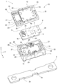
- FIG. 2 shows a state in which the lid 12 of the current sensor 1 is removed, and the lid magnetic shield 17 provided on the lid 12 and the magnetic sensor 5 provided on the substrate 4 are indicated by dotted lines.
- FIG. 3 is an exploded view of the current sensor 1 and shows a state in which the bus bar 2 is separated from the case main body 11, the substrate 4 is separated from the case main body 11, and the lid 12 is inverted.
- the current sensor 1 of the present embodiment includes a bus bar 2 through which current flows, and a case 10 that accommodates part of the bus bar 2.
- the case 10 includes a box-like case main body 11 whose upper surface is opened and a lid 12 which covers the upper surface of the case main body 11.
- the case body 11 and the lid 12 are both made of insulating synthetic resin and fixed to each other by two fixing screws 3.
- the insulating substrate 4 is fixed and accommodated in the case main body 11 by three caulking portions 13, 14 and 15.
- the caulking portions 13, 14 and 15 are portions of the case main body 11 protruding in a cylindrical shape, and a cylindrical portion is inserted through caulking holes 24 to be described later and thermally deformed from above.
- the caulking parts 13, 14 and 15 are provided at one place apart from the caulking parts 13 and 14 juxtaposed in the X direction in FIG. 2 from the caulking parts 13 and 14 to the right in the Y direction. It is comprised from the caulking part 15 provided.
- the caulking portions 13 and 14 correspond to a first fixing portion in the present invention
- the caulking portion 15 corresponds to a second fixing portion in the present invention.
- the crimped portion 15 which is the second fixed portion is provided at a position opposite to the crimped portions 13 and 14 which is the first fixed portion with the magnetic sensor 5 interposed therebetween in the Y direction.
- a main body side magnetic shield 16 is provided integrally with a resin (see FIGS. 4 to 6).
- the area surrounded by the three caulking portions 13, 14 and 15 is the fixed area 4 a.
- a region on the left side in the Y direction in FIG. 2 from the crimped portions 13 and 14 is an extended portion 4 b extending from the fixed region 4 a. That is, the extending part 4b is provided on both sides of the caulking parts 13 and 14 corresponding to the first fixing part.
- a connector 6 described later is mounted on the extending portion 4b. Therefore, the connector 6 is mounted at a position not overlapping the fixed region 4 a and the X direction which is the direction of the induction magnetic field. Further, since the crimped portions 13 and 14 are arranged in a direction parallel to the short side of the substrate 4, the extended portion 4b on which the connector 6 is mounted is easily bent.
- a magnetic sensor 5 is mounted on the back surface of the fixed area 4 a of the substrate 4.
- the magnetic sensor 5 is a sensor that detects an induced magnetic field generated by the current flowing through the bus bar 2.
- the sensitivity direction of the induction magnetic field of the magnetic sensor 5 is fixed to the substrate 4 so as to be in the X direction of the XY plane indicated by the arrow S in FIG.
- the connector 6 is mounted on the surface of the extended portion 4 b of the substrate 4.
- conductive terminals (not shown) provided inside are connected to a circuit pattern (not shown) provided on the substrate 4, and are connected to the magnetic sensor 5 via the substrate 4.
- the connector 6 is connected to a connector (not shown, the same applies hereinafter) of another device, and the signal of the magnetic sensor 5 can be output to the outside of the case 10.
- the lid 12 is provided with a metallic lid magnetic shield 17.
- the lid magnetic shield 17 is disposed inside an injection molding die (not shown, the same applies hereinafter) when molding the lid 12 and is integrally molded with the raw material resin.
- the cover 12 is provided with a connector opening 18 for exposing the connector 6 to the outside.
- two lid side stoppers 19 are provided in the vicinity of the connector opening 18 on the back surface side of the lid portion 12. Further, on the outer wall surrounding the periphery on the back surface side of the lid 12, Y-direction positioning protrusions 20 for positioning in the Y direction with respect to the case main body 11 are provided at two places.
- X direction positioning recesses 21 for positioning in the X direction are provided at two places. Further, on the back surface side of the lid portion 12, the vicinity of the insertion hole 22 through which the fixing screw 3 is inserted is a lid side Z direction positioning portion 23 for positioning in the Z direction.
- the substrate 4 is a substantially rectangular insulating plate material, and caulking holes 24 through which caulking portions 13, 14 and 15 provided in the case main body 11 are inserted are formed at three places. There is.
- main body side stoppers 25 opposed to the back surface of the substrate 4 are provided at three places. Further, in FIG. 3, the caulking portions 13, 14 and 15 show a state before caulking on the substrate 4, and are cylindrical so that they can be inserted into the caulking holes 24 of the substrate 4.
- a Y-direction positioning recess 26 for positioning in the Y direction and an X-direction positioning protrusion 27 for positioning in the X direction are formed at two positions. Further, in the vicinity of the screw hole 28 into which the fixing screw 3 is screwed, a main body side Z direction positioning portion 29 for positioning in the Z direction is formed.
- the bus bar 2 is a plate-like member extending in the Y direction, and the detection portion 2a facing the magnetic sensor 5 is formed to have a narrower width in the X direction than other portions. Further, a notch 2 b is formed on one side of the bus bar 2. When the bus bar 2 is integrally formed on the case main body 11, the notch portion 2b is used to position with the positioning convex portion (not shown) of the injection molding die. This prevents the bus bar 2 from being attached to the case body 11 in the opposite direction.
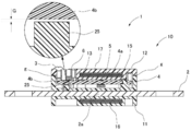
- FIG. 4 is a cross-sectional view taken along line IV-IV of FIG. 1 at the center position of the current sensor 1 in the X direction.
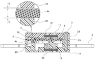
- FIG. 5 is a cross-sectional view taken along the line VV, in which a portion closer to the outer wall than in FIG. 4 is cut.
- the substrate 4 is positioned and fixed to the case body 11 by caulking portions 13 and 15.
- the magnetic sensor 5 is mounted on the fixing area 4 a on the back surface side of the substrate 4, and the connector 6 is mounted on the extended portion 4 b on the front surface side.
- a main body side stopper 25 is disposed on the back surface side of the extension portion 4 b of the substrate 4 so as to face each other via a gap G.
- a lid-side stopper 19 is disposed on the front surface side of the extended portion 4 b of the substrate 4 so as to face the substrate 4 with a gap G therebetween. Further, on the back surface side of the extended portion 4 b of the substrate 4, the main body side stoppers 25 are disposed to face each other via the gap G.
- the minimum value of the gap G is zero even when the stopper side and the substrate 4 are closest to each other, taking into consideration the dimensional tolerances of the lid side stopper 19, the body side stopper 25 and the substrate 4. It is set so as not to become smaller.
- the maximum value of the gap G is determined by the magnetic sensor 5 even when the extended portion 4 b is bent due to the positional relationship between the connector 6, the magnetic sensor 5, and the caulking portions 13, 14 and 15 on the substrate 4.
- the size is set so that the output does not change.
- the gap G is set to be between 0 mm and 0.1 mm.
- the lid portion 12 and the outer wall portion of the case body 11 are in contact with each other by the lid side Z direction positioning portion 23 and the body side Z direction positioning portion 29. It is positioned in the direction. In the other places, a gap g is formed between the lid 12 and the outer wall of the case body 11.
- the lid 12 and the case main body 11 are positioned in the X direction by the X direction positioning recess 21 provided in the lid 12 and the X direction positioning projection 27 provided in the case main body 11. It is done by fitting to.
- the positioning in the Y direction is performed by fitting to the Y direction positioning projection 20 provided on the lid 12 and the Y direction positioning recess 26 provided on the case main body 11.
- FIG. 6 is a perspective view of the current sensor 1 of the present embodiment as viewed from the back side.
- the main body side magnetic shield 16 is integrally formed with the case main body 11, a concave portion 30 formed by a shield pressing portion (not shown) provided on an injection molding die is formed on the back surface of the case main body 11 .
- a total of eight concave portions 30 are provided on each of four sides of the main body side magnetic shield 16 two each.
- a circular portion indicated by a dotted line on the side surface of the case body 11 is the gate position 31 of the injection molding die.
- the alternate long and short dash line extending in the Y direction at the center of the main body side magnetic shield 16 is a so-called resin weld line 32.
- the weld line 32 does not appear on the surface as a product.
- the concave portions 30 which are generated when the main body side magnetic shield 16 is supported in the injection molding die are provided at two places shifted from the weld line 32 in the X direction. As a result, even if distortion occurs in the case body 11 and a stress is generated in the weld line 32, a structure in which the crack is not easily generated from the weld line 32 is obtained.
- the current sensor 1 of the present embodiment is configured as described above, when the connector of another device is inserted into the connector 6, the connector 6 is pushed in the Z direction with respect to the substrate 4. At this time, the substrate 4 is bent downward in the Z direction with respect to the line connecting the caulking portions 13 and 14 which are the first fixing portions.
- three main body side stoppers 25 are provided on the back surface side of the extended portion 4b, so even if the extended portion 4b is bent in this way, the main body side stopper 25 bends by the distance G. After the connectors of other devices are attached, the extension 4b returns to its original position by its own elasticity, and the bending of the substrate 4 is eliminated.
- the fixed area 4a of the substrate 4 surrounded by the caulking parts 13, 14 and 15 is slightly affected by the bending of the extending part 4b, but after the connectors of other devices are attached, the fixing area 4a is extended. Since the deflection of the installation portion 4b is eliminated, the positional relationship between the magnetic sensor 5 mounted in the fixed area 4a and the detection portion 2a of the bus bar 2 is not affected.
- the caulking portions 13 and 14 are arranged in the X direction, and the arrangement direction is the same as the sensitivity direction S of the magnetic sensor 5. Therefore, the sensitivity direction S of the magnetic sensor 5 does not change even if a slight positional fluctuation occurs in the fixed area 4 a where the magnetic sensor 5 is mounted due to the influence of the connector 6. There is no substantial effect on sensitivity.
- the current sensor 1 of the present embodiment no influence is exerted on the magnetic sensor 5 due to the insertion and removal of connectors of other devices with respect to the connector 6, or even if it does not affect the magnetic sensor 5. Therefore, the accuracy of the current sensor 1 can be stably maintained.
- the distance G between the lid-side stopper 19 and the main body-side stopper 25 and the substrate 4 is preferably smaller in order to suppress the bending of the extended portion 4b, but the distance G is minimized due to the dimensional tolerance of each member. It is necessary to make it not smaller than zero even if it becomes.
- the gap G becomes negative the lid side stopper 19 or the main body side stopper 25 and the substrate 4 always abut, and the substrate 4 is put in a deformed state, so the extension portion 4b is bent and the magnetic area of the fixed area 4a This is because the position of the sensor 5 is also affected.
- the fixing portion for fixing the substrate 4 to the case main body 11 is provided with the caulking portions 13 and 14 as the first fixing portion, and the caulking portion 15 is provided as the second fixing portion.
- the fixing area 4a is formed by the three caulking portions 13, 14 and 15 as described above, the fixing area 4a has a triangular shape, so that the influence from the outside is hardly affected.
- the crimping parts 13, 14, and 15 are set to three places, it does not restrict to this, It is good also as four or more places.
- the distance G between the substrate 4 and the lid side stopper 19 and the distance G between the substrate 4 and the main body side stopper 25 have the same size, but the size is not limited to this. May be
- the case 10 is formed of two members, the lid 12 and the case main body 11, and the thickness of the lid 12 is thinner than that of the case main body 11.
- the shape is not limited to the above embodiment.
- the thickness of the lid 12 may be formed thicker than the thickness of the case body 11.
- the fixing portions for fixing the substrate 4 and the case main body 11 are the caulking portions 13, 14 and 15, but the invention is not limited thereto.
- other fixing means such as screwing or riveting may be used.
- each stopper is formed by an elliptical protrusion, but the present invention is not limited to this, and any shape such as a cylindrical shape or a prismatic shape can be used as long as it can minimize the bending of the substrate 4. Good.
- the lid magnetic shield 17 and the main magnetic shield 16 are fixed to the lid 12 and the case main body 11 by integral molding.
- the present invention is not limited thereto. It may be crimped or may be fixed by other fixing method.
Landscapes
- Physics & Mathematics (AREA)
- General Physics & Mathematics (AREA)
- Measuring Instrument Details And Bridges, And Automatic Balancing Devices (AREA)
Abstract
出力をコネクタを介して外部に出力する電流センサであって、コネクタを挿抜してもセンサの精度に影響を与えることのない電流センサ1は、バスバ2とその一部を収容するケース10を備える。ケース10は、上面が開放された箱状のケース本体11と、その上面を覆う蓋部12とからなる。ケース本体11には基板4が3箇所のカシメ部13~15で固定される。基板4は、3箇所のカシメ部13~15で囲まれる領域が固定領域4aであり、カシメ部13,14から突出する領域が延設部4bである。蓋部12は、蓋側ストッパ19が2個設けられる。ケース本体11の内側には、本体側ストッパ25が3箇所に設けられる。コネクタ6に他の機器のコネクタを挿抜する場合、延設部4bに撓みが生じるが、本体側ストッパ25及び蓋側ストッパ19により撓みが抑えられる。
Description
本発明は、被測定電流によって生じる磁界に基づいて電流値を算出する電流センサに関する。
電流によって生じる磁界に基づいて電流値を算出する電流センサとしては、特許文献1に記載のものが知られている。特許文献1に記載の電流センサは、被測定電流が流れる導体と、被測定電流が発生する誘導磁界を測定する磁気センサとを、蓋を有するケースに収納するものであって、ケースの底部及び蓋部に一体成形により固定された磁気シールドを備えている。
特許文献1の電流センサでは、磁気センサの信号は、基板に実装されたコネクタをケースの側壁に設けられた開口部で露出させ、外部からコネクタを接続することで、外部への出力が可能となっている。
特許文献1に記載の電流センサでは、基板の端部にコネクタが設けられており、接続される相手側のコネクタの着脱方向は、基板の面に対して平行となるように形成されている。このため、相手側のコネクタを挿抜する場合であっても基板の面と垂直方向にはさほど力はかからない。
一方で、電流センサにおいては、接続される機器の位置関係等の理由により、基板の面に対して垂直方向に向けてコネクタを実装する場合がある。この場合、基板側のコネクタに対して相手側のコネクタを挿抜する際に、基板の面と垂直方向に直接力が加わるため、基板に歪みが生じるおそれがある。
このように基板に歪みが生じると、基板に実装された磁気センサと導体とのクリアランス、及び磁気センサと磁気シールドとのクリアランスに変動が生じて磁気センサの精度が低下するおそれがある。
本発明は、上記課題を解決するために、電流センサでセンサの出力をコネクタを介して外部に出力するものにおいて、コネクタを挿抜する場合であってもセンサの精度に影響を与えることのない電流センサを提供することを目的とする。
上記目的を達成するために、本発明の電流センサは、電流が流れるバスバと、前記バスバに流れる電流によって生じる誘導磁界を検出する磁気センサと、前記磁気センサが実装される絶縁性の基板と、前記基板に実装され、前記基板を介して前記磁気センサに接続され、前記磁気センサからの信号を外部に出力可能なコネクタと、前記バスバの一部と前記基板とを収容し、ケース本体及び蓋部を有するケースとを備えた電流センサであって、前記基板は前記ケース本体に対して複数の固定部で固定され、前記磁気センサは前記複数の固定部で囲まれる固定領域内に設けられ、前記コネクタは、前記固定領域から延びる延設部に設けられ、前記ケース本体及び前記蓋部に、前記延設部の表面及び裏面に対して間隔を介して対向するストッパを備えていることを特徴とする電流センサ。
本発明の電流センサによれば、磁気センサは、複数の固定部で囲まれる固定領域内に設けられ、コネクタは固定領域から延びる延設部に設けられている。また、延設部の表面及び裏面には、間隔を介して対向するストッパが設けられている。従って、コネクタに対して相手側のコネクタを挿抜した場合、延設部はストッパとの間隔のみ板厚方向に撓むことができ、固定領域は複数の固定部で囲まれているため撓みは抑制される。このため、バスバと磁気センサとの位置関係に変動が生じないので、電流センサの精度を確保することができる。
本発明の電流センサにおいては、前記磁気センサは、XY平面において前記誘導磁界の感度方向がX方向となるように配置され、前記複数の固定部のうち、前記磁気センサと前記コネクタとの間に配置される第1固定部が、X方向に向けて2箇所に配置されており、前記コネクタが設けられる前記延設部は、前記第1固定部を挟んで前記固定領域と隣り合うことが好ましい。
本発明の電流センサによれば、磁気センサとコネクタとの間に、第1固定部としてX方向に2箇所に配置されている。従って、コネクタの挿抜が行われた際にコネクタが固定されている延設部に撓みが生じた場合、X方向の撓みは2箇所の第1固定部によって抑制される。このため、固定領域においてもX方向の撓みが抑制され、磁気センサの感度方向には影響が及ばないため、電流センサの精度を確保することができる。
また、本発明の電流センサにおいては、前記固定部は、前記磁気センサを挟んで前記第1固定部とはY方向の反対位置に1箇所に形成された第2固定部を備えていることが好ましい。当該構成によれば、固定領域はX方向の2箇所の固定部と、Y方向の1箇所の固定部に囲まれて三角形となるので、延設部に撓みが生じた場合でも固定領域内の撓みは最小限に抑制される。
また、本発明の電流センサにおいて、前記蓋部に磁気シールドが設けられているときは、磁気シールドと磁気センサとの位置関係に変動が生じないことになるため、磁気シールドを有する電流センサの精度を確保することができる。
本発明によれば、電流センサでセンサの出力をコネクタを介して外部に出力するものにおいて、コネクタを挿抜する場合であってもセンサの精度に影響を与えることのない電流センサを提供することができる。
次に、本発明の実施形態の一例である電流センサについて、図1~図6を参照して説明する。本実施形態の電流センサ1は、例えばハイブリッド車両や電気自動車に用いられる制御装置等の大電流を必要とする機器に用いることができるセンサである。
図1は、本発明の実施形態の一例である電流センサ1の外観を示す斜視図である。図2は、電流センサ1の蓋部12を取り外した状態であり、蓋部12に設けられた蓋部磁気シールド17と、基板4に設けられた磁気センサ5を点線で示している。図3は、電流センサ1の分解図であり、バスバ2をケース本体11から分離し、基板4をケース本体11から分離し、蓋部12を反転させた状態を示している。
図1に示すように、本実施形態の電流センサ1は、内部に電流が流れるバスバ2と、バスバ2の一部を収容するケース10を備えている。図2に示すように、ケース10は、上面が開放された箱状のケース本体11と、ケース本体11の上面を覆う蓋部12とからなる。このケース本体11及び蓋部12は、共に絶縁性の合成樹脂で形成されており、2本の固定ビス3で互いに固定されている。
また、図2に示すように、ケース本体11には絶縁性の基板4が3箇所のカシメ部13,14,15で固定されて収容されている。このカシメ部13,14,15は、ケース本体11の一部を円柱状に突出させ、後述するカシメ穴24に円柱状部分を挿通させて上方から加熱変形させたものであり、本発明における複数の固定部に相当する。
本実施形態では、カシメ部13,14,15は、図2においてX方向に向けて併設されたカシメ部13及び14と、これらのカシメ部13,14からY方向の右側に離れて1箇所に設けられたカシメ部15とから構成される。本実施形態では、カシメ部13,14が本発明における第1固定部に相当し、カシメ部15が本発明における第2固定部に相当する。
この第2固定部であるカシメ部15は、磁気センサ5を挟んで第1固定部であるカシメ部13,14とはY方向の反対位置に設けられている。なお、ケース本体11の内部には、本体側磁気シールド16が樹脂と一体成形されて設けられている(図4~図6参照)。
本実施形態においては、基板4の領域のうち、3箇所のカシメ部13,14,15で囲まれる領域が固定領域4aとなっている。また、基板4のうち、カシメ部13,14から、図2においてY方向の左側の領域が、固定領域4aから延びる延設部4bとなっている。即ち、第1固定部に相当するカシメ部13,14を挟んで延設部4bが設けられる。延設部4bには、後述するコネクタ6が実装される。よって、コネクタ6は、固定領域4aと、誘導磁界の方向であるX方向と重ならない位置に実装される。また、カシメ部13,14は、基板4の短辺と平行な方向に並んでいるので、コネクタ6が実装される延設部4bは、曲がりやすくなっている。
基板4の固定領域4aの裏面には磁気センサ5が実装されている。磁気センサ5は、バスバ2に流れる電流によって生じる誘導磁界を検出するセンサである。本実施形態においては、磁気センサ5の誘導磁界の感度方向が、図2における矢印Sで示すXY平面のX方向となるように基板4に固定されている。
基板4の延設部4bの表面には、コネクタ6が実装されている。コネクタ6は、内部に設けられた導電性の端子(図示省略)が、基板4に設けられた回路パターン(図示省略)に接続され、基板4を介して磁気センサ5に接続されている。また、コネクタ6は、他の機器のコネクタ(図示省略、以下同様。)に接続されて、磁気センサ5の信号をケース10の外部に出力可能となっている。
図2に示すように、蓋部12には金属製の蓋部磁気シールド17が設けられている。本実施形態では、蓋部磁気シールド17は、蓋部12を成形する際に、射出成形金型(図示省略、以下同様。)の内部に配置されて原料の樹脂と共に一体に成形されている。また、蓋部12には、コネクタ6を外部に露出させるコネクタ開口18が設けられている。
図3に示すように、蓋部12は、裏面側のコネクタ開口18の近傍に、蓋側ストッパ19(ストッパ)が2個設けられている。また、蓋部12の裏面側の周囲を囲む外壁には、ケース本体11に対してY方向の位置決めを行うY方向位置決め突起20が2箇所に設けられている。
同様に、外壁のX方向には、X方向の位置決めを行うX方向位置決め凹部21が2箇所に設けられている。また、蓋部12の裏面側において、固定ビス3が挿通される挿通穴22の近傍は、Z方向の位置決めを行う蓋側Z方向位置決め部23となっている。
図3に示すように、基板4は、略四角形状の絶縁性の板材であり、ケース本体11に設けられたカシメ部13,14,15が挿通されるカシメ穴24が3箇所に形成されている。
ケース本体11の内側には、基板4の裏面に対向する本体側ストッパ25(ストッパ)が3箇所に設けられている。また、図3においては、カシメ部13,14,15は基板4にかしめる前の状態を示しており、基板4のカシメ穴24に挿通可能なように円柱状となっている。
ケース本体11の外壁部分には、Y方向の位置決めを行うY方向位置決め凹部26と、X方向の位置決めを行うX方向位置決め突起27がそれぞれ2箇所に形成されている。また、固定ビス3がネジ止めされるネジ穴28の近傍には、Z方向の位置決めを行う本体側Z方向位置決め部29が形成されている。
バスバ2は、Y方向に延びる板状の部材であり、磁気センサ5に対向する被検出部2aは他の部分に比べてX方向の幅が狭くなるように形成されている。また、バスバ2の一方の側辺には切り欠き部2bが形成されている。この切り欠き部2bは、バスバ2をケース本体11に一体成形する際に、射出成形金型の位置決め凸部(図示省略)で位置決めするためのものである。これにより、バスバ2がケース本体11に対して逆方向に取り付けられることが防止される。
次に、図4及び図5を参照して、本実施形態の電流センサ1の内部構造について説明する。図4は、電流センサ1のX方向の中心位置における図1のIV-IV線断面図である。図5は、図4よりも手前側で外壁に近い箇所を切断したV-V線断面図である。
図4に示すように、基板4は、ケース本体11に対してカシメ部13及び15で位置決め固定されている。基板4の裏面側には固定領域4aに磁気センサ5が実装され、表面側の延設部4bにはコネクタ6が実装されている。基板4の延設部4bの裏面側には、本体側ストッパ25が間隔Gを介して対向するように配置されている。
図5に示すように、基板4の延設部4bの表面側には、蓋側ストッパ19が間隔Gを介して基板4に対向するように配置されている。また、基板4の延設部4bの裏面側には、本体側ストッパ25が間隔Gを介して対向するように配置されている。
本実施形態においては、この間隔Gの最小値は、蓋側ストッパ19、本体側ストッパ25及び基板4のそれぞれの寸法公差を考慮し、ストッパ側と基板4が最も接近する場合であってもゼロより小さくなることがないように設定されている。
また、間隔Gの最大値は、基板4上におけるコネクタ6、磁気センサ5及びカシメ部13,14,15の位置関係から、延設部4bを撓ませた場合であっても、磁気センサ5の出力に変化が出ない大きさに設定している。本実施形態では、間隔Gは、0mm~0.1mmの間となるように設定されている。
また、蓋部12とケース本体11の外壁部は、図5に示すように、蓋側Z方向位置決め部23と本体側Z方向位置決め部29が当接して蓋部12とケース本体11とがZ方向に位置決めされている。その他の箇所においては、蓋部12とケース本体11の外壁部の間には間隔gが形成されている。
また、図1に示すように、蓋部12とケース本体11とは、X方向の位置決めは、蓋部12に設けられたX方向位置決め凹部21とケース本体11に設けられたX方向位置決め突起27に嵌合することよって行われている。同様に、Y方向の位置決めは、蓋部12に設けられたY方向位置決め突起20と、ケース本体11に設けられたY方向位置決め凹部26に嵌合することよって行われている。
図6は、本実施形態の電流センサ1を裏面側から見た斜視図である。ケース本体11の裏面には、本体側磁気シールド16をケース本体11と一体成形する際に、射出成形金型に設けられたシールド押さえ部(図示省略)によって形成された凹部30が形成されている。この凹部30は、本実施形態では、本体側磁気シールド16の4辺に2個ずつ、合計8個設けられている。
ここで、図6において、ケース本体11の側面において点線で示す円形の箇所は、射出成形金型のゲート位置31である。また、図6において、本体側磁気シールド16の中央にY方向に延びている一点鎖線は、いわゆる樹脂のウエルドライン32である。なお、このウエルドライン32は、製品としては表面に表れていない。
本実施形態においては、本体側磁気シールド16を射出成形金型内で支持する際に生じる凹部30を、このウエルドライン32からX方向にずらして2箇所に設けている。これにより、ケース本体11に歪みが生じてウエルドライン32に応力が発生した場合であっても、ウエルドライン32から亀裂が生じにくい構造となっている。
本実施形態の電流センサ1は、上記構成となっているので、コネクタ6に他の機器のコネクタが差し込まれた場合、コネクタ6が基板4に対してZ方向に押されることになる。このとき、基板4は、延設部4bが第1固定部であるカシメ部13及び14を結ぶ線を境としてZ方向の下方に撓む。
延設部4bの裏面側には、図3に示すように、3個の本体側ストッパ25が設けられているので、このように延設部4bが撓んだ場合であっても本体側ストッパ25によって間隔Gの分だけ撓む。他の機器のコネクタが装着された後は、延設部4bは自己の弾性により元の位置に戻り、基板4の撓みは解消される。
このとき、カシメ部13,14,15によって囲まれている基板4の固定領域4aは、延設部4bの撓みによってわずかに影響を受けるが、他の機器のコネクタが装着された後は、延設部4bの撓みが解消するので、固定領域4aに実装されている磁気センサ5とバスバ2の被検出部2aとの位置関係には影響が残らない。
また、カシメ部13及び14は、X方向に配列されており、この配列方向は磁気センサ5の感度方向Sと同一となっている。よって、仮にコネクタ6に生じる影響によって磁気センサ5が実装されている固定領域4aに若干の位置変動が生じた場合であっても、磁気センサ5の感度方向Sは変化しないので、磁気センサ5の感度には実質的な影響はない。
このように、本実施形態の電流センサ1によれば、コネクタ6に対する他の機器のコネクタの挿抜による磁気センサ5への影響は生じないか、生じた場合でも実質的に影響を与えるものではないため、安定して電流センサ1の精度を保つことができる。
上記実施形態において、蓋側ストッパ19及び本体側ストッパ25と基板4との間隔Gは、延設部4bの撓みを抑えるために小さい方がよいが、各部材の寸法公差で間隔Gが最小になった場合でもゼロより小さくならないようにする必要がある。間隔Gがマイナスになると、蓋側ストッパ19又は本体側ストッパ25と基板4が常に当接し、基板4を変形状態とすることになるため、延設部4bに撓みが生じて固定領域4aの磁気センサ5の位置にも影響が及ぶためである。
また、本実施形態においては、基板4をケース本体11に固定する固定部を、第1固定部としてカシメ部13及び14を設け、第2固定部としてカシメ部15を設けている。このように3個のカシメ部13,14,15で固定領域4aを形成する場合、固定領域4aは三角形となるため、外部からの影響を受けにくくなる。
なお、上記実施形態においては、カシメ部13,14,15を3箇所に設定しているが、これに限らず、4箇所以上としてもよい。また、上記実施形態では、基板4と蓋側ストッパ19との間隔Gと、基板4と本体側ストッパ25との間隔Gを共通の大きさとしているが、これに限らず、それぞれ寸法を設定してもよい。
また、ケース10は、蓋部12及びケース本体11の2部材で形成しており、蓋部12がケース本体11よりも厚さが薄く形成されているが、上記実施形態の形状に限らず、蓋部12の厚さをケース本体11の厚さよりも厚く形成してもよい。
また、上記実施形態では、基板4とケース本体11とを固定する固定部をカシメ部13,14,15としているが、これに限らず、カシメ穴24をケース本体11に設けた円柱部に圧入するようにしてもよく、ビス止めやリベット止め等の他の固定手段を用いてもよい。
また、上記実施形態では、各ストッパは、楕円状の突起により形成しているが、これに限らず、円柱状や角柱状等、基板4の撓みを最小限に抑えることができる形状であればよい。
また、上記実施形態では、蓋部磁気シールド17及び本体側磁気シールド16を、蓋部12及びケース本体11に一体成形で固定しているが、これに限らず、基板4と同様にカシメ部によりかしめ止めしてもよく、他の固定方法で固定してもよい。
1…電流センサ
2…バスバ
4…基板
4a…固定領域
4b…延設部
5…磁気センサ
6…コネクタ
10…ケース
11…ケース本体
12…蓋部
13~15…カシメ部
16…本体側磁気シールド
17…蓋部磁気シールド
18…コネクタ開口
19…蓋側ストッパ
25…本体側ストッパ
2…バスバ
4…基板
4a…固定領域
4b…延設部
5…磁気センサ
6…コネクタ
10…ケース
11…ケース本体
12…蓋部
13~15…カシメ部
16…本体側磁気シールド
17…蓋部磁気シールド
18…コネクタ開口
19…蓋側ストッパ
25…本体側ストッパ
Claims (4)
- 電流が流れるバスバと、
前記バスバに流れる電流によって生じる誘導磁界を検出する磁気センサと、
前記磁気センサが実装される絶縁性の基板と、
前記基板に実装され、前記基板を介して前記磁気センサに接続され、前記磁気センサからの信号を外部に出力可能なコネクタと、
前記バスバの一部と前記基板とを収容し、ケース本体及び蓋部を有するケースとを備えた電流センサであって、
前記基板は前記ケース本体に対して複数の固定部で固定され、前記磁気センサは前記複数の固定部で囲まれる固定領域内に設けられ、
前記コネクタは、前記固定領域から延びる延設部に設けられ、
前記ケース本体及び前記蓋部に、前記延設部の表面及び裏面に対して間隔を介して対向するストッパを備えていることを特徴とする電流センサ。 - 前記磁気センサは、XY平面において前記誘導磁界の感度方向がX方向となるように配置され、
前記複数の固定部のうち、前記磁気センサと前記コネクタとの間に配置される第1固定部が、X方向に向けて2箇所に配置されており、
前記コネクタが設けられる前記延設部は、前記第1固定部を挟んで前記固定領域と隣り合うことを特徴とする請求項1に記載の電流センサ。 - 前記固定部は、前記磁気センサを挟んで前記第1固定部とはY方向の反対位置に1箇所に形成された第2固定部を備えていることを特徴とする請求項2に記載の電流センサ。
- 前記蓋部に磁気シールドが設けられていることを特徴とする請求項1から3のいずれか一項に記載の電流センサ。
Priority Applications (4)
| Application Number | Priority Date | Filing Date | Title |
|---|---|---|---|
| EP18888921.6A EP3726228B1 (en) | 2017-12-13 | 2018-12-11 | Current sensor |
| JP2019559677A JP6890679B2 (ja) | 2017-12-13 | 2018-12-11 | 電流センサ |
| CN201880079733.5A CN111465861B (zh) | 2017-12-13 | 2018-12-11 | 电流传感器 |
| US16/899,322 US11287451B2 (en) | 2017-12-13 | 2020-06-11 | Current sensor |
Applications Claiming Priority (2)
| Application Number | Priority Date | Filing Date | Title |
|---|---|---|---|
| JP2017238494 | 2017-12-13 | ||
| JP2017-238494 | 2017-12-13 |
Related Child Applications (1)
| Application Number | Title | Priority Date | Filing Date |
|---|---|---|---|
| US16/899,322 Continuation US11287451B2 (en) | 2017-12-13 | 2020-06-11 | Current sensor |
Publications (1)
| Publication Number | Publication Date |
|---|---|
| WO2019117174A1 true WO2019117174A1 (ja) | 2019-06-20 |
Family
ID=66819355
Family Applications (1)
| Application Number | Title | Priority Date | Filing Date |
|---|---|---|---|
| PCT/JP2018/045575 Ceased WO2019117174A1 (ja) | 2017-12-13 | 2018-12-11 | 電流センサ |
Country Status (5)
| Country | Link |
|---|---|
| US (1) | US11287451B2 (ja) |
| EP (1) | EP3726228B1 (ja) |
| JP (1) | JP6890679B2 (ja) |
| CN (1) | CN111465861B (ja) |
| WO (1) | WO2019117174A1 (ja) |
Cited By (3)
| Publication number | Priority date | Publication date | Assignee | Title |
|---|---|---|---|---|
| JPWO2024089975A1 (ja) * | 2022-10-24 | 2024-05-02 | ||
| WO2024157806A1 (ja) * | 2023-01-27 | 2024-08-02 | 株式会社デンソー | 電流センサ |
| CN118731448A (zh) * | 2024-09-04 | 2024-10-01 | 宁波中车时代传感技术有限公司 | 一种igbt集成一体化电流传感器 |
Families Citing this family (6)
| Publication number | Priority date | Publication date | Assignee | Title |
|---|---|---|---|---|
| JP7003620B2 (ja) * | 2017-12-14 | 2022-01-20 | 日立金属株式会社 | 電流センサ |
| JP7087512B2 (ja) * | 2018-03-20 | 2022-06-21 | 株式会社デンソー | 電流センサ |
| US12529380B2 (en) | 2020-11-09 | 2026-01-20 | Pierburg Pump Technology Gmbh | Electric coolant pump |
| FR3145212B1 (fr) * | 2023-01-20 | 2026-02-27 | Electricfil Automotive | Ensemble de détection de courant et bloc moteur comprenant un tel ensemble de détection. |
| US12283805B2 (en) * | 2023-03-30 | 2025-04-22 | BorgWarner US Technologies LLC | Bus bar assembly |
| US12598708B2 (en) * | 2023-11-30 | 2026-04-07 | Caterpillar Inc. | Detachable sensor assembly for an elongate conductor |
Citations (5)
| Publication number | Priority date | Publication date | Assignee | Title |
|---|---|---|---|---|
| JPH0567072U (ja) * | 1992-02-21 | 1993-09-03 | 矢崎総業株式会社 | コネクタ基板の固定構造 |
| JP2010230329A (ja) * | 2009-03-25 | 2010-10-14 | Panasonic Electric Works Co Ltd | 基板固定構造および物理量センサ |
| JP2013113631A (ja) * | 2011-11-25 | 2013-06-10 | Yazaki Corp | 電流検出装置 |
| JP2015145839A (ja) * | 2014-02-03 | 2015-08-13 | 株式会社フジクラ | 電流検出装置 |
| WO2018012034A1 (ja) * | 2016-07-15 | 2018-01-18 | アルプス電気株式会社 | 電流センサ |
Family Cites Families (14)
| Publication number | Priority date | Publication date | Assignee | Title |
|---|---|---|---|---|
| CA2195830C (en) * | 1996-01-31 | 2000-05-16 | Kouichi Uezono | Connector fixing construction |
| JP5414333B2 (ja) | 2009-04-09 | 2014-02-12 | 矢崎総業株式会社 | 電流検出装置の組付け構造 |
| JP2011064648A (ja) * | 2009-09-18 | 2011-03-31 | Tokai Rika Co Ltd | 電流センサ |
| JP5872758B2 (ja) * | 2010-04-28 | 2016-03-01 | 矢崎総業株式会社 | 電流検出装置 |
| JP2013015431A (ja) * | 2011-07-05 | 2013-01-24 | Sumitomo Wiring Syst Ltd | 電流検出装置 |
| EP2546660A1 (en) * | 2011-07-13 | 2013-01-16 | LEM Intellectual Property SA | Electrical current sensor with grounded magnetic core |
| JP5817508B2 (ja) * | 2011-12-22 | 2015-11-18 | 住友電装株式会社 | 電流検出装置 |
| DE202012103071U1 (de) * | 2012-08-14 | 2012-09-24 | Rauschert Heinersdorf-Pressig Gmbh | Messeinrichtung für eine kontaktlose Strommessung |
| JP6372969B2 (ja) * | 2012-12-03 | 2018-08-15 | 矢崎総業株式会社 | 電流センサ |
| US10247759B2 (en) * | 2013-09-05 | 2019-04-02 | Asahi Kasei Microdevices Corporation | Current sensor |
| JP2015145838A (ja) * | 2014-02-03 | 2015-08-13 | 株式会社フジクラ | 電流検出装置及びバスバー付き電流検出装置 |
| JP6570811B2 (ja) * | 2014-04-10 | 2019-09-04 | 日立金属株式会社 | コネクタ |
| JP6477089B2 (ja) * | 2014-05-23 | 2019-03-06 | 株式会社デンソー | 電流センサ付バスバーモジュール |
| JP6076952B2 (ja) * | 2014-11-21 | 2017-02-08 | 矢崎総業株式会社 | 基板用端子及び端子付き基板 |
-
2018
- 2018-12-11 JP JP2019559677A patent/JP6890679B2/ja active Active
- 2018-12-11 WO PCT/JP2018/045575 patent/WO2019117174A1/ja not_active Ceased
- 2018-12-11 EP EP18888921.6A patent/EP3726228B1/en active Active
- 2018-12-11 CN CN201880079733.5A patent/CN111465861B/zh active Active
-
2020
- 2020-06-11 US US16/899,322 patent/US11287451B2/en active Active
Patent Citations (5)
| Publication number | Priority date | Publication date | Assignee | Title |
|---|---|---|---|---|
| JPH0567072U (ja) * | 1992-02-21 | 1993-09-03 | 矢崎総業株式会社 | コネクタ基板の固定構造 |
| JP2010230329A (ja) * | 2009-03-25 | 2010-10-14 | Panasonic Electric Works Co Ltd | 基板固定構造および物理量センサ |
| JP2013113631A (ja) * | 2011-11-25 | 2013-06-10 | Yazaki Corp | 電流検出装置 |
| JP2015145839A (ja) * | 2014-02-03 | 2015-08-13 | 株式会社フジクラ | 電流検出装置 |
| WO2018012034A1 (ja) * | 2016-07-15 | 2018-01-18 | アルプス電気株式会社 | 電流センサ |
Non-Patent Citations (1)
| Title |
|---|
| See also references of EP3726228A4 * |
Cited By (4)
| Publication number | Priority date | Publication date | Assignee | Title |
|---|---|---|---|---|
| JPWO2024089975A1 (ja) * | 2022-10-24 | 2024-05-02 | ||
| WO2024157806A1 (ja) * | 2023-01-27 | 2024-08-02 | 株式会社デンソー | 電流センサ |
| CN118731448A (zh) * | 2024-09-04 | 2024-10-01 | 宁波中车时代传感技术有限公司 | 一种igbt集成一体化电流传感器 |
| CN118731448B (zh) * | 2024-09-04 | 2024-11-15 | 宁波中车时代传感技术有限公司 | 一种igbt集成一体化电流传感器 |
Also Published As
| Publication number | Publication date |
|---|---|
| US11287451B2 (en) | 2022-03-29 |
| EP3726228A1 (en) | 2020-10-21 |
| US20200300896A1 (en) | 2020-09-24 |
| JPWO2019117174A1 (ja) | 2020-10-01 |
| EP3726228A4 (en) | 2021-08-25 |
| CN111465861B (zh) | 2022-12-30 |
| EP3726228B1 (en) | 2023-06-07 |
| CN111465861A (zh) | 2020-07-28 |
| JP6890679B2 (ja) | 2021-06-18 |
Similar Documents
| Publication | Publication Date | Title |
|---|---|---|
| WO2019117174A1 (ja) | 電流センサ | |
| CN111465862B (zh) | 电流传感器 | |
| US10566741B2 (en) | Shielded connector | |
| JP6441112B2 (ja) | 電子部品ユニット、及び、ワイヤハーネス | |
| US9255976B2 (en) | Current detection device | |
| US10574043B2 (en) | Electrical connection box | |
| WO2011129338A1 (ja) | 電子部品 | |
| EP3598583B1 (en) | Electronic device having fixed electric conductive plate and flexible electric conductive plate | |
| JP2013015425A (ja) | 電流検出装置 | |
| JP2013130518A (ja) | 電流検出装置 | |
| CN108879533A (zh) | 电接线箱 | |
| JP2009258048A (ja) | 電流センサ | |
| JP6064117B2 (ja) | 電流センサ | |
| JP2014010012A (ja) | 電流センサ | |
| JP4763576B2 (ja) | カードエッジ型コネクタ | |
| JP2012247241A (ja) | 電流検出装置 | |
| JP2016065736A (ja) | 電流センサ | |
| JP2013044671A (ja) | 電流検出装置 | |
| JP5978511B2 (ja) | カメラ装置 | |
| WO2021157400A1 (ja) | 電気接続箱 | |
| JP7512992B2 (ja) | コネクタ | |
| US20250044165A1 (en) | Thermistor | |
| US20240055795A1 (en) | Electrical device, device connection part for the electrical device, and method for manufacturing an electrical device | |
| JP2018092774A (ja) | 電子部品及び撮像装置 | |
| JP2025042899A (ja) | 電流検出器 |
Legal Events
| Date | Code | Title | Description |
|---|---|---|---|
| 121 | Ep: the epo has been informed by wipo that ep was designated in this application |
Ref document number: 18888921 Country of ref document: EP Kind code of ref document: A1 |
|
| ENP | Entry into the national phase |
Ref document number: 2019559677 Country of ref document: JP Kind code of ref document: A |
|
| NENP | Non-entry into the national phase |
Ref country code: DE |
|
| ENP | Entry into the national phase |
Ref document number: 2018888921 Country of ref document: EP Effective date: 20200713 |