WO2019124106A1 - 撮像装置、および撮像方法、並びに撮像素子 - Google Patents
撮像装置、および撮像方法、並びに撮像素子 Download PDFInfo
- Publication number
- WO2019124106A1 WO2019124106A1 PCT/JP2018/045019 JP2018045019W WO2019124106A1 WO 2019124106 A1 WO2019124106 A1 WO 2019124106A1 JP 2018045019 W JP2018045019 W JP 2018045019W WO 2019124106 A1 WO2019124106 A1 WO 2019124106A1
- Authority
- WO
- WIPO (PCT)
- Prior art keywords
- imaging device
- regions
- mask
- incident light
- solid
- Prior art date
- Legal status (The legal status is an assumption and is not a legal conclusion. Google has not performed a legal analysis and makes no representation as to the accuracy of the status listed.)
- Ceased
Links
Images


Classifications
-
- G—PHYSICS
- G02—OPTICS
- G02B—OPTICAL ELEMENTS, SYSTEMS OR APPARATUS
- G02B5/00—Optical elements other than lenses
- G02B5/18—Diffraction gratings
- G02B5/1842—Gratings for image generation
-
- G—PHYSICS
- G02—OPTICS
- G02B—OPTICAL ELEMENTS, SYSTEMS OR APPARATUS
- G02B27/00—Optical systems or apparatus not provided for by any of the groups G02B1/00 - G02B26/00, G02B30/00
- G02B27/42—Diffraction optics, i.e. systems including a diffractive element being designed for providing a diffractive effect
- G02B27/4205—Diffraction optics, i.e. systems including a diffractive element being designed for providing a diffractive effect having a diffractive optical element [DOE] contributing to image formation, e.g. whereby modulation transfer function MTF or optical aberrations are relevant
-
- G—PHYSICS
- G02—OPTICS
- G02B—OPTICAL ELEMENTS, SYSTEMS OR APPARATUS
- G02B27/00—Optical systems or apparatus not provided for by any of the groups G02B1/00 - G02B26/00, G02B30/00
- G02B27/42—Diffraction optics, i.e. systems including a diffractive element being designed for providing a diffractive effect
- G02B27/46—Systems using spatial filters
-
- G—PHYSICS
- G02—OPTICS
- G02B—OPTICAL ELEMENTS, SYSTEMS OR APPARATUS
- G02B5/00—Optical elements other than lenses
- G02B5/18—Diffraction gratings
- G02B5/1866—Transmission gratings characterised by their structure, e.g. step profile, contours of substrate or grooves, pitch variations, materials
-
- G—PHYSICS
- G03—PHOTOGRAPHY; CINEMATOGRAPHY; ANALOGOUS TECHNIQUES USING WAVES OTHER THAN OPTICAL WAVES; ELECTROGRAPHY; HOLOGRAPHY
- G03B—APPARATUS OR ARRANGEMENTS FOR TAKING PHOTOGRAPHS OR FOR PROJECTING OR VIEWING THEM; APPARATUS OR ARRANGEMENTS EMPLOYING ANALOGOUS TECHNIQUES USING WAVES OTHER THAN OPTICAL WAVES; ACCESSORIES THEREFOR
- G03B11/00—Filters or other obturators specially adapted for photographic purposes
-
- H—ELECTRICITY
- H04—ELECTRIC COMMUNICATION TECHNIQUE
- H04N—PICTORIAL COMMUNICATION, e.g. TELEVISION
- H04N23/00—Cameras or camera modules comprising electronic image sensors; Control thereof
- H04N23/95—Computational photography systems, e.g. light-field imaging systems
- H04N23/955—Computational photography systems, e.g. light-field imaging systems for lensless imaging
-
- H—ELECTRICITY
- H04—ELECTRIC COMMUNICATION TECHNIQUE
- H04N—PICTORIAL COMMUNICATION, e.g. TELEVISION
- H04N23/00—Cameras or camera modules comprising electronic image sensors; Control thereof
- H04N23/95—Computational photography systems, e.g. light-field imaging systems
- H04N23/957—Light-field or plenoptic cameras or camera modules
-
- G—PHYSICS
- G02—OPTICS
- G02B—OPTICAL ELEMENTS, SYSTEMS OR APPARATUS
- G02B5/00—Optical elements other than lenses
- G02B5/18—Diffraction gratings
- G02B2005/1804—Transmission gratings
Definitions
- the present disclosure relates to an imaging device, an imaging method, and an imaging device, and in particular, a lensless imaging device can capture a two-dimensional image with high spatial resolution as a final image even when acquiring a wide range of wavelengths simultaneously.
- the present invention relates to an imaging device, an imaging method, and an imaging device.
- the lensless imaging apparatus captures images using a mechanism that modulates light such as a pattern aperture or a diffraction grating with a two-dimensional image sensor without using a lens that has been used in a conventional two-dimensional image capturing system.
- the image processing apparatus performs signal processing on the pixel signals of (1) to reconstruct a two-dimensional final image, and realizes downsizing, weight reduction, cost reduction, non-planarization, and the like of the imaging apparatus.
- Non-Patent Document 1 a method of controlling light incident on an imaging surface of a two-dimensional image sensor by a Fresnel structure mask opening and reconstructing a final image by Fourier transform-based signal processing.
- Patent Documents 1 and 2 and Non-Patent Document 1 all claim that they are scalable methods for the wavelength of the incident light as the input.
- the lensless imaging apparatus is a technology that can be applied to imaging of X-rays and ⁇ -rays, and has been used for astronomical image observation. In theory, it is also applicable to imaging of millimeter waves and terahertz waves.
- the pattern, shape, etc. of the aperture that modulates light in each method need to be optimized for the target wavelength. This is because diffraction is a phenomenon that depends on the wavelength of incident light.
- the amount of blurring due to diffraction may increase unless the distance between the pattern mask and the image sensor or the size of the unit pattern of the opening is optimized for the target wavelength.
- Non-Patent Document 1 it is considered to be more susceptible to the influence of diffraction, and mutual interference due to diffraction may occur unless the transmittance modulation period of the mask is optimized for the target wavelength. .
- the present disclosure has been made in view of such a situation, and in particular, in a lensless imaging apparatus, a two-dimensional image with high spatial resolution is reconstructed as a final image even when acquiring a wide range of wavelengths simultaneously. , To be able to restore.
- the imaging device is divided into a plurality of regions, and a band pass filter that transmits incident light of different wavelength bands for each of the regions, and the band pass filter is divided corresponding to the plurality of regions. And a mask that modulates incident light of different wavelength bands for each of the regions, the imaging surface is divided corresponding to the plurality of regions, and the incident light modulated by the mask in each of the regions is two-dimensional
- the imaging device includes: a solid-state imaging device for imaging as a pixel signal; and a signal processing unit for reconstructing a two-dimensional pixel signal imaged by the solid-state imaging device as a final image by signal processing.
- the mask may be a mask pattern of a unit size different for each area.
- the mask pattern of each area may be a mask pattern of different unit size based on a wavelength band of incident light passing through the band pass filter.
- the mask pattern in each of the regions has a unit size in which diffusion of the incident light due to diffraction is substantially minimized when incident light in a wavelength band passing through the band pass filter is imaged by the solid-state imaging device It can be a pattern.
- the distance from the mask to the imaging surface of the solid-state imaging device may be different for each of the regions.
- the distance from the mask to the imaging surface of the solid-state imaging device may be a different distance based on a wavelength band of incident light passing through the band pass filter for each of the regions.
- the distance from the mask to the imaging surface of the solid-state imaging device in each of the regions is determined by the diffraction of the incident light due to diffraction when the incident light in a wavelength band passing through the band pass filter is imaged by the solid-state imaging device It is possible to set the distance at which the diffusion is substantially minimized.
- the mask may be a mask pattern of the same unit size for all the regions.
- the band pass filter, the mask, and the solid-state imaging device may further include a light shielding wall that shields incident light from an adjacent region at boundaries of the plurality of regions.
- the signal processing unit includes a division unit that divides a two-dimensional pixel signal captured by the solid-state imaging device in correspondence with the plurality of regions, and a signal for each of the divided two-dimensional pixel signals. It is possible to include a plurality of image reconstruction units that reconstruct as final images by processing, and an integration unit that integrates final images reconstructed by the plurality of image reconstruction units.
- the integration unit may integrate the final images reconstructed by the plurality of image reconstruction units by overlaying the final images.
- the integration unit can integrate by selecting any one of the final images reconstructed by the plurality of image reconstruction units.
- the integration unit may select at least two or more of final images reconstructed by the plurality of image reconstruction units, and integrate the selected final images in a superimposed manner.
- a fine gap can be provided between the solid-state imaging device and the mask in the incident direction of the incident light.
- the lens may be configured not to focus the incident light on any of the band pass filter, the mask, and the solid-state imaging device.
- the wavelength band of the incident light may be about 8 ⁇ m to about 14 ⁇ m.
- a band pass filter which is divided into a plurality of regions and transmits incident light of different wavelength bands for each of the regions, and is divided corresponding to the plurality of regions, the band pass filter And a mask that modulates incident light of different wavelength bands for each of the regions, the imaging surface is divided corresponding to the plurality of regions, and the incident light modulated by the mask in each of the regions is two-dimensional
- An imaging method of an imaging apparatus including a solid-state imaging device for imaging as a pixel signal, the imaging method including signal processing for reconstructing a two-dimensional pixel signal imaged by the solid-state imaging device as a final image by signal processing It is.
- the imaging device is divided into a plurality of regions, and a band pass filter that transmits incident light of different wavelength bands for each of the regions, and the band pass filter is divided corresponding to the plurality of regions.
- a pinhole camera can be mentioned.
- An imaging device including a pinhole camera is configured of a pinhole 21 and a solid-state imaging device 11 provided as a hole in the light shielding film 12.
- an imaging device consisting of pinholes light beams L1 to L3 emitted from different light sources on the object surface are transmitted through the pinholes 21 on the solid-state imaging device 11 as shown in the lower right part of FIG. Images are picked up as pixels I1 to I3.
- an image is formed by only one pixel of the light beams L 1 to L 3 emitted from each of the light sources. Since it is to be incident on each pixel, it is captured as a dark image.
- the imaging lens 32 focuses the light beams L1 to L3 as shown by light beams I11 to I13 by providing the imaging lens 32 at the center of the light shielding film 31. Then, it is considered that the respective images are formed on the solid-state imaging device 11 so that the images are imaged by the solid-state imaging device 11.
- an image formed of light having light intensity that is the sum of all light intensities of the light beams L1 to L3 is formed and incident on the solid-state imaging device 11.
- the image is picked up as an image of a sufficient light amount in each pixel of the solid-state imaging device 11.
- each set of point light sources constitutes an object. Therefore, imaging of an object is to image an object on which light beams emitted from a plurality of point light sources on the object surface are collected.
- the role of the imaging lens 32 is to guide each light beam emitted from each of the point light sources, that is, diffused light onto the solid-state imaging device 11. Therefore, an image equivalent to the final image is formed on the solid-state imaging device 11, and an image composed of detection signals detected in each pixel on the solid-state imaging device 11 is a captured image on which the image is formed. Become.
- the size of the imaging device (imaging element) is determined by the imaging lens and the focal distance of the imaging lens, there is a limit to miniaturization.
- a mask 51 provided with openings 51 a of a plurality of sizes is provided in the front stage of the solid-state imaging device 11, and light beams L 1 to L 3 from each of the light sources are modulated to be the solid-state imaging device 11.
- the light is incident on the image pickup surface of the solid-state image sensor 11 and is received by each pixel on the solid-state image sensor 11.
- the sizes of the opening 51a and the light shielding portion 51b are randomly set in the horizontal direction and the vertical direction in units of unit size ⁇ .
- a mask pattern is formed on the mask 51.
- the unit size ⁇ is at least larger than the pixel size.
- a gap of a minute distance d is provided between the solid-state imaging device 11 and the mask 51.
- the pitch between pixels on the solid-state imaging device 11 is w.
- the light sources L1 to L3 in the upper left part of FIG. 1 are, for example, point light sources PA, PB, PC as shown in the upper left part of FIG. It is assumed that light beams of light intensities a, b and c are incident on the positions Pa, Pb and Pc on the imaging device 11, respectively.
- the detection sensitivity of each pixel is adjusted to the incident angle by modulating incident light from the opening 51 a randomly set on the mask 51. It will have directivity according to it.
- to impart incident angle directivity to the detection sensitivity of each pixel means to impart different light receiving sensitivity characteristics according to the incident angle of incident light according to the area on the solid-state imaging device 11 It is.
- the light source constituting the object plane 71 is a point light source
- the solid-state imaging device 11 light beams of the same light intensity emitted from the same point light source are incident
- the incident angle is changed for each area on the imaging surface of the solid-state imaging device 11 by being modulated by the mask 51.
- the incident angle of incident light is changed according to the area on the solid-state imaging device 11 by the mask 51, so that the light receiving sensitivity characteristic, that is, the incident angle directivity is obtained.
- the mask 51 provided on the front stage of the imaging surface of the solid-state imaging device 11
- detection is performed with different sensitivity for each area on the solid-state imaging device 11, and detection signals of different detection signal levels are detected for each area Be done.
- detection signal levels DA, DB, DC of pixels at positions Pa, Pb, Pc on solid-state imaging device 11 are expressed by the following equations (1) to It is expressed by equation (3).
- DA ⁇ 1 ⁇ a + ⁇ 1 ⁇ b + ⁇ 1 ⁇ c ...
- DB ⁇ 2 ⁇ a + ⁇ 2 ⁇ b + ⁇ 2 ⁇ c ...
- DC ⁇ 3 ⁇ a + ⁇ 3 ⁇ b + ⁇ 3 ⁇ c ...
- ⁇ 1 is a coefficient for the detection signal level a which is set according to the incident angle of the light beam from the point light source PA on the object plane 71 to be restored at the position Pa on the solid-state imaging device 11.
- ⁇ 1 is a coefficient for the detection signal level b set in accordance with the incident angle of the light beam from the point light source PB on the object surface 71 to be restored at the position Pa on the solid-state imaging device 11.
- ⁇ 1 is a coefficient for the detection signal level c which is set according to the incident angle of the light beam from the point light source PC on the object plane 71 to be restored at the position Pa on the solid-state imaging device 11.
- ( ⁇ 1 ⁇ a) of the detection signal level DA indicates the detection signal level of the light beam from the point light source PA at the position Pc.
- ( ⁇ 1 ⁇ b) of the detection signal level DA indicates the detection signal level of the light beam from the point light source PB at the position Pc.
- ( ⁇ 1 ⁇ c) of the detection signal level DA indicates the detection signal level of the light beam from the point light source PC at the position Pc.
- the detection signal level DA is expressed as a composite value of the components of the point light sources PA, PB, PC at the position Pa multiplied by the respective coefficients ⁇ 1, ⁇ 1, ⁇ 1.
- the coefficients ⁇ 1, ⁇ 1, and ⁇ 1 are collectively referred to as a coefficient set.
- the coefficient sets ⁇ 2, ⁇ 2 and ⁇ 2 correspond to the coefficient sets ⁇ 1, ⁇ 1 and ⁇ 1 with respect to the detection signal level DA in the point light source PA, respectively.
- the coefficient sets ⁇ 3, ⁇ 3 and ⁇ 3 correspond to the coefficient sets ⁇ 1, ⁇ 1 and ⁇ 1 in relation to the detection signal level DA in the point light source PA.
- the coefficient sets ⁇ 1, ⁇ 1, ⁇ 1, the coefficient sets ⁇ 2, ⁇ 2, ⁇ 2, the coefficient sets ⁇ 3, ⁇ 3, ⁇ 3 are Although each of these changes, it is possible to reconstruct a restored image (final image) of the object plane of various distances by changing this coefficient set.
- the detection signal level shown in the upper right part of FIG. 1 is not a pixel value because it is not a detection signal level corresponding to an image on which an image of a subject is formed. Further, the detection signal level shown in the lower right part of FIG. 1 is a signal value for each pixel corresponding to the image on which the image of the subject is formed, that is, the value of each pixel of the restored image (final image). It becomes.
- an image before being reconstructed which is imaged by a solid-state imaging device, is simply referred to as a imaged image, and the image reconstructed by signal processing of the imaged image is a final image (restoration Image). Therefore, it is possible to reconstruct an image on the object plane 71 at various distances as a final image by changing the above-described coefficient set variously from one captured image.
- the magnitude of the influence of diffraction can be changed by the unit size which is the minimum unit for adjusting the wavelength of the incident light and the size of the opening 51a.
- the mask 51 and the solid-state imaging device 11 are divided into a plurality of regions, and a band pass filter for changing the wavelength band of incident light for each divided region is provided in the front stage of the mask 51. Make it Then, the size of the opening 51 a is provided on the mask 51 with a unit size corresponding to the wavelength band of light transmitted by the band pass filter of each region so as to reduce the influence of diffusion of incident light caused by diffraction. Make it
- the influence of diffraction is appropriately reduced according to the wavelength band of incident light set for each region, a captured image is captured for each region, and the final image of each region is reconstructed by signal processing. And integrate.
- the lensless imaging apparatus in imaging with incident light in a wavelength band of wide incident light, it is possible to reduce the influence of blurring due to diffraction and reconstruct a final image with high spatial resolution.
- the left part of FIG. 3 shows a configuration example of an imaging element in a general lensless imaging apparatus, the upper left part is a top view of the mask 51, and the lower left part is a mask 51 and the solid-state imaging element 11. It is the perspective view seen from the side upper direction.
- the right part of FIG. 3 shows a configuration example of the imaging element in the lensless imaging device of the present disclosure, the upper right part is a top view of the mask 102, and the lower right part is a band pass filter 103 in front of the mask 102. It is the perspective view which saw the mask 102 and the solid-state image sensor 101 of the state in which it was provided from the side upper direction.
- the unit size of the opening 51 a in the mask 51 is uniformly set to the entire area, and solid-state imaging is performed.
- one image is captured as a whole from the light transmitted through the mask 51.
- each of the solid-state imaging device 101, the mask 102, and the band pass filter 103 is divided into four regions of two each in the horizontal direction and the vertical direction. In this case, four captured images of the same subject with different wavelength bands of incident light entering the respective regions are captured.
- the mask 102 is divided into a total of four areas including areas 102A to 102D, and openings 102a to 102d having different unit sizes are provided in each of the areas 102A to 102D.
- each of the openings 102a to 102d is randomly set according to the wavelength band of the light to be transmitted in each of the regions 103A to 103D in the band pass filter 103 provided in the front stage of the mask 102. .
- the unit size of the opening 102a of the region 102A is set to a unit size that minimizes the influence of diffraction when light in a wavelength band transmitted by the region 103A of the band pass filter 103 is transmitted.
- the unit size of the opening 102b of the region 102B is set to a unit size that minimizes the influence of diffraction when light of a wavelength band transmitted by the region 103B of the band pass filter 103 is transmitted.
- the unit size of the opening 102c of the region 102C is set to a unit size that minimizes the influence of diffraction when light of a wavelength band transmitted by the region 103C of the band pass filter 103 is transmitted.
- the unit size of the opening 102d of the region 102D is set to a unit size that minimizes the influence of diffraction when light in a wavelength band transmitted by the region 103D of the band pass filter 103 is transmitted.
- the solid-state imaging device 101 is also divided into four regions 101A to 101D so as to correspond to the regions 102A to 102D, and a wavelength band that the region 101A of the solid-state imaging device 101 transmits through the region 103A of the band pass filter 103
- the captured image A consisting of the light of
- the area 101 B of the solid-state imaging device 101 captures a captured image B composed of light in a wavelength band transmitted by the area 103 B of the band pass filter 103.
- the area 101C of the solid-state imaging device 101 captures a captured image C composed of light of a wavelength band transmitted by the area 103C of the band pass filter 103.
- the area 101D of the solid-state imaging device 101 picks up a captured image D composed of light of a wavelength which the area 103D of the band pass filter 103 transmits.
- FIG. 4 shows a configuration example of a side cross section of the lensless imaging device 111 of the present disclosure. More specifically, the lensless imaging device 111 in FIG. 4 includes a control unit 121, an imaging element 122, a signal processing unit 123, a display unit 124, and a storage unit 125.
- the control unit 121 is configured by a processor or the like, and controls the overall operation of the lensless imaging device 111.
- the imaging element 122 is configured as described with reference to the right part of FIG. 3, and an image formed of pixel signals according to the light amount of incident light from the subject indicated by the arrow pointing to the right in FIG. The image is captured and output to the signal processing unit 123.
- the imaging device 122 corresponds to the right part of FIG. 3 and is configured by a band pass filter 103, a mask 102, and a solid-state imaging device 101 from the left in the figure.
- the band pass filter 103 is divided into two each in the horizontal direction and the vertical direction as described with reference to FIG. 3, that is, the area 103A to 103D is divided into four in total, and the incident light Among them, light of different wavelength bands is transmitted.
- the region 103A of the band pass filter 103 transmits incident light of the wavelength band ZA near the predetermined wavelengths ⁇ 1 to ⁇ 1 + ⁇ among the incident light, and the region 103B includes the predetermined light of the incident light.
- incident light in a wavelength band ZD near predetermined wavelengths ⁇ 1 + 3 ⁇ to ⁇ 1 + 4 ⁇ is transmitted.
- ⁇ 1 is a predetermined wavelength of incident light
- ⁇ is a predetermined constant
- the regions 103A to 103D of the band pass filter 103 transmit incident light of different wavelength bands ZA to ZD among the incident light.
- the widths of the wavelength bands are substantially the same in FIG. 5, but they do not have to be the same width and may be different widths.
- the mask 102 is divided into the regions 102A to 102D so as to correspond to the regions 103A to 103D of the band pass filter 103 as shown in the right portion of FIG.
- the unit size ⁇ (see the lower left part of FIG. 1) for adjusting the interval of is adjusted to minimize the influence of diffraction corresponding to the wavelength of light to be transmitted.
- the size of diffraction generated when incident light is transmitted through the mask 102 is the wavelength of the transmitted light and the size of the opening. It changes with unit size ⁇ to adjust.
- the size of one opening is specified as a unit size ⁇ from the left in the figure to ⁇ 1 to ⁇ 1 + 7 ⁇ .
- a captured image of incident light passing through one opening and captured by the solid-state imaging device 101 changes as captured images F1 to F8.
- the image of the incident light with respect to the incident light does not become a spot-like image on the imaging surface of the solid-state imaging device 101, but becomes an image in which the light is scattered and expanded.
- the size of the spread changes with the degree of the influence of diffraction.
- the solid-state imaging device 101 is used to change the unit size ⁇ from ⁇ 1 to ⁇ 1 + 7 ⁇ by a predetermined width ⁇ .
- the captured images of the incident light passing through one opening to be captured change like captured images F21 to F28.
- each of the regions 103A to 103D of the band pass filter 103 transmits light in each of the wavelength bands ZA to ZD shown in FIG. 5, the openings 102a of the regions 102A to 102D of the corresponding mask 102.
- the unit size ⁇ of 102 to 102 d is set to ⁇ 1 + 3 ⁇ , ⁇ 1 + 4 ⁇ , ⁇ 1 + 4 ⁇ , and ⁇ 1 + 5 ⁇ , respectively, to modulate incident light in a state in which the influence of diffraction by light in each wavelength band is minimized. It can be made incident.
- the regions 101A to 101D of the solid-state imaging device 101 can capture four captured images of each wavelength band in which the influence of blurring due to diffraction is minimized.
- the solid-state imaging device 101 is configured of a CMOS image sensor or the like, and captures a captured image formed of pixel signals according to the light amount of incident light in each pixel unit and outputs the captured image to the signal processing unit 123.
- the solid-state imaging device 101 is divided into the regions 101A to 101D to correspond to the regions 103A to 103D and the regions 102A to 102D of the band pass filter 103 and the mask 102, respectively, and different wavelength bands for each region A total of four captured images A to D in the same range of incident light are captured and output to the signal processing unit 123.
- one captured image consisting of four identical captured images A to D in which parallax occurs in the range of the regions 101A to 101D is captured. The explanation will proceed with the influence of parallax of the images A to D ignored.
- the signal processing unit 123 applies simultaneous equations to the image signals of the captured images A to D supplied from the imaging element 122 as described using, for example, FIG. 2 and equations (1) to (3). By solving, final images A to D are reconstructed and integrated for each of the areas 101A to 101D, and output and displayed on the display unit 124 as one final image, or stored in the storage unit 125.
- the signal processing unit 123 includes a signal region dividing unit 131, an image reconstruction unit 132, and an image integration unit 133.
- the signal area dividing unit 131 divides the image supplied from the imaging element 122 into pickup images A to D formed of pixel signals of the respective areas of the areas 101A to 101D, and the image reconstruction of the image reconstruction unit 132 is performed respectively. It outputs to the processing units 151A to 151D.
- the image reconstruction unit 132 refers to FIG. 2 and Equations (1) to (3) for each of the four captured images A to D divided into the respective regions 101A to 101D by the signal region dividing unit 131. As described above, the final images A to D are reconstructed as final images A to D by solving simultaneous equations, and the reconstructed final images A to D are output to the image integration unit 133.
- the image reconstruction unit 132 is an image reconstruction processing unit 151A that reconstructs final images A to D from the captured images A to D of the areas 101A to 101D divided by the signal area division unit 131. It has 151D.
- the image reconstruction processing units 151A to 151D reconstruct final images A to D from the captured images A to D of the areas 101A to 101D divided by the signal area dividing unit 131, respectively, and output the final images A to D to the image integration unit 133. .
- the image integration unit 133 transmits final images A to D reconstructed from the captured images A to D of the areas 101A to 101D in the solid-state imaging device 101 supplied from the image reconstruction processing units 151A to 151D of the image reconstruction unit 132.
- the images are integrated so as to be superimposed and output as one image, displayed on the display unit 124, and output and stored in the storage unit 125.
- each of the regions 103A to 103D in the band pass filter 103 transmits light of the respective wavelength bands ZA to ZD described with reference to FIG. 2 among the incident light.
- each of the regions 102A to 102D in the mask 102 modulates incident light through the openings 102a to 102d according to the unit size ⁇ to be incident on the imaging surface of the solid-state imaging device 101.
- each of the regions 101A to 101D in the solid-state imaging device 101 picks up the captured images A to D made of light modulated by transmitting the regions 102A to 102D of the mask 102 to obtain one captured image Output to the signal processing unit 123.
- step S14 the signal region dividing unit 131 of the signal processing unit 123 converts the captured images supplied from the solid-state imaging device 101 of the imaging device 122 into captured images A to D of the regions corresponding to the regions 101A to 101D.
- the image is divided and output to the image reconstruction processing units 151A to 151D of the image reconstruction unit 132.
- step S15 the image reconstruction processing units 151A to 151D refer to FIG. 2 and the equations (1) to (3) with respect to the captured images A to D captured by the regions 101A to 101D in the solid-state imaging device 101, respectively.
- the final images A to D are generated and output to the image integration unit 133.
- step S16 the image integration unit 133 integrates the final images A to D obtained from the four captured images A to D captured by the regions 101A to 101D so as to overlap each other, thereby forming one final image Output as an image.
- the peak wavelength of integrated light in a wide range of long wavelength bands determines the temperature of an object. More specifically, the range of the wavelength band to be sensed is generally around 8 ⁇ m to 14 ⁇ m. In this case, the wavelength difference from the shortest wavelength to be sensed to the longest wavelength is approximately doubled.
- the wavelength ⁇ 1 of FIG. 5 described above is 8 ⁇ m
- ⁇ is 1.5 ⁇ m
- the wavelength bands ZA to ZD are 8 ⁇ m to 9.5 ⁇ m, 9.5 ⁇ m to 11 ⁇ m,
- the range from near infrared light to far infrared light can be set as an appropriate wavelength band.
- wavelength bands ZA to ZD may be set to wavelength bands other than this, and for example, RGB (visible light of red, green, and blue) and IR (infrared light) It may be set to
- each of the band pass filter 103, the mask 102, and the solid-state imaging device 101 is divided into four regions according to the wavelength band, and captured images A to D are captured in the respective regions,
- the example of reconstructing the final images A to D by signal processing using the captured images A to D and integrating them into one final image has been described.
- the division area may be a number other than four, or may be divided into a larger number as long as the resolution does not significantly decrease.
- the size of each region is preferably substantially the same, but may not be exactly the same, as long as all captured images include the necessary range in the final image. .
- the image integration unit 133 may perform integration. Good. This makes it possible to further improve the spatial resolution.
- the image integration unit 133 integrates a plurality of reconstructed final images into one image so as to overlap, but using a plurality of final images, one image It can be regarded as integrated if it can be finally generated.
- the image integration unit 133 may integrate the plurality of final images, for example, by selecting any one of the plurality of final images.
- One final image selected here may be, for example, an image with the smallest influence of diffraction.
- the image integration unit 133 may integrate a plurality of final images, for example, by selecting any of a plurality of final images among a plurality of final images and superimposing the selected final images.
- the plurality of final images selected here may be, for example, a plurality of final images with relatively small influence of diffraction.
- the band pass filter 103, the mask 102, and the solid-state imaging device 101 are each divided into a plurality of corresponding areas, and the wavelength band of incident light to be transmitted by the band pass filter 103 is set for each divided area.
- a mask 102 having an aperture configured by a unit size corresponding to a wavelength band for each area By modulating incident light with a mask 102 having an aperture configured by a unit size corresponding to a wavelength band for each area, a captured image is captured for each area in a state in which the influence of diffraction is reduced, and for each area
- the degree of the influence of diffraction can also be adjusted by the distance between the mask 102 and the solid-state imaging device 101 according to the wavelength band of the incident light. Therefore, the opening of the mask 102 is formed over the entire area with the same unit size ⁇ , and the distance between the mask 102 and the solid-state imaging device 101 is changed for each area according to the wavelength band of incident light to reduce the influence of diffraction. You may do it.
- the openings formed in the mask 102 are formed in the same unit size ⁇ over the entire area, and the distance between the mask 102 and the solid-state imaging device 101 is changed for each area corresponding to the wavelength band of incident light.
- the structural example of the image pick-up element 122 of the lensless imaging device 111 which reduces the influence by diffraction is shown.
- FIG. 9 differs from FIG. 3 in that regions 102A to 102D of mask 102 and regions 103A to 103D of band pass filter 103 are replaced by regions 102A 'to 102D' and regions 103A 'to 103D'. Is set. Further, in FIG. 9, the description of the mask pattern is omitted in the regions 102A ′ and 102B ′, but is omitted for convenience of explanation, and in reality, in the regions 102A ′ to 102D ′. The mask patterns of the same unit size are provided.
- each area 101A to 101D of the solid-state imaging device 101 and the area 102A 'to 102D' in each mask 102 differs for each area.
- the distance between the region 101A of the solid-state imaging device 101 and the region 102A ′ of the mask 102 is the distance GapA
- the distance between the region 101B of the solid-state imaging device 101 and the region 102B ′ of the mask 102 is The distance is GapB
- the distance between the region 101C of the solid-state imaging device 101 and the region 102C 'of the mask 102 is the distance GapC
- the distance between the region 101D of the solid-state imaging device 101 and the region 102D' of the mask 102 is the distance GapD
- GapA to GapD are respectively different distances.
- the mask 102 if the unit size ⁇ for adjusting the opening of the mask 102 is the same for all the areas, as shown in the top row of FIG. 10, the mask 102 if the wavelength of the incident light is ⁇ 1.
- the captured image of incident light passing through one opening which is captured by the solid-state imaging device 101, changes as captured images F101 to F108.
- the image of the incident light with respect to the incident light does not become a spot-like image on the imaging surface of the solid-state imaging device 101, but becomes an image in which the light is scattered and expanded.
- the size of the spread changes with the degree of the influence of diffraction.
- the images F105 to F101 as the distance between the mask 102 and the solid-state imaging device 101 decreases, or as shown by the image F107, the mask 102 and the solid-state imaging device 101 It is shown that the spot near the center spreads as the distance increases, and the influence of diffraction is gradually increased.
- the captured images F114 to F111 as the distance between the mask 102 and the solid-state imaging device 101 decreases, or as shown by the captured images F116 and F117, the mask 102 and the solid imaging are performed. It is shown that as the distance to the element 101 increases, the spot near the center spreads, and the influence of diffraction is gradually increased.
- the wavelength of incident light is the wavelength ⁇ 1 + 2 ⁇
- the distance between the mask 102 and the solid-state imaging device 101 from G1 to G1 + 11 ⁇ imaging is performed by the solid-state imaging device 101
- the captured image of the incident light passing through one opening changes like captured images F121 to F128.
- the captured images F123 to F121 as the distance between the mask 102 and the solid-state imaging device 101 decreases, or as shown by the captured images F125 to F127, the mask 102 and the solid imaging are performed. It is shown that as the distance to the element 101 increases, the spot near the center spreads, and the influence of diffraction is gradually increased.
- the captured images F132 and F131 as the distance between the mask 102 and the solid-state imaging device 101 decreases, or as shown by the captured images F134 to F137, the mask 102 and the solid imaging are performed. It is shown that as the distance to the element 101 increases, the spot near the center spreads, and the influence of diffraction is gradually increased.
- each of the regions 103A ′ to 103D ′ of the band pass filter 103 in FIG. 9 transmits light in each of the wavelength bands ZA to ZD shown in FIG. 5, the region 102A ′ of the corresponding mask 102.
- a state in which the diffraction by light in each wavelength band is minimized by setting the distances GapA to D of the regions 101A to 101D of the solid-state imaging device 101 to G1 + 9 ⁇ , G1 + 7 ⁇ , G1 + 5 ⁇ , and G1 + 3 ⁇ , respectively.
- the incident light can be modulated to be incident on the solid-state imaging device 101.
- the solid-state imaging device 101 can capture four captured images of each wavelength band in which the influence of blurring due to diffraction is minimized.
- the imaging process in the lensless imaging apparatus 111 using the imaging element 122 having the configuration described with reference to FIG. 9 is the same as the processing described with reference to the flowchart in FIG. It shall be omitted.
- the band pass filter 103 it is only necessary to configure the band pass filter 103, the mask 102, and the solid-state imaging device 101 so that the influence of diffraction is minimized according to the wavelength band to be transmitted. Both the unit size of 102 and the distance between the mask 102 and the solid-state imaging device 101 may be adjusted.
- each of the band pass filter 103, the mask 102, and the solid-state imaging device 101 is divided into regions corresponding to the wavelength bands of light to be transmitted by the band pass filter 103, and each wavelength band
- the final image of each region is reconstructed from the captured image of each region, which is modulated by the mask 102 in each region and imaged by the solid-state imaging device 101 so that the influence of diffraction is minimized.
- An example has been described of integrating as a single final image.
- FIG. 11 shows a configuration example of the imaging element 122 of the lensless imaging device 111 in which the light shielding wall is provided at the boundary of the divided regions. Note that, in FIG. 11, the same reference numerals are given to components having the same functions as those in FIG. 3, and the description thereof is omitted.
- the points different from the imaging element of the lensless imaging apparatus in FIG. 3 are the areas 103A to 130D of the band pass filter 103, the areas 102A to 102D of the mask 102, and the areas 101A to 101D of the solid state imaging element 101.
- the light shielding walls 201-1 and 201-2 are provided at the respective boundaries of the above.
- the light shielding walls 201-1 and 201-2 are provided at the boundaries of the regions 103 A to 130 D of the bandpass filter 103, the regions 102 A to 102 D of the mask 102, and the regions 101 A to 101 D of the solid-state imaging device 101. It is possible to prevent color mixing due to light of adjacent wavelength bands in the vicinity of the boundary of each region, and it is possible to reliably reduce the influence of diffraction in each region.
- the system means a set of a plurality of components (apparatus, modules (parts), etc.), and it does not matter whether all the components are in the same case. Therefore, a plurality of devices housed in separate housings and connected via a network, and one device housing a plurality of modules in one housing are all systems. .
- each step described in the above-described flowchart can be executed by one device or in a shared manner by a plurality of devices.
- the plurality of processes included in the one step can be executed by being shared by a plurality of apparatuses in addition to being executed by one apparatus.
- the present disclosure can also have the following configurations.
- a band pass filter which is divided into a plurality of regions and transmits incident light of different wavelength bands for each of the regions;
- a mask that is divided corresponding to the plurality of regions and transmits the band pass filter, and modulates incident light of different wavelength bands for each of the regions;
- a solid-state imaging device that divides an imaging surface corresponding to the plurality of regions, and images incident light modulated by the mask as the two-dimensional pixel signal for each of the regions;
- An image processing apparatus including: a signal processing unit configured to reconstruct a two-dimensional pixel signal imaged by the solid-state imaging device as a final image by signal processing.
- the mask pattern for each of the regions is a mask pattern having a different unit size based on a wavelength band of incident light passing through the band pass filter.
- the mask pattern in each of the regions is a unit in which diffusion of incident light due to diffraction is substantially minimized when incident light in a wavelength band passing through the band pass filter is imaged by the solid-state imaging device.
- the imaging device according to ⁇ 2> which is a mask pattern of a size.
- ⁇ 5> The imaging device according to ⁇ 1>, in which the distance from the mask to the imaging surface of the solid-state imaging device is different for each of the regions.
- the distance from the mask to the imaging surface of the solid-state imaging device is a different distance based on a wavelength band of incident light passing through the band pass filter for each of the regions.
- ⁇ 7> The distance from the mask to the imaging surface of the solid-state imaging device in each of the regions is determined by diffraction when incident light in a wavelength band passing through the band pass filter is imaged by the solid-state imaging device.
- the imaging device according to ⁇ 6> which is a distance at which the diffusion of incident light is substantially minimized.
- the imaging device further including a light blocking wall that blocks incident light from an adjacent area at boundaries of the plurality of areas in the band pass filter, the mask, and the solid-state imaging device.
- the signal processing unit is A division unit configured to divide a two-dimensional pixel signal imaged by the solid-state imaging device in association with the plurality of areas; A plurality of image reconstruction units configured to reconstruct a final image by signal processing for each of the divided two-dimensional pixel signals;
- the image pickup apparatus according to ⁇ 1>, further including: an integration unit that integrates final images reconstructed by the plurality of image reconstruction units.
- ⁇ 11> The imaging device according to ⁇ 10>, wherein the integration unit integrates the final images reconstructed by the plurality of image reconstruction units by overlapping.
- ⁇ 12> The imaging device according to ⁇ 10>, wherein the integration unit integrates by selecting any one of final images reconstructed by the plurality of image reconstruction units.
- ⁇ 13> The integration unit selects at least two or more of final images reconstructed by the plurality of image reconstruction units, and integrates the selected final images so as to integrate them as described in ⁇ 10>.
- Imaging device. ⁇ 14> The imaging device according to ⁇ 1>, wherein there is a minute gap in the incident direction of the incident light between the solid-state imaging device and the mask.
- the imaging device according to ⁇ 1> which does not include a lens for focusing the incident light on any of the bandpass filter, the mask, and the solid-state imaging device.
- a band pass filter which is divided into a plurality of regions and transmits incident light of different wavelength bands for each of the regions;
- a mask that is divided corresponding to the plurality of regions and transmits the band pass filter, and modulates incident light of different wavelength bands for each of the regions;
- An imaging method of an imaging apparatus comprising: a solid-state imaging device that divides an imaging surface corresponding to the plurality of regions and captures incident light modulated by the mask as a two-dimensional pixel signal for each region.
- An imaging method including signal processing for reconstructing a two-dimensional pixel signal imaged by the solid-state imaging device as a final image by signal processing.
- a band pass filter which is divided into a plurality of regions and transmits incident light of different wavelength bands for each of the regions;
- a mask that is divided corresponding to the plurality of regions and transmits the band pass filter, and modulates incident light of different wavelength bands for each of the regions;
- An imaging device comprising: an imaging surface divided corresponding to the plurality of regions; and a solid-state imaging device for imaging incident light modulated by the mask as a two-dimensional pixel signal for each of the regions.
- Solid-state image sensor 101A to 101D, 101A 'to 101D' area, 102 mask, 102A to 102D, 102A 'to 102D' area, 103 band pass filter, 103A to 103D, 103A 'to 103D' area, 111 lensless imaging Apparatus, 121 control unit, 122 imaging device, 123 signal processing unit, 124 display unit, 125 storage unit, 131 signal area division unit, 132 image reconstruction unit, 133 image integration unit, 151A to 151D image reconstruction processing unit
Landscapes
- Physics & Mathematics (AREA)
- Engineering & Computer Science (AREA)
- General Physics & Mathematics (AREA)
- Optics & Photonics (AREA)
- Computing Systems (AREA)
- Theoretical Computer Science (AREA)
- Multimedia (AREA)
- Signal Processing (AREA)
- Studio Devices (AREA)
- Optical Filters (AREA)
- Transforming Light Signals Into Electric Signals (AREA)
- Color Television Image Signal Generators (AREA)
Abstract
本開示は、レンズレス撮像において、マスクの開口部による回折の影響を低減することができるようにする撮像装置、および撮像方法、並びに撮像素子に関する。 マスクの前段に、複数の領域に分割され、領域毎に異なる波長帯の入射光を透過させるバンドパスフィルタを設け、バンドパスフィルタを透過した、領域毎に異なる波長帯の入射光を、波長毎に発生する回折により生じるボケが最小となる、単位サイズの開口部からなり、入射光を変調するマスクを設ける。レンズレス撮像装置に適用することができる。
Description
本開示は、撮像装置、および撮像方法、並びに撮像素子に関し、特に、レンズレス撮像装置において、広い範囲の波長を同時に取得する場合でも、空間解像度の高い2次元画像を最終画像として撮像できるようにした撮像装置、および撮像方法、並びに撮像素子に関する。
レンズレス撮像装置は、従来の2次元画像撮像系において用いられてきたレンズを用いず、2次元画像センサとともにパターン開口または回折格子などの光を変調する機構を用いて撮像し、これを撮像後の画素信号に対して信号処理を施すことで、2次元の最終画像に再構成する撮像装置であり、撮像装置の小型化、軽量化、廉価化、および非平面化などを実現する。
レンズレス撮像装置の構成には、いくつかの方式が存在する。
例えば、パターンマスク開口により2次元画像センサの撮像面に入射する光を変調し、変調された光に基づいて画像を撮像し、撮像した画像を信号処理することにより最終画像を再構成する方式が提案されている(特許文献1参照)。
また、フレネル構造マスク開口により2次元画像センサの撮像面に入射する光を制御し、フーリエ変換ベースの信号処理により最終画像を再構成する方式が提案されている(非特許文献1参照)。
さらに、回折格子を用いて入射光をその角度に応じて位相が異なるサイン波状に変調して2次元画像センサで撮像し、それを信号処理で再構成することで最終画像を復元する方式が提案されている(特許文献2参照)。
Lensless Light-field Imaging with Fresnel Zone Aperture (Yusuke Nakamura, Takeshi Shimano, Kazuyuki Tajima, Mayu Sao, Taku Hoshizawa(Hitachi, Ltd.)), IWISS2016
上述した特許文献1,2および非特許文献1に記載の方式はいずれも、入力となる入射光の波長に対してスケーラブルな手法であることを主張している。確かにレンズレス撮像装置は、X線やγ線の撮像に対しても適用可能な技術であり、天文画像観測にも用いられてきた。理論的には、ミリ波やテラヘルツ波のイメージングに対しても適用可能である。
しかしながら、光の回折現象を考慮すると、それぞれの方式において光を変調させる開口のパターン・形状などは、目的とする波長に対して最適化される必要がある。回折は入射光の波長に依存する現象であるためである。
例えば、特許文献1の方式では、パターンマスクと画像センサの距離、または、開口の単位パターンの大きさを目的の波長に対して最適なものにしなければ回折によるぼけ量が大きくなる恐れがある。
また、非特許文献1の方式では、回折の影響を一層受けやすいものと考えられ、マスクの透過率変調周期を目的の波長に対して最適なものにしなければ回折による相互干渉が生じる恐れがある。
さらに、特許文献2の方式では、回折そのものを利用するため、センサに到達する光は波長に応じて異なる挙動を示す。目的の波長に対して適した位相になるよう格子間隔を設計しなければ、光は拡散してしまい、やはり画像には空間的なぼけが発生する恐れがある。
上記のように、いずれの方式においても広い範囲の波長を同時に取得するケースにおいては、最終画像として再構成される2次元画像の空間解像度が低減する恐れがあった。
本開示は、このような状況に鑑みてなされたものであり、特に、レンズレス撮像装置において、広い範囲の波長を同時に取得する場合でも、空間解像度の高い2次元画像を最終画像として再構成し、復元できるようにするものである。
本開示の一側面の撮像装置は、複数の領域に分割され、前記領域毎に異なる波長帯の入射光を透過させるバンドパスフィルタと、前記複数の領域に対応して分割され、前記バンドパスフィルタを透過した、前記領域毎に異なる波長帯の入射光を変調するマスクと、前記複数の領域に対応して撮像面が分割され、前記領域毎に前記マスクにより変調された入射光を2次元の画素信号として撮像する固体撮像素子と、前記固体撮像素子により撮像された2次元の画素信号を、信号処理により最終画像として再構成する信号処理部とを含む撮像装置である。
前記マスクは、前記領域毎に異なる単位サイズのマスクパターンとすることができる。
前記領域毎の、前記マスクパターンは、前記バンドパスフィルタを透過する入射光の波長帯に基づいた、異なる単位サイズのマスクパターンとすることができる。
前記領域毎の、前記マスクパターンは、前記バンドパスフィルタを透過する波長帯の入射光が、前記固体撮像素子により撮像されるとき、回折による前記入射光の拡散が略最小となる単位サイズのマスクパターンとすることができる。
前記マスクから前記固体撮像素子の撮像面までの距離は、前記領域毎に異なる距離とすることができる。
前記マスクから前記固体撮像素子の撮像面までの距離は、前記領域毎の、前記バンドパスフィルタを透過する入射光の波長帯に基づいた異なる距離とすることができる。
前記領域毎の、前記マスクから前記固体撮像素子の撮像面までの距離は、前記バンドパスフィルタを透過する波長帯の入射光が、前記固体撮像素子により撮像されるとき、回折による前記入射光の拡散が略最小となる距離とすることができる。
前記マスクは、全ての前記領域について、同一の単位サイズのマスクパターンとすることができる。
前記バンドパスフィルタ、前記マスク、および前記固体撮像素子における、前記複数の領域における境界において、隣接する領域からの入射光を遮光する遮光壁をさらに含ませるようにすることができる。
前記信号処理部には、前記固体撮像素子により撮像された2次元の画素信号を、前記複数の領域に対応付けて分割する分割部と、分割された前記2次元の画素信号のそれぞれについて、信号処理により最終画像として再構成する複数の画像再構成部と、前記複数の画像再構成部により再構成された最終画像を統合する統合部とを含ませるようにすることができる。
前記統合部には、前記複数の画像再構成部により再構成された最終画像を重ね合わせることにより統合させることができる。
前記統合部には、前記複数の画像再構成部により再構成された最終画像のいずれか1枚を選択することにより統合させることができる。
前記統合部には、前記複数の画像再構成部により再構成された最終画像の少なくとも2枚以上を選択させ、選択させた前記最終画像を重ね合わせるようにして統合させることができる。
前記固体撮像素子と、前記マスクとの間には、前記入射光の入射方向に対して微細な隙間を設けるようにすることができる。
前記入射光を前記バンドパスフィルタ、前記マスク、および前記固体撮像素子のいずれに対しても合焦させるレンズを含まない構成とすることができる。
前記入射光の波長帯は、約8μm乃至約14μmとすることができる。
本開示の一側面の撮像方法は、複数の領域に分割され、前記領域毎に異なる波長帯の入射光を透過させるバンドパスフィルタと、前記複数の領域に対応して分割され、前記バンドパスフィルタを透過した、前記領域毎に異なる波長帯の入射光を変調するマスクと、前記複数の領域に対応して撮像面が分割され、前記領域毎に前記マスクにより変調された入射光を2次元の画素信号として撮像する固体撮像素子とを含む撮像装置の撮像方法であって、前記固体撮像素子により撮像された2次元の画素信号を、信号処理により最終画像として再構成する信号処理を含む撮像方法である。
本開示の一側面の撮像素子は、複数の領域に分割され、前記領域毎に異なる波長帯の入射光を透過させるバンドパスフィルタと、前記複数の領域に対応して分割され、前記バンドパスフィルタを透過した、前記領域毎に異なる波長帯の入射光を変調するマスクと、前記複数の領域に対応して撮像面が分割され、前記領域毎に前記マスクにより変調された入射光を2次元の画素信号として撮像する固体撮像素子とを含む撮像素子である。
本開示の一側面によれば、特に、レンズレス撮像装置において、広い範囲の波長を同時に取得する場合でも、空間解像度の高い2次元画像を最終画像として再構成し、復元することが可能となる。
以下に添付図面を参照しながら、本開示の好適な実施の形態について詳細に説明する。なお、本明細書及び図面において、実質的に同一の機能構成を有する構成要素については、同一の符号を付することにより重複説明を省略する。
以下、本技術を実施するための形態について説明する。説明は以下の順序で行う。
1.レンズレス撮像装置の概要
2.本開示の概要
3.第1の実施の形態
4.第2の実施の形態
5.第3の実施の形態
1.レンズレス撮像装置の概要
2.本開示の概要
3.第1の実施の形態
4.第2の実施の形態
5.第3の実施の形態
<<1.レンズレス撮像装置の概要>>
本開示の構成について説明する前に、一般的な撮像装置の構成との比較により、レンズレス撮像装置の概要について説明する。
本開示の構成について説明する前に、一般的な撮像装置の構成との比較により、レンズレス撮像装置の概要について説明する。
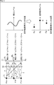
一般的な撮像装置の構成として、例えば、図1の右下部で示されるように、ピンホールカメラが挙げられる。
ピンホールカメラからなる撮像装置は、遮光膜12に対して穴部として設けられたピンホール21と固体撮像素子11から構成される。ピンホールからなる撮像装置の場合、図1の右下部で示されるように、被写体面上のそれぞれ異なる光源から発せられる光線L1乃至L3が、それぞれピンホール21を透過して固体撮像素子11上の画素I1乃至I3に像として撮像される。
ピンホールカメラからなる撮像装置の場合、固体撮像素子11においては、光源のそれぞれから発せられた光線L1乃至L3のうちの1画素分の光線のみにより、像が結像されて固体撮像素子11上の各画素に入射されることになるので暗い画像として撮像される。
そこで、図1の右上部で示されるように、遮光膜31の中央に撮像レンズ32を設けるようにして、撮像レンズ32が、光線L1乃至L3を、光線I11乃至I13で示されるように集光し、固体撮像素子11上にそれぞれの像を結像し、これが固体撮像素子11により撮像されるようにすることを考える。
図1の右上部の場合、固体撮像素子11においては、光線L1乃至L3の全ての光強度の合計である光強度の光からなる像が結像されて固体撮像素子11に入射されることで、固体撮像素子11の各画素において十分な光量の画像として撮像される。
図1の右上部で示されるように、撮像レンズ32を用いることにより、点光源のそれぞれの集合が被写体を構成することになる。したがって、被写体の撮像は、被写体面上の複数の点光源から発せられる光線が集光されて結像される被写体を撮像することになる。
図1の右上部を参照して説明したように、撮像レンズ32の役割は点光源のそれぞれから出射される各光線、即ち拡散光を、固体撮像素子11上に導くことにある。そのため、固体撮像素子11上には最終画像相当の像が結像されることとなり、固体撮像素子11上の各画素において検出される検出信号からなる画像が、像が結像された撮像画像となる。
しかしながら、撮像レンズと撮像レンズの焦点距離によって撮像装置(撮像素子)のサイズが決定されるため、小型化には限界があった。
そこで、図1の左上部で示されるように、撮像レンズやピンホールを設けることなく、固体撮像素子11とマスク51を用いて、被写体面上の被写体を撮像することを考える。
図1の左上部においては、固体撮像素子11の前段に複数のサイズの開口部51aを備えたマスク51が設けられており、光源のそれぞれからの光線L1乃至L3が変調されて固体撮像素子11の撮像面に入射し、固体撮像素子11上の各画素により受光される。
ここで、マスク51においては、開口部51aと遮光部51bとが、図1の左下部で示されるように、単位サイズΔの単位で水平方向および垂直方向について、大きさがランダムに設定されることにより、マスク51上にマスクパターンが形成される。単位サイズΔは、少なくとも画素サイズよりも大きいサイズである。また、固体撮像素子11とマスク51との間には、微小な距離dの隙間が設けられている。また、図1の左下部においては、固体撮像素子11上の画素間のピッチがwとされている。このような構成により、単位サイズΔと距離dとのサイズにより光線L1乃至L3は、固体撮像素子11上に変調されて入射する。
より詳細には、図1の左上部における光線L1乃至L3の光源を、例えば、図2の左上部で示されるように、点光源PA,PB,PCとし、マスク51を透過して入射する固体撮像素子11上の位置Pa,Pb,Pcのそれぞれに光強度a,b,cの光線が入射するものとする。
レンズレス撮像装置の場合、図2の左上部で示されるように、各画素の検出感度は、マスク51に、ランダムに設定される開口部51aより入射光が変調されることにより、入射角に応じた指向性を持つことになる。ここでいう各画素の検出感度に入射角指向性を持たせるとは、固体撮像素子11上の領域に応じて入射光の入射角度に応じた受光感度特性を異なるものとなるように持たせることである。
すなわち、被写体面71を構成する光源が点光源であることを前提とした場合、固体撮像素子11においては、同一の点光源より発せられた同一の光強度の光線が、入射されることになるが、マスク51により変調されることにより、固体撮像素子11の撮像面上の領域毎に入射角度が変化する。そして、マスク51により固体撮像素子11上の領域に応じて入射光の入射角度が変化することにより受光感度特性、すなわち、入射角指向性を有しているので、同一の光強度の光線であっても、固体撮像素子11の撮像面の前段に設けられたマスク51により固体撮像素子11上の領域毎に異なる感度で検出されることになり、領域毎に異なる検出信号レベルの検出信号が検出される。
より具体的には、図2の右上部で示されるように、固体撮像素子11上の位置Pa,Pb,Pcにおける画素の検出信号レベルDA,DB,DCは、それぞれ以下の式(1)乃至式(3)で表される。
DA=α1×a+β1×b+γ1×c
・・・(1)
DB=α2×a+β2×b+γ2×c
・・・(2)
DC=α3×a+β3×b+γ3×c
・・・(3)
・・・(1)
DB=α2×a+β2×b+γ2×c
・・・(2)
DC=α3×a+β3×b+γ3×c
・・・(3)
ここで、α1は、固体撮像素子11上の位置Paにおける復元する被写体面71上の点光源PAからの光線の入射角度に応じて設定される検出信号レベルaに対する係数である。
また、β1は、固体撮像素子11上の位置Paにおける復元する被写体面71上の点光源PBからの光線の入射角度に応じて設定される検出信号レベルbに対する係数である。
さらに、γ1は、固体撮像素子11上の位置Paにおける復元する被写体面71上の点光源PCからの光線の入射角度に応じて設定される検出信号レベルcに対する係数である。
従って、検出信号レベルDAのうちの(α1×a)は、位置Pcにおける点光源PAからの光線による検出信号レベルを示したものである。
また、検出信号レベルDAのうちの(β1×b)は、位置Pcにおける点光源PBからの光線による検出信号レベルを示したものである。
さらに、検出信号レベルDAのうちの(γ1×c)は、位置Pcにおける点光源PCからの光線による検出信号レベルを示したものである。
従って、検出信号レベルDAは、位置Paにおける点光源PA,PB,PCの各成分に、それぞれの係数α1,β1,γ1を掛けたものの合成値として表現される。以降、係数α1、β1、γ1を合わせて係数セットと呼ぶこととする。
同様に、点光源PBにおける検出信号レベルDBについて、係数セットα2,β2,γ2は、それぞれ点光源PAにおける検出信号レベルDAについての、係数セットα1,β1,γ1に対応するものである。また、点光源PCにおける検出信号レベルDCについて、係数セットα3,β3,γ3は、それぞれ点光源PAにおける検出信号レベルDAについての、係数セットα1,β1,γ1に対応するものである。
ただし、位置Pa,Pb,Pcの画素の検出信号レベルについては、点光源PA,PB,PCのそれぞれより発せられた光線の光強度a,b,cと係数との積和により表現される値である。このため、これらの検出信号レベルは、点光源PA,PB,PCのそれぞれより発せられた光線の光強度a,b,cが入り交じったものとなるので、被写体の像が結像されたものとは異なるものである。
すなわち、この係数セットα1,β1,γ1,係数セットα2,β2,γ2,係数セットα3,β3,γ3と、検出信号レベルDA,DB,DCを用いた連立方程式を構成し、光強度a,b,cを解くことで、図2の右下部で示されるように各位置Pa,Pb,Pcの画素値を求める。これにより画素値の集合である復元画像(最終画像)が再構成されて復元される。
また、図2の左上部で示される固体撮像素子11と被写体面71との距離が変化する場合、係数セットα1,β1,γ1,係数セットα2,β2,γ2,係数セットα3,β3,γ3は、それぞれ変化することになるが、この係数セットを変化させることで、様々な距離の被写体面の復元画像(最終画像)を再構成させることができる。
このため、1回の撮像により、係数セットを様々な距離に対応するものに変化させることで、撮像位置から様々な距離の被写体面の画像を再構成することができる。
結果として、レンズレス撮像装置を用いた撮像においては、レンズを用いた撮像装置での撮像において合焦点がずれた状態で撮像される、いわゆる、ピンぼけといった現象を意識する必要がなく、画角内に撮像したい被写体が含まれるように撮像されていれば、距離に応じた係数セットを変化させることで様々な距離の被写体面の画像を、撮像後に再構成することができる。
尚、図1の右上部で示される検出信号レベルは、被写体の像が結像された画像に対応する検出信号レベルではないので、画素値ではない。また、図1の右下部で示される検出信号レベルは、被写体の像が結像された画像に対応する画素毎の信号値、すなわち、復元画像(最終画像)の各画素の値なので、画素値となる。
このような構成により、撮像レンズや、ピンホールを必要としない、いわゆるレンズレス撮像装置を実現することが可能となる。結果として、撮像レンズや、ピンホール等が必須構成とならないので、撮像装置の低背化、すなわち、撮像機能を実現する構成における光の入射方向に対する厚さを薄くすることが可能になる。また、係数セットを様々に変化させることにより、様々な距離の被写体面における最終画像(復元画像)を再構成して復元することが可能となる。
尚、以降においては、固体撮像素子により撮像された、再構成される前の画像を単に撮像画像と称し、撮像画像が信号処理されることにより再構成されて復元される画像を最終画像(復元画像)と称する。従って、1枚の撮像画像からは、上述した係数セットを様々に変化させることにより、様々な距離の被写体面71上の画像を最終画像として再構成させることができる。
しかしながら、レンズレス撮像装置においては、マスク51に設けられた開口部51aにおいては、光線L1乃至L3が入射すると、出射する際に回折が発生することにより、入射光が拡散し、固体撮像素子11上において撮像される画像上においてボケとして現れる。この結果、そのまま再構成して最終画像を求めると、ボケによる影響により、空間解像度の低い画像が最終画像となってしまう。
ところが、回折の影響の大きさは、入射光の波長と開口部51aの大きさを調整する最小単位である単位サイズにより変化させることができる。
そこで、本開示のレンズレス撮像装置においては、マスク51および固体撮像素子11を複数の領域に分割して、マスク51前段に分割領域毎に入射光の波長帯域を変化させるバンドパスフィルタを設けるようにする。そして、回折により生じる入射光の拡散による影響を小さくするように、各領域のバンドパスフィルタにより透過する光の波長帯に応じた単位サイズで、マスク51上に開口部51aのサイズが設けられるようにする。
このような構成により、領域毎に設定される入射光の波長帯に応じて適切に回折の影響を低減させて、領域毎に撮像画像を撮像し、信号処理により各領域の最終画像を再構成して、統合する。結果として、レンズレス撮像装置において、広い入射光の波長帯の入射光による撮像において、回折によるボケの影響を低減し、空間解像度の高い最終画像を再構成することが可能となる。
<<2.本開示の概要>>
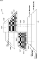
次に、図3を参照して、本開示のレンズレス撮像装置の撮像素子の概要について説明する。尚、図3の左部は、一般的なレンズレス撮像装置における撮像素子の構成例を示しており、左上部がマスク51の上面図であり、左下部がマスク51と固体撮像素子11とを側面上方からみた斜視図である。また、図3の右部は、本開示のレンズレス撮像装置における撮像素子の構成例を示しており、右上部がマスク102の上面図であり、右下部がマスク102の前段にバンドパスフィルタ103が設けられた状態のマスク102と固体撮像素子101とを側面上方からみた斜視図である。
次に、図3を参照して、本開示のレンズレス撮像装置の撮像素子の概要について説明する。尚、図3の左部は、一般的なレンズレス撮像装置における撮像素子の構成例を示しており、左上部がマスク51の上面図であり、左下部がマスク51と固体撮像素子11とを側面上方からみた斜視図である。また、図3の右部は、本開示のレンズレス撮像装置における撮像素子の構成例を示しており、右上部がマスク102の上面図であり、右下部がマスク102の前段にバンドパスフィルタ103が設けられた状態のマスク102と固体撮像素子101とを側面上方からみた斜視図である。
一般的なレンズレス撮像装置の撮像素子は、例えば、図3の左部で示されるように、マスク51における開口部51aの単位サイズが、全領域に対して一様に設定されて、固体撮像素子11においては、マスク51を透過した光より全体として1枚の画像が撮像される。
これに対して、本開示のレンズレス撮像装置の撮像素子は、固体撮像素子101、マスク102、およびバンドパスフィルタ103のそれぞれが、水平方向および垂直方向についてそれぞれ2領域ずつ合計4領域に分割されており、それぞれの領域に入射する入射光の波長帯がそれぞれ異なる、同一の被写体についての4枚の撮像画像が撮像される。
より詳細には、マスク102は、領域102A乃至102Dからなる合計4領域に分割されており、領域102A乃至102Dのそれぞれにおいては、単位サイズが異なる開口部102a乃至102dが設けられている。
また、開口部102a乃至102dのそれぞれの単位サイズは、マスク102の前段に設けられているバンドパスフィルタ103における各領域103A乃至103Dのそれぞれにおいて透過させる光の波長帯に応じてランダムに設定される。
すなわち、領域102Aの開口部102aの単位サイズは、バンドパスフィルタ103の領域103Aが透過させる波長帯の光が透過するとき、回折の影響が最も小さくなる単位サイズに設定される。
また、領域102Bの開口部102bの単位サイズは、バンドパスフィルタ103の領域103Bが透過させる波長帯の光が透過するとき、回折の影響が最も小さくなる単位サイズに設定される。
さらに、領域102Cの開口部102cの単位サイズは、バンドパスフィルタ103の領域103Cが透過させる波長帯の光が透過するとき、回折の影響が最も小さくなる単位サイズに設定される。
また、領域102Dの開口部102dの単位サイズは、バンドパスフィルタ103の領域103Dが透過させる波長帯の光が透過するとき、回折の影響が最も小さくなる単位サイズに設定される。
固体撮像素子101も、領域102A乃至102Dに対応するように、領域101A乃至101Dの4領域に分割されており、固体撮像素子101の領域101Aが、バンドパスフィルタ103の領域103Aが透過させる波長帯の光からなる撮像画像Aを撮像する。
また、固体撮像素子101の領域101Bが、バンドパスフィルタ103の領域103Bが透過させる波長帯の光からなる撮像画像Bを撮像する。
さらに、固体撮像素子101の領域101Cが、バンドパスフィルタ103の領域103Cが透過させる波長帯の光からなる撮像画像Cを撮像する。
また、固体撮像素子101の領域101Dが、バンドパスフィルタ103の領域103Dが透過させる波長の光からなる撮像画像Dを撮像する。
そして、各波長帯における回折によるボケの影響が低減された撮像画像A乃至Dを撮像することが可能となる。また、撮像画像A乃至Dに基づいて、上述したレンズレスの撮像装置における信号処理が施されることにより、最終画像A乃至Dが生成され、最終画像A乃至Dが加算されて、1枚の最終画像に統合されることで、空間解像度の高い1枚の最終画像を復元することが可能となる。
<<3.第1の実施の形態>>
次に、図4を参照して、本開示のレンズレスの撮像装置(レンズレス撮像装置)の構成例について説明する。
次に、図4を参照して、本開示のレンズレスの撮像装置(レンズレス撮像装置)の構成例について説明する。
図4は、本開示のレンズレスの撮像装置111の側面断面の構成例を示している。より詳細には、図4のレンズレスの撮像装置111は、制御部121、撮像素子122、信号処理部123、表示部124、および記憶部125より構成されている。
制御部121は、プロセッサなどより構成されており、レンズレスの撮像装置111の全体の動作を制御している。
撮像素子122は、図3の右部を参照して説明した構成とされており、図4の右向きの矢印で示される被写体からの入射光の光量に応じた画素信号からなる画像を撮像画像として撮像して信号処理部123に出力する。
より詳細には、撮像素子122は、図3の右部に対応しており、図中左からバンドパスフィルタ103、マスク102、および固体撮像素子101より構成される。
バンドパスフィルタ103は、図3を参照して説明したように水平方向および垂直方向にそれぞれ2分割され、すなわち、領域103A乃至103Dの合計4分割にされており、それぞれの領域ごとに入射光のうち異なる波長帯の光を透過させる。
例えば、図5で示されるように、バンドパスフィルタ103の領域103Aは、入射光のうち所定の波長λ1乃至λ1+α付近の波長帯ZAの入射光を透過させ、領域103Bは、入射光のうち所定の波長λ1+α乃至λ1+2α付近の波長帯ZBの入射光を透過させ、領域103Cは、入射光のうち所定の波長λ1+2α乃至λ1+3α付近の波長帯ZCの入射光を透過させ、領域103Dは、入射光のうち所定の波長λ1+3α乃至λ1+4α付近の波長帯ZDの入射光を透過させる。
ここで、λ1は、入射光のうちの所定の波長であり、αは所定の定数である。
したがって、バンドパスフィルタ103の領域103A乃至103Dは、入射光のうち、それぞれ異なる波長帯ZA乃至ZDの入射光を透過させる。尚、波長帯ZA乃至ZDについては、図5において、波長帯の幅がほぼ同一とされているが、同一の幅である必要は無く、異なる幅であってもよい。
マスク102は、図3の右部で示されるように、バンドパスフィルタ103の領域103A乃至103Dに対応するように、領域102A乃至102Dに分割されており、それぞれのマスクにおける遮光部と開口部との間隔を調整する単位サイズΔ(図1の左下部参照)が、透過する光の波長に対応して回折による影響を最小にするように調整される。
例えば、マスク102と固体撮像素子101との間隔が所定の距離dである場合、マスク102を入射光が透過する場合に発生する回折の大きさは、透過する光の波長と開口部のサイズを調整する単位サイズΔにより変化する。
例えば、図6の最上段で示されるように、入射光の波長が波長λ1であるとき、1個の開口部の大きさを、単位サイズΔで、図中の左からΔ1乃至Δ1+7βまで所定の幅β単位で変化させるとき、固体撮像素子101により撮像される、1個の開口部を通過する入射光の撮像画像は、撮像画像F1乃至F8のように変化する。
開口部により回折が発生すると、固体撮像素子101の撮像面においては、入射光に対する入射光の画像が、スポット状の画像にならず、光が散乱されて拡がっているような画像となり、さらに、回折の影響の程度により拡がりの大きさが変化する。
すなわち、図6の最上段における、入射光の波長が波長λ1である場合、撮像画像F4(単位サイズΔ=Δ1+3β)において、スポット径が最も明るく、かつ、最小となり、回折の影響が最小になっているとみなすことができる。また、このとき、撮像画像F3,F2,F1で示されるように、単位サイズΔが小さくなるにしたがって、または、撮像画像F5乃至F8で示されるように単位サイズΔが大きくなるにしたがって、中心付近のスポットが拡がり、回折による影響が徐々に大きくなっていることが示されている。
また、図6の上から2段目で示されるように、入射光の波長が波長λ1+αであるとき、単位サイズΔをΔ1乃至Δ1+7βまで所定の幅β単位で変化させるとき、固体撮像素子101により撮像される、1個の開口部を通過する入射光の撮像画像は、撮像画像F11乃至F18のように変化する。
すなわち、図6の2段目における、入射光の波長が波長λ1+αである場合、撮像画像F15(単位サイズΔ=Δ1+4β)において、スポット径が最も明るく、かつ、最小となり、回折の影響が最小になっているとみなすことができる。また、撮像画像F14,F13,F12,F11で示されるように、単位サイズΔが小さくなるにしたがって、または、撮像画像F16乃至F18で示されるように単位サイズΔが大きくなるにしたがって、中心付近のスポットが拡がり、回折による影響が徐々に大きくなっていることが示されている。
さらに、図6の上から3段目で示されるように、入射光の波長が波長λ1+2αであるとき、単位サイズΔをΔ1乃至Δ1+7βまで所定の幅β単位で変化させるとき、固体撮像素子101により撮像される、1個の開口部を通過する入射光の撮像画像は、撮像画像F21乃至F28のように変化する。
すなわち、図6の3段目における、入射光の波長が波長λ1+2αである場合、撮像画像F25(単位サイズΔ=Δ1+4β)において、スポット径が最も明るく、かつ、最小となり、回折の影響が最小になっているとみなすことができる。また、撮像画像F24,F23,F22,F21で示されるように、単位サイズΔが小さくなるにしたがって、または、撮像画像F26乃至F28で示されるように単位サイズΔが大きくなるにしたがって、中心付近のスポットが拡がり、回折による影響が徐々に大きくなっていることが示されている。
また、図6の上から4段目で示されるように、入射光の波長が波長λ1+3αであるとき、単位サイズΔをΔ1乃至Δ1+7βまで所定の幅β単位で変化させるとき、固体撮像素子101により撮像される、1個の開口部を通過する入射光の撮像画像は、撮像画像F31乃至F38のように変化する。
すなわち、図6の4段目における、入射光の波長が波長λ1+3αである場合、撮像画像F36(単位サイズΔ=Δ1+5β)において、スポット径が最も明るく、かつ、最小となり、回折の影響が最小になっているとみなすことができる。また、撮像画像F35,F34,F33,F32,F31で示されるように、単位サイズΔが小さくなるにしたがって、または、撮像画像F26乃至F28で示されるように単位サイズΔが大きくなるにしたがって、中心付近のスポットが拡がり、回折による影響が徐々に大きくなっていることが示されている。
そこで、バンドパスフィルタ103の領域103A乃至103Dのそれぞれが、図5で示される波長帯ZA乃至ZDのそれぞれの波長帯の光を透過させる場合、対応するマスク102の領域102A乃至102Dの開口部102a乃至102dの単位サイズΔは、それぞれΔ1+3β、Δ1+4β、Δ1+4β、およびΔ1+5βに設定することにより、それぞれの波長帯の光による回折の影響を最小にした状態で入射光を変調させて、固体撮像素子101に入射させることができる。
結果として、固体撮像素子101の領域101A乃至101Dは、それぞれ回折によるボケの影響が最小となる各波長帯の4枚の撮像画像を撮像することが可能となる。
固体撮像素子101は、CMOSイメージセンサなどから構成されており、各画素単位で入射光の光量に応じた画素信号からなる撮像画像を撮像して信号処理部123に出力する。また、固体撮像素子101は、バンドパスフィルタ103およびマスク102のそれぞれの領域103A乃至103Dおよび領域102A乃至102Dに対応するように領域101A乃至101Dに分割されており、それぞれの領域毎に異なる波長帯の入射光からなる同一の範囲の、合計4枚の撮像画像A乃至Dを撮像して信号処理部123に出力する。尚、固体撮像素子101においては、領域101A乃至101Dの範囲において、視差が生じる4枚の同一の撮像画像A乃至Dからなる1枚の撮像画像が撮像されることになるが、ここでは、撮像画像A乃至Dの視差による影響は無視して説明を進めるものとする。
信号処理部123は、撮像素子122より供給される撮像画像A乃至Dの画像信号に対して、例えば、図2および式(1)乃至式(3)を用いて説明したように、連立方程式を解くことにより、領域101A乃至101Dのそれぞれについて最終画像A乃至Dを再構成して統合し、1枚の最終画像として表示部124に出力して表示させる、または、記憶部125に記憶させる。
尚、信号処理部123の詳細な構成については、図7を参照して、詳細を後述する。
<信号処理部の構成例>
次に、図7を参照して、信号処理部123の詳細な構成例について説明する。
次に、図7を参照して、信号処理部123の詳細な構成例について説明する。
信号処理部123は、信号領域分割部131、画像再構成部132、および画像統合部133を備えている。
信号領域分割部131は、撮像素子122より供給されてくる画像を領域101A乃至101Dのそれぞれの領域の画素信号からなる撮像画像A乃至Dに分割して、それぞれ画像再構成部132の画像再構成処理部151A乃至151Dに出力する。
画像再構成部132は、信号領域分割部131により領域101A乃至101Dのそれぞれに分割された4枚の撮像画像A乃至Dのそれぞれを、図2および式(1)乃至式(3)を参照して説明したように、連立方程式を解くことにより最終画像A乃至Dとして再構成し、再構成した最終画像A乃至Dを画像統合部133に出力する。
より詳細には、画像再構成部132は、信号領域分割部131により分割された領域101A乃至101Dのそれぞれの撮像画像A乃至Dより最終画像A乃至Dを再構成する画像再構成処理部151A乃至151Dを備えている。画像再構成処理部151A乃至151Dは、それぞれ信号領域分割部131により分割された領域101A乃至101Dのそれぞれの撮像画像A乃至Dより最終画像A乃至Dを再構成し、画像統合部133に出力する。
画像統合部133は、画像再構成部132の画像再構成処理部151A乃至151Dより供給される固体撮像素子101における領域101A乃至101Dの撮像画像A乃至Dより再構成された最終画像A乃至Dを重ね合わせるように統合して1枚の画像にして表示部124に出力して表示させる、および記憶部125に出力して記憶させる。
<撮像処理>
次に、図8のフローチャートを参照して、図1のレンズレスの撮像装置111による撮像処理について説明する。
次に、図8のフローチャートを参照して、図1のレンズレスの撮像装置111による撮像処理について説明する。
ステップS11において、バンドパスフィルタ103における各領域103A乃至103Dのそれぞれが、入射光のうち、図2を参照して説明した、それぞれの波長帯ZA乃至ZDの光を透過させる。
ステップS12において、マスク102における、各領域102A乃至102Dのそれぞれが、単位サイズΔに応じた開口部102a乃至102dにより、入射光を変調して固体撮像素子101の撮像面に入射させる。
ステップS13において、固体撮像素子101における、領域101A乃至101Dのそれぞれが、マスク102の領域102A乃至102Dを透過することにより変調された光からなる撮像画像A乃至Dを撮像して1枚の撮像画像として信号処理部123に出力する。
ステップS14において、信号処理部123の信号領域分割部131は、撮像素子122の固体撮像素子101より供給されてくる撮像画像を、領域101A乃至101Dのそれぞれに対応する領域の撮像画像A乃至Dに分割し、それぞれを画像再構成部132の画像再構成処理部151A乃至151Dに出力する。
ステップS15において、画像再構成処理部151A乃至151Dは、それぞれ固体撮像素子101における領域101A乃至101Dにより撮像された撮像画像A乃至Dを、図2および式(1)乃至式(3)を参照して説明した処理により再構成し、最終画像A乃至Dを生成して画像統合部133に出力する。
ステップS16において、画像統合部133は、領域101A乃至101Dにより撮像された4枚の撮像画像A乃至Dのそれぞれより求められた最終画像A乃至Dを重ね合わせるようにして統合し、1枚の最終画像として出力する。
以上の処理により、入射光の波長帯に応じたマスク102の各領域102A乃至102Dの単位サイズΔに応じたサイズの開口部と遮光部とにより光が変調されることにより、回折による影響が最小となった状態で、それぞれの波長帯の撮像画像A乃至Dを撮像することが可能となり、撮像された撮像画像A乃至Dより最終画像A乃至Dを再構成することが可能となる。結果として、再構成される最終画像A乃至Dにおいても、回折によるボケの影響を低減させることが可能となり、空間解像度の高い最終画像を生成することが可能となる。
特に、長波長帯の光による回折の影響は大きいため、長波長帯の光における回折の影響によるボケの発生を効果的に抑制することが可能となる。
例えば、温度情報を撮像可能なことで知られている遠赤外線の画像センシング(サーモグラフィセンシング)においては、広範囲の長波長帯の積分された光のピーク波長によって対象の温度が決定される。より具体的には、センシングされる波長帯の範囲は、一般に8μm乃至14μm周辺とされている。この場合、センシング対象の最短波長から、最長波長までの波長差は約2倍となる。
また、可視光と近赤外光を同時に撮像するような撮像系も近年多くのものが存在するが、この場合にも、最短波長となる450nmをピークに持つ青色と、最長波長となる800nmをピークに持つ近赤外光との波長差は、約2倍となる。
このように、広範囲の波長帯の光を積分して露光する場合、広範囲の波長帯の全域に対して、回折によるボケの影響を低減するための最適化を図るのは困難となる。例えば、短波長側の点広がりを小さくするような変調を設計する場合、長波長側の点広がりは大きくなり画像の空間解像度は低下する。その逆の場合も同様であり、高い空間解像度の画像復元は難しくなる。
そこで、例えば、温度情報を撮像可能な画像センシングをする場合、上述した図5の波長λ1を8μmとし、αを1.5μmとして、波長帯ZA乃至ZDを、8μm乃至9.5μm、9.5μm乃至11μm、11μm乃至12.5μm、12.5μm乃至14μmの近傍付近となるように設定することで、近赤外光から遠赤外光の範囲を適切な波長帯として設定することができる。また、それぞれの波長帯において回折の影響が小さくなるようにマスク102の領域102A乃至102Dのそれぞれの単位サイズΔを設定することで、回折によるボケの影響を低減させた温度情報の撮像を実現することが可能となる。
また、上述した波長帯ZA乃至ZDは、これ以外の波長帯に設定されるものであってもよく、例えば、RGB(赤、緑、青の可視光)およびIR(赤外光)となるように設定するようにしてもよい。
さらに、以上においては、バンドパスフィルタ103、マスク102、および固体撮像素子101のそれぞれを、波長帯に応じて、4つの領域に分割して、それぞれの領域において撮像画像A乃至Dを撮像し、撮像画像A乃至Dを用いた信号処理により、最終画像A乃至Dを再構成して、1枚の最終画像に統合する例について説明してきた。しかしながら、分割領域は、4つ以外の数であってもよく、解像度の大きな低下を招かない程度であれば、さらに多くの数に分割するようにしてもよい。また、最終的に統合するため、各領域のサイズは、略同一であることが望ましいが、厳密に同一でなくてもよく、最終画像において必要な範囲を全ての撮像画像が含んでいればよい。
さらに、画像統合部133は、複数の画像を統合する際、1枚の固体撮像素子101における複数の領域で撮像される画像の位置に応じた視差補正を行った後に、統合するようにしてもよい。これにより、より空間解像度を向上させることが可能となる。
また、以上においては、画像統合部133が、複数の再構成された最終画像を重ねるようにして1枚の画像に統合する例について説明してきたが、複数の最終画像を用いて1枚の画像を最終的に生成することができれば統合しているものとみなしてよい。
したがって、画像統合部133は、例えば、複数の最終画像のうち、いずれか1枚の最終画像を選択することで、複数の最終画像を統合してもよい。ここで選択される1枚の最終画像は、例えば、回折の影響が最も小さな画像であってもよい。
また、画像統合部133は、例えば、複数の最終画像のうち、いずれか複数の最終画像を選択し、選択した最終画像を重ね合わせるようにすることで、複数の最終画像を統合してもよい。ここで選択されるいずれか複数の最終画像は、例えば、回折の影響が比較的小さな複数の最終画像であってもよい。
<<4.第2の実施の形態>>
以上においては、バンドパスフィルタ103、マスク102、および固体撮像素子101のそれぞれを対応する複数の領域に分割し、分割された領域毎にバンドパスフィルタ103により透過させる入射光の波長帯を設定し、領域毎の波長帯に応じた単位サイズにより構成される開口部からなるマスク102により入射光を変調させることで、回折による影響を低減した状態で領域毎に撮像画像を撮像し、領域毎に撮像した撮像画像から最終画像を再構成して、各領域の最終画像を統合することで、回折によるボケの影響を低減させることで、空間解像度の高い1枚の最終画像を撮像する例について説明してきた。
以上においては、バンドパスフィルタ103、マスク102、および固体撮像素子101のそれぞれを対応する複数の領域に分割し、分割された領域毎にバンドパスフィルタ103により透過させる入射光の波長帯を設定し、領域毎の波長帯に応じた単位サイズにより構成される開口部からなるマスク102により入射光を変調させることで、回折による影響を低減した状態で領域毎に撮像画像を撮像し、領域毎に撮像した撮像画像から最終画像を再構成して、各領域の最終画像を統合することで、回折によるボケの影響を低減させることで、空間解像度の高い1枚の最終画像を撮像する例について説明してきた。
しかしながら、回折の影響の程度は、入射光の波長帯に応じて、マスク102と固体撮像素子101との距離により調整することもできる。そこで、マスク102の開口部を同一の単位サイズΔで全領域において形成し、入射光の波長帯に応じた領域毎に、マスク102と固体撮像素子101との距離を変えて回折による影響を低減するようにしてもよい。
図9は、マスク102に形成される開口部を全領域において、同一の単位サイズΔで形成し、入射光の波長帯に応じた領域毎に、マスク102と固体撮像素子101との距離を変えて回折による影響を低減するレンズレスの撮像装置111の撮像素子122の構成例を示している。
尚、図9において、図3と同一の機能を備えた構成については、同一の符号を付しており、その説明は適宜省略する。すなわち、図9においては、図3と異なる点は、マスク102の領域102A乃至領域102Dおよびバンドパスフィルタ103の領域103A乃至103Dに代えて、領域102A’乃至102D’、および領域103A’乃至103D’が設定されている点である。また、図9においては、領域102A’,102B’には、マスクパターンの記載が省略されているが、説明の便宜上省略されているのみであり、現実には、領域102A’乃至102D’には、同一の単位サイズのマスクパターンが設けられている。
図9においては、固体撮像素子101の各領域101A乃至101Dと、それぞれのマスク102における領域102A’乃至102D’との距離が領域毎に異なる。
すなわち、図9においては、固体撮像素子101の領域101Aとマスク102の領域102A’との距離は、距離GapAであり、固体撮像素子101の領域101Bとマスク102の領域102B’との距離は、距離GapBであり、固体撮像素子101の領域101Cとマスク102の領域102C’との距離は、距離GapCであり、固体撮像素子101の領域101Dとマスク102の領域102D’との距離は、距離GapDであり、GapA乃至GapDは、それぞれ異なる距離とされている。
これは、回折の影響の程度が、入射光の波長帯に応じて、マスク102と固体撮像素子101との距離により調整することができるためである。
例えば、マスク102の開口部を調整する単位サイズΔが、全領域について所定の同一値とした場合、図10の最上段で示されるように、入射光の波長が波長λ1である場合、マスク102と固体撮像素子101との距離をG1乃至G1+11γまで変化させるとき、固体撮像素子101により撮像される、1個の開口部を通過する入射光の撮像画像は、撮像画像F101乃至F108のように変化する。
開口部により回折が発生すると、固体撮像素子101の撮像面においては、入射光に対する入射光の画像が、スポット状の画像にならず、光が散乱されて拡がっているような画像となり、さらに、回折の影響の程度により拡がりの大きさが変化する。
すなわち、図10の最上段における、入射光の波長が波長λ1である場合、画像F106(マスク102と固体撮像素子101との距離=G1+9γ)において、スポット径が最も明るく、かつ、最小となり、回折の影響が最小になっているとみなすことができる。また、このとき、画像F105乃至F101で示されるように、マスク102と固体撮像素子101との距離が小さくなるにしたがって、または、画像F107で示されるように、マスク102と固体撮像素子101との距離が大きくなるにしたがって、中心付近のスポットが拡がり、回折による影響が徐々に大きくなっていることが示されている。
また、図10の2段目で示されるように、入射光の波長が波長λ1+αである場合、マスク102と固体撮像素子101との距離をG1乃至G1+11γまで変化させるとき、固体撮像素子101により撮像される、1個の開口部を通過する入射光の撮像画像は、撮像画像F111乃至F118のように変化する。
すなわち、図10の2段目における、入射光の波長が波長λ1+αである場合、撮像画像F115(マスク102と固体撮像素子101との距離=G1+7γ)において、スポット径が最も明るく、かつ、最小となり、回折の影響が最小になっているとみなすことができる。また、このとき、撮像画像F114乃至F111で示されるように、マスク102と固体撮像素子101との距離が小さくなるにしたがって、または、撮像画像F116,F117で示されるように、マスク102と固体撮像素子101との距離が大きくなるにしたがって、中心付近のスポットが拡がり、回折による影響が徐々に大きくなっていることが示されている。
さらに、図10の3段目で示されるように、入射光の波長が波長λ1+2αである場合、マスク102と固体撮像素子101との距離をG1乃至G1+11γまで変化させるとき、固体撮像素子101により撮像される、1個の開口部を通過する入射光の撮像画像は、撮像画像F121乃至F128のように変化する。
すなわち、図10の3段目における、入射光の波長が波長λ1+2αである場合、撮像画像F124(マスク102と固体撮像素子101との距離=G1+5γ)において、スポット径が最も明るく、かつ、最小となり、回折の影響が最小になっているとみなすことができる。また、このとき、撮像画像F123乃至F121で示されるように、マスク102と固体撮像素子101との距離が小さくなるにしたがって、または、撮像画像F125乃至F127で示されるように、マスク102と固体撮像素子101との距離が大きくなるにしたがって、中心付近のスポットが拡がり、回折による影響が徐々に大きくなっていることが示されている。
また、図10の4段目で示されるように、入射光の波長が波長λ1+3αである場合、マスク102と固体撮像素子101との距離をG1乃至G1+11γまで変化させるとき、固体撮像素子101により撮像される、1個の開口部を通過する入射光の撮像画像は、撮像画像F131乃至F138のように変化する。
すなわち、図10の4段目における、入射光の波長が波長λ1+3αである場合、撮像画像F133(マスク102と固体撮像素子101との距離=G1+3γ)において、スポット径が最も明るく、かつ、最小となり、回折の影響が最小になっているとみなすことができる。また、このとき、撮像画像F132,F131で示されるように、マスク102と固体撮像素子101との距離が小さくなるにしたがって、または、撮像画像F134乃至F137で示されるように、マスク102と固体撮像素子101との距離が大きくなるにしたがって、中心付近のスポットが拡がり、回折による影響が徐々に大きくなっていることが示されている。
そこで、図9のバンドパスフィルタ103の領域103A’乃至103D’のそれぞれが、図5で示される波長帯ZA乃至ZDのそれぞれの波長帯の光を透過させる場合、対応するマスク102の領域102A’乃至102D’と固体撮像素子101の領域101A乃至101Dとのそれぞれの距離GapA乃至Dを、G1+9γ、G1+7γ、G1+5γ、およびG1+3γに設定することにより、それぞれの波長帯における光による回折を最小にした状態で入射光を変調させて、固体撮像素子101に入射させることができる。
結果として、固体撮像素子101は、回折によるボケの影響が最小となる各波長帯の4枚の撮像画像を撮像することが可能となる。
尚、図9を参照して説明した構成の撮像素子122を用いたレンズレスの撮像装置111における撮像処理については、図8のフローチャートを参照して説明した処理と同様であるので、その説明は省略するものとする。
また、透過する波長帯に応じて、回折の影響が最小となるようにバンドパスフィルタ103、マスク102、および固体撮像素子101を構成できればよいので、透過する波長帯が同一の領域毎に、マスク102の単位サイズと、マスク102および固体撮像素子101間の距離との両方を調整するようにしてもよい。
<<5.第3の実施の形態>>
以上においては、バンドパスフィルタ103、マスク102、および固体撮像素子101のそれぞれを、バンドパスフィルタ103により透過させる光の波長帯に応じた領域に、分割して、それぞれの領域において、波長帯毎に回折の影響が最小となるようにして、それぞれの領域においてマスク102により変調し、固体撮像素子101により撮像し、撮像した領域毎の撮像画像より、各領域の最終画像を再構成して、1枚の最終画像として統合する例について説明してきた。
以上においては、バンドパスフィルタ103、マスク102、および固体撮像素子101のそれぞれを、バンドパスフィルタ103により透過させる光の波長帯に応じた領域に、分割して、それぞれの領域において、波長帯毎に回折の影響が最小となるようにして、それぞれの領域においてマスク102により変調し、固体撮像素子101により撮像し、撮像した領域毎の撮像画像より、各領域の最終画像を再構成して、1枚の最終画像として統合する例について説明してきた。
しかしながら、各領域の境界付近においては、異なる波長帯の光が混色してしまう恐れがあり、境界付近において適切に回折の影響を低減できない恐れがある。
そこで、分割された領域の境界に遮光壁を設けるようにして、異なる波長帯の光の混色を防止するようにして、各波長帯の領域毎に、適切に回折の影響を低減できるようにしてもよい。
図11は、分割された領域の境界に遮光壁を設けるようにしたレンズレスの撮像装置111の撮像素子122の構成例を示している。尚、図11において、図3と同一の機能を備えた構成については、同一の符号を付しており、その説明は省略する。
すなわち、図11において、図3のレンズレス撮像装置の撮像素子と異なる点は、バンドパスフィルタ103の領域103A乃至130D、マスク102の領域102A乃至102D、および、固体撮像素子101の領域101A乃至101Dのそれぞれの境界に、遮光壁201-1,201-2が設けられている点である。
遮光壁201-1,201-2が、バンドパスフィルタ103の領域103A乃至130D、マスク102の領域102A乃至102D、および、固体撮像素子101の領域101A乃至101Dのそれぞれの境界に設けられることにより、各領域の境界付近における隣接する波長帯の光による混色を防止することが可能となり、各領域において、確実に回折による影響を低減させることが可能となる。
結果として、各領域における波長帯の入射光により回折に起因するボケの影響を低減して撮像画像を撮像することが可能となるので、撮像画像に基づいて再構成される最終画像の空間解像度を高めることが可能となる。
尚、本明細書において、システムとは、複数の構成要素(装置、モジュール(部品)等)の集合を意味し、すべての構成要素が同一筐体中にあるか否かは問わない。したがって、別個の筐体に収納され、ネットワークを介して接続されている複数の装置、及び、1つの筐体の中に複数のモジュールが収納されている1つの装置は、いずれも、システムである。
また、本開示の実施の形態は、上述した実施の形態に限定されるものではなく、本開示の要旨を逸脱しない範囲において種々の変更が可能である。
さらに、上述のフローチャートで説明した各ステップは、1つの装置で実行する他、複数の装置で分担して実行することができる。
また、1つのステップに複数の処理が含まれる場合には、その1つのステップに含まれる複数の処理は、1つの装置で実行する他、複数の装置で分担して実行することができる。
尚、本開示は、以下のような構成も取ることができる。
<1> 複数の領域に分割され、前記領域毎に異なる波長帯の入射光を透過させるバンドパスフィルタと、
前記複数の領域に対応して分割され、前記バンドパスフィルタを透過した、前記領域毎に異なる波長帯の入射光を変調するマスクと、
前記複数の領域に対応して撮像面が分割され、前記領域毎に前記マスクにより変調された入射光を2次元の画素信号として撮像する固体撮像素子と、
前記固体撮像素子により撮像された2次元の画素信号を、信号処理により最終画像として再構成する信号処理部と
を含む撮像装置。
<2> 前記マスクは、前記領域毎に異なる単位サイズのマスクパターンである
<1>に記載の撮像装置。
<3> 前記領域毎の、前記マスクパターンは、前記バンドパスフィルタを透過する入射光の波長帯に基づいた、異なる単位サイズのマスクパターンである
<2>に記載の撮像装置。
<4> 前記領域毎の、前記マスクパターンは、前記バンドパスフィルタを透過する波長帯の入射光が、前記固体撮像素子により撮像されるとき、回折による前記入射光の拡散が略最小となる単位サイズのマスクパターンである
<2>に記載の撮像装置。
<5> 前記マスクから前記固体撮像素子の撮像面までの距離は、前記領域毎に異なる距離である
<1>に記載の撮像装置。
<6> 前記マスクから前記固体撮像素子の撮像面までの距離は、前記領域毎の、前記バンドパスフィルタを透過する入射光の波長帯に基づいた異なる距離である
<5>に記載の撮像装置。
<7> 前記領域毎の、前記マスクから前記固体撮像素子の撮像面までの距離は、前記バンドパスフィルタを透過する波長帯の入射光が、前記固体撮像素子により撮像されるとき、回折による前記入射光の拡散が略最小となる距離である
<6>に記載の撮像装置。
<8> 前記マスクは、全ての前記領域について、同一の単位サイズのマスクパターンである
<5>に記載の撮像装置。
<9> 前記バンドパスフィルタ、前記マスク、および前記固体撮像素子における、前記複数の領域における境界において、隣接する領域からの入射光を遮光する遮光壁をさらに含む
<1>に記載の撮像装置。
<10> 前記信号処理部は、
前記固体撮像素子により撮像された2次元の画素信号を、前記複数の領域に対応付けて分割する分割部と、
分割された前記2次元の画素信号のそれぞれについて、信号処理により最終画像として再構成する複数の画像再構成部と、
前記複数の画像再構成部により再構成された最終画像を統合する統合部とを含む
<1>に記載の撮像装置。
<11> 前記統合部は、前記複数の画像再構成部により再構成された最終画像を重ね合わせることにより統合する
<10>に記載の撮像装置。
<12> 前記統合部は、前記複数の画像再構成部により再構成された最終画像のいずれか1枚を選択することにより統合する
<10>に記載の撮像装置。
<13> 前記統合部は、前記複数の画像再構成部により再構成された最終画像の少なくとも2枚以上を選択し、選択した前記最終画像を重ね合わせるようにして統合する
<10>に記載の撮像装置。
<14> 前記固体撮像素子と、前記マスクとの間には、前記入射光の入射方向に対して微細な隙間がある
<1>に記載の撮像装置。
<15> 前記入射光を前記バンドパスフィルタ、前記マスク、および前記固体撮像素子のいずれに対しても合焦させるレンズを含まない
<1>に記載の撮像装置。
<16> 前記入射光の波長帯は、約8μm乃至約14μmである
<1>に記載の撮像装置。
<17> 複数の領域に分割され、前記領域毎に異なる波長帯の入射光を透過させるバンドパスフィルタと、
前記複数の領域に対応して分割され、前記バンドパスフィルタを透過した、前記領域毎に異なる波長帯の入射光を変調するマスクと、
前記複数の領域に対応して撮像面が分割され、前記領域毎に前記マスクにより変調された入射光を2次元の画素信号として撮像する固体撮像素子とを含む撮像装置の撮像方法であって、
前記固体撮像素子により撮像された2次元の画素信号を、信号処理により最終画像として再構成する信号処理
を含む撮像方法。
<18> 複数の領域に分割され、前記領域毎に異なる波長帯の入射光を透過させるバンドパスフィルタと、
前記複数の領域に対応して分割され、前記バンドパスフィルタを透過した、前記領域毎に異なる波長帯の入射光を変調するマスクと、
前記複数の領域に対応して撮像面が分割され、前記領域毎に前記マスクにより変調された入射光を2次元の画素信号として撮像する固体撮像素子とを含む
撮像素子。
前記複数の領域に対応して分割され、前記バンドパスフィルタを透過した、前記領域毎に異なる波長帯の入射光を変調するマスクと、
前記複数の領域に対応して撮像面が分割され、前記領域毎に前記マスクにより変調された入射光を2次元の画素信号として撮像する固体撮像素子と、
前記固体撮像素子により撮像された2次元の画素信号を、信号処理により最終画像として再構成する信号処理部と
を含む撮像装置。
<2> 前記マスクは、前記領域毎に異なる単位サイズのマスクパターンである
<1>に記載の撮像装置。
<3> 前記領域毎の、前記マスクパターンは、前記バンドパスフィルタを透過する入射光の波長帯に基づいた、異なる単位サイズのマスクパターンである
<2>に記載の撮像装置。
<4> 前記領域毎の、前記マスクパターンは、前記バンドパスフィルタを透過する波長帯の入射光が、前記固体撮像素子により撮像されるとき、回折による前記入射光の拡散が略最小となる単位サイズのマスクパターンである
<2>に記載の撮像装置。
<5> 前記マスクから前記固体撮像素子の撮像面までの距離は、前記領域毎に異なる距離である
<1>に記載の撮像装置。
<6> 前記マスクから前記固体撮像素子の撮像面までの距離は、前記領域毎の、前記バンドパスフィルタを透過する入射光の波長帯に基づいた異なる距離である
<5>に記載の撮像装置。
<7> 前記領域毎の、前記マスクから前記固体撮像素子の撮像面までの距離は、前記バンドパスフィルタを透過する波長帯の入射光が、前記固体撮像素子により撮像されるとき、回折による前記入射光の拡散が略最小となる距離である
<6>に記載の撮像装置。
<8> 前記マスクは、全ての前記領域について、同一の単位サイズのマスクパターンである
<5>に記載の撮像装置。
<9> 前記バンドパスフィルタ、前記マスク、および前記固体撮像素子における、前記複数の領域における境界において、隣接する領域からの入射光を遮光する遮光壁をさらに含む
<1>に記載の撮像装置。
<10> 前記信号処理部は、
前記固体撮像素子により撮像された2次元の画素信号を、前記複数の領域に対応付けて分割する分割部と、
分割された前記2次元の画素信号のそれぞれについて、信号処理により最終画像として再構成する複数の画像再構成部と、
前記複数の画像再構成部により再構成された最終画像を統合する統合部とを含む
<1>に記載の撮像装置。
<11> 前記統合部は、前記複数の画像再構成部により再構成された最終画像を重ね合わせることにより統合する
<10>に記載の撮像装置。
<12> 前記統合部は、前記複数の画像再構成部により再構成された最終画像のいずれか1枚を選択することにより統合する
<10>に記載の撮像装置。
<13> 前記統合部は、前記複数の画像再構成部により再構成された最終画像の少なくとも2枚以上を選択し、選択した前記最終画像を重ね合わせるようにして統合する
<10>に記載の撮像装置。
<14> 前記固体撮像素子と、前記マスクとの間には、前記入射光の入射方向に対して微細な隙間がある
<1>に記載の撮像装置。
<15> 前記入射光を前記バンドパスフィルタ、前記マスク、および前記固体撮像素子のいずれに対しても合焦させるレンズを含まない
<1>に記載の撮像装置。
<16> 前記入射光の波長帯は、約8μm乃至約14μmである
<1>に記載の撮像装置。
<17> 複数の領域に分割され、前記領域毎に異なる波長帯の入射光を透過させるバンドパスフィルタと、
前記複数の領域に対応して分割され、前記バンドパスフィルタを透過した、前記領域毎に異なる波長帯の入射光を変調するマスクと、
前記複数の領域に対応して撮像面が分割され、前記領域毎に前記マスクにより変調された入射光を2次元の画素信号として撮像する固体撮像素子とを含む撮像装置の撮像方法であって、
前記固体撮像素子により撮像された2次元の画素信号を、信号処理により最終画像として再構成する信号処理
を含む撮像方法。
<18> 複数の領域に分割され、前記領域毎に異なる波長帯の入射光を透過させるバンドパスフィルタと、
前記複数の領域に対応して分割され、前記バンドパスフィルタを透過した、前記領域毎に異なる波長帯の入射光を変調するマスクと、
前記複数の領域に対応して撮像面が分割され、前記領域毎に前記マスクにより変調された入射光を2次元の画素信号として撮像する固体撮像素子とを含む
撮像素子。
101 固体撮像素子, 101A乃至101D,101A’乃至101D’ 領域, 102 マスク, 102A乃至102D,102A’乃至102D’ 領域, 103 バンドパスフィルタ, 103A乃至103D,103A’乃至103D’ 領域, 111 レンズレス撮像装置, 121 制御部, 122 撮像素子, 123 信号処理部, 124 表示部, 125 記憶部, 131 信号領域分割部, 132 画像再構成部, 133 画像統合部, 151A乃至151D 画像再構成処理部
Claims (18)
- 複数の領域に分割され、前記領域毎に異なる波長帯の入射光を透過させるバンドパスフィルタと、
前記複数の領域に対応して分割され、前記バンドパスフィルタを透過した、前記領域毎に異なる波長帯の入射光を変調するマスクと、
前記複数の領域に対応して撮像面が分割され、前記領域毎に前記マスクにより変調された入射光を2次元の画素信号として撮像する固体撮像素子と、
前記固体撮像素子により撮像された2次元の画素信号を、信号処理により最終画像として再構成する信号処理部と
を含む撮像装置。 - 前記マスクは、前記領域毎に異なる単位サイズのマスクパターンである
請求項1に記載の撮像装置。 - 前記領域毎の、前記マスクパターンは、前記バンドパスフィルタを透過する入射光の波長帯に基づいた、異なる単位サイズのマスクパターンである
請求項2に記載の撮像装置。 - 前記領域毎の、前記マスクパターンは、前記バンドパスフィルタを透過する波長帯の入射光が、前記固体撮像素子により撮像されるとき、回折による前記入射光の拡散が略最小となる単位サイズのマスクパターンである
請求項2に記載の撮像装置。 - 前記マスクから前記固体撮像素子の撮像面までの距離は、前記領域毎に異なる距離である
請求項1に記載の撮像装置。 - 前記マスクから前記固体撮像素子の撮像面までの距離は、前記領域毎の、前記バンドパスフィルタを透過する入射光の波長帯に基づいた異なる距離である
請求項5に記載の撮像装置。 - 前記領域毎の、前記マスクから前記固体撮像素子の撮像面までの距離は、前記バンドパスフィルタを透過する波長帯の入射光が、前記固体撮像素子により撮像されるとき、回折による前記入射光の拡散が略最小となる距離である
請求項6に記載の撮像装置。 - 前記マスクは、全ての前記領域について、同一の単位サイズのマスクパターンである
請求項5に記載の撮像装置。 - 前記バンドパスフィルタ、前記マスク、および前記固体撮像素子における、前記複数の領域における境界において、隣接する領域からの入射光を遮光する遮光壁をさらに含む
請求項1に記載の撮像装置。 - 前記信号処理部は、
前記固体撮像素子により撮像された2次元の画素信号を、前記複数の領域に対応付けて分割する分割部と、
分割された前記2次元の画素信号のそれぞれについて、信号処理により最終画像として再構成する複数の画像再構成部と、
前記複数の画像再構成部により再構成された最終画像を統合する統合部とを含む
請求項1に記載の撮像装置。 - 前記統合部は、前記複数の画像再構成部により再構成された最終画像を重ね合わせることにより統合する
請求項10に記載の撮像装置。 - 前記統合部は、前記複数の画像再構成部により再構成された最終画像のいずれか1枚を選択することにより統合する
請求項10に記載の撮像装置。 - 前記統合部は、前記複数の画像再構成部により再構成された最終画像の少なくとも2枚以上を選択し、選択した前記最終画像を重ね合わせるようにして統合する
請求項10に記載の撮像装置。 - 前記固体撮像素子と、前記マスクとの間には、前記入射光の入射方向に対して微細な隙間がある
請求項1に記載の撮像装置。 - 前記入射光を前記バンドパスフィルタ、前記マスク、および前記固体撮像素子のいずれに対しても合焦させるレンズを含まない
請求項1に記載の撮像装置。 - 前記入射光の波長帯は、約8μm乃至約14μmである
請求項1に記載の撮像装置。 - 複数の領域に分割され、前記領域毎に異なる波長帯の入射光を透過させるバンドパスフィルタと、
前記複数の領域に対応して分割され、前記バンドパスフィルタを透過した、前記領域毎に異なる波長帯の入射光を変調するマスクと、
前記複数の領域に対応して撮像面が分割され、前記領域毎に前記マスクにより変調された入射光を2次元の画素信号として撮像する固体撮像素子とを含む撮像装置の撮像方法であって、
前記固体撮像素子により撮像された2次元の画素信号を、信号処理により最終画像として再構成する信号処理
を含む撮像方法。 - 複数の領域に分割され、前記領域毎に異なる波長帯の入射光を透過させるバンドパスフィルタと、
前記複数の領域に対応して分割され、前記バンドパスフィルタを透過した、前記領域毎に異なる波長帯の入射光を変調するマスクと、
前記複数の領域に対応して撮像面が分割され、前記領域毎に前記マスクにより変調された入射光を2次元の画素信号として撮像する固体撮像素子とを含む
撮像素子。
Priority Applications (4)
| Application Number | Priority Date | Filing Date | Title |
|---|---|---|---|
| EP18892750.3A EP3731521B1 (en) | 2017-12-22 | 2018-12-07 | Imaging device, imaging method, and imaging element |
| JP2019560961A JP7283394B2 (ja) | 2017-12-22 | 2018-12-07 | 撮像装置、および撮像方法、並びに撮像素子 |
| US16/954,015 US11283993B2 (en) | 2017-12-22 | 2018-12-07 | Image-capturing apparatus, image-capturing method, and image-capturing device |
| CN201880079342.3A CN111448796B (zh) | 2017-12-22 | 2018-12-07 | 图像拍摄装置、图像拍摄方法、图像拍摄器件和存储介质 |
Applications Claiming Priority (2)
| Application Number | Priority Date | Filing Date | Title |
|---|---|---|---|
| JP2017246393 | 2017-12-22 | ||
| JP2017-246393 | 2017-12-22 |
Publications (1)
| Publication Number | Publication Date |
|---|---|
| WO2019124106A1 true WO2019124106A1 (ja) | 2019-06-27 |
Family
ID=66992576
Family Applications (1)
| Application Number | Title | Priority Date | Filing Date |
|---|---|---|---|
| PCT/JP2018/045019 Ceased WO2019124106A1 (ja) | 2017-12-22 | 2018-12-07 | 撮像装置、および撮像方法、並びに撮像素子 |
Country Status (5)
| Country | Link |
|---|---|
| US (1) | US11283993B2 (ja) |
| EP (1) | EP3731521B1 (ja) |
| JP (1) | JP7283394B2 (ja) |
| CN (1) | CN111448796B (ja) |
| WO (1) | WO2019124106A1 (ja) |
Cited By (6)
| Publication number | Priority date | Publication date | Assignee | Title |
|---|---|---|---|---|
| CN111128046A (zh) * | 2020-01-16 | 2020-05-08 | 浙江大学 | 一种led显示屏幕的无透镜成像装置及方法 |
| WO2022130689A1 (ja) * | 2020-12-18 | 2022-06-23 | 株式会社フジクラ | 光回折素子、光演算システム、及び、光回折素子の製造方法 |
| WO2023145444A1 (ja) * | 2022-01-27 | 2023-08-03 | ソニーグループ株式会社 | 撮像装置、および撮像装置の作動方法 |
| US11994689B2 (en) | 2019-10-18 | 2024-05-28 | Google Llc | Diffractive optical elements for large-field image display |
| WO2025047424A1 (ja) * | 2023-08-30 | 2025-03-06 | ソニーセミコンダクタソリューションズ株式会社 | 撮像装置 |
| US12499553B2 (en) | 2020-12-08 | 2025-12-16 | Sony Group Corporation | Image processing apparatus and image processing method |
Families Citing this family (6)
| Publication number | Priority date | Publication date | Assignee | Title |
|---|---|---|---|---|
| FR3077641B1 (fr) * | 2018-02-07 | 2020-02-21 | TiHive | Systeme d'imagerie terahertz a reflexion |
| GB2578769B (en) | 2018-11-07 | 2022-07-20 | Advanced Risc Mach Ltd | Data processing systems |
| GB2583061B (en) * | 2019-02-12 | 2023-03-15 | Advanced Risc Mach Ltd | Data processing systems |
| WO2023237329A1 (en) * | 2022-06-10 | 2023-12-14 | Ams International Ag | Multispectral image sensor, camera system and method of manufacturing a multispectral image sensor |
| KR20240173462A (ko) * | 2023-06-05 | 2024-12-12 | 현대모비스 주식회사 | 차량용 디스플레이 장치의 화질 개선 방법 및 시스템 |
| US12401869B1 (en) * | 2024-07-11 | 2025-08-26 | Erika Blumenfeld | System and method for imaging an astronomical object from space |
Citations (4)
| Publication number | Priority date | Publication date | Assignee | Title |
|---|---|---|---|---|
| US20160003994A1 (en) | 2013-03-05 | 2016-01-07 | Rambus Inc. | Phase gratings with odd symmetry for high-resolution lensless optical sensing |
| JP2016092413A (ja) * | 2014-10-29 | 2016-05-23 | 株式会社半導体エネルギー研究所 | 撮像装置および電子機器 |
| WO2016123529A1 (en) | 2015-01-29 | 2016-08-04 | William Marsh Rice University | Lensless imaging system using an image sensor with one or more attenuating layers |
| WO2017038542A1 (ja) * | 2015-09-03 | 2017-03-09 | ソニーセミコンダクタソリューションズ株式会社 | 固体撮像素子、および電子装置 |
Family Cites Families (7)
| Publication number | Priority date | Publication date | Assignee | Title |
|---|---|---|---|---|
| JP5886838B2 (ja) * | 2011-04-25 | 2016-03-16 | 浜松ホトニクス株式会社 | 撮像装置 |
| US8744200B1 (en) * | 2012-05-04 | 2014-06-03 | Hrl Laboratories, Llc | Hybrid compressive/Nyquist sampling for enhanced sensing |
| US9389105B2 (en) * | 2012-06-21 | 2016-07-12 | The University Of North Carolina At Charlotte | Distributed sensor grid, surface, and skin systems and methods |
| US9081731B2 (en) * | 2013-01-31 | 2015-07-14 | Inview Technology Corporation | Efficient transforms and efficient row generation for Kronecker products of Hadamard matrices |
| US9110240B2 (en) * | 2013-03-05 | 2015-08-18 | Rambus Inc. | Phase gratings with odd symmetry for high-resolution lensed and lensless optical sensing |
| US9300865B2 (en) * | 2014-01-24 | 2016-03-29 | Goodrich Corporation | Random imaging |
| US9513411B2 (en) | 2014-07-31 | 2016-12-06 | Visera Technologies Company Limited | Double-lens structures and fabrication methods thereof |
-
2018
- 2018-12-07 WO PCT/JP2018/045019 patent/WO2019124106A1/ja not_active Ceased
- 2018-12-07 CN CN201880079342.3A patent/CN111448796B/zh not_active Expired - Fee Related
- 2018-12-07 US US16/954,015 patent/US11283993B2/en active Active
- 2018-12-07 EP EP18892750.3A patent/EP3731521B1/en not_active Not-in-force
- 2018-12-07 JP JP2019560961A patent/JP7283394B2/ja active Active
Patent Citations (5)
| Publication number | Priority date | Publication date | Assignee | Title |
|---|---|---|---|---|
| US20160003994A1 (en) | 2013-03-05 | 2016-01-07 | Rambus Inc. | Phase gratings with odd symmetry for high-resolution lensless optical sensing |
| JP2016510910A (ja) | 2013-03-05 | 2016-04-11 | ラムバス・インコーポレーテッド | 高解像度レンズなし光学検知の奇対称を有する位相格子 |
| JP2016092413A (ja) * | 2014-10-29 | 2016-05-23 | 株式会社半導体エネルギー研究所 | 撮像装置および電子機器 |
| WO2016123529A1 (en) | 2015-01-29 | 2016-08-04 | William Marsh Rice University | Lensless imaging system using an image sensor with one or more attenuating layers |
| WO2017038542A1 (ja) * | 2015-09-03 | 2017-03-09 | ソニーセミコンダクタソリューションズ株式会社 | 固体撮像素子、および電子装置 |
Non-Patent Citations (1)
| Title |
|---|
| See also references of EP3731521A4 |
Cited By (7)
| Publication number | Priority date | Publication date | Assignee | Title |
|---|---|---|---|---|
| US11994689B2 (en) | 2019-10-18 | 2024-05-28 | Google Llc | Diffractive optical elements for large-field image display |
| CN111128046A (zh) * | 2020-01-16 | 2020-05-08 | 浙江大学 | 一种led显示屏幕的无透镜成像装置及方法 |
| US12499553B2 (en) | 2020-12-08 | 2025-12-16 | Sony Group Corporation | Image processing apparatus and image processing method |
| WO2022130689A1 (ja) * | 2020-12-18 | 2022-06-23 | 株式会社フジクラ | 光回折素子、光演算システム、及び、光回折素子の製造方法 |
| WO2023145444A1 (ja) * | 2022-01-27 | 2023-08-03 | ソニーグループ株式会社 | 撮像装置、および撮像装置の作動方法 |
| US12538042B2 (en) | 2022-01-27 | 2026-01-27 | Sony Group Corporation | Imaging device and method for operating imaging device |
| WO2025047424A1 (ja) * | 2023-08-30 | 2025-03-06 | ソニーセミコンダクタソリューションズ株式会社 | 撮像装置 |
Also Published As
| Publication number | Publication date |
|---|---|
| EP3731521A1 (en) | 2020-10-28 |
| EP3731521A4 (en) | 2020-12-30 |
| JP7283394B2 (ja) | 2023-05-30 |
| US11283993B2 (en) | 2022-03-22 |
| JPWO2019124106A1 (ja) | 2021-01-14 |
| CN111448796A (zh) | 2020-07-24 |
| EP3731521B1 (en) | 2022-04-27 |
| US20210084219A1 (en) | 2021-03-18 |
| CN111448796B (zh) | 2022-04-15 |
Similar Documents
| Publication | Publication Date | Title |
|---|---|---|
| JP7283394B2 (ja) | 撮像装置、および撮像方法、並びに撮像素子 | |
| JP7528998B2 (ja) | 固体撮像素子、および電子機器 | |
| CN108700472B (zh) | 使用相对的滤光器掩模进行相位检测自动聚焦 | |
| US10924665B2 (en) | Image processing apparatus, imaging apparatus, control methods thereof, and storage medium for generating a display image based on a plurality of viewpoint images | |
| WO2012057622A1 (en) | System and method for imaging using multi aperture camera | |
| JP6249825B2 (ja) | 撮像装置、その制御方法、および制御プログラム | |
| JP6633746B2 (ja) | 撮像装置、撮像方法、プログラム、及び非一時的記録媒体 | |
| IL256975A (en) | Method and system for spectral imaging | |
| US9083879B2 (en) | Focus detection apparatus, control method thereof, and image pickup apparatus | |
| US10171732B2 (en) | Image processing apparatus, image pickup apparatus, image processing method, and non-transitory computer-readable storage medium for generating an image based on plurality of parallax images | |
| WO2018221025A1 (ja) | 撮像装置、画像処理装置、撮像システム、画像処理方法、及び記録媒体 | |
| US20160219221A1 (en) | Imaging device and electronic device | |
| US10012953B2 (en) | Method of reconstructing a holographic image and apparatus therefor | |
| US20130120541A1 (en) | Three-dimensional imaging device, imaging element, light transmissive portion, and image processing device | |
| US10594964B2 (en) | Imaging device and image data generation method | |
| US20190109996A1 (en) | Image processing device, control method thereof, and medium | |
| JP6646619B2 (ja) | 撮像装置 | |
| US12538042B2 (en) | Imaging device and method for operating imaging device | |
| JP2025518017A (ja) | 複数の画像からの画像の再構成 | |
| WO2025047424A1 (ja) | 撮像装置 | |
| JP6010922B2 (ja) | 撮像装置 |
Legal Events
| Date | Code | Title | Description |
|---|---|---|---|
| 121 | Ep: the epo has been informed by wipo that ep was designated in this application |
Ref document number: 18892750 Country of ref document: EP Kind code of ref document: A1 |
|
| ENP | Entry into the national phase |
Ref document number: 2019560961 Country of ref document: JP Kind code of ref document: A |
|
| NENP | Non-entry into the national phase |
Ref country code: DE |
|
| ENP | Entry into the national phase |
Ref document number: 2018892750 Country of ref document: EP Effective date: 20200722 |