WO2019146327A1 - 発光装置および照明装置 - Google Patents
発光装置および照明装置 Download PDFInfo
- Publication number
- WO2019146327A1 WO2019146327A1 PCT/JP2018/046998 JP2018046998W WO2019146327A1 WO 2019146327 A1 WO2019146327 A1 WO 2019146327A1 JP 2018046998 W JP2018046998 W JP 2018046998W WO 2019146327 A1 WO2019146327 A1 WO 2019146327A1
- Authority
- WO
- WIPO (PCT)
- Prior art keywords
- light
- light emitting
- wavelength
- peak wavelength
- emitting device
- Prior art date
- Legal status (The legal status is an assumption and is not a legal conclusion. Google has not performed a legal analysis and makes no representation as to the accuracy of the status listed.)
- Ceased
Links
Images


Classifications
-
- H—ELECTRICITY
- H10—SEMICONDUCTOR DEVICES; ELECTRIC SOLID-STATE DEVICES NOT OTHERWISE PROVIDED FOR
- H10H—INORGANIC LIGHT-EMITTING SEMICONDUCTOR DEVICES HAVING POTENTIAL BARRIERS
- H10H20/00—Individual inorganic light-emitting semiconductor devices having potential barriers, e.g. light-emitting diodes [LED]
- H10H20/80—Constructional details
- H10H20/85—Packages
- H10H20/851—Wavelength conversion means
- H10H20/8511—Wavelength conversion means characterised by their material, e.g. binder
- H10H20/8512—Wavelength conversion materials
- H10H20/8513—Wavelength conversion materials having two or more wavelength conversion materials
-
- H—ELECTRICITY
- H10—SEMICONDUCTOR DEVICES; ELECTRIC SOLID-STATE DEVICES NOT OTHERWISE PROVIDED FOR
- H10H—INORGANIC LIGHT-EMITTING SEMICONDUCTOR DEVICES HAVING POTENTIAL BARRIERS
- H10H20/00—Individual inorganic light-emitting semiconductor devices having potential barriers, e.g. light-emitting diodes [LED]
- H10H20/80—Constructional details
- H10H20/85—Packages
- H10H20/851—Wavelength conversion means
- H10H20/8514—Wavelength conversion means characterised by their shape, e.g. plate or foil
-
- H—ELECTRICITY
- H10—SEMICONDUCTOR DEVICES; ELECTRIC SOLID-STATE DEVICES NOT OTHERWISE PROVIDED FOR
- H10H—INORGANIC LIGHT-EMITTING SEMICONDUCTOR DEVICES HAVING POTENTIAL BARRIERS
- H10H20/00—Individual inorganic light-emitting semiconductor devices having potential barriers, e.g. light-emitting diodes [LED]
- H10H20/80—Constructional details
- H10H20/85—Packages
- H10H20/852—Encapsulations
- H10H20/853—Encapsulations characterised by their shape
-
- H—ELECTRICITY
- H10—SEMICONDUCTOR DEVICES; ELECTRIC SOLID-STATE DEVICES NOT OTHERWISE PROVIDED FOR
- H10H—INORGANIC LIGHT-EMITTING SEMICONDUCTOR DEVICES HAVING POTENTIAL BARRIERS
- H10H20/00—Individual inorganic light-emitting semiconductor devices having potential barriers, e.g. light-emitting diodes [LED]
- H10H20/80—Constructional details
- H10H20/85—Packages
- H10H20/855—Optical field-shaping means, e.g. lenses
- H10H20/856—Reflecting means
-
- H—ELECTRICITY
- H10—SEMICONDUCTOR DEVICES; ELECTRIC SOLID-STATE DEVICES NOT OTHERWISE PROVIDED FOR
- H10H—INORGANIC LIGHT-EMITTING SEMICONDUCTOR DEVICES HAVING POTENTIAL BARRIERS
- H10H29/00—Integrated devices, or assemblies of multiple devices, comprising at least one light-emitting semiconductor element covered by group H10H20/00
- H10H29/10—Integrated devices comprising at least one light-emitting semiconductor component covered by group H10H20/00
- H10H29/14—Integrated devices comprising at least one light-emitting semiconductor component covered by group H10H20/00 comprising multiple light-emitting semiconductor components
- H10H29/142—Two-dimensional arrangements, e.g. asymmetric LED layout
-
- H—ELECTRICITY
- H10—SEMICONDUCTOR DEVICES; ELECTRIC SOLID-STATE DEVICES NOT OTHERWISE PROVIDED FOR
- H10W—GENERIC PACKAGES, INTERCONNECTIONS, CONNECTORS OR OTHER CONSTRUCTIONAL DETAILS OF DEVICES COVERED BY CLASS H10
- H10W90/00—Package configurations
Definitions
- the present invention relates to a light emitting device and a lighting device using an LED or the like.
- a lighting device using semiconductor light emitting elements such as LEDs (Light Emitting Diodes) as light sources have been used in place of fluorescent lamps and light bulbs. Further, for example, a lighting device using a light emitting element as a light source is also used as a light source for appearance inspection of a painted surface of a home appliance, a passenger car or the like.
- the semiconductor light emitting element has a narrow wavelength band of emitted light and can emit only light of a single color.
- a plurality of semiconductor light emitting elements having different wavelength bands of radiation light are prepared, and white light is realized by mixing the plurality of radiation lights.
- a plurality of phosphors emitting fluorescence with different wavelength bands by excitation light of the same wavelength are prepared, and emission light from the semiconductor light emitting element and emission light from the semiconductor light emitting element are excited to emit light.
- White light is realized by color mixing. Using such a color mixing method, it is possible to produce a light source having a spectrum according to the purpose besides white light (see Japanese Patent Laid-Open No. 2015-126160).
- Japanese Patent Application Laid-Open No. 2015-126160 has different appearances between the appearance on the irradiation surface when irradiated with white light and the appearance on the irradiation surface when viewed under sunlight. There was a case. In the appearance inspection, there was a case where the use state of the appearance when viewed under actual sunlight was different from the usage state.
- a light emitting device includes a light emitting element, a first phosphor, and a second phosphor.
- the first phosphor excites light having a first peak wavelength in a wavelength range of 400 to 500 nm in the emission spectrum of the light emitted to the outside with respect to the light emitted from the light emitting element.
- the second phosphor excites light having a second peak wavelength in a wavelength range of 500 to 600 nm in the light emission spectrum with respect to light emitted from the light emitting element.
- the light emitting element has the third peak wavelength in the wavelength range of 315 to 400 nm in the emission spectrum.
- a lighting device includes at least one light emitting device described above.
- a lighting device includes a plurality of light emitting devices having light emitting elements. Among the emission spectra of light emitted from a plurality of light emitting devices, it has a first peak wavelength in the wavelength range of 400 to 500 nm, a second peak wavelength in the wavelength range of 500 to 600 nm, and a wavelength of 315 to 400 nm It has a third peak wavelength in the region.
- the light intensity of the third peak wavelength is 20% or more and 60% or less of the light intensity of the maximum peak wavelength in the entire wavelength range, and the light intensity in the wavelength range of 315 nm or less is 30% or less of the light intensity of the third peak wavelength is there.
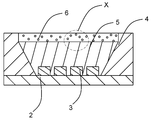
- FIG. 1 is an external perspective view of a light emitting device according to an embodiment of the present invention. It is sectional drawing when the light-emitting device shown in FIG. 1 is cut
- FIG. 1 is an external perspective view of a light emitting device according to an embodiment of the present invention.
- FIG. 2 is a cross-sectional view of the light emitting device shown in FIG. 1 taken along a plane indicated by an imaginary line.
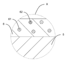
- FIG. 3 is an enlarged view of the light emitting device shown in FIG.
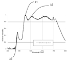
- FIG. 4 is a graph showing the spectrum of external radiation in the light emitting device according to the embodiment of the present invention.
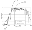
- FIG. 5 is a graph showing the spectrum of sunlight added to FIG.
- the light emitting device 1 includes a substrate 2, a plurality of light emitting elements 3, a frame 4, a sealing member 5, and a wavelength conversion member 6.
- the light emitting device 1 is surrounded by a substrate 2, a plurality of light emitting elements 3 provided on the substrate 2, a frame 4 provided on the substrate 2 so as to surround the plurality of light emitting elements 3, and a frame 4 In the inner space, the sealing member 5 filled with a part of the upper part of the space surrounded by the frame 4 and the part of the upper part of the inner space surrounded by the frame 4 And a wavelength conversion member 6 provided so as to be accommodated in the frame 4 along the upper surface of the member 5.
- the plurality of light emitting elements 3 are, for example, LEDs, and emit light toward the outside by recombination of electrons and holes in a pn junction using a semiconductor.
- the substrate 2 is an insulating substrate, and is made of, for example, a ceramic material such as alumina or mullite, or a glass ceramic material. Alternatively, it is composed of a composite material in which a plurality of materials among these materials are mixed. Further, as the substrate 2, a polymer resin in which metal oxide fine particles capable of adjusting the thermal expansion of the substrate 2 can be dispersed can be used.
- a wiring conductor that electrically conducts the inside and the outside of the substrate 2 is provided at least on the main surface of the substrate 2 or inside the substrate 2.
- the wiring conductor is made of, for example, a conductive material such as tungsten, molybdenum, manganese or copper.
- a metal paste obtained by adding an organic solvent to powder such as tungsten is printed on a ceramic green sheet to be the substrate 2 in a predetermined pattern, and a plurality of ceramic green sheets are laminated. It is obtained by baking.
- a plated layer of, for example, nickel or gold is formed on the surface of the wiring conductor to prevent oxidation.
- a metal reflective layer such as aluminum, silver, gold, copper, or platinum is spaced apart from the wiring conductor and the plating layer. You may form.
- the plurality of light emitting elements 3 are mounted on the main surface of the substrate 2.
- the plurality of light emitting elements 3 are electrically connected, for example, via a brazing material or solder on the plating layer deposited on the surface of the wiring conductor formed on the main surface of the substrate 2.
- the light emitting element 3 has a translucent substrate and a photosemiconductor layer formed on the translucent substrate.
- the light-transmissive substrate may be any substrate as long as the photosemiconductor layer can be grown using a chemical vapor deposition method such as a metal organic chemical vapor deposition method or a molecular beam epitaxial growth method.
- the translucent substrate for example, sapphire, gallium nitride, aluminum nitride, zinc oxide, zinc selenide, silicon carbide, silicone, zirconium diboride or the like can be used.
- the thickness of the translucent substrate is, for example, 50 ⁇ m or more and 1000 ⁇ m or less.
- the optical semiconductor layer is composed of a first semiconductor layer formed on the translucent substrate, a light emitting layer formed on the first semiconductor layer, and a second semiconductor layer formed on the light emitting layer.
- the first semiconductor layer, the light emitting layer and the second semiconductor layer may be, for example, a group III nitride semiconductor, a group III-V semiconductor such as gallium phosphorus or gallium arsenide, or a group III nitride such as gallium nitride, aluminum nitride or indium nitride An object semiconductor or the like can be used.
- the thickness of the first semiconductor layer is, for example, 1 ⁇ m to 5 ⁇ m
- the thickness of the light emitting layer is, for example, 25 nm to 150 nm
- the thickness of the second semiconductor layer is, for example, 50 nm to 600 nm.
- the light emitting element 3 configured in this manner can emit excitation light in a wavelength range of, for example, 340 nm or more and 450 nm or less.
- the frame 4 is made of, for example, a ceramic material such as aluminum oxide, titanium oxide, zirconium oxide or yttrium oxide, or a porous material, or a powder composed of a metal oxide such as aluminum oxide, titanium oxide, zirconium oxide or yttrium oxide It consists of the resin material which The frame 4 is connected to the main surface of the substrate 2 via, for example, a resin, a brazing material, or solder.
- the frame 4 is provided on the main surface of the substrate 2 so as to surround the light emitting element 3 at a distance from the light emitting element 3. Further, the frame 4 is formed so that the inclined inner wall surface spreads outward as the distance from the main surface of the substrate 2 is increased.
- the inner wall surface of the frame 4 functions as a reflection surface of the excitation light emitted from the light emitting element 3.
- the shape of the inner wall surface of the frame 4 is circular in plan view, the light emitted from the light emitting element 3 can be uniformly reflected outward by the reflection surface.
- the inclined inner wall surface of the frame 4 is made of, for example, a metal layer made of tungsten, molybdenum, manganese or the like on the inner peripheral surface of the frame 4 made of a sintered material, and nickel or gold covering the metal layer. You may form a plating layer.
- the plating layer has a function of reflecting the light emitted from the light emitting element 3.
- the inclination angle of the inner wall surface of the frame 4 is set to, for example, an angle of 55 degrees or more and 70 degrees or less with respect to the main surface of the substrate 2.
- a light transmissive sealing member 5 is filled in an inner space surrounded by the substrate 2 and the frame 4.
- the sealing member 5 seals the light emitting element 3 and extracts light emitted from the inside of the light emitting element 3 to the outside. Furthermore, it has a function of transmitting the light extracted to the outside of the light emitting element 3.
- the sealing member 5 is filled in the inner space surrounded by the substrate 2 and the frame 4 leaving a part of the space surrounded by the frame 4.
- the sealing member 5 is made of, for example, a translucent insulating resin such as silicone resin, acrylic resin or epoxy resin, or a translucent glass material.
- the refractive index of the sealing member 5 is set to, for example, 1.4 or more and 1.6 or less.
- the wavelength conversion member 6 is provided along the upper surface of the sealing member 5 in the upper part of the inner space surrounded by the substrate 2 and the frame 4.
- the wavelength conversion member 6 is formed to fit in the frame 4.
- the wavelength conversion member 6 has a function of converting the wavelength of the light emitted from the plurality of light emitting elements 3. That is, in the wavelength conversion member 6, the light emitted from the plurality of light emitting elements 3 enters the inside through the sealing member 5, and the fluorescent substance contained inside is excited by the light emitted from the light emitting element 3 While emitting fluorescence from a fluorescent substance, a part of the light from the light emitting element 3 is transmitted and emitted.
- the wavelength conversion member 6 is made of, for example, a translucent insulating resin such as fluorine resin, silicone resin, acrylic resin or epoxy resin, or a translucent glass material, and the insulating resin and the glass material contain a phosphor. It is contained. The phosphors are dispersed uniformly in the wavelength conversion member 6. The phosphors contained in the plurality of light emitting elements 3 and the wavelength conversion member 6 are selected so that the emission spectrum of the light emitted from the light emitting device 1 becomes the emission spectrum as shown in FIG.
- a translucent insulating resin such as fluorine resin, silicone resin, acrylic resin or epoxy resin, or a translucent glass material
- the phosphors are dispersed uniformly in the wavelength conversion member 6.
- the phosphors contained in the plurality of light emitting elements 3 and the wavelength conversion member 6 are selected so that the emission spectrum of the light emitted from the light emitting device 1 becomes the emission spectrum as shown in FIG.
- the light emitting device 1 uses the light emitting element 3 whose third peak wavelength ⁇ 3 of emission spectrum is 315 to 400 nm and emits blue fluorescence while having, for example, the first peak wavelength ⁇ 1 as a phosphor.
- a first phosphor 61 and a second phosphor 62 having a second peak wavelength ⁇ 2 and emitting blue-green fluorescence are used.
- a phosphor that emits green fluorescence, a phosphor that emits red fluorescence, and a phosphor that emits fluorescence in the near infrared region may be further used.
- the first fluorescent material 61 showing a blue color, BaMgAl 10 O 17: Eu, (Sr, Ca, Ba) 10 (PO 4) 6 Cl 2: Eu, (Sr, Ba) 10 (PO 4
- the second phosphor 62 which is 6 Cl 2 : Eu and shows a bluish green color is (Sr, Ba, Ca) 5 (PO 4 ) 3 Cl: Eu, Sr 4 Al 14 O 25 : Eu.
- the green phosphors are SrSi 2 (O, Cl) 2 N 2 : Eu, (Sr, Ba, Mg) 2 SiO 4 : Eu 2+ , ZnS: Cu, Al, Zn 2 SiO 4 : Mn.
- the phosphors exhibiting a red color are Y 2 O 2 S: Eu, Y 2 O 3 : Eu, SrCaClAlSiN 3 : Eu 2+ , CaAlSiN 3 : Eu, CaAlSi (ON) 3 : Eu.
- the phosphor exhibiting a near infrared region is 3Ga 5 O 12 : Cr.
- the phosphors such as the first phosphor 61 and the second phosphor 62
- the emitted fluorescence and the light emitted from the light emitting element 3 are combined.
- the light of the first peak wavelength is excited in the wavelength range of 400 to 500 nm with respect to the light emitted from the light emitting element 3, and the light of the second peak wavelength is excited in the wavelength range of 500 to 600 nm.
- the temperature of the first phosphor 61 and the temperature of the second phosphor 62 fluctuate, and the output of fluorescence at peak wavelengths emitted from the respective phosphors fluctuates. It is possible to reduce the variation in color of the light emitted from the light emitting device 1 caused by That is, even if the output of the fluorescence at the peak wavelength emitted from the phosphors of the first phosphor 61 or the second phosphor 62 fluctuates, the light emitted from the light emitting device 1 by the fluorescence emitted from the other phosphors The possibility of holding the color of light is high. Therefore, the light emitting device 1 according to the embodiment of the present invention reduces variation in color of light emitted from the light emitting device 1 caused by fluctuation of the intensity of fluorescence at the peak wavelength emitted from the phosphor. Can.
- the light emitting device 1 having the third peak wavelength ⁇ 3 at 315 to 400 nm By the light emitting device 1 having the third peak wavelength ⁇ 3 at 315 to 400 nm, light closer to sunlight is emitted in the ultraviolet region. This makes it possible to supply a light source suitable for plant growth and weatherability test.
- life-sustaining functions thermoregulation, growth promotion
- UVA region 315 to 400 nm
- light including near-ultraviolet light gives moderate stress to the grown object, and it can be expected that, for example, in the case of green and yellow vegetables, the vitamin C content increases. That is, the property as a food can be improved with respect to a plant.
- the light emitting device 1 according to the embodiment of the present invention can emit light with high color rendering that approximates the spectrum of sunlight. That is, the difference between the relative light intensity in the spectrum of sunlight and the relative light intensity in the emission spectrum of the light emitting device 1 according to the embodiment of the present invention can be reduced, and the light emitting device 1 approximated to sunlight is manufactured. be able to.
- the spectral distribution (integrated value of emission spectrum, ie, light energy) in the wavelength range of 315 to 400 nm is 20% or more of the spectral distribution in the wavelength range of 300 to 950 nm as a whole. 60% or less.
- the light emitting device 1 can emit light close to the spectrum of sunlight in the ultraviolet and violet regions, and can emit light with small color variation. That is, the light emitting device 1 can emit light having an emission spectrum over the wavelength range of near ultraviolet and visible light, and part of the light intensity of the light emitting element 3 or the phosphor, that is, the relative light shown in the vertical axis of FIG. It is possible to reduce the color variation of the ultraviolet and violet regions emitted from the light emitting device 1 caused by the intensity variation.
- the light intensity difference between the maximum value and the minimum value of the emission spectrum in the wavelength range of 430 to 700 nm in the emission spectrum may be 20% or less.
- the light emitting device 1 can reduce the possibility that the variation in color of the light emitted from blue to yellow becomes large.
- the maximum peak of the emission spectrum is in the visible light range of 400 to 500 nm.
- the wavelength having this maximum peak is the first peak wavelength ⁇ 1.
- the maximum peak wavelength refers to the wavelength with the highest relative light intensity in the spectrum between 300 and 950 nm.
- FIG. 4 and FIG. 5 show an example of a fluorescence spectrum including the first phosphor 61 and the second phosphor 62 of the phosphors used in the light emitting device 1 of the present embodiment. In each spectrum, it is the spectrum shown by the relative light intensity which makes 1 the highest light intensity.
- the emission spectra and the respective fluorescence spectra shown in FIGS. 4 to 5 indicate relative light intensities based on the measured values measured.
- the light intensity below the UVA region may be 30% or less of the peak intensity of the UVA region (315 to 400 nm). By this, it can be reduced that the light in the ultraviolet region becomes too strong.
- the light emitting device 1 is used, for example, in a configuration in which a plurality of the light emitting devices 1 are arranged in a lighting device used indoors such as in a building or a house.
- a lighting device used indoors such as in a building or a house.
- a lighting device in a living space it is possible to construct a lighting environment in which sunlight is emitted even indoors.
- it is used as an illuminating device for visual inspections, such as a painted article, for example, a passenger car the inspection environment where sunlight was irradiated can be built even indoors.
- the embodiments of the lighting device 10 including a plurality of light emitting devices may have a similar emission spectrum. That is, by combining a plurality of light emitting devices having the light emitting element 3, the lighting device 10 has a first peak wavelength in the wavelength range of 400 to 500 nm and a wavelength of 500 to 600 nm as the light emitting device 1 described above. It has a second peak wavelength in the region.
- the illumination device 10 By having the third peak wavelength ⁇ 3 at 315 to 400 nm, the illumination device 10 emits light closer to sunlight in the ultraviolet region. This makes it possible to supply a light source suitable for plant growth and weatherability test.
- the life-sustaining function thermoregulation, growth promotion
- light including near-ultraviolet light gives moderate stress to the grown object, and it can be expected that, for example, in the case of green and yellow vegetables, the vitamin C content increases. That is, the property as a food can be improved with respect to a plant.
- the illumination device 10 has a spectral distribution (integrated value of emission spectrum, ie, light energy) in a wavelength range of 315 to 400 nm of 20% or more of the spectral distribution in a wavelength range of 300 to 950 nm in total. 60% or less.
- a spectral distribution integrated value of emission spectrum, ie, light energy
- the lighting device 10 can emit light that approximates the spectrum of sunlight and can emit light with small color variation.
- the wavelength having this maximum peak is the first peak wavelength ⁇ 1.
- the maximum peak wavelength refers to the wavelength with the highest relative light intensity in the spectrum between 300 and 950 nm.
- the light intensity difference between the maximum value and the minimum value of the emission spectrum in the wavelength region of 430 to 700 nm may be 20% or less.
- the light intensity below the UVA region may be 30% or less of the peak intensity of the UVA region (315 to 400 nm). By this, it can be reduced that the light in the ultraviolet region becomes too strong.
- FIG. 6 is an external perspective view of a lighting apparatus including the light emitting device according to the present embodiment
- FIG. 7 is an exploded perspective view of the lighting apparatus shown in FIG.
- FIG. 8 is a perspective view showing a state in which the translucent substrate is removed from the housing of the lighting device shown in FIG.
- the long wiring board 12 and the long light transmitting substrate 13 supported by the housing 11 and closing the opening of the housing 11 are provided.
- the spectrum in the light-emitting device 1 was demonstrated, the spectrum in the illuminating device 10 may become as mentioned above.
- the light emitting element 3 similarly has the third peak wavelength ⁇ 3 at 315 to 400 nm, and can be reproduced by appropriately changing the type of phosphor.
- the housing 11 has a function of holding the light transmitting substrate 13 and a function of dissipating the heat generated by the light emitting device 1 to the outside.
- the housing 11 is made of, for example, metal such as aluminum, copper or stainless steel, plastic or resin.
- the housing 11 has a longitudinally extending bottom portion 21a and a pair of longitudinally extending support portions 21b erected from both end portions in the width direction of the bottom portion 21a, and is open at both upper and longitudinal directions. It comprises an elongated main body portion 21 and two lid portions 22 closing the openings on one side and the other side in the longitudinal direction of the main body portion 21 respectively.
- each support portion 21b holding portions are provided in which recesses for holding the light transmitting substrate 13 along the longitudinal direction are formed to face each other.
- the housing 11 is set to have a length in the longitudinal direction of, for example, 100 mm or more and 2000 mm or less.
- the wiring substrate 12 is fixed to the bottom of the housing 11.
- the wiring board 12 for example, a printed board such as a rigid board, a flexible board, or a rigid flexible board is used.
- the wiring pattern of the wiring substrate 12 and the wiring pattern of the substrate 2 in the light emitting device 1 are electrically connected via solder or a conductive adhesive. Then, a signal from the wiring substrate 12 is transmitted to the light emitting element 3 through the substrate 2 and the light emitting element 3 emits light. Power is supplied to the wiring board 12 from a power supply provided outside via a wiring.
- the translucent substrate 13 is made of a material through which light emitted from the light emitting device 1 is transmitted, and is made of, for example, a light transmitting material such as acrylic resin or glass.
- the translucent substrate 13 is a rectangular plate, and the length in the longitudinal direction is set to, for example, 98 mm or more and 1998 mm or less.
- the translucent substrate 13 is inserted into the recess formed in each of the support portions 21 b from the opening on one side or the other side in the longitudinal direction of the main body portion 21 and is slid along the longitudinal direction.
- the light emitting device 1 is supported by the pair of support portions 21 b at a position away from the light emitting device 1.
- the illumination device 10 is configured by closing the opening on the one side and the other side in the longitudinal direction of the main body 21 with the lid 22.
- said illuminating device 10 is an illuminating device of the line emission which arranged the several light-emitting devices 1 in linear form, the surface which arranged not only this but several light-emitting devices 1 in the matrix form or the zigzag grid shape It may be a light emitting illumination device.
- the light emitting device 1 emits, as the phosphors contained in one wavelength conversion member 6, the first phosphor 61 that emits blue fluorescence, and the blue fluorescence that emits blue fluorescence.
- the first phosphor 61 that emits blue fluorescence
- the blue fluorescence that emits blue fluorescence.
- two phosphors 62 a phosphor emitting green fluorescence, a phosphor emitting red fluorescence and a phosphor emitting near-infrared fluorescence are included, five types of phosphors are included. Not limited to this, two types of wavelength conversion members may be provided.
- wavelength conversion members When two types of wavelength conversion members are provided, they are used as the first wavelength conversion member, and different phosphors are dispersed in the second wavelength conversion member, or the phosphors are dispersed in different combinations to form one light emitting device. These two wavelength conversion members may be provided to mix the light emitted through the respective wavelength conversion members. This makes it easy to control the color rendering of the emitted light.
- the light emitting device 1 shown in FIG. 1 and FIG. 2 was actually produced and evaluated for color rendering.
- the plurality of light emitting elements 3 for emitting excitation light is a light emitting element made of gallium nitride that has a plurality of peak wavelengths in a wavelength band of 315 to 400 nm and emits light having a half width of 15 nm.
- the first phosphor 61 is (Sr, Ca, Ba) 10 (PO 4 ) 6 Cl 2 : Eu
- the second phosphor 62 exhibiting blue-green color is Sr 4 Al 14 O 25 : Eu
- the green-emitting phosphor is SrSi 2 (O, Cl) 2 N 2 : Eu.
- the phosphor exhibiting a red color is CaAlSi (ON) 3 : Eu.
- the phosphor exhibiting a near infrared region is 3Ga 5 O 12 : Cr.
- the emission spectrum of the manufactured light emitting device 1 is the emission spectrum shown in FIG.
Landscapes
- Led Device Packages (AREA)
- Cultivation Of Plants (AREA)
- Fastening Of Light Sources Or Lamp Holders (AREA)
Abstract
本発明の一実施形態に係る発光装置は、発光素子と、第1蛍光体と、第2蛍光体とを備えている。第1蛍光体は、発光素子から発光される光に対して、外部に放射される光の発光スペクトルのうち400~500nmの波長領域に第1ピーク波長を有する光を励起する。第2蛍光体は、発光素子から発光される光に対して、前記発光スペクトルのうち500~600nmの波長領域に第2ピーク波長を有する光を励起する。発光素子3は、前記発光スペクトルのうち315~400nmの波長領域に第3ピーク波長を有する。
Description
本発明は、LED等を使用した発光装置および照明装置に関する。
近年、蛍光灯や電球に代わってLED(Light Emitting Diode)などの半導体発光素子を光源とする照明装置が用いられている。また、例えば、家電製品や乗用自動車などの塗装面の外観検査用光源としても発光素子を光源とする照明装置が用いられている。
半導体発光素子は、放射光の波長帯域が狭く、単一色の光しか放射できない。照明光を白色光としたい場合は、放射光の波長帯域が異なる複数の半導体発光素子を準備し、複数の放射光の混色によって白色光を実現している。または、同一波長の励起光によって波長帯域の異なる蛍光を発光する複数の蛍光体を準備し、半導体発光素子からの放射光と、半導体発光素子からの放射光によって励起されて発光する複数の蛍光の混色によって白色光を実現している。このような混色の手法を用いれば、白色光以外にも目的に応じたスペクトルを有する光源を作製することができる(特開2015-126160号公報参照)。
しかしながら、特開2015-126160号公報に開示された技術は、白色光を照射したときの照射面における外観と、太陽光のもとで見たときの照射面における外観とでは、見え方が異なる場合があった。外観検査において、実際の太陽光のもとで見るときの外観の使用状態と差が出てしまう場合があった。
本発明の一実施形態に係る発光装置は、発光素子と、第1蛍光体と、第2蛍光体とを備えている。第1蛍光体は、発光素子から発光される光に対して、外部に放射される光の発光スペクトルのうち400~500nmの波長領域に第1ピーク波長を有する光を励起する。第2蛍光体は、発光素子から発光される光に対して、発光スペクトルのうち500~600nmの波長領域に第2ピーク波長を有する光を励起する。発光素子は、発光スペクトルのうち315~400nmの波長領域に第3ピーク波長を有している。
本発明の一実施形態に係る照明装置は、上記の発光装置を少なくとも1つ備えることを特徴とする。
本発明の一実施形態に係る照明装置は、発光素子を有する複数の発光装置を備えている。複数の発光装置から放射された光の発光スペクトルのうち、400~500nmの波長領域に第1ピーク波長を有し、500~600nmの波長領域に第2ピーク波長を有し、315~400nmの波長領域に第3ピーク波長を有している。第3ピーク波長の光強度は、全波長領域の最大ピーク波長の光強度の20%以上60%以下であり、315nm以下の波長領域における光強度は第3ピーク波長の光強度の30%以下である。
以下に本発明の実施形態に係る発光装置および照明装置の実施形態を、図面を参照しながら説明する。
<発光装置の構成>
図1は、本発明の一実施形態に係る発光装置の外観斜視図である。図2は、図1に示す発光装置を仮想線で示す平面で切断したときの断面図である。図3は、図2に示す発光装置の拡大図である。図4は、本発明の実施形態の発光装置における外部放射光のスペクトルを示すグラフである。図5は、図4に太陽光のスペクトルを加えて示すグラフである。これらの図において、発光装置1は、基板2と、複数の発光素子3と、枠体4と、封止部材5と、波長変換部材6とを備えている。
図1は、本発明の一実施形態に係る発光装置の外観斜視図である。図2は、図1に示す発光装置を仮想線で示す平面で切断したときの断面図である。図3は、図2に示す発光装置の拡大図である。図4は、本発明の実施形態の発光装置における外部放射光のスペクトルを示すグラフである。図5は、図4に太陽光のスペクトルを加えて示すグラフである。これらの図において、発光装置1は、基板2と、複数の発光素子3と、枠体4と、封止部材5と、波長変換部材6とを備えている。
発光装置1は、基板2と、基板2上に設けられた複数の発光素子3と、基板2上に複数の発光素子3を取り囲むように設けられた枠体4と、枠体4で囲まれた内側の空間内に、枠体4で囲まれる空間の上部の一部を残して充填された封止部材5と、枠体4で囲まれた内側の空間の上部の一部に、封止部材5の上面に沿って枠体4内に収まるように設けられた波長変換部材6と、を備えている。なお、複数の発光素子3は、例えば、LEDであって、半導体を用いたpn接合中の電子と正孔が再結合することによって、外部に向かって光を放出する。
基板2は、絶縁性の基板であって、例えば、アルミナまたはムライト等のセラミック材料、あるいはガラスセラミック材料等からなる。または、これらの材料のうち複数の材料を混合した複合系材料から成る。また、基板2は、基板2の熱膨張を調整することが可能な金属酸化物微粒子を分散させた高分子樹脂を用いることができる。
少なくとも基板2の主面または基板2の内部には、基板2の内外を電気的に導通する配線導体が設けられている。配線導体は、例えば、タングステン、モリブデン、マンガンまたは銅等の導電材料からなる。基板2がセラミック材料から成る場合は、例えば、タングステン等の粉末に有機溶剤を添加して得た金属ペーストを、基板2となるセラミックグリーンシートに所定パターンで印刷し、複数のセラミックグリーンシートを積層して、焼成することにより得られる。なお、配線導体の表面には、酸化防止のために、例えば、ニッケルまたは金等のめっき層が形成されている。また、基板2の上面には、基板2上方に効率良く光を反射させるために、配線導体およびめっき層と間隔を空けて、例えば、アルミニウム、銀、金、銅またはプラチナ等の金属反射層を形成してもよい。
複数の発光素子3は、基板2の主面上に実装される。複数の発光素子3は、基板2主面上に形成される配線導体の表面に被着するめっき層上に、例えば、ろう材または半田を介して電気的に接続される。発光素子3は、透光性基体と、透光性基体上に形成される光半導体層とを有している。透光性基体は、有機金属気相成長法または分子線エピタキシャル成長法等の化学気相成長法を用いて、光半導体層を成長させることが可能なものであればよい。透光性基体に用いられる材料としては、例えば、サファイア、窒化ガリウム、窒化アルミニウム、酸化亜鉛、セレン化亜鉛、シリコンカーバイド、シリコーンまたは二ホウ化ジルコニウム等を用いることができる。なお、透光性基体の厚みは、例えば50μm以上1000μm以下である。
光半導体層は、透光性基体上に形成される第1半導体層と、第1半導体層上に形成される発光層と、発光層上に形成される第2半導体層とから構成されている。第1半導体層、発光層および第2半導体層は、例えば、III族窒化物半導体、ガリウム燐またはガリウムヒ素等のIII-V族半導体、あるいは、窒化ガリウム、窒化アルミニウムまたは窒化インジウム等のIII族窒化物半導体等を用いることができる。なお、第1半導体層の厚みは、例えば1μm以上5μm以下であって、発光層の厚みは、例えば25nm以上150nm以下であって、第2半導体層の厚みは、例えば50nm以上600nm以下である。また、このように構成された発光素子3は、例えば340nm以上450nm以下の波長範囲の励起光を発することができる。
枠体4は、例えば、酸化アルミニウム、酸化チタン、酸化ジルコニウムまたは酸化イットリウム等のセラミック材料、あるいは多孔質材料、あるいは酸化アルミニウム、酸化チタン、酸化ジルコニウムまたは酸化イットリウム等の金属酸化物からなる粉末を混合させた樹脂材料から成る。枠体4は、基板2の主面に、例えば樹脂、ろう材または半田等を介して接続されている。枠体4は、発光素子3と間隔を空けて、発光素子3を取り囲むように基板2の主面上に設けられている。また、枠体4は、傾斜する内壁面が、基板2の主面から遠ざかるに従い、外方に向かって広がるように形成されている。そして、枠体4の内壁面が、発光素子3から発せられる励起光の反射面として機能する。なお、平面視して、枠体4の内壁面の形状を円形とすると、発光素子3が放射する光を一様に反射面にて外方に向かって反射させることができる。
また、枠体4の傾斜する内壁面は、例えば、焼結材料からなる枠体4の内周面にタングステン、モリブデン、マンガン等から成る金属層と、金属層を被覆するニッケルまたは金等から成るめっき層を形成してもよい。このめっき層は、発光素子3の発する光を反射させる機能を有する。なお、枠体4の内壁面の傾斜角度は、基板2の主面に対して例えば55度以上70度以下の角度に設定されている。
基板2および枠体4で囲まれる内側の空間には、光透過性の封止部材5が充填されている。封止部材5は、発光素子3を封止するとともに、発光素子3の内部から発せられる光を外部に光を取り出す。さらに、発光素子3の外部に取り出された光が透過する機能を備えている。封止部材5は、基板2および枠体4で囲まれる内側の空間内に、枠体4で囲まれる空間の一部を残して充填されている。封止部材5は、例えば、シリコーン樹脂、アクリル樹脂またはエポキシ樹脂等の透光性の絶縁樹脂や透光性のガラス材料が用いられる。封止部材5の屈折率は、例えば1.4以上1.6以下に設定されている。
波長変換部材6は、基板2および枠体4で囲まれた内側の空間の上部に、封止部材5の上面に沿って設けられている。波長変換部材6は、枠体4内に収まるように形成されている。波長変換部材6は、複数の発光素子3の発する光の波長を変換する機能を有している。すなわち、波長変換部材6は、複数の発光素子3から発せられる光が封止部材5を介して内部に入射して、内部に含有される蛍光体が発光素子3から発せられる光によって励起されて、蛍光体からの蛍光を発するとともに、発光素子3からの光の一部を透過させて放射するものである。波長変換部材6は、例えば、フッ素樹脂、シリコーン樹脂、アクリル樹脂またはエポキシ樹脂等の透光性の絶縁樹脂、または透光性のガラス材料からなり、その絶縁樹脂、ガラス材料中に、蛍光体が含有されている。蛍光体は、波長変換部材6中に均一に分散するようにしている。複数の発光素子3および波長変換部材6中に含有される蛍光体としては、発光装置1から発せられる光の発光スペクトルが、図4に示すような発光スペクトルとなるように選ばれる。
本発明の実施形態の発光装置1では、発光スペクトルの第3ピーク波長λ3が315~400nmである発光素子3を用い、蛍光体として、例えば、第1ピーク波長λ1を有するとともに青色の蛍光を発する第1蛍光体61と、第2ピーク波長λ2を有するとともに青緑色の蛍光を発する第2蛍光体62と、を用いている。この他にも、緑色の蛍光を発する蛍光体と、赤色の蛍光を発する蛍光体と、近赤外領域の蛍光を発する蛍光体とをさらに用いてもよい。
各蛍光体は例えば、青色を示す第1蛍光体61は、BaMgAl10O17:Eu、(Sr,Ca,Ba)10(PO4)6Cl2:Eu,(Sr,Ba)10(PO4)6Cl2:Euであり、青緑色を示す第2蛍光体62は、(Sr,Ba,Ca)5(PO4)3Cl:Eu,Sr4Al14O25:Euである。緑色を示す蛍光体は、SrSi2(O,Cl)2N2:Eu、(Sr,Ba,Mg)2SiO4:Eu2+、ZnS:Cu,Al、Zn2SiO4:Mnである。赤色を示す蛍光体としては、Y2O2S:Eu、Y2O3:Eu、SrCaClAlSiN3:Eu2+、CaAlSiN3:Eu、CaAlSi(ON)3:Euである。近赤外領域を示す蛍光体は、3Ga5O12:Crである。
本発明の実施形態に係る発光装置1は、外部に放射される光の発光スペクトルの波長領域となる300~950nmの波長領域において、第1蛍光体61、第2蛍光体62等の蛍光体から放射される蛍光と、発光素子3から放射される光を合成する。このことにより、発光素子3から発光される光に対して400~500nmの波長領域に第1ピーク波長の光が励起され、500~600nmの波長領域に第2ピーク波長の光が励起される。
このことによって、本発明の実施形態に係る発光装置1は、第1蛍光体61、第2蛍光体62の温度が変動し、それぞれの蛍光体から放射される、ピーク波長における蛍光の出力が変動することによって生じる、発光装置1から放射される光の色のバラツキを小さくすることができる。すなわち、第1蛍光体61または第2蛍光体62の蛍光体から放射される、ピーク波長における蛍光の出力が変動する場合であっても、他の蛍光体から放射される蛍光によって発光装置1からの光の色を保持できる可能性が高くなる。よって、本発明の実施形態に係る発光装置1は、蛍光体から放射される、ピーク波長における蛍光の強度が変動することによって生じる、発光装置1から放射される光の色のバラツキを低減することができる。
発光装置1が、315~400nmにおける第3ピーク波長λ3を有することによって、紫外領域においてより太陽光に近い光が照射される。このことによって、植物育成や耐候性試験用に適した光源を供給することが可能となる。また、屋内飼育用の生物の育成において、爬虫類および両生類等の陸上生物に、315~400nm(UVA領域)の光を照射することで、生命維持機能(体温調節、成長促進)を向上させることができる。また植物栽培においては、近紫外線を含む光が育成対象物に対して程よいストレスを与え、例えば緑黄色野菜などではビタミンC含有量が増加することが期待できる。すなわち、植物に対して、食物としての特性を向上させることができる。
さらに、本発明の実施形態に係る発光装置1は、太陽光のスペクトルに近似する、演色性の高い光を放射することができる。即ち、太陽光のスペクトルにおける相対光強度と、本発明の実施形態に係る発光装置1の発光スペクトルにおける相対光強度との差を小さくすることができ、太陽光に近似した発光装置1を作製することができる。
本発明の他の実施形態に係る発光装置1は、315~400nmの波長領域における分光分布(発光スペクトルの積分値、すなわち光エネルギー)は、全体300~950nmの波長領域における分光分布の20%以上60%以下である。この結果、発光装置1は、紫外および紫領域において、太陽光のスペクトルに近似する光を放射することができるとともに、色のバラツキが小さい光を放射できる。すなわち、発光装置1は、近紫外および可視光の波長領域にわたる発光スペクトルを有する光を放射できるとともに、発光素子3や蛍光体における一部の光強度、すなわち、図4の縦軸に示す相対光強度が変動することによって生じる、発光装置1から放射される紫外および紫領域の色のバラツキを低減させることができる。
また、本発明の実施形態に係る発光装置1は、発光スペクトルのうち430~700nmの波長領域における発光スペクトルの最大値と最小値の光強度差が20%以下であってもよい。このことによって、発光装置1は、青色から黄色にかけて放射する光の色のバラツキが大きくなる可能性を低減できる。
また、可視光域の400~500nmに発光スペクトルの最大ピークがある。この最大ピークを有する波長が第1ピーク波長λ1である。最大ピーク波長とは、300~950nmの間のスペクトルのうち、最も相対光強度の高い波長のことをいう。最大ピーク波長が400~500nmに位置していることにより、太陽光スペクトルに近似する光を放射することができ、生物の飼育や植物の育成に適した光を供給することが可能となる。
図4および図5は、本実施形態の発光装置1で用いられる蛍光体の第1蛍光体61および第2蛍光体62を含む蛍光スペクトルの一例を示している。それぞれのスペクトルにおいて、最も高い光強度を1とする相対光強度で示したスペクトルである。なお、図4~5に示す発光スペクトルおよび各蛍光スペクトルは、測定された実測値に基づき、相対光強度を示している。
また、UVA領域以下、つまり315nm以下の光強度はUVA領域(315~400nm)のピーク強度の30%以下であってもよい。このことによって、紫外域の光が強くなりすぎることを低減させることができる。
本発明の実施形態の発光装置1は、建物内、家屋内などの屋内で用いられる照明装置において、例えば、複数個配列して構成される形態などで利用される。例えば、居住空間の照明装置であれば、屋内であっても太陽光が照射されたような照明環境を構築することができる。また、塗装された物品、例えば乗用自動車などの外観検査用の照明装置として用いれば、屋内であっても太陽光が照射されたような検査環境を構築することができる。屋内にいても太陽光に近い光が照射されることによって、太陽光の下で見える色に近い見え方にすること(演色性の向上)ができ、色の検査を行なう場合に、より正確に検査することができる。また、屋内飼育用の生物の育成において、爬虫類および両生類等の陸上生物に、315~400nm(UVA領域)の光を照射することで、生命維持機能(体温調節、成長促進)を向上させることができる。
なお、これまで発光装置1の実施形態について説明してきたが、複数の発光装置を備えた照明装置10の実施形態として、同様の発光スペクトルを有していてもよい。すなわち、発光素子3を有する複数の発光装置を組み合わせることにより、上述した発光装置1と同様に、照明装置10として、400~500nmの波長領域に第1ピーク波長を有し、500~600nmの波長領域に第2ピーク波長を有している。
照明装置10が、315~400nmにおける第3ピーク波長λ3を有することによって、紫外領域においてより太陽光に近い光が照射される。このことによって、植物育成や耐候性試験用に適した光源を供給することが可能となる。また、屋内飼育用の生物の育成において、爬虫類および両生類等の陸上生物に、315~400nm(UVA領域)の光を照射することで、生命維持機能(体温調節、成長促進)を向上させることができる。また植物栽培においては、近紫外線を含む光が育成対象物に対して程よいストレスを与え、例えば緑黄色野菜などではビタミンC含有量が増加することが期待できる。すなわち、植物に対して、食物としての特性を向上させることができる。
本発明の他の実施形態に係る照明装置10は、315~400nmの波長領域における分光分布(発光スペクトルの積分値、すなわち光エネルギー)は、全体300~950nmの波長領域における分光分布の20%以上60%以下である。この結果、照明装置10は、紫外および紫領域において、太陽光のスペクトルに近似する光を放射することができるとともに、色のバラツキが小さい光を放射できる。
また、可視光域の400~500nmに最大ピークがある。この最大ピークを有する波長が第1ピーク波長λ1である。最大ピーク波長とは、300~950nmの間のスペクトルのうち、最も相対光強度の高い波長のことをいう。最大ピーク波長が400~500nmに位置していることにより、太陽光スペクトルに近似する光を放射することができ、生物の飼育や植物の育成に適した光を供給することが可能となる。また、430~700nmの波長領域における発光スペクトルの最大値と最小値の光強度差が20%以下であってもよい。このことによって、照明装置10は、青色から黄色にかけて放射する光の色のバラツキが大きくなる可能性を低減できる。
また、UVA領域以下、つまり315nm以下の光強度はUVA領域(315~400nm)のピーク強度の30%以下であってもよい。このことによって、紫外域の光が強くなりすぎることを低減させることができる。
以下に添付図面を参照して、本実施形態に係る発光装置1を備える照明装置の一例を説明する。
<照明装置の構成>
図6は、本実施形態に係る発光装置を備える照明装置の外観斜視図であり、図7は、図6に示す照明装置の分解斜視図である。図8は、図6に示す照明装置の筐体から透光性基板を取り外した状態を示す斜視図である。
図6は、本実施形態に係る発光装置を備える照明装置の外観斜視図であり、図7は、図6に示す照明装置の分解斜視図である。図8は、図6に示す照明装置の筐体から透光性基板を取り外した状態を示す斜視図である。
照明装置10は、上方に開口している長尺の筐体11と、筐体11内に長手方向に沿ってライン状に複数個配列された発光装置1と、複数の発光装置1が実装される長尺の配線基板12と、筐体11によって支持され、筐体11の開口を閉塞する長尺の透光性基板13とを備えている。
なお、発光装置1におけるスペクトルについて説明したが、照明装置10におけるスペクトルが上述のようになっていてもよい。この場合には、発光素子3は同じく315~400nmに第3ピーク波長λ3を有するものであり、蛍光体の種類を適宜変更して、再現することができる。
筐体11は、透光性基板13を保持する機能と、発光装置1の発する熱を外部に放散させる機能とを有している。筐体11は、例えば、アルミニウム、銅またはステンレス等の金属、プラスチックまたは樹脂等から構成される。筐体11は、長手方向に延びる底部21a、および底部21aの幅方向の両端部から立設し、長手方向に延びる一対の支持部21bを有し、上方および長手方向の両側で開口している長尺の本体部21と、本体部21における長手方向一方側および他方側の開口をそれぞれ閉塞する2つの蓋部22とから成っている。各支持部21bの筐体11の内側における上部には、長手方向に沿って透光性基板13を保持するための凹所が互いに対向するように形成された保持部が設けられている。筐体11は、長手方向の長さが、例えば、100mm以上2000mm以下に設定されている。
配線基板12は、筐体11内の底面に固定される。配線基板12は、例えば、リジッド基板、フレキシブル基板またはリジッドフレキシブル基板等のプリント基板が用いられる。配線基板12の配線パターンと発光装置1における基板2の配線パターンとが、半田または導電性接着剤を介して電気的に接続される。そして、配線基板12からの信号が基板2を介して発光素子3に伝わり、発光素子3が発光する。なお、配線基板12には、外部に設けられた電源から配線を介して電力が供給される。
透光性基板13は、発光装置1から発せられる光が透過する材料からなり、例えば、アクリル樹脂またはガラス等の光透過性材料から構成される。透光性基板13は、矩形状の板体であって、長手方向の長さが、例えば、98mm以上1998mm以下に設定されている。透光性基板13は、本体部21における長手方向一方側または他方側の開口から、上述の各支持部21bに形成されている凹所内に挿し込み、長手方向に沿ってスライドさせることにより、複数の発光装置1から離れた位置で、一対の支持部21bによって支持される。そして、本体部21における長手方向一方側および他方側の開口を蓋部22で閉塞することにより、照明装置10は構成される。
なお、上記の照明装置10は、複数の発光装置1を直線状に配列した線発光の照明装置であるが、これに限らず複数の発光装置1をマトリクス状や千鳥格子状に配列した面発光の照明装置であってもよい。
本発明の実施形態における発光装置1は、1つの波長変換部材6中に含まれる蛍光体として、上記のように、青色の蛍光を放射する第1蛍光体61、青緑色の蛍光を放射する第2蛍光体62、緑色の蛍光を放射する蛍光体、赤色の蛍光を放射する蛍光体および近赤外領域の蛍光を放射する蛍光体からなる5種類の蛍光体を含む構成としたが、これに限らず、2種類の波長変換部材を備えるようにしてもよい。2種類の波長変換部材を備える場合には、第1の波長変換部材とし、第2の波長変換部材とに異なる蛍光体を分散あるいは、異なる組合せで蛍光体を分散させて、1つの発光装置にこれら2つの波長変換部材を設け、それぞれの波長変換部材を通過して出射される光を混合するようにしてもよい。このようにすることで、放射される光の演色性をコントロールしやすくできる。
図1、図2に示す発光装置1を実際に作製し、演色性について評価した。励起光を放射する複数の発光素子3は、ピーク波長が315~400nmの波長帯域に複数あり、半値幅が15nmの光を発する、窒化ガリウムから成る発光素子である。
第1蛍光体61は、(Sr,Ca,Ba)10(PO4)6Cl2:Euであり、青緑色を示す第2蛍光体62は、Sr4Al14O25:Euである。緑色を示す蛍光体は、SrSi2(O,Cl)2N2:Euである。赤色を示す蛍光体は、CaAlSi(ON)3:Euである。近赤外領域を示す蛍光体は、3Ga5O12:Crである。
作製した発光装置1の発光スペクトルは、図4に示した発光スペクトルである。
なお、本発明は上述の実施形態の例に限定されるものではなく、数値などの種々の変形は可能である。本実施形態における特徴部の種々の組み合わせは上述の実施形態の例に限定されるものではない。
1 発光装置
10 照明装置
11 筐体
12 配線基板
13 透光性基板
2 基板
21 本体部
21a 底部
21b 支持部
22 蓋部
3 発光素子
4 枠体
5 封止部材
6 波長変換部材
61 第1蛍光体
62 第2蛍光体
λ1 第1ピーク波長
λ2 第2ピーク波長
λ3 第3ピーク波長
10 照明装置
11 筐体
12 配線基板
13 透光性基板
2 基板
21 本体部
21a 底部
21b 支持部
22 蓋部
3 発光素子
4 枠体
5 封止部材
6 波長変換部材
61 第1蛍光体
62 第2蛍光体
λ1 第1ピーク波長
λ2 第2ピーク波長
λ3 第3ピーク波長
Claims (10)
- 発光素子と、
前記発光素子から発光される光に対して、外部に放射される光の発光スペクトルのうち400~500nmの波長領域に第1ピーク波長を有する光を励起する第1蛍光体と、
前記発光素子から発光される光に対して、前記発光スペクトルのうち500~600nmの波長領域に第2ピーク波長を有する光を励起する第2蛍光体と、
を備えており、
前記発光素子は、前記発光スペクトルのうち315~400nmの波長領域に第3ピーク波長を有することを特徴とする発光装置。 - 前記第1ピーク波長が、前記発光スペクトルのうち最大ピーク波長であることを特徴とする請求項1に記載の発光装置。
- 第3ピーク波長の光強度は、前記発光スペクトルの全波長領域の最大ピーク波長の光強度の20%以上60%以下であることを特徴とする請求項1または2に記載の発光装置。
- 315nm以下の波長領域における光強度は前記第3ピーク波長の光強度の30%以下であることを特徴とする請求項1~3のいずれか1つに記載の発光装置。
- 前記発光素子を複数備えたことを特徴とする請求項1~4のいずれか1つに記載の発光装置。
- 請求項1~5のいずれか1つに記載の発光装置を少なくとも1つ備えたことを特徴とする照明装置。
- 発光素子を有する複数の発光装置を備えており、
前記複数の発光装置から放射された光の発光スペクトルのうち、400~500nmの波長領域に第1ピーク波長を有し、500~600nmの波長領域に第2ピーク波長に有し、315~400nmの波長領域に第3ピーク波長を有していることを特徴とする照明装置。 - 前記第1ピーク波長が、前記発光スペクトルのうち最大ピーク波長であることを特徴とする請求項7に記載の照明装置。
- 第3ピーク波長の光強度は、前記発光スペクトルの全波長領域の最大ピーク波長の光強度の20%以上60%以下であることを特徴とする請求項7または8に記載の照明装置。
- 315nm以下の波長領域における光強度は前記第3ピーク波長の光強度の30%以下であることを特徴とする請求項7~9のいずれか1つに記載の照明装置。
Priority Applications (4)
| Application Number | Priority Date | Filing Date | Title |
|---|---|---|---|
| EP18901904.5A EP3748702A4 (en) | 2018-01-29 | 2018-12-20 | LIGHT EMITTING DEVICE AND LIGHTING DEVICE |
| US16/965,874 US20210043809A1 (en) | 2018-01-29 | 2018-12-20 | Light-emitting device and illumination apparatus |
| JP2019567923A JPWO2019146327A1 (ja) | 2018-01-29 | 2018-12-20 | 発光装置および照明装置 |
| JP2022045243A JP2022103159A (ja) | 2018-01-29 | 2022-03-22 | 発光装置、照明装置および生物育成用の照明装置 |
Applications Claiming Priority (2)
| Application Number | Priority Date | Filing Date | Title |
|---|---|---|---|
| JP2018-012612 | 2018-01-29 | ||
| JP2018012612 | 2018-01-29 |
Publications (1)
| Publication Number | Publication Date |
|---|---|
| WO2019146327A1 true WO2019146327A1 (ja) | 2019-08-01 |
Family
ID=67395373
Family Applications (1)
| Application Number | Title | Priority Date | Filing Date |
|---|---|---|---|
| PCT/JP2018/046998 Ceased WO2019146327A1 (ja) | 2018-01-29 | 2018-12-20 | 発光装置および照明装置 |
Country Status (4)
| Country | Link |
|---|---|
| US (1) | US20210043809A1 (ja) |
| EP (1) | EP3748702A4 (ja) |
| JP (2) | JPWO2019146327A1 (ja) |
| WO (1) | WO2019146327A1 (ja) |
Cited By (1)
| Publication number | Priority date | Publication date | Assignee | Title |
|---|---|---|---|---|
| JP2022103159A (ja) * | 2018-01-29 | 2022-07-07 | 京セラ株式会社 | 発光装置、照明装置および生物育成用の照明装置 |
Families Citing this family (2)
| Publication number | Priority date | Publication date | Assignee | Title |
|---|---|---|---|---|
| EP3576168B1 (en) | 2018-05-31 | 2023-05-31 | Nichia Corporation | Light emitting device |
| CN110212076B (zh) * | 2019-06-05 | 2024-03-19 | 欧普照明股份有限公司 | 一种光源模组及包括该光源模组的照明装置 |
Citations (4)
| Publication number | Priority date | Publication date | Assignee | Title |
|---|---|---|---|---|
| JP2015126160A (ja) | 2013-12-27 | 2015-07-06 | サンケン電気株式会社 | 発光装置 |
| WO2017006725A1 (ja) * | 2015-07-07 | 2017-01-12 | 大電株式会社 | 青緑色発光蛍光体、発光素子、発光装置、及び白色光発光装置 |
| WO2017069206A1 (ja) * | 2015-10-20 | 2017-04-27 | 京セラ株式会社 | 屋内用光源および照明装置 |
| WO2017200097A1 (ja) * | 2016-05-20 | 2017-11-23 | 株式会社 東芝 | 白色光源 |
Family Cites Families (16)
| Publication number | Priority date | Publication date | Assignee | Title |
|---|---|---|---|---|
| JP2001025511A (ja) * | 1998-08-21 | 2001-01-30 | Matsushita Electric Ind Co Ltd | 放射エネルギー照射装置 |
| JP4388664B2 (ja) * | 2000-03-31 | 2009-12-24 | 三菱電機株式会社 | 植物照明装置 |
| JP4414821B2 (ja) * | 2004-06-25 | 2010-02-10 | Dowaエレクトロニクス株式会社 | 蛍光体並びに光源およびled |
| US7390437B2 (en) * | 2004-08-04 | 2008-06-24 | Intematix Corporation | Aluminate-based blue phosphors |
| JPWO2010123052A1 (ja) * | 2009-04-22 | 2012-10-25 | シーシーエス株式会社 | 発光装置 |
| JP2013074273A (ja) * | 2011-09-29 | 2013-04-22 | Ccs Inc | Led発光装置 |
| JP6329083B2 (ja) * | 2012-12-28 | 2018-05-23 | シャープ株式会社 | 発光装置 |
| US10299441B2 (en) * | 2013-01-11 | 2019-05-28 | Signify Holding B.V. | Horticulture lighting device and a method to stimulate plant growth and bio-rhythm of a plant |
| EP3035395A1 (en) * | 2014-12-16 | 2016-06-22 | Ledst Co., Ltd. | White light emitting diode device for illumination using near UV light and phosphor |
| CN108495911A (zh) * | 2016-01-26 | 2018-09-04 | 默克专利股份有限公司 | 组合物、色彩转换片材及发光二极管器件 |
| WO2017135255A1 (ja) * | 2016-02-01 | 2017-08-10 | 東芝マテリアル株式会社 | 近視抑制物品用光源および近視抑制物品用光源の使用方法 |
| CN108966666A (zh) * | 2016-03-24 | 2018-12-07 | 夏普株式会社 | 光源装置及发光装置 |
| JP6709439B2 (ja) * | 2016-04-13 | 2020-06-17 | 公立大学法人名古屋市立大学 | 紫外線感応度測定用紫外線照射器 |
| EP3648183B1 (en) * | 2017-06-28 | 2022-08-24 | KYOCERA Corporation | Light emitting device and illumination device |
| EP3690963B1 (en) * | 2017-09-26 | 2023-09-06 | KYOCERA Corporation | Light-emitting device and illumination device |
| US20210043809A1 (en) * | 2018-01-29 | 2021-02-11 | Kyocera Corporation | Light-emitting device and illumination apparatus |
-
2018
- 2018-12-20 US US16/965,874 patent/US20210043809A1/en not_active Abandoned
- 2018-12-20 JP JP2019567923A patent/JPWO2019146327A1/ja active Pending
- 2018-12-20 WO PCT/JP2018/046998 patent/WO2019146327A1/ja not_active Ceased
- 2018-12-20 EP EP18901904.5A patent/EP3748702A4/en not_active Withdrawn
-
2022
- 2022-03-22 JP JP2022045243A patent/JP2022103159A/ja active Pending
Patent Citations (4)
| Publication number | Priority date | Publication date | Assignee | Title |
|---|---|---|---|---|
| JP2015126160A (ja) | 2013-12-27 | 2015-07-06 | サンケン電気株式会社 | 発光装置 |
| WO2017006725A1 (ja) * | 2015-07-07 | 2017-01-12 | 大電株式会社 | 青緑色発光蛍光体、発光素子、発光装置、及び白色光発光装置 |
| WO2017069206A1 (ja) * | 2015-10-20 | 2017-04-27 | 京セラ株式会社 | 屋内用光源および照明装置 |
| WO2017200097A1 (ja) * | 2016-05-20 | 2017-11-23 | 株式会社 東芝 | 白色光源 |
Cited By (1)
| Publication number | Priority date | Publication date | Assignee | Title |
|---|---|---|---|---|
| JP2022103159A (ja) * | 2018-01-29 | 2022-07-07 | 京セラ株式会社 | 発光装置、照明装置および生物育成用の照明装置 |
Also Published As
| Publication number | Publication date |
|---|---|
| EP3748702A4 (en) | 2021-10-27 |
| JPWO2019146327A1 (ja) | 2021-01-07 |
| US20210043809A1 (en) | 2021-02-11 |
| EP3748702A1 (en) | 2020-12-09 |
| JP2022103159A (ja) | 2022-07-07 |
Similar Documents
| Publication | Publication Date | Title |
|---|---|---|
| JP6913790B2 (ja) | 屋内用光源および照明装置 | |
| JP7025424B2 (ja) | 発光装置および照明装置 | |
| JP7321340B2 (ja) | 発光装置および照明装置 | |
| JP2022103159A (ja) | 発光装置、照明装置および生物育成用の照明装置 | |
| US12069787B2 (en) | Lighting device, lighting control method, and lighting control program | |
| JP6401047B2 (ja) | 光合成促進光源 | |
| JP2023095896A (ja) | 照明装置 | |
| JP3243360U (ja) | 生物育成用の照明装置 | |
| US11495716B2 (en) | Light-emitting device and illumination apparatus | |
| JP7027161B2 (ja) | 照明装置および照明モジュール | |
| WO2019107281A1 (ja) | 発光装置および照明装置 | |
| JP7233559B2 (ja) | 発光装置及び照明装置 | |
| JP2019175926A (ja) | 発光装置および照明装置 | |
| WO2019106864A1 (ja) | 発光装置および照明装置 | |
| JP2022070972A (ja) | 照明装置および照明モジュール |
Legal Events
| Date | Code | Title | Description |
|---|---|---|---|
| 121 | Ep: the epo has been informed by wipo that ep was designated in this application |
Ref document number: 18901904 Country of ref document: EP Kind code of ref document: A1 |
|
| ENP | Entry into the national phase |
Ref document number: 2019567923 Country of ref document: JP Kind code of ref document: A |
|
| NENP | Non-entry into the national phase |
Ref country code: DE |
|
| ENP | Entry into the national phase |
Ref document number: 2018901904 Country of ref document: EP Effective date: 20200831 |