WO2019167674A1 - 被覆部材およびその製造方法 - Google Patents
被覆部材およびその製造方法 Download PDFInfo
- Publication number
- WO2019167674A1 WO2019167674A1 PCT/JP2019/005573 JP2019005573W WO2019167674A1 WO 2019167674 A1 WO2019167674 A1 WO 2019167674A1 JP 2019005573 W JP2019005573 W JP 2019005573W WO 2019167674 A1 WO2019167674 A1 WO 2019167674A1
- Authority
- WO
- WIPO (PCT)
- Prior art keywords
- layer
- metal
- coating
- metal layer
- group
- Prior art date
- Legal status (The legal status is an assumption and is not a legal conclusion. Google has not performed a legal analysis and makes no representation as to the accuracy of the status listed.)
- Ceased
Links
Images




Classifications
-
- B—PERFORMING OPERATIONS; TRANSPORTING
- B29—WORKING OF PLASTICS; WORKING OF SUBSTANCES IN A PLASTIC STATE IN GENERAL
- B29C—SHAPING OR JOINING OF PLASTICS; SHAPING OF MATERIAL IN A PLASTIC STATE, NOT OTHERWISE PROVIDED FOR; AFTER-TREATMENT OF THE SHAPED PRODUCTS, e.g. REPAIRING
- B29C33/00—Moulds or cores; Details thereof or accessories therefor
- B29C33/56—Coatings, e.g. enameled or galvanised; Releasing, lubricating or separating agents
-
- B—PERFORMING OPERATIONS; TRANSPORTING
- B29—WORKING OF PLASTICS; WORKING OF SUBSTANCES IN A PLASTIC STATE IN GENERAL
- B29C—SHAPING OR JOINING OF PLASTICS; SHAPING OF MATERIAL IN A PLASTIC STATE, NOT OTHERWISE PROVIDED FOR; AFTER-TREATMENT OF THE SHAPED PRODUCTS, e.g. REPAIRING
- B29C45/00—Injection moulding, i.e. forcing the required volume of moulding material through a nozzle into a closed mould; Apparatus therefor
- B29C45/17—Component parts, details or accessories; Auxiliary operations
- B29C45/26—Moulds
- B29C45/37—Mould cavity walls, i.e. the inner surface forming the mould cavity, e.g. linings
-
- C—CHEMISTRY; METALLURGY
- C23—COATING METALLIC MATERIAL; COATING MATERIAL WITH METALLIC MATERIAL; CHEMICAL SURFACE TREATMENT; DIFFUSION TREATMENT OF METALLIC MATERIAL; COATING BY VACUUM EVAPORATION, BY SPUTTERING, BY ION IMPLANTATION OR BY CHEMICAL VAPOUR DEPOSITION, IN GENERAL; INHIBITING CORROSION OF METALLIC MATERIAL OR INCRUSTATION IN GENERAL
- C23C—COATING METALLIC MATERIAL; COATING MATERIAL WITH METALLIC MATERIAL; SURFACE TREATMENT OF METALLIC MATERIAL BY DIFFUSION INTO THE SURFACE, BY CHEMICAL CONVERSION OR SUBSTITUTION; COATING BY VACUUM EVAPORATION, BY SPUTTERING, BY ION IMPLANTATION OR BY CHEMICAL VAPOUR DEPOSITION, IN GENERAL
- C23C14/00—Coating by vacuum evaporation, by sputtering or by ion implantation of the coating forming material
- C23C14/06—Coating by vacuum evaporation, by sputtering or by ion implantation of the coating forming material characterised by the coating material
- C23C14/0641—Nitrides
-
- C—CHEMISTRY; METALLURGY
- C23—COATING METALLIC MATERIAL; COATING MATERIAL WITH METALLIC MATERIAL; CHEMICAL SURFACE TREATMENT; DIFFUSION TREATMENT OF METALLIC MATERIAL; COATING BY VACUUM EVAPORATION, BY SPUTTERING, BY ION IMPLANTATION OR BY CHEMICAL VAPOUR DEPOSITION, IN GENERAL; INHIBITING CORROSION OF METALLIC MATERIAL OR INCRUSTATION IN GENERAL
- C23C—COATING METALLIC MATERIAL; COATING MATERIAL WITH METALLIC MATERIAL; SURFACE TREATMENT OF METALLIC MATERIAL BY DIFFUSION INTO THE SURFACE, BY CHEMICAL CONVERSION OR SUBSTITUTION; COATING BY VACUUM EVAPORATION, BY SPUTTERING, BY ION IMPLANTATION OR BY CHEMICAL VAPOUR DEPOSITION, IN GENERAL
- C23C14/00—Coating by vacuum evaporation, by sputtering or by ion implantation of the coating forming material
- C23C14/06—Coating by vacuum evaporation, by sputtering or by ion implantation of the coating forming material characterised by the coating material
- C23C14/14—Metallic material, boron or silicon
-
- C—CHEMISTRY; METALLURGY
- C23—COATING METALLIC MATERIAL; COATING MATERIAL WITH METALLIC MATERIAL; CHEMICAL SURFACE TREATMENT; DIFFUSION TREATMENT OF METALLIC MATERIAL; COATING BY VACUUM EVAPORATION, BY SPUTTERING, BY ION IMPLANTATION OR BY CHEMICAL VAPOUR DEPOSITION, IN GENERAL; INHIBITING CORROSION OF METALLIC MATERIAL OR INCRUSTATION IN GENERAL
- C23C—COATING METALLIC MATERIAL; COATING MATERIAL WITH METALLIC MATERIAL; SURFACE TREATMENT OF METALLIC MATERIAL BY DIFFUSION INTO THE SURFACE, BY CHEMICAL CONVERSION OR SUBSTITUTION; COATING BY VACUUM EVAPORATION, BY SPUTTERING, BY ION IMPLANTATION OR BY CHEMICAL VAPOUR DEPOSITION, IN GENERAL
- C23C14/00—Coating by vacuum evaporation, by sputtering or by ion implantation of the coating forming material
- C23C14/06—Coating by vacuum evaporation, by sputtering or by ion implantation of the coating forming material characterised by the coating material
- C23C14/14—Metallic material, boron or silicon
- C23C14/16—Metallic material, boron or silicon on metallic substrates or on substrates of boron or silicon
-
- C—CHEMISTRY; METALLURGY
- C23—COATING METALLIC MATERIAL; COATING MATERIAL WITH METALLIC MATERIAL; CHEMICAL SURFACE TREATMENT; DIFFUSION TREATMENT OF METALLIC MATERIAL; COATING BY VACUUM EVAPORATION, BY SPUTTERING, BY ION IMPLANTATION OR BY CHEMICAL VAPOUR DEPOSITION, IN GENERAL; INHIBITING CORROSION OF METALLIC MATERIAL OR INCRUSTATION IN GENERAL
- C23C—COATING METALLIC MATERIAL; COATING MATERIAL WITH METALLIC MATERIAL; SURFACE TREATMENT OF METALLIC MATERIAL BY DIFFUSION INTO THE SURFACE, BY CHEMICAL CONVERSION OR SUBSTITUTION; COATING BY VACUUM EVAPORATION, BY SPUTTERING, BY ION IMPLANTATION OR BY CHEMICAL VAPOUR DEPOSITION, IN GENERAL
- C23C14/00—Coating by vacuum evaporation, by sputtering or by ion implantation of the coating forming material
- C23C14/22—Coating by vacuum evaporation, by sputtering or by ion implantation of the coating forming material characterised by the process of coating
- C23C14/24—Vacuum evaporation
- C23C14/32—Vacuum evaporation by explosion; by evaporation and subsequent ionisation of the vapours, e.g. ion-plating
- C23C14/325—Electric arc evaporation
-
- C—CHEMISTRY; METALLURGY
- C23—COATING METALLIC MATERIAL; COATING MATERIAL WITH METALLIC MATERIAL; CHEMICAL SURFACE TREATMENT; DIFFUSION TREATMENT OF METALLIC MATERIAL; COATING BY VACUUM EVAPORATION, BY SPUTTERING, BY ION IMPLANTATION OR BY CHEMICAL VAPOUR DEPOSITION, IN GENERAL; INHIBITING CORROSION OF METALLIC MATERIAL OR INCRUSTATION IN GENERAL
- C23C—COATING METALLIC MATERIAL; COATING MATERIAL WITH METALLIC MATERIAL; SURFACE TREATMENT OF METALLIC MATERIAL BY DIFFUSION INTO THE SURFACE, BY CHEMICAL CONVERSION OR SUBSTITUTION; COATING BY VACUUM EVAPORATION, BY SPUTTERING, BY ION IMPLANTATION OR BY CHEMICAL VAPOUR DEPOSITION, IN GENERAL
- C23C14/00—Coating by vacuum evaporation, by sputtering or by ion implantation of the coating forming material
- C23C14/58—After-treatment
- C23C14/5826—Treatment with charged particles
- C23C14/5833—Ion beam bombardment
-
- C—CHEMISTRY; METALLURGY
- C23—COATING METALLIC MATERIAL; COATING MATERIAL WITH METALLIC MATERIAL; CHEMICAL SURFACE TREATMENT; DIFFUSION TREATMENT OF METALLIC MATERIAL; COATING BY VACUUM EVAPORATION, BY SPUTTERING, BY ION IMPLANTATION OR BY CHEMICAL VAPOUR DEPOSITION, IN GENERAL; INHIBITING CORROSION OF METALLIC MATERIAL OR INCRUSTATION IN GENERAL
- C23C—COATING METALLIC MATERIAL; COATING MATERIAL WITH METALLIC MATERIAL; SURFACE TREATMENT OF METALLIC MATERIAL BY DIFFUSION INTO THE SURFACE, BY CHEMICAL CONVERSION OR SUBSTITUTION; COATING BY VACUUM EVAPORATION, BY SPUTTERING, BY ION IMPLANTATION OR BY CHEMICAL VAPOUR DEPOSITION, IN GENERAL
- C23C14/00—Coating by vacuum evaporation, by sputtering or by ion implantation of the coating forming material
- C23C14/58—After-treatment
- C23C14/5873—Removal of material
-
- B—PERFORMING OPERATIONS; TRANSPORTING
- B23—MACHINE TOOLS; METAL-WORKING NOT OTHERWISE PROVIDED FOR
- B23B—TURNING; BORING
- B23B27/00—Tools for turning or boring machines; Tools of a similar kind in general; Accessories therefor
- B23B27/14—Cutting tools of which the bits or tips or cutting inserts are of special material
-
- B—PERFORMING OPERATIONS; TRANSPORTING
- B29—WORKING OF PLASTICS; WORKING OF SUBSTANCES IN A PLASTIC STATE IN GENERAL
- B29C—SHAPING OR JOINING OF PLASTICS; SHAPING OF MATERIAL IN A PLASTIC STATE, NOT OTHERWISE PROVIDED FOR; AFTER-TREATMENT OF THE SHAPED PRODUCTS, e.g. REPAIRING
- B29C33/00—Moulds or cores; Details thereof or accessories therefor
- B29C33/38—Moulds or cores; Details thereof or accessories therefor characterised by the material or the manufacturing process
Definitions
- the present invention relates to a covering member and a manufacturing method thereof.
- the mold used for injection molding is superior from the corrosive environment brought about by the molding material. Corrosion resistance is required. Various additives for improving heat resistance and strength are added to this injection-molded part.
- the plastic is decomposed by heating or heat generation. Therefore, the injection mold is exposed to a severe corrosive environment, which causes pitting corrosion and gas seizure.
- Patent Document 1 describes a method for producing a coated article in which a hard coating composed of at least two layers or more is coated on the surface of a substrate of the article by physical vapor deposition.
- the manufacturing method includes a step of coating the surface of the base material with a first hard coating, and a step of coating the surface of the first hard coating with a second hard coating, wherein the second hard coating is coated with the second hard coating.
- Patent Document 2 discloses a coated cutting tool for the purpose of reducing the amount of holes, voids and pores in the coating by reducing macro particles inside the coating and on the coating surface. That is, the cutting tool with a coating described in Patent Document 2 includes a step of depositing a coating on a substrate by a cathodic arc evaporation PVD deposition method, and the coating is nitride, oxide, boride, carbide, carbonitride.
- Patent Document 3 discloses a step of coating the surface of a base material of a die casting die with a first hard film by an arc ion plating method in order to improve the resistance to erosion and seizure against molten metal, A step of smoothing the surface of the first hard coating; and a step of coating the second hard coating on the smoothed first hard coating by an arc ion plating method.
- a coated mold is disclosed.
- Patent Documents 1 to 3 are very effective inventions that can reduce the starting point of pitting corrosion by reducing the number of droplets on the hard coating and improve the corrosion resistance (melting resistance). is there.
- the occurrence of intergranular corrosion that proceeds using the crystal grain boundary as a corrosion path cannot be suppressed. Due to the expansion of the corrosion path due to the progress of interfacial corrosion, defects penetrating to the substrate may occur.
- the prevention of the occurrence of intergranular corrosion and the suppression of the growth of intergranular corrosion are not described in Patent Documents 1 to 3, and there remains room for examination.
- an object of the present invention is to provide a covering member capable of suppressing the occurrence of pitting corrosion due to droplets and the like existing at the interface while suppressing the occurrence of intergranular corrosion that proceeds using the crystal grain boundary as a corrosion path.
- the manufacturing method is provided.
- one aspect of the present invention is a covering member having a hard film on the surface of a substrate,
- the hard coating is a nitride of Cr or CrM, carbonitride, oxynitride, oxycarbonitride (M is selected from Group 4, Metal, Group 6, Metal, Al, Si, B of Periodic Table) A layer selected from 1 type or 2 types) A metal layer formed on the outer surface side of the A layer and containing Cr, Ti, or W; Formed on the outer surface side of the metal layer, Cr or CrM nitride, carbonitride, oxynitride, oxycarbonitride (M is a Group 4 metal, Group 5 metal, Group 6 metal, Al of the periodic table, Al B layer selected from one or more selected from Si, B),
- the outer surface side of the metal layer is a covering member in which strain is introduced.
- a second metal layer containing Cr, Ti, or W is provided on the outer surface side of the B layer.
- the thickness of at least one of the A layer and the B layer is 4 to 20 ⁇ m.
- the thickness of at least one of the A layer and the B layer is 6 ⁇ m or more.
- Another aspect of the present invention is a method for producing a covering member having a hard coating on the surface of a substrate, Cr or CrM nitride, carbonitride, oxynitride, oxycarbonitride (M is selected from Group 4 metal, Group 5 metal, Group 6 metal, Al, Si, B of the periodic table)
- a first coating step of coating a layer A selected from a seed or two or more) A metal layer coating step of coating a metal layer containing Cr, Ti, or W after coating the A layer;
- Cr or CrM nitride, carbonitride, oxynitride, oxycarbonitride (M is from Group 4 metal, Group 5 metal, Group 6 metal, Al, Si, B of the periodic table)
- a second coating step of coating a layer selected from one or more selected M is selected from Group 4 metal, Group 5 metal, Group 6 metal, Al, Si, B of the periodic
- the metal layer modification step is a metal ion bombardment including Cr ions or Ti ions.
- a polishing step for polishing the surface of the A layer is performed between the first coating step and the metal layer coating step.
- a second metal layer coating step of coating a second metal layer containing Cr, Ti, or W is provided.
- a covering member capable of suppressing the occurrence of pitting corrosion due to droplets and the occurrence of intergranular corrosion can be obtained.
- the covering member of the present invention can be applied to various machine parts, molds, and tools.
- the present invention is applied to an injection mold that is exposed to a corrosive environment and requires high corrosion resistance, and a die casting mold that is liable to be melted by contact with molten metal.
- the covering member of the present embodiment has a hard film on the surface of the base material of the member, and the hard film is made of Cr or CrM nitride, carbonitride, oxynitride, oxycarbonitride (M is a periodic table)
- a B layer selected from one or more selected from metals, Group 6 metals, Al, Si, and B), and strain is introduced into the outer surface side of the metal layer.
- the A layer is Cr or CrM nitride, carbonitride, oxynitride, oxycarbonitride (M is 4 in the periodic table) 1 type or 2 types or more selected from Group metal, Group 5 metal, Group 6 metal, Al, Si, and B).
- Cr in this A layer is preferably contained in an amount of 25 atomic% or more when the total of the metal components contained in the A layer is 100 atomic%, and the A layer is preferably made of a nitride.
- M is preferably selected from Al, Si, and B, which have the effect of making the structure finer and improving the wear resistance.
- the M content is preferably 5 atomic% or more when the total of the metal components contained in the A layer is 100 atomic%.
- the thickness of the A layer in this embodiment is preferably adjusted to 4 to 20 ⁇ m.
- the thickness of the A layer in this embodiment is preferably adjusted to 4 to 20 ⁇ m.
- a more preferable lower limit of the thickness of the A layer is 5 ⁇ m, and a more preferable lower limit of the thickness of the A layer is 6 ⁇ m.
- a more preferable upper limit of the thickness of the A layer can be set to 15 ⁇ m.
- a metal layer is formed on the A layer (outer surface side).
- the metal layer in the present embodiment refers to a layer containing 70 at% or more of a metal element, and may partially contain a nonmetal element or the like.
- the nitrogen content of the metal layer only needs to be 70 at% or less of the nitrogen content of the A layer.
- the metal element is 80 at% or more, and more preferably, the metal element is 90 at% or more.
- the metal element contains at least one of Cr, Ti, or W.
- one or more elements selected from Group 4 metal, Group 5 metal, Group 6 metal, Al, Si, and B of the periodic table may be included.
- it selects from Cr and Ti suitable for the metal ion bombardment mentioned later. More preferably, Cr having excellent corrosion resistance is selected.
- Cr is selected, since the Cr target used for the A layer can be used continuously, the productivity is excellent.
- the covering member of this embodiment can interrupt
- the metal layer can block the continuity of the defective structure from occurring in the B layer, so that it reaches the substrate from the surface of the hard coating. It is possible to suppress the occurrence of penetration defects.
- the thickness of the metal layer is preferably set to 0.1 to 3.0 ⁇ m in order to exhibit the above-described corrosion inhibiting effect more reliably. A more preferable lower limit of the metal layer thickness is 0.2 ⁇ m, and a more preferable upper limit of the metal layer thickness is 2.0 ⁇ m.
- the number of droplets having a major diameter of 1 ⁇ m or more across the interface is 1 or less (including 0) per 50 ⁇ m in the direction perpendicular to the film thickness. It is preferable. Since the covering member of this embodiment having this feature does not have coarse droplets at the interface that are likely to be the starting point of pitting corrosion, it is possible to further suppress the occurrence of pitting corrosion.
- a polishing step for smoothing the surface of the layer A after coating, as described in the production method of the present embodiment described later, is introduced. Good. By this polishing process, it is possible to remove coarse droplets that straddle the interface.
- Strain is introduced on the surface side of the metal layer of the present embodiment (the side to be coated with a layer B described later, also referred to as the outer surface side). It is one of the important features of the present invention to have a region where this strain is introduced (hereinafter also referred to as a strain region). Since the covering member of the present embodiment has a strained region in which the crystal structure of the metal layer is refined by the introduction of strain, the effect of blocking the growth of the defective structure from the lower layer in the metal layer is greatly improved. The corrosion resistance of can be further increased. In particular, in the present embodiment, since a metal layer that is more plastic than the ceramic layer is applied, distortion is likely to occur, and a strain region can be easily formed.
- strain region is formed with a thickness of about 1 to 10 nm, the above-described corrosion blocking effect can be sufficiently exhibited.
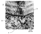
- strain can be introduced by performing ion bombarding on the surface of the coated metal layer. Since it is difficult to confirm this distortion region with an optical microscope or a scanning electron microscope (SEM), in this embodiment, the distortion region was observed from a bright field image of a transmission electron microscope (TEM).
- TEM transmission electron microscope
- 1 and 2 are sectional views of the covering member of the present embodiment. As shown in FIGS. 1 and 2, the dark color portion observed between the metal layer 1 and the B layer 2 is the strain region 3.
- TEM it is possible to observe the strain region in the covering member of this embodiment by using laser Raman spectroscopy or X-ray diffraction.
- the covering member of the present embodiment has Cr or CrM nitride, carbonitride, oxynitride, oxycarbonitride (M is a group 4 metal, group 5 metal, group 6 metal in the periodic table, 1 or 2 or more types selected from Al, Si, and B).
- the B layer may have a single layer structure depending on the purpose, or may have a multilayer structure (including an alternating layer structure) of two or more layers having different components within the above-described component range. For example, when it is desired to further improve the hardness or to further improve the durability by suppressing the progress of cracks, it is preferable to have an alternately laminated structure.
- a nitride containing 25 atomic% or more of Cr (Cr-based nitride) should be selected. Is more preferable.
- Cr-based nitride Cr-based nitride
- the thickness of the B layer is preferably set to 4 to 20 ⁇ m.
- a more preferable lower limit of the thickness of the B layer can be set to 5 ⁇ m, a more preferable thickness of the B layer can be set to 6 ⁇ m, and a more preferable upper limit of the thickness of the B layer can be set to 15 ⁇ m.
- the individual thicknesses of the b1 layer and the b2 layer are preferably 5 nm or more and 100 nm or less.
- the B layer has an alternate laminated structure in which the b1 layer and the b2 layer are alternately laminated
- the nitride of Cr or CrM that is thicker than the individual thickness of the two layers alternately laminated on the alternate laminated structure
- Carbonitride, oxynitride, oxycarbonitride (M is one or more selected from Group 4 metal, Group 5 metal, Group 6 metal, Al, Si, B in the periodic table)
- M is one or more selected from Group 4 metal, Group 5 metal, Group 6 metal, Al, Si, B in the periodic table
- the covering member of this embodiment may further have a second metal layer containing Cr, Ti, or W on the B layer.
- the second metal layer at this time may be composed of the same metal atoms as the metal layer formed between the A layer and the B layer, or may be composed of different metal atoms.
- the thickness of the second metal layer is preferably set to 0.1 to 3.0 ⁇ m.
- this 2nd metal layer can be processed in the same furnace and can improve work efficiency, it is from the same metal atom as the metal layer currently formed between A layer and B layer. It is preferable to be configured.
- a physical vapor deposition method such as an arc ion plating method, a sputtering method, or a hollow cathode method, which can improve the film adhesion, can be applied.
- the arc ion plating method is applied.
- the bias voltage during coating is preferably -150 to -40V.
- a more preferable lower limit of the bias voltage is ⁇ 120V, and a more preferable upper limit of the bias voltage is ⁇ 60V.
- the arc current is preferably 60 to 150A.
- a more preferable lower limit of the arc current is 80A, and a more preferable upper limit of the arc current is 100A.
- a polishing process for polishing the surface of the A layer may be introduced after the first coating process.
- coarse droplets and particles on the surface of the A layer can be removed, so that the occurrence of pitting caused by surface irregularities can be suppressed and the corrosion resistance of the entire coating can be improved.
- polishing cloth holding a polishing material such as diamond paste, shot blasting, ion etching treatment or the like can be applied.
- an ion etching process which can be performed in the same furnace as a film forming apparatus described later, is applied.
- preferable conditions are that Ar gas is ionized in the chamber and ion etching is performed with a bias voltage of ⁇ 600 to ⁇ 200V.
- a more preferable lower limit of the bias voltage is ⁇ 450V, and a more preferable upper limit of the bias voltage is ⁇ 300V.
- ions or radicals collide with the base material or film to scrape the surface, and the process of cleaning and smoothing is “ion etching”, and ions are collided with the metal layer to distort the surface of the metal layer.
- the process of imparting is distinguished as “ion bombardment”.
- Metal layer coating process Subsequently, a metal layer containing Cr, Ti, or W having an effect of blocking the growth of a defective structure is coated on the A layer.
- the existing physical vapor deposition method can also be applied to the coating method of the metal layer, but the film formation method used in the A layer is applied because the film formation can be performed in the same furnace to improve the working efficiency. It is preferable.
- This metal layer is preferably coated with a bias voltage set in the range of ⁇ 110V to ⁇ 60V. A more preferable lower limit of the bias voltage is ⁇ 100V.
- the Ar gas pressure can be set to 1 to 2 Pa in order to stabilize the discharge.
- a more preferred lower limit is 1.5 Pa, and a more preferred upper limit is 1.8 Pa.
- the manufacturing method of the present embodiment includes a metal layer modification step for introducing strain into the surface layer of the metal layer after the metal layer is coated.
- a metal layer modification step for introducing strain into the surface layer of the metal layer after the metal layer is coated.
- this metal layer reforming step it is possible to form a strain region in the surface layer of the metal layer that can suppress the progress of pitting corrosion from the B layer and maintain the corrosion resistance for a long period of time.
- the surface temperature of the metal ion bombardment is likely to rise more than that of the gas bombardment, and as a result, the formation of a strain region due to thermal strain when cooled is likely to be facilitated.
- a metal ion contains the metal used at the metal layer coating process.
- the strain region can be formed only by changing the bias voltage without removing the member from the furnace, so that the productivity is excellent.
- the bias voltage is preferably adjusted to -120V or less.
- the lower limit is not particularly defined, but is preferably adjusted to ⁇ 800 V or more in order to obtain a metal layer having a desired film thickness more stably.
- a more preferable bias voltage is ⁇ 250V to ⁇ 150V.
- the ion bombardment time can be set to 5 to 30 minutes when metal ions are applied, and 5 to 20 minutes when Ar ions are applied. Note that when Ar ion bombardment is performed, the bias voltage may be adjusted as appropriate so that the metal layer is not cut and distortion occurs.
- Cr or CrM nitride, carbonitride, oxynitride, oxycarbonitride is formed on the metal layer subjected to the metal layer modification step.
- the coating means and coating conditions can be the same as in the first coating step, but depending on the desired application, a single layer film or two or more layers (including alternating layers) with different components can be used. It can select and coat
- the manufacturing method of this embodiment can also implement the 2nd metal layer coating process which coat
- the coating conditions for the second metal layer may be set to the same conditions as those for the metal layer formed on the A layer described above.
- a base material (YPT42 (manufactured by Hitachi Metals)) was prepared.
- the coating apparatus an arc ion plating apparatus was used, and Cr and TiW were prepared as targets for A layer film formation and metal ion bombardment, and AlCrSi, CrSi, and AlCr were prepared as targets for B layer film formation.
- the surface of the base material was polished to an average roughness Ra of 0.05 ⁇ m and Rz of 0.1 ⁇ m, degreased and washed, and fixed to the base material holder. And the base material was heated to about 500 degreeC with the heater for heating installed in the chamber, and was hold
- Ar gas was introduced, a bias voltage of ⁇ 200 V was applied to the substrate, and a 20 minute plasma cleaning process (Ar ion etching) was performed. Subsequently, the bias voltage applied to the substrate was changed to ⁇ 800 V, and Cr ion bombardment was performed for about 20 minutes.
- Example 1 ⁇ Sample No. 1> Under conditions of a substrate temperature of 500 ° C. and a reaction gas pressure of 4.0 Pa, the bias voltage was set to ⁇ 60 V, and CrN as the A layer was coated by about 6 ⁇ m (first coating process), and then Ar etching was performed at a bias voltage of ⁇ 300 V. Then, the bias voltage was set to ⁇ 100 V and 1 ⁇ m of Cr as the metal layer was coated (metal layer coating step).
- Example No. 4 Layer A is sample No. The same conditions as in No. 1 were applied. Once the layer A is coated, the sample is once taken out of the furnace, and the sample surface is polished for about 5 minutes using an aero lapping device AERO LAP YT-300 (Aero Wrap is a registered trademark of Yamashita Towers Co., Ltd.) manufactured by Yamashita Towers.
- the arithmetic average roughness Ra of the surface was adjusted to 0.01 ⁇ m, and the maximum height Rz was adjusted to 2.00 ⁇ m or less. Subsequently, the sample was returned to the furnace. After coating the metal layer under the same conditions as 1, the surface of the metal layer was subjected to ion bombardment with Ar gas under the condition of a bias voltage of ⁇ 200 V to form a strained region. Subsequently, an AlCrSiN / CrN alternating laminated film (thickness of each layer: 20 to 30 nm) serving as a B layer under a bias voltage of ⁇ 80 V was coated with about 3 ⁇ m, and CrN was coated as an upper layer with 3 ⁇ m. ⁇ Sample No.
- the bias voltage was set to ⁇ 80 V and AlCrN as the A layer was coated by about 6 ⁇ m (first coating process), and then Ar etching was performed at a bias voltage of ⁇ 300 V. Then, the bias voltage was set to ⁇ 100 V and 1 ⁇ m of Cr as the metal layer was coated (metal layer coating step). Thereafter, the bias voltage was changed to ⁇ 120 V, and metal ion bombardment with Cr ions was performed on the surface of the metal layer for about 10 minutes to form a strain region (metal layer modification step).
- a CrSiBN / AlCrN alternating laminated film (thickness of each layer: 20 to 30 nm), which becomes a B layer under a bias voltage of ⁇ 100 V, is coated with about 6 ⁇ m (second coating step), and CrSiBN is 3 ⁇ m as an upper layer of the B layer. Covered.
- Sample No. 2 was set to the same conditions. ⁇ Sample No. 11> Layer A is sample No. The same conditions as in No. 1 were applied. Thereafter, the bias voltage at the time of the metal layer coating step and the metal layer reforming step was measured as Sample No. A sample was prepared by setting it higher than the condition 1 and adjusting so as not to form a strain region.
- Sample No. 2 was set to the same conditions. ⁇ Sample No. 12> Layer A is sample No. The same conditions as in No. 1 were applied. Thereafter, the bias voltage at the time of the metal layer coating step was also set as Sample No. 1 and the bias voltage at the time of the metal layer reforming step is the same as the sample No. A sample was prepared by setting it higher than the condition 1 and adjusting so as not to form a strain region. Others are Sample No. 2 was set to the same conditions. ⁇ Sample No. 13> The A layer is designated as Sample No. The same conditions as in No. 1 were applied. Thereafter, Ar etching was performed at a bias voltage of ⁇ 300V. Thereafter, without performing the metal layer coating step and the metal layer modification step, the sample No. The layer B was coated under the same conditions as 2, and the upper layer was coated with 3 ⁇ m of CrN.
- the corrosion resistance evaluation test was performed on the prepared sample.
- a test was conducted in which a sample was immersed in a 10% sulfuric acid aqueous solution for 10 hours while simulating a corrosive gas such as a halogen gas and a sulfide gas generated during actual injection molding.
- the temperature of the aqueous solution was 50 ° C., and in accordance with JIS-G-0591-2007, portions other than the coated surface of the test piece were masked, and pitting corrosion appearing on the surface after immersion was observed.
- the state of pitting corrosion on the test surface ( ⁇ 18 mm) was evaluated by a stereoscopic microscope photograph (magnification: ⁇ 10) using a Nikon stereo microscope.
- Corrosion resistance is evaluated in the stereomicrographs when there is a pitting corrosion having a size of 0.2 mm or more and less than 0.8 mm, when the pitting corrosion is less than 0.2 mm, The case where no spot-like corrosion occurred was marked as ⁇ . The number of pitting corrosion of each size was measured. The evaluation results are shown in Table 1.
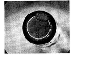
- FIG. 1 shows a photograph of a sample surface after 30 hours of corrosion resistance test No. 1. Sample No. In No. 2, slight corrosion was observed after 40 hours. No corrosion was observed even after 1 hour, and it was confirmed that No. 1 showed very good corrosion resistance. Although not shown in the figure, the sample No. 6 and sample no. For sample No. 7, sample no. Similar to 1, it was confirmed that no corrosion was observed even after 50 hours.
- FIG. 1 was cut in the film thickness direction, and the cross section was confirmed with a TEM manufactured by JEOL (measurement condition: acceleration voltage 200 kV).
- FIG. 1 is a TEM photograph of a sample cross section showing the vicinity of the boundary between the metal layer and the B layer
- FIG. 2 is an enlarged TEM photograph of the region A in FIG. 1 in order to confirm the strain region.
- a dark strain region is formed between the Cr layer 1 as the metal layer and the AlCrSiN / CrN multilayer film 2 as the B layer on the upper surface side (B layer side) of the metal layer 1. It was.
- Example 2 Subsequently, the evaluation of melt resistance was performed.
- a DAC manufactured by Hitachi Metals, hardness: about 45 HRC
- Cr was prepared as a target for film formation and metal ion bombardment
- AlCrSi was prepared as a target for hard components.
- the surface of the base material was polished to an average roughness Ra of 0.05 ⁇ m and Rz of 0.1 ⁇ m, degreased and washed, and fixed to the base material holder. And the base material was heated to about 500 degreeC with the heater for heating installed in the chamber, and was hold
- Example No. 15 An AlCrSiN film of about 3 ⁇ m was coated under conditions of a substrate temperature of 500 ° C. and a reaction gas pressure of 4.0 Pa and a bias voltage of ⁇ 80 V. 15 was produced.
- the prepared sample No. 8, no. 14, no. 15 was subjected to a erosion resistance evaluation test.
- the present invention example and the comparative example were immersed in a molten aluminum at 700 ° C. for 30 hours, and the presence or absence of melting damage was confirmed by an optical microscope. In addition, the mass loss before and after the test was measured, and the melting rate (%) was confirmed.
- the results of the erosion test of the inventive example and the comparative example are shown in FIGS. As shown in FIG. 5 and FIG. No melting failure was observed even after 30 hours, and the melting loss rate was 0.0%, showing a very good result. In contrast, Sample No. As shown in FIG. 7 and FIG. The melting rate is 1.3%. It was confirmed that the meltability was lower than 8. Furthermore, sample No. of the comparative example.
Landscapes
- Chemical & Material Sciences (AREA)
- Engineering & Computer Science (AREA)
- Mechanical Engineering (AREA)
- Chemical Kinetics & Catalysis (AREA)
- Materials Engineering (AREA)
- Metallurgy (AREA)
- Organic Chemistry (AREA)
- Manufacturing & Machinery (AREA)
- Physical Vapour Deposition (AREA)
- Moulds For Moulding Plastics Or The Like (AREA)
Abstract
Description
即ち本発明の一態様は、基材の表面に硬質皮膜を有する、被覆部材であって、
前記硬質皮膜は、CrまたはCrMの窒化物、炭窒化物、酸窒化物、酸炭窒化物(Mは周期表の4族金属、5族金属、6族金属、Al、Si、Bから選択される1種または2種以上)から選択されるA層と、
A層よりも外表面側に形成され、Cr、Ti、またはWを含む金属層と、
前記金属層よりも外表面側に形成され、CrまたはCrMの窒化物、炭窒化物、酸窒化物、酸炭窒化物(Mは周期表の4族金属、5族金属、6族金属、Al、Si、Bから選択される1種または2種以上)から選択されるB層と、を備え、
前記金属層の外表面側は、歪みが導入されていることを特徴とする、被覆部材である。
好ましくは、前記B層よりも外表面側に、Cr、Ti、またはWを含む第二金属層を備える。
好ましくは、前記A層およびB層の少なくとも一方の厚さが4~20μmである。
好ましくは、前記A層およびB層の少なくとも一方の厚さが6μm以上である。
基材にCrまたはCrMの窒化物、炭窒化物、酸窒化物、酸炭窒化物(Mは周期表の4族金属、5族金属、6族金属、Al、Si、Bから選択される1種または2種以上)から選択されるA層を被覆する第一被覆工程と、
A層を被覆した後に、Cr、Ti、またはWを含む金属層を被覆する金属層被覆工程と、
金属層を被覆した後に、金属層の表層に歪みを導入する、金属層改質工程と、
金属層改質工程後に、CrまたはCrMの窒化物、炭窒化物、酸窒化物、酸炭窒化物(Mは周期表の4族金属、5族金属、6族金属、Al、Si、Bから選択される1種または2種以上)から選択される層を被覆する第二被覆工程と、を備えることを特徴とする、被覆部材の製造方法である。
好ましくは、前記金属層改質工程は、CrイオンまたはTiイオンを含む金属イオンボンバードである。
好ましくは、前記第一被覆工程と金属層被覆工程との間に、A層の表面を研磨する研磨工程を行う。
好ましくは、前記第二被覆工程の後に、Cr、TiまたはWを含む第二金属層を被覆する第二金属層被覆工程を備える。
(第一被覆工程)
本実施形態の製造方法では、まず基材にCrまたはCrMの窒化物、炭窒化物、酸窒化物、酸炭窒化物(Mは周期表の4族金属、5族金属、6族金属、Al、Si、Bから選択される1種または2種以上)から選択されるA層を被覆する。耐食性に優れるCr系の窒化物皮膜を選択することが好ましい。A層の被覆手段は、皮膜密着性を高めることができるアークイオンプレーティング法やスパッタリング法、ホローカソード法などの物理蒸着法を適用することができる。本実施形態では、アークイオンプレーティング法を適用している。被覆時のバイアス電圧は-150~-40Vで実施することが好ましい。より好ましいバイアス電圧の下限は-120Vであり、より好ましいバイアス電圧の上限は-60Vである。またアーク電流は60~150Aが好ましい。より好ましいアーク電流の下限は80Aであり、より好ましいアーク電流の上限は100Aである。
本実施形態では第一被覆工程後、A層の表面を研摩する研摩工程を導入してもよい。これによりA層の表面における粗大なドロップレットやパーティクルを除去することができるため、表面凹凸に起因する孔食の発生を抑制し、皮膜全体の耐食性を向上させることが可能である。この研摩手段には、ダイヤモンドペースト等の研摩材を保持した研摩布、ショットブラスト、イオンエッチング処理等を適用することができる。好ましくは、後述する成膜装置と同一炉内で処理可能である、イオンエッチング処理を適用する。研摩工程にイオンエッチング処理を適用した場合、好ましい条件は、Arガスをチャンバー内でイオン化させ、-600~-200Vのバイアス電圧をでイオンエッチングを行う。より好ましいバイアス電圧の下限は-450Vであり、より好ましいバイアス電圧の上限は-300Vである。なお本実施形態では、イオン(またはラジカル)を基材や皮膜に衝突させて表面を削り、洗浄や平滑化を行う工程を「イオンエッチング」、イオンを金属層に衝突させて金属層表面に歪みを付与する工程を「イオンボンバード」として区別する。
続いて、A層上に、欠陥組織の成長を遮断する効果を有するCr、Ti、またはWを含む金属層を被覆する。この金属層の被覆方法についても、既存の物理蒸着法を適用することができるが、同一炉内で成膜して作業効率を高めることができるため、A層で用いた成膜方法を適用することが好ましい。この金属層は、バイアス電圧を-110V~-60Vの範囲に設定して被覆することが好ましい。より好ましいバイアス電圧の下限は、-100Vである。上述したバイアス電圧の範囲内に調整することで、金属層の密着性が向上すると共に金属層の組織が緻密化するといった利点がある。この第一被覆工程においては、Arを微量流しながら成膜することが好ましい。このとき、放電を安定させるためArガス圧力は1~2Paに設定することができる。より好ましい下限は1.5Paであり、より好ましい上限は1.8Paである。
本実施形態の製造方法では、金属層を被覆後に、金属層の表層に歪みを導入する金属層改質工程を備える。この金属層改質工程により、B層からの孔食の進行を抑制し、長期間にわたって耐食性を維持することを可能とする歪み領域を、金属層の表層に形成することができる。この歪み領域を形成させるためには、金属イオンやArイオンによるボンバードを実施することが好ましい。より好ましくは金属イオンボンバードを実施する。これはArイオンに比べて金属イオンの方が質量が大きいため,表面に衝突した際に効率的に歪みを付与できる傾向にあるからである。また、金属イオンボンバード中は表面温度がガスボンバードよりも上昇しやすく、結果的に冷却された際の熱ひずみによる歪み領域形成が容易となる傾向にある。ここで本実施形態において金属イオンボンバードを適用する場合、金属イオンは金属層被覆工程で使用した金属を含むことが好ましい。これにより、炉から部材を取りださず、バイアス電圧を変更するだけで歪み領域を形成させることができるため、生産性に優れる。この金属イオンボンバードを行う際、バイアス電圧は-120V以下に調整することが好ましい。下限は特に規定しないが、より安定して所望の膜厚の金属層を得るために、-800V以上に調整することが好ましい。より好ましいバイアス電圧は、-250V~-150Vである。このバイアス電圧に調整することで、上述した歪み領域を安定して形成させることが可能である。またイオンボンバード時間は、金属イオンを適用する場合は5~30min、Arイオンを適用する場合は5~20minと設定することができる。なおArイオンボンバードを行う際、バイアス電圧は金属層が削れず、歪みが入る値に適宜調整すればよい。
本実施形態の製造方法は、金属層改質工程を施した金属層の上に、CrまたはCrMの窒化物、炭窒化物、酸窒化物、酸炭窒化物(Mは周期表の4族金属、5族金属、6族金属、Al、Si、Bから選択される1種または2種以上)から選択されるB層を被覆する第二被覆工程を備える。被覆手段や被覆条件は第一被覆工程と同様の条件を適用することが可能であるが、所望する用途によって単層膜、成分の異なる二層以上の複層膜(交互積層膜も含む)を適宜選択して被覆することができる。例えばCrNとAlCrSiNとの交互積層膜を被覆する場合は、CrターゲットとAlCrSiターゲットを同時放電させるといった製造方法で作製することができる。
(実施例1)
<試料No.1>
基材温度500℃、反応ガス圧力4.0Paの条件で、バイアス電圧を-60Vに設定してA層であるCrNを約6μm被覆(第一被覆工程)後、バイアス電圧-300VでArエッチングを行い、バイアス電圧を-100Vに設定して金属層であるCrを1μm被覆した(金属層被覆工程)。その後バイアス電圧を-120Vに変更し、金属層の表面にCrイオンによる金属イオンボンバードを約10分間行い、歪み領域を形成した(金属層改質工程)。続いてバイアス電圧-80Vの条件でB層となるAlCrSiN/CrN交互積層膜(各層の厚さ:20~30nm)を約6μm被覆し(第二被覆工程)、B層の上部層としてCrNを3μm被覆した。
<試料No.2>
第一被覆工程から金属層改質工程まで試料No.1と同じ条件で行った。続いてバイアス電圧を-80Vの条件でB層となるAlCrSiN/CrN交互積層膜(各層の厚さ:20~30nm)を約3μm被覆し、上部層としてCrNを3μm被覆した。
<試料No.3>
第一被覆工程から金属層被覆工程まで試料No.1と同じ条件で行った。その後バイアス電圧を-200Vに変更し、金属層の表面にバイアス電圧-200Vの条件でArガスによるイオンボンバードを行い、歪み領域を形成した。続いて、バイアス電圧-80Vの条件でB層となるAlCrSiN/CrN交互積層膜(各層の厚さ:20~30nm)を約3μm被覆し、上部層としてCrNを3μm被覆した。
<試料No.4>
A層は試料No.1と同じ条件で被覆した。A層被覆後に一旦炉から試料を取り出し、ヤマシタワークス社製エアロラップ装置AERO LAP YT-300(エアロラップは、株式会社ヤマシタワークスの登録商標)を用いて試料表面を5分程度研磨し、A層表面の算術平均粗さRa=0.01μm,最大高さRz=2.00μm以下となるように調整した。続いて試料を炉に戻し、試料No.1と同じ条件で金属層を被覆した後、金属層の表面にバイアス電圧-200Vの条件でArガスによるイオンボンバードを行い、歪み領域を形成した。続いてバイアス電圧-80Vの条件でB層となるAlCrSiN/CrN交互積層膜(各層の厚さ:20~30nm)を約3μm被覆し、上部層としてCrNを3μm被覆した。
<試料No.5>
A層であるCrNを約4μm被覆した後、バイアス電圧-300VでArエッチングを行った。その後の金属層被覆工程以降は、試料No.2と同じ条件に設定した。
<試料No.6>
第一工程は試料No.1と同じ条件で行った。その後、バイアス電圧-300VでArエッチングを行い、バイアス電圧を-100Vに設定して金属層であるTiWを1μm被覆した(金属層被覆工程)。その後バイアス電圧を-120Vに変更し、金属層の表面にTiイオンとWイオンによる金属イオンボンバードを約10分間行い、歪み領域を形成した(金属層改質工程)。続いてバイアス電圧-80Vの条件でB層となるAlCrSiN/CrN交互積層膜(各層の厚さ:20~30nm)を約6μm被覆し(第二被覆工程)、B層の上部層としてCrNを3μm被覆した。その後の金属層被覆工程以降は、試料No.2と同じ条件に設定した。
<試料No.7>
基材温度500℃、反応ガス圧力4.0Paの条件で、バイアス電圧を-80Vに設定してA層であるAlCrNを約6μm被覆(第一被覆工程)後、バイアス電圧-300VでArエッチングを行い、バイアス電圧を-100Vに設定して金属層であるCrを1μm被覆した(金属層被覆工程)。その後バイアス電圧を-120Vに変更し、金属層の表面にCrイオンによる金属イオンボンバードを約10分間行い、歪み領域を形成した(金属層改質工程)。続いてバイアス電圧-100Vの条件でB層となるCrSiBN/AlCrN交互積層膜(各層の厚さ:20~30nm)を約6μm被覆し(第二被覆工程)、B層の上部層としてCrSiBNを3μm被覆した。その後の金属層被覆工程以降は、試料No.2と同じ条件に設定した。
<試料No.11>
A層は試料No.1と同じ条件で被覆した。その後、金属層被覆工程時および金属層改質工程時のバイアス電圧を、試料No.1の条件よりも高く設定し、歪み領域が形成されないように調整して試料を作製した。その他は、試料No.2と同じ条件に設定した。
<試料No.12>
A層は試料No.1と同じ条件で被覆した。その後、金属層被覆工程時のバイアス電圧も試料No.1と同様の値とし、金属層改質工程時のバイアス電圧を、試料No.1の条件よりも高く設定し、歪み領域が形成されないように調整して試料を作製した。その他は、試料No.2と同じ条件に設定した。
<試料No.13>
A層を試料No.1と同じ条件で被覆した。その後、バイアス電圧-300VでArエッチングを行った。その後、金属層被覆工程および金属層改質工程を行わず、A層の上に試料No.2と同じ条件でB層を被覆し、上部層としてCrNを3μm被覆した。

続いて、良好な結果を示した試料No.1を膜厚方向に切断し、断面をJEOL製TEM(測定条件:加速電圧 200kV)で確認した。その結果を図1および図2に示す。図1は金属層とB層との境界付近を表した試料断面のTEM写真であり、図2は歪み領域を確認するために、図1のA領域を拡大したTEM写真である。図1および図2に示すように、本発明例である試料No.1の金属層上面側(B層側)には、金属層であるCr層1とB層であるAlCrSiN/CrN多層膜2との間に、暗色の歪み領域が形成されていることが確認できた。
続いて、耐溶損性の評価を行った。基材にはDAC(日立金属株式会社製、硬さ:45HRC程度)を準備した。被覆装置はアークイオンプレーティング装置を用い、成膜兼金属イオンボンバード用ターゲットとしてCrを、硬質成分用ターゲットとしてAlCrSiを準備した。基材にA層を被覆する前に、基材の表面を平均粗さRa0.05μm、Rz0.1μmに研磨し、脱脂洗浄して、基材ホルダーに固定した。そして、チャンバーに設置された加熱用ヒーターにより、基材を500℃付近に加熱し、50分間保持した。次に、Arガスを導入し、基材には-200Vのバイアス電圧を印加して、20分間のプラズマクリーニング処理(Arイオンエッチング)を行った。続いて、基材に印加するバイアス電圧を-800Vに変更して、約20分間Crボンバードを行った。
<試料No.8>
基材温度500℃、反応ガス圧力4.0Paの条件で、A層であるCrNを約6μm被覆(第一被覆工程)後、バイアス電圧-300VでArエッチングを行い、バイアス電圧を-100Vに設定して金属層であるCrを1μm被覆した(金属層被覆工程)。その後バイアス電圧を-120Vに変更し、金属層の表面にCrイオンによる金属イオンボンバードを約10分間行い、歪み領域を形成した(金属層改質工程)。続いてバイアス電圧-80Vの条件でB層となるAlCrSiN/CrN交互積層膜(各層の厚さ:20~30nm)を約6μm被覆し(第二被覆工程)、B層の上部層としてCrNを3μm被覆し、本発明である試料No.8を作製した。
<試料No.14>
基材温度500℃、反応ガス圧力4.0Paの条件で、バイアス電圧を-50VでCrNを約3μm被覆後、バイアス電圧-80Vの条件でAlCrSiN/CrN交互積層膜(各層の厚さ:20~30nm)を約4μm被覆し、さらにその上部層としてCrNを3μm被覆し、比較例である試料No.14を作製した。
<試料No.15>
基材温度500℃、反応ガス圧力4.0Paの条件で、バイアス電圧を-80Vの条件でAlCrSiN膜を約3μm被覆し、比較例である試料No.15を作製した。
図5および図6に示すように、本発明例の試料No.8は30時間経過したあとでも溶損が確認されず、溶損率は0.0%と非常に良好な結果を示した。対して比較例の試料No.14は図7および図8に示すように試料に溶損が発生した。その溶損率は1.3%であり、試料No.8よりも低い溶損性を示すことが確認できた。さらに比較例の試料No.15に関しては、試験開始から6時間の時点で、図9および図10に示すような大きい溶損が発生したため、試験を中止した。このときの溶損率は23%であった。No.15の溶損進行が速い理由としては、膜厚が薄く、被膜の構造も単層であったため、貫通欠陥が発生しやすかったことが原因と考えられる。
2 B層
3 歪み領域
4 孔食
Claims (8)
- 基材の表面に硬質皮膜を有する被覆部材であって、
前記硬質皮膜は、CrまたはCrMの窒化物、炭窒化物、酸窒化物、酸炭窒化物(Mは周期表の4族金属、5族金属、6族金属、Al、Si、Bから選択される1種または2種以上)から選択されるA層と、
前記A層よりも外表面側に形成され、Cr、Ti、またはWを含む金属層と、
前記金属層よりも外表面側に形成され、CrまたはCrMの窒化物、炭窒化物、酸窒化物、酸炭窒化物(Mは周期表の4族金属、5族金属、6族金属、Al、Si、Bから選択される1種または2種以上)から選択されるB層と、を備え、
前記金属層の外表面側は、歪みが導入されていることを特徴とする、被覆部材。 - 前記B層よりも外表面側に、Cr、Ti、またはWを含む第二金属層を備えることを特徴とする、請求項1に記載の被覆部材。
- 前記A層およびB層の少なくとも一方の厚さが4~20μmであることを特徴とする、請求項1または2に記載の被覆部材。
- 前記A層およびB層の少なくとも一方の厚さが6μm以上であることを特徴とする、請求項3に記載の被覆部材。
- 基材の表面に硬質皮膜を有する被覆部材の製造方法であって、
基材にCrまたはCrMの窒化物、炭窒化物、酸窒化物、酸炭窒化物(Mは周期表の4族金属、5族金属、6族金属、Al、Si、Bから選択される1種または2種以上)から選択されるA層を被覆する第一被覆工程と、
前記A層を被覆した後に、Cr、Ti、またはWを含む金属層を被覆する金属層被覆工程と、
前記金属層を被覆した後に、前記金属層の表層に歪みを導入する、金属層改質工程と、
前記金属層改質工程後に、CrまたはCrMの窒化物、炭窒化物、酸窒化物、酸炭窒化物(Mは周期表の4族金属、5族金属、6族金属、Al、Si、Bから選択される1種または2種以上)から選択される層を被覆する第二被覆工程と、を備えることを特徴とする、被覆部材の製造方法。 - 前記金属層改質工程は、CrイオンまたはTiイオンを含む金属イオンボンバードであることを特徴とする、請求項5に記載の被覆部材の製造方法。
- 前記第一被覆工程と金属層被覆工程との間に、A層の表面を研磨する研磨工程を行うことを特徴とする、請求項5または6に記載の被覆部材の製造方法。
- 前記第二被覆工程の後に、Cr、TiまたはWを含む第二金属層を被覆する第二金属層被覆工程を備えることを特徴とする、請求項5乃至7のいずれかに記載の被覆部材の製造方法。
Priority Applications (5)
| Application Number | Priority Date | Filing Date | Title |
|---|---|---|---|
| US16/971,688 US11976350B2 (en) | 2018-02-27 | 2019-02-15 | Covering member and method for manufacturing the same |
| KR1020207023189A KR102317383B1 (ko) | 2018-02-27 | 2019-02-15 | 피복부재 및 그 제조 방법 |
| EP19761278.1A EP3760757A4 (en) | 2018-02-27 | 2019-02-15 | COATING ELEMENT AND ITS MANUFACTURING PROCESS |
| CN201980014445.6A CN111771011B (zh) | 2018-02-27 | 2019-02-15 | 被覆构件及其制造方法 |
| JP2019525932A JP6593667B1 (ja) | 2018-02-27 | 2019-02-15 | 被覆部材およびその製造方法 |
Applications Claiming Priority (2)
| Application Number | Priority Date | Filing Date | Title |
|---|---|---|---|
| JP2018-032834 | 2018-02-27 | ||
| JP2018032834 | 2018-02-27 |
Publications (1)
| Publication Number | Publication Date |
|---|---|
| WO2019167674A1 true WO2019167674A1 (ja) | 2019-09-06 |
Family
ID=67806205
Family Applications (1)
| Application Number | Title | Priority Date | Filing Date |
|---|---|---|---|
| PCT/JP2019/005573 Ceased WO2019167674A1 (ja) | 2018-02-27 | 2019-02-15 | 被覆部材およびその製造方法 |
Country Status (6)
| Country | Link |
|---|---|
| US (1) | US11976350B2 (ja) |
| EP (1) | EP3760757A4 (ja) |
| JP (1) | JP6593667B1 (ja) |
| KR (1) | KR102317383B1 (ja) |
| CN (1) | CN111771011B (ja) |
| WO (1) | WO2019167674A1 (ja) |
Citations (5)
| Publication number | Priority date | Publication date | Assignee | Title |
|---|---|---|---|---|
| JP2000256878A (ja) * | 1999-03-09 | 2000-09-19 | Sumitomo Metal Mining Co Ltd | 高耐食性膜付き部材及びその製造方法 |
| JP2009078351A (ja) | 2007-09-26 | 2009-04-16 | Sandvik Intellectual Property Ab | 被膜付き切削工具の製造方法 |
| WO2009119269A1 (ja) * | 2008-03-28 | 2009-10-01 | 日立金属株式会社 | 皮膜密着性に優れた表面被覆部品の製造方法 |
| WO2011125657A1 (ja) | 2010-03-31 | 2011-10-13 | 日立ツール株式会社 | 耐食性に優れた被覆物品の製造方法および被覆物品 |
| WO2016027832A1 (ja) | 2014-08-20 | 2016-02-25 | 日立金属株式会社 | ダイカスト用被覆金型の製造方法 |
Family Cites Families (12)
| Publication number | Priority date | Publication date | Assignee | Title |
|---|---|---|---|---|
| CA2092932C (en) * | 1992-04-17 | 1996-12-31 | Katsuya Uchino | Coated cemented carbide member and method of manufacturing the same |
| CA2327031C (en) * | 1999-11-29 | 2007-07-03 | Vladimir Gorokhovsky | Composite vapour deposited coatings and process therefor |
| EP2865784A1 (en) * | 2002-08-08 | 2015-04-29 | Kabushiki Kaisha Kobe Seiko Sho (Kobe Steel, Ltd.) | Process for producing alumina coating composed mainly of alpha-type crystal structure |
| CN100479955C (zh) * | 2003-12-05 | 2009-04-22 | 住友电工硬质合金株式会社 | 表面被覆切削工具 |
| JP4704335B2 (ja) * | 2004-03-18 | 2011-06-15 | 住友電工ハードメタル株式会社 | 表面被覆切削工具 |
| JP2009061465A (ja) * | 2007-09-05 | 2009-03-26 | Daido Steel Co Ltd | 冷間鍛造用金型及びその製造方法 |
| KR20120129445A (ko) * | 2011-05-20 | 2012-11-28 | 경성대학교 산학협력단 | 내산화성 내마모성의 복합 다층 코팅층 제조. |
| US9492872B2 (en) * | 2011-08-01 | 2016-11-15 | Hitachi Tool Engineering, Ltd. | Surface-modified, WC-based cemented carbide member, hard-coated, WC-based cemented carbide member, and their production methods |
| ES2677711T3 (es) * | 2011-09-28 | 2018-08-06 | Hitachi Metals, Ltd. | Elemento recubierto con excelentes propiedades de deslizamiento |
| KR20130060544A (ko) * | 2011-11-30 | 2013-06-10 | 현대자동차주식회사 | 나노멀티레이어 코팅층 형성방법 및 형성장치 |
| EP2883637B1 (en) * | 2012-08-10 | 2018-02-28 | Tungaloy Corporation | Coated tool |
| EP3722031A1 (en) * | 2014-03-18 | 2020-10-14 | Hitachi Metals, Ltd. | Coated cutting tool and method for producing the same |
-
2019
- 2019-02-15 CN CN201980014445.6A patent/CN111771011B/zh active Active
- 2019-02-15 US US16/971,688 patent/US11976350B2/en active Active
- 2019-02-15 WO PCT/JP2019/005573 patent/WO2019167674A1/ja not_active Ceased
- 2019-02-15 KR KR1020207023189A patent/KR102317383B1/ko active Active
- 2019-02-15 EP EP19761278.1A patent/EP3760757A4/en active Pending
- 2019-02-15 JP JP2019525932A patent/JP6593667B1/ja active Active
Patent Citations (5)
| Publication number | Priority date | Publication date | Assignee | Title |
|---|---|---|---|---|
| JP2000256878A (ja) * | 1999-03-09 | 2000-09-19 | Sumitomo Metal Mining Co Ltd | 高耐食性膜付き部材及びその製造方法 |
| JP2009078351A (ja) | 2007-09-26 | 2009-04-16 | Sandvik Intellectual Property Ab | 被膜付き切削工具の製造方法 |
| WO2009119269A1 (ja) * | 2008-03-28 | 2009-10-01 | 日立金属株式会社 | 皮膜密着性に優れた表面被覆部品の製造方法 |
| WO2011125657A1 (ja) | 2010-03-31 | 2011-10-13 | 日立ツール株式会社 | 耐食性に優れた被覆物品の製造方法および被覆物品 |
| WO2016027832A1 (ja) | 2014-08-20 | 2016-02-25 | 日立金属株式会社 | ダイカスト用被覆金型の製造方法 |
Non-Patent Citations (1)
| Title |
|---|
| See also references of EP3760757A4 |
Also Published As
| Publication number | Publication date |
|---|---|
| EP3760757A1 (en) | 2021-01-06 |
| KR102317383B1 (ko) | 2021-10-26 |
| CN111771011B (zh) | 2022-07-05 |
| JPWO2019167674A1 (ja) | 2020-04-16 |
| US20200407837A1 (en) | 2020-12-31 |
| KR20200106537A (ko) | 2020-09-14 |
| EP3760757A4 (en) | 2021-12-01 |
| US11976350B2 (en) | 2024-05-07 |
| CN111771011A (zh) | 2020-10-13 |
| JP6593667B1 (ja) | 2019-10-23 |
Similar Documents
| Publication | Publication Date | Title |
|---|---|---|
| US20140044944A1 (en) | Coating material for aluminum die casting mold and method of manufacturing the coating material | |
| JP6525310B2 (ja) | 被覆工具 | |
| KR102345375B1 (ko) | 피복 절삭 공구 | |
| JP6658983B2 (ja) | 被覆切削工具 | |
| JP4311803B2 (ja) | 表面被覆成形型およびその製造方法 | |
| KR20090032016A (ko) | 코팅된 절삭 공구를 제조하는 방법 | |
| JP5435326B2 (ja) | ダイカスト用被覆金型およびその製造方法 | |
| WO2015141743A1 (ja) | 被覆切削工具及びその製造方法 | |
| JP5498572B2 (ja) | 耐食性に優れた被覆物品の製造方法および被覆物品 | |
| JP5765627B2 (ja) | 耐久性に優れる被覆工具およびその製造方法 | |
| JP2013096004A (ja) | 耐剥離性に優れる被覆工具およびその製造方法 | |
| JP6274317B2 (ja) | ダイカスト用被覆金型の製造方法 | |
| JP2021025132A (ja) | 被覆部材およびその製造方法 | |
| JP6593667B1 (ja) | 被覆部材およびその製造方法 | |
| JP2012152878A (ja) | 耐摩耗性と摺動特性に優れる被覆工具およびその製造方法 | |
| JP6805320B1 (ja) | 多層皮膜、その製造方法、及び多層皮膜が被覆された機械部材 | |
| JPWO2019035219A1 (ja) | 被覆切削工具 | |
| JP2006002227A (ja) | 硬質皮膜の製造方法 | |
| JP5892414B2 (ja) | 耐食性に優れた被覆物品の製造方法および被覆物品 | |
| JP7760424B2 (ja) | 被覆部材 | |
| JP4154024B2 (ja) | 耐溶損性に優れるAl又はAl合金溶湯用の鋳造用部材 | |
| JP2007217771A (ja) | 硬質皮膜被覆部材及びその製造方法 | |
| JP2013227640A (ja) | 耐食性に優れた被覆物品およびその製造方法 |
Legal Events
| Date | Code | Title | Description |
|---|---|---|---|
| ENP | Entry into the national phase |
Ref document number: 2019525932 Country of ref document: JP Kind code of ref document: A |
|
| 121 | Ep: the epo has been informed by wipo that ep was designated in this application |
Ref document number: 19761278 Country of ref document: EP Kind code of ref document: A1 |
|
| ENP | Entry into the national phase |
Ref document number: 20207023189 Country of ref document: KR Kind code of ref document: A |
|
| NENP | Non-entry into the national phase |
Ref country code: DE |
|
| ENP | Entry into the national phase |
Ref document number: 2019761278 Country of ref document: EP Effective date: 20200928 |