WO2019171901A1 - 炭化珪素単結晶の製造方法 - Google Patents
炭化珪素単結晶の製造方法 Download PDFInfo
- Publication number
- WO2019171901A1 WO2019171901A1 PCT/JP2019/005388 JP2019005388W WO2019171901A1 WO 2019171901 A1 WO2019171901 A1 WO 2019171901A1 JP 2019005388 W JP2019005388 W JP 2019005388W WO 2019171901 A1 WO2019171901 A1 WO 2019171901A1
- Authority
- WO
- WIPO (PCT)
- Prior art keywords
- silicon carbide
- single crystal
- raw material
- carbon
- carbide single
- Prior art date
- Legal status (The legal status is an assumption and is not a legal conclusion. Google has not performed a legal analysis and makes no representation as to the accuracy of the status listed.)
- Ceased
Links
Images


Classifications
-
- C—CHEMISTRY; METALLURGY
- C30—CRYSTAL GROWTH
- C30B—SINGLE-CRYSTAL GROWTH; UNIDIRECTIONAL SOLIDIFICATION OF EUTECTIC MATERIAL OR UNIDIRECTIONAL DEMIXING OF EUTECTOID MATERIAL; REFINING BY ZONE-MELTING OF MATERIAL; PRODUCTION OF A HOMOGENEOUS POLYCRYSTALLINE MATERIAL WITH DEFINED STRUCTURE; SINGLE CRYSTALS OR HOMOGENEOUS POLYCRYSTALLINE MATERIAL WITH DEFINED STRUCTURE; AFTER-TREATMENT OF SINGLE CRYSTALS OR A HOMOGENEOUS POLYCRYSTALLINE MATERIAL WITH DEFINED STRUCTURE; APPARATUS THEREFOR
- C30B23/00—Single-crystal growth by condensing evaporated or sublimed materials
- C30B23/02—Epitaxial-layer growth
- C30B23/06—Heating of the deposition chamber, the substrate or the materials to be evaporated
- C30B23/066—Heating of the material to be evaporated
-
- C—CHEMISTRY; METALLURGY
- C30—CRYSTAL GROWTH
- C30B—SINGLE-CRYSTAL GROWTH; UNIDIRECTIONAL SOLIDIFICATION OF EUTECTIC MATERIAL OR UNIDIRECTIONAL DEMIXING OF EUTECTOID MATERIAL; REFINING BY ZONE-MELTING OF MATERIAL; PRODUCTION OF A HOMOGENEOUS POLYCRYSTALLINE MATERIAL WITH DEFINED STRUCTURE; SINGLE CRYSTALS OR HOMOGENEOUS POLYCRYSTALLINE MATERIAL WITH DEFINED STRUCTURE; AFTER-TREATMENT OF SINGLE CRYSTALS OR A HOMOGENEOUS POLYCRYSTALLINE MATERIAL WITH DEFINED STRUCTURE; APPARATUS THEREFOR
- C30B29/00—Single crystals or homogeneous polycrystalline material with defined structure characterised by the material or by their shape
- C30B29/10—Inorganic compounds or compositions
- C30B29/36—Carbides
-
- C—CHEMISTRY; METALLURGY
- C30—CRYSTAL GROWTH
- C30B—SINGLE-CRYSTAL GROWTH; UNIDIRECTIONAL SOLIDIFICATION OF EUTECTIC MATERIAL OR UNIDIRECTIONAL DEMIXING OF EUTECTOID MATERIAL; REFINING BY ZONE-MELTING OF MATERIAL; PRODUCTION OF A HOMOGENEOUS POLYCRYSTALLINE MATERIAL WITH DEFINED STRUCTURE; SINGLE CRYSTALS OR HOMOGENEOUS POLYCRYSTALLINE MATERIAL WITH DEFINED STRUCTURE; AFTER-TREATMENT OF SINGLE CRYSTALS OR A HOMOGENEOUS POLYCRYSTALLINE MATERIAL WITH DEFINED STRUCTURE; APPARATUS THEREFOR
- C30B23/00—Single-crystal growth by condensing evaporated or sublimed materials
- C30B23/02—Epitaxial-layer growth
Definitions
- the present invention relates to a method for manufacturing silicon carbide in which crystal growth of silicon carbide is performed by a sublimation method.
- SiC silicon carbide
- a sublimation method is a typical and practical growth method for crystals having a high melting point, such as SiC, and crystals that are difficult to grow in a liquid phase.
- This is a method in which a solid raw material is sublimated at a high temperature of about 2000 ° C. or higher in a container and crystal is grown on an opposing seed crystal (Patent Document 1).
- SiC crystal growth requires a high temperature for sublimation, and the growth apparatus requires temperature control at a high temperature.
- stable control of the pressure in the container is required.
- the crystal growth of SiC is based on the sublimation rate, and the growth rate is relatively slow compared to the Si Czochralski method and the LPE method such as GaAs. Therefore, it grows over a long time. Fortunately, with the recent development of control equipment, development of computers, personal computers, etc., it is possible to stably adjust the pressure and temperature for a long period of time.
- FIG. 9 shows a schematic cross-sectional view of the SiC manufacturing apparatus. Specifically, the SiC sublimation growth method is performed using an SiC manufacturing apparatus 101 as shown in FIG. A solid silicon carbide raw material 103 is placed in a growth vessel 104 and heated by a heater (high frequency heating coil) 108 to grow crystals on a seed substrate (seed wafer) 102 disposed in the growth vessel 104.
- a heater high frequency heating coil
- the growth vessel 104 is disposed in a vacuum quartz tube or a vacuum chamber and is once filled with a gas having low activity, and the atmosphere is lower than atmospheric pressure in order to increase the sublimation rate of SiC.
- a heat insulating material (heat insulating container) 105 is disposed outside the growth container 104.
- a part of the heat insulating material 105 has at least one hole (upper temperature measurement hole) 106 for measuring temperature with a pyrometer. As a result, some heat escapes from the hole.
- the growth vessel 104 is mainly made of a carbon material, has air permeability, and the pressure inside and outside the vessel is equal. However, by starting sublimation, the sublimated gas leaks to the outside of the container.
- the solid silicon carbide raw material 103 is disposed below the growth vessel 104. It is a solid and sublimes under high temperature and reduced pressure.
- the sublimated material grows as a single crystal on the opposing seed crystal 102.
- single crystals include cubic and hexagonal crystals, and among hexagonal crystals, 4H and 6H are known as typical polytypes. In many cases, the same type of single crystal grows such that 4H grows on the 4H seed (Patent Document 2).
- FIG. 8A a solid silicon carbide raw material 103 and a seed substrate (seed wafer) 102 are placed in a growth vessel 104.
- the growth vessel 104 is placed in the heat insulation vessel 105.
- FIG. 8C the heat insulating container 105 and the heat insulating container 105 are placed in an external container (made of SUS, quartz, etc.) 109.
- FIG. 8D the inside of the external container 109 is evacuated, and the temperature is raised while maintaining a predetermined pressure.
- FIG. 8E a SiC single crystal is grown by a sublimation method.
- FIG. 8 (f) the decompression pressure is raised to stop sublimation, the growth is stopped, and the temperature is gradually lowered to cool.
- the present invention has been made in view of the above problems, and an object of the present invention is to provide a method for producing a silicon carbide single crystal with reduced carbon inclusion.
- the present invention provides a method for producing a silicon carbide single crystal in which a solid silicon carbide raw material is sublimated in a growth vessel to grow a silicon carbide single crystal on a seed crystal substrate. ) Powder together with carbon powder, adhered to the solid silicon carbide raw material in the growth vessel, heat-treated and sintered to form a tantalum carbide (TaC) film on the surface of the solid silicon carbide raw material.
- a method for producing a silicon carbide single crystal characterized by growing a silicon carbide single crystal after or while forming.
- TaC tantalum carbide
- the growth vessel is made of carbon
- the mixture of tantalum (Ta) powder and carbon powder is attached to the inner wall of the growth vessel in this way, so that the source gas and the carbon in the growth vessel react. It is possible to prevent carbon from entering the growing single crystal as inclusions.
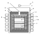
- FIG. 1 is a flowchart showing a method for manufacturing a silicon carbide single crystal according to the first embodiment of the present invention.
- FIG. 2 is a schematic cross-sectional view of an SiC manufacturing apparatus capable of implementing the method for manufacturing a silicon carbide single crystal according to the first embodiment of the present invention.
- the SiC manufacturing apparatus 1 penetrates the growth container 4 that contains the seed substrate (seed wafer) 2 and the solid silicon carbide raw material 3, the heat insulation container 5 that surrounds the growth container 4, and the heat insulation container 5.
- a temperature measuring sensor 7 for measuring the temperature in the growth vessel 4, a heater (high-frequency heating coil) 8 for heating the solid silicon carbide raw material 3, and an outer vessel for housing the heat insulating vessel 5. 9 and.
- Ta powder, carbon powder, and the like are first formed on the surface of the solid silicon carbide raw material 3 in the growth vessel 4 as shown in FIG. Then, the phenolic resin is mixed and adhered, and the seed substrate (seed wafer) 2 is placed in the upper part of the growth vessel 4.
- the phenol resin By mixing the phenol resin, Ta powder and carbon powder can be easily and uniformly attached to the surface of the solid raw material.
- the solid silicon carbide raw material 3 melt
- the growth vessel 4 is placed in the heat insulation vessel 5.
- the outer container 9 is made of, for example, SUS, quartz, or the like.
- the inside of the outer container 9 is evacuated, and the temperature is raised while maintaining a predetermined pressure.
- the inside of the external container 9 can be an argon atmosphere, a nitrogen atmosphere, or the like.
- the temperature is preferably 2000 ° C. or higher and the pressure is preferably 100 Torr (133 hPa) or lower.
- a SiC single crystal (growth crystal) 2a is grown by a sublimation method.
- the material attached to the surface of the solid silicon carbide raw material 3 is sintered, and a tantalum carbide (TaC) film 10 is formed on the surface of the solid silicon carbide raw material 3 (see FIG. 2).
- the grown silicon carbide crystal can have a reduced carbon inclusion.
- FIG. 3 is a flowchart showing a method for manufacturing a silicon carbide single crystal according to the second embodiment of the present invention.
- FIG. 4 is a schematic cross-sectional view of an SiC manufacturing apparatus that can implement the method for manufacturing a silicon carbide single crystal according to the second embodiment of the present invention. 4 has the same configuration as that of SiC manufacturing apparatus 1 in FIG.
- the method for producing a silicon carbide single crystal according to the second embodiment of the present invention first, as shown in FIG. 3A, on the surface of the solid silicon carbide raw material 3 in the growth vessel 4 and the side wall of the growth vessel 4, Ta powder, carbon powder, and phenol resin are mixed and adhered.
- sintering is performed at a high temperature, and the deposited material is converted into a TaC film and cooled.
- a tantalum carbide film 10 is formed on the surface of the solid silicon carbide raw material 3, and a tantalum carbide film 10 'is also formed on the side wall of the growth vessel 4 (see FIG. 4).
- seed substrate (seed wafer) 2 is set on the growth vessel 4 as shown in FIG.
- the growth vessel 4 is placed in the heat insulation vessel 5.
- the heat insulating container 5 is placed in the outer container 9.
- the inside of the outer container 9 is evacuated, and the temperature is raised while maintaining a predetermined pressure.
- the inside of the external container 9 can be an argon atmosphere, a nitrogen atmosphere, or the like.
- the temperature is preferably 2000 ° C. or higher and the pressure is preferably 100 Torr (133 hPa) or lower.
- the SiC single crystal (growth crystal) 2a is grown by the sublimation method.
- the silicon carbide single crystal is grown, so that a lump of carbon is formed from the solid raw material. Carbon is prevented from floating, and the carbon in the growth vessel reacts to prevent carbon from entering the growing single crystal.
- the silicon crystal can have a more effectively reduced carbon inclusion.
- a TaC film is also formed on the inner wall of the growth vessel. However, as long as the TaC film is formed on the surface of the solid silicon carbide raw material, it is not always necessary to form it on the surface of the forming vessel. Absent. However, carbon inclusion can be further suppressed by growing the growth vessel on the inner wall.
- Example 1 A SiC single crystal having a diameter of 4 inches (100 mm) was grown under the following growth conditions. ⁇ Conditions> Seed crystal substrate: growth temperature of SiC single crystal substrate with a diameter of 4 inches (100 mm) inclined by 4 ° in the ⁇ 1120> direction from the ⁇ 0001 ⁇ plane: 2200 ° C. Pressure: 10 Torr (13 hPa) Atmosphere: Argon gas, Nitrogen gas A SiC single crystal was manufactured by the procedure shown in FIG. 1 (that is, the procedure described in the first embodiment).
- Example 1 The produced single crystal was cut out, and the distribution and average number (density) of carbon inclusions in the wafer surface were examined with a microscope. The result is shown in FIG. As can be seen from FIG. 5, in Example 1, the carbon inclusion density is 2.4 / cm 2 , and it can be seen that the carbon inclusion is greatly improved as compared with the comparative example described later.
- Example 2 A SiC single crystal having a diameter of 4 inches (100 mm) was grown under the following growth conditions. ⁇ Conditions> Seed crystal substrate: growth temperature of SiC single crystal substrate with a diameter of 4 inches (100 mm) inclined by 4 ° in the ⁇ 1120> direction from the ⁇ 0001 ⁇ plane: 2200 ° C. Pressure: 10 Torr (13 hPa) Atmosphere: Argon gas, Nitrogen gas A SiC single crystal was produced by the procedure shown in FIG. 3 (ie, the procedure described in the second embodiment).
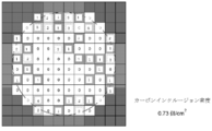
- Example 2 The produced single crystal was cut out, and the distribution and average number (density) of carbon inclusions in the wafer surface were examined with a microscope. The result is shown in FIG. As can be seen from FIG. 6, in Example 2, the carbon inclusion density is 0.73 / cm 2 , and it can be seen that the carbon inclusion is greatly improved as compared with the comparative example described later. Moreover, in Example 2, it turns out that the carbon inclusion is improved more compared with Example 1.
- FIG. 6 the carbon inclusion density is 0.73 / cm 2 , and it can be seen that the carbon inclusion is greatly improved as compared with the comparative example described later. Moreover, in Example 2, it turns out that the carbon inclusion is improved more compared with Example 1.
- SiC single crystal having a diameter of 4 inches (100 mm) was grown under the following growth conditions. ⁇ Conditions> Seed crystal substrate: growth temperature of SiC single crystal substrate with a diameter of 4 inches (100 mm) inclined by 4 ° in the ⁇ 1120> direction from the ⁇ 0001 ⁇ plane: 2200 ° C. Pressure: 10 Torr (13 hPa) Atmosphere: Argon gas, Nitrogen gas A SiC single crystal was produced according to the procedure shown in FIG.
- the produced single crystal was cut out, and the distribution and average number (density) of carbon inclusions in the wafer surface were examined with a microscope. The result is shown in FIG. As can be seen from FIG. 7, in the comparative example, the carbon inclusion density is 25.6 / cm 2 , and it can be seen that carbon inclusions are generated much more than in Examples 1 and 2.
- the present invention is not limited to the above embodiment.
- the above-described embodiment is an exemplification, and the present invention has substantially the same configuration as the technical idea described in the claims of the present invention, and any device that exhibits the same function and effect is the present invention. It is included in the technical scope of the invention.
Landscapes
- Chemical & Material Sciences (AREA)
- Engineering & Computer Science (AREA)
- Crystallography & Structural Chemistry (AREA)
- Materials Engineering (AREA)
- Metallurgy (AREA)
- Organic Chemistry (AREA)
- Inorganic Chemistry (AREA)
- Crystals, And After-Treatments Of Crystals (AREA)
- Physical Vapour Deposition (AREA)
Abstract
Description
しかしながら、SiCの結晶成長は、昇華させるために高温が必要で、成長装置は高温での温度制御が必要とされる。また、昇華した物質の圧力を安定させるために、容器内の圧力の安定した制御が必要とされる。またSiCの結晶成長は、昇華速度によるもので、Siのチョクラルスキー法やGaAsなどのLPE製法などと比較して、相対的にかなり成長速度が遅い。したがって、長い時間をかけて成長する。幸いに、昨今の制御機器の発達、コンピュータ、パソコン等の発達で、圧力、温度の調節を長期間安定して行うことが可能である。
実際には、成長容器104の下部に固体炭化珪素原材料103が配置されている。これは固体であり、高温下、減圧下で昇華する。昇華した材料は、対向する種結晶102上に単結晶として成長する。SiCの場合であれば単結晶というのは、立方晶、六方晶などがあり、更に六方晶の中でも、4H、6Hなどが、代表的なポリタイプとして知られている。
多くの場合は、4H種上には4Hが成長するというように同じタイプの単結晶が成長する(特許文献2)。
図8(a)に示すように固体炭化珪素原材料103と種基板(種ウェーハ)102を成長容器104内に配置する。次に図8(b)に示すように成長容器104を断熱容器105内に配置する。次に図8(c)に示すように断熱容器105ごと外部容器(SUS、石英等からなる)109に配置する。次に図8(d)に示すように外部容器109内を真空引きし、所定の圧力に保ちつつ、昇温する。次に図8(e)に示すように昇華法によりSiC単結晶の成長を行う。最後に図8(f)に示すように減圧圧力を上げて昇華を止め、成長を停止し、温度を徐々に下げて冷却する。
このような
以下に、本発明の第一の実施形態の炭化珪素単結晶の製造方法について、図1、2を参照しながら説明する。
図1は、本発明の第一の実施形態の炭化珪素単結晶の製造方法を示すフローチャートである。図2は本発明の第一の実施形態の炭化珪素単結晶の製造方法を実施することができるSiC製造装置の概略断面図である。
なお、固体炭化珪素原材料3は、SiC粉末を溶かして冷却し、ブロック状になったものである。
次に、本発明の第二の実施形態の炭化珪素単結晶の製造方法について、図3、4を参照しながら説明する。
図3は、本発明の第二の実施形態の炭化珪素単結晶の製造方法を示すフローチャートである。図4は、本発明の第二の実施形態の炭化珪素単結晶の製造方法を実施することができるSiC製造装置の概略断面図である。図4のSiC製造装置1’は、図2のSiC製造装置1と同様の構成を有している。
なお、この第二の実施形態において、成長容器内壁にもTaCの皮膜を形成したが、固体炭化珪素原材料の表面にTaCの皮膜を形成しさえすれば、形成容器表面には必ずしも形成する必要はない。ただし、成長容器内壁にも成長させた方がよりカーボンのインクルージョンを抑制できる。
以下の成長条件で直径4インチ(100mm)のSiC単結晶を成長させた。
<条件>
種結晶基板・・・主面が{0001}面から<1120>方向に4°傾いた直径4インチ(100mm)のSiC単結晶基板
成長温度・・・2200℃
圧力・・・10Torr(13hPa)
雰囲気・・・アルゴンガス、窒素ガス
図1に示すような手順(すなわち、第一の実施形態で説明した手順)でSiC単結晶を製造した。
以下の成長条件で直径4インチ(100mm)のSiC単結晶を成長させた。
<条件>
種結晶基板・・・主面が{0001}面から<1120>方向に4°傾いた直径4インチ(100mm)のSiC単結晶基板
成長温度・・・2200℃
圧力・・・10Torr(13hPa)
雰囲気・・・アルゴンガス、窒素ガス
図3に示すような手順(すなわち、第二の実施形態で説明した手順)でSiC単結晶を製造した。
以下の成長条件で直径4インチ(100mm)のSiC単結晶を成長させた。
<条件>
種結晶基板・・・主面が{0001}面から<1120>方向に4°傾いた直径4インチ(100mm)のSiC単結晶基板
成長温度・・・2200℃
圧力・・・10Torr(13hPa)
雰囲気・・・アルゴンガス、窒素ガス
図8に示すような手順でSiC単結晶を製造した。
Claims (2)
- 成長容器内で固体炭化珪素原材料を昇華させて種結晶基板上に炭化珪素単結晶を成長させる炭化珪素単結晶の製造方法であって、
タンタル(Ta)の粉末をカーボンの粉末とともに混合し、前記成長容器内の前記固体炭化珪素原材料に付着させ、熱処理を行い焼結し、前記固体炭化珪素原材料の表面に炭化タンタル(TaC)の皮膜を形成した後、または形成しながら炭化珪素単結晶を成長させることを特徴とする炭化珪素単結晶の製造方法。 - 前記成長容器はカーボンからなり、
前記成長容器の内壁にもタンタル(Ta)の粉末をカーボンの粉末とともに混合したものを付着させることを特徴とする請求項1に記載の炭化珪素単結晶の製造方法。
Priority Applications (4)
| Application Number | Priority Date | Filing Date | Title |
|---|---|---|---|
| EP19764126.9A EP3763853A4 (en) | 2018-03-08 | 2019-02-14 | MANUFACTURING PROCESS FOR A SILICON CARBIDE SINGLE CRYSTAL |
| US16/978,813 US20210047748A1 (en) | 2018-03-08 | 2019-02-14 | Method for manufacturing silicon carbide single crystal |
| KR1020207024691A KR20200128007A (ko) | 2018-03-08 | 2019-02-14 | 탄화규소 단결정의 제조방법 |
| CN201980017792.4A CN111819311A (zh) | 2018-03-08 | 2019-02-14 | 碳化硅单晶的制造方法 |
Applications Claiming Priority (2)
| Application Number | Priority Date | Filing Date | Title |
|---|---|---|---|
| JP2018-042289 | 2018-03-08 | ||
| JP2018042289A JP6881357B2 (ja) | 2018-03-08 | 2018-03-08 | 炭化珪素単結晶の製造方法 |
Publications (1)
| Publication Number | Publication Date |
|---|---|
| WO2019171901A1 true WO2019171901A1 (ja) | 2019-09-12 |
Family
ID=67846099
Family Applications (1)
| Application Number | Title | Priority Date | Filing Date |
|---|---|---|---|
| PCT/JP2019/005388 Ceased WO2019171901A1 (ja) | 2018-03-08 | 2019-02-14 | 炭化珪素単結晶の製造方法 |
Country Status (7)
| Country | Link |
|---|---|
| US (1) | US20210047748A1 (ja) |
| EP (1) | EP3763853A4 (ja) |
| JP (1) | JP6881357B2 (ja) |
| KR (1) | KR20200128007A (ja) |
| CN (1) | CN111819311A (ja) |
| TW (1) | TWI774929B (ja) |
| WO (1) | WO2019171901A1 (ja) |
Cited By (2)
| Publication number | Priority date | Publication date | Assignee | Title |
|---|---|---|---|---|
| US11111599B2 (en) * | 2018-09-06 | 2021-09-07 | Showa Denko K.K. | Single crystal growth method which includes covering a part of a surface of a raw material for sublimation with a metal carbide powder |
| US11814749B2 (en) | 2018-09-06 | 2023-11-14 | Resonac Corporation | Single crystal growth crucible and single crystal growth method |
Families Citing this family (4)
| Publication number | Priority date | Publication date | Assignee | Title |
|---|---|---|---|---|
| JP7258273B2 (ja) * | 2018-09-06 | 2023-04-17 | 株式会社レゾナック | SiC単結晶の製造方法及び被覆部材 |
| KR102523343B1 (ko) * | 2021-11-05 | 2023-04-19 | 주식회사 쎄닉 | 탄화규소 웨이퍼의 제조방법 및 탄화규소 잉곳의 제조방법 |
| CN114657632B (zh) * | 2022-02-24 | 2023-12-12 | 北京粤海金半导体技术有限公司 | 钽制结构、测温孔结构、坩埚组件、测温孔防堵方法 |
| CN115787077A (zh) * | 2022-12-12 | 2023-03-14 | 湖南三安半导体有限责任公司 | 用于坩埚的过滤材料、坩埚及过滤材料制备方法 |
Citations (4)
| Publication number | Priority date | Publication date | Assignee | Title |
|---|---|---|---|---|
| JPH11116399A (ja) * | 1997-10-16 | 1999-04-27 | Denso Corp | 炭化タンタルのコーティング方法及びこの方法を用いて製造した単結晶製造装置 |
| JP2000191399A (ja) | 1998-12-25 | 2000-07-11 | Showa Denko Kk | 炭化珪素単結晶およびその製造方法 |
| JP2005239465A (ja) | 2004-02-25 | 2005-09-08 | Matsushita Electric Ind Co Ltd | 炭化珪素単結晶製造装置 |
| CN105734671A (zh) * | 2014-12-10 | 2016-07-06 | 北京天科合达半导体股份有限公司 | 一种高质量碳化硅晶体生长的方法 |
Family Cites Families (5)
| Publication number | Priority date | Publication date | Assignee | Title |
|---|---|---|---|---|
| JPH09268096A (ja) * | 1996-03-29 | 1997-10-14 | Toyota Central Res & Dev Lab Inc | 単結晶の製造方法及び種結晶 |
| CN104246023B (zh) * | 2012-04-20 | 2019-02-01 | 贰陆股份公司 | 大直径高品质的SiC单晶、方法和设备 |
| WO2016133220A1 (ja) * | 2015-02-18 | 2016-08-25 | キリン株式会社 | 発熱体及びその製造方法 |
| CN107815683A (zh) * | 2016-04-22 | 2018-03-20 | 宁波高新区夏远科技有限公司 | 一种不粘锅及其制备方法 |
| CN106699228A (zh) * | 2016-12-19 | 2017-05-24 | 北京世纪金光半导体有限公司 | 一种低成本碳化钽涂层的制备方法 |
-
2018
- 2018-03-08 JP JP2018042289A patent/JP6881357B2/ja not_active Expired - Fee Related
-
2019
- 2019-02-14 CN CN201980017792.4A patent/CN111819311A/zh active Pending
- 2019-02-14 EP EP19764126.9A patent/EP3763853A4/en active Pending
- 2019-02-14 WO PCT/JP2019/005388 patent/WO2019171901A1/ja not_active Ceased
- 2019-02-14 US US16/978,813 patent/US20210047748A1/en not_active Abandoned
- 2019-02-14 KR KR1020207024691A patent/KR20200128007A/ko not_active Ceased
- 2019-02-22 TW TW108105921A patent/TWI774929B/zh active
Patent Citations (4)
| Publication number | Priority date | Publication date | Assignee | Title |
|---|---|---|---|---|
| JPH11116399A (ja) * | 1997-10-16 | 1999-04-27 | Denso Corp | 炭化タンタルのコーティング方法及びこの方法を用いて製造した単結晶製造装置 |
| JP2000191399A (ja) | 1998-12-25 | 2000-07-11 | Showa Denko Kk | 炭化珪素単結晶およびその製造方法 |
| JP2005239465A (ja) | 2004-02-25 | 2005-09-08 | Matsushita Electric Ind Co Ltd | 炭化珪素単結晶製造装置 |
| CN105734671A (zh) * | 2014-12-10 | 2016-07-06 | 北京天科合达半导体股份有限公司 | 一种高质量碳化硅晶体生长的方法 |
Non-Patent Citations (1)
| Title |
|---|
| See also references of EP3763853A4 |
Cited By (2)
| Publication number | Priority date | Publication date | Assignee | Title |
|---|---|---|---|---|
| US11111599B2 (en) * | 2018-09-06 | 2021-09-07 | Showa Denko K.K. | Single crystal growth method which includes covering a part of a surface of a raw material for sublimation with a metal carbide powder |
| US11814749B2 (en) | 2018-09-06 | 2023-11-14 | Resonac Corporation | Single crystal growth crucible and single crystal growth method |
Also Published As
| Publication number | Publication date |
|---|---|
| US20210047748A1 (en) | 2021-02-18 |
| CN111819311A (zh) | 2020-10-23 |
| JP6881357B2 (ja) | 2021-06-02 |
| EP3763853A4 (en) | 2021-12-01 |
| JP2019156660A (ja) | 2019-09-19 |
| EP3763853A1 (en) | 2021-01-13 |
| TWI774929B (zh) | 2022-08-21 |
| TW201938855A (zh) | 2019-10-01 |
| KR20200128007A (ko) | 2020-11-11 |
Similar Documents
| Publication | Publication Date | Title |
|---|---|---|
| WO2019171901A1 (ja) | 炭化珪素単結晶の製造方法 | |
| JP5304792B2 (ja) | SiC単結晶膜の製造方法および装置 | |
| KR101960209B1 (ko) | 탄화규소 단결정 잉곳의 제조 방법 및 탄화규소 단결정 잉곳 | |
| US20150361580A1 (en) | Device and method for producing multi silicon carbide crystals | |
| JP6813779B2 (ja) | 単結晶製造装置及び単結晶製造方法 | |
| JP4830073B2 (ja) | 炭化珪素単結晶の成長方法 | |
| KR102631661B1 (ko) | 탄화규소 단결정의 제조방법 | |
| JP5602093B2 (ja) | 単結晶の製造方法および製造装置 | |
| JP2006290635A (ja) | 炭化珪素単結晶の製造方法及び炭化珪素単結晶インゴット | |
| JP5761264B2 (ja) | SiC基板の製造方法 | |
| KR102767718B1 (ko) | 탄화규소의 성장 방법, 탄화규소의 성장 장치 및 이를 이용하여 성장된 탄화규소 단결정 | |
| WO2010082574A1 (ja) | 窒化物半導体結晶の製造方法、窒化物半導体結晶および窒化物半導体結晶の製造装置 | |
| KR102670425B1 (ko) | 탄화규소 단결정의 제조방법 및 제조장치 | |
| JP5573753B2 (ja) | SiC成長装置 | |
| WO2019176446A1 (ja) | 炭化珪素単結晶の製造方法 | |
| JP7707913B2 (ja) | SiC単結晶インゴットの製造方法 | |
| JP2007112661A (ja) | 炭化ケイ素単結晶の製造方法及び製造装置 | |
| WO2019130873A1 (ja) | 炭化珪素単結晶の製造方法 | |
| KR20200066491A (ko) | 대구경 단결정 성장장치 및 대구경 단결정 성장방법 |
Legal Events
| Date | Code | Title | Description |
|---|---|---|---|
| 121 | Ep: the epo has been informed by wipo that ep was designated in this application |
Ref document number: 19764126 Country of ref document: EP Kind code of ref document: A1 |
|
| ENP | Entry into the national phase |
Ref document number: 20207024691 Country of ref document: KR Kind code of ref document: A |
|
| NENP | Non-entry into the national phase |
Ref country code: DE |
|
| WWE | Wipo information: entry into national phase |
Ref document number: 2019764126 Country of ref document: EP |
|
| ENP | Entry into the national phase |
Ref document number: 2019764126 Country of ref document: EP Effective date: 20201008 |