WO2019172323A1 - 感知センサ - Google Patents
感知センサ Download PDFInfo
- Publication number
- WO2019172323A1 WO2019172323A1 PCT/JP2019/008897 JP2019008897W WO2019172323A1 WO 2019172323 A1 WO2019172323 A1 WO 2019172323A1 JP 2019008897 W JP2019008897 W JP 2019008897W WO 2019172323 A1 WO2019172323 A1 WO 2019172323A1
- Authority
- WO
- WIPO (PCT)
- Prior art keywords
- oscillation circuit
- temperature
- base body
- substrate
- piezoelectric vibrator
- Prior art date
- Legal status (The legal status is an assumption and is not a legal conclusion. Google has not performed a legal analysis and makes no representation as to the accuracy of the status listed.)
- Ceased
Links
Images


Classifications
-
- G—PHYSICS
- G01—MEASURING; TESTING
- G01N—INVESTIGATING OR ANALYSING MATERIALS BY DETERMINING THEIR CHEMICAL OR PHYSICAL PROPERTIES
- G01N29/00—Investigating or analysing materials by the use of ultrasonic, sonic or infrasonic waves; Visualisation of the interior of objects by transmitting ultrasonic or sonic waves through the object
- G01N29/02—Analysing fluids
- G01N29/036—Analysing fluids by measuring frequency or resonance of acoustic waves
-
- G—PHYSICS
- G01—MEASURING; TESTING
- G01N—INVESTIGATING OR ANALYSING MATERIALS BY DETERMINING THEIR CHEMICAL OR PHYSICAL PROPERTIES
- G01N29/00—Investigating or analysing materials by the use of ultrasonic, sonic or infrasonic waves; Visualisation of the interior of objects by transmitting ultrasonic or sonic waves through the object
- G01N29/02—Analysing fluids
- G01N29/022—Fluid sensors based on microsensors, e.g. quartz crystal-microbalance [QCM], surface acoustic wave [SAW] devices, tuning forks, cantilevers, flexural plate wave [FPW] devices
-
- G—PHYSICS
- G01—MEASURING; TESTING
- G01N—INVESTIGATING OR ANALYSING MATERIALS BY DETERMINING THEIR CHEMICAL OR PHYSICAL PROPERTIES
- G01N29/00—Investigating or analysing materials by the use of ultrasonic, sonic or infrasonic waves; Visualisation of the interior of objects by transmitting ultrasonic or sonic waves through the object
- G01N29/22—Details, e.g. general constructional or apparatus details
- G01N29/222—Constructional or flow details for analysing fluids
-
- G—PHYSICS
- G01—MEASURING; TESTING
- G01N—INVESTIGATING OR ANALYSING MATERIALS BY DETERMINING THEIR CHEMICAL OR PHYSICAL PROPERTIES
- G01N29/00—Investigating or analysing materials by the use of ultrasonic, sonic or infrasonic waves; Visualisation of the interior of objects by transmitting ultrasonic or sonic waves through the object
- G01N29/22—Details, e.g. general constructional or apparatus details
- G01N29/24—Probes
- G01N29/2437—Piezoelectric probes
- G01N29/2443—Quartz crystal probes
-
- G—PHYSICS
- G01—MEASURING; TESTING
- G01N—INVESTIGATING OR ANALYSING MATERIALS BY DETERMINING THEIR CHEMICAL OR PHYSICAL PROPERTIES
- G01N29/00—Investigating or analysing materials by the use of ultrasonic, sonic or infrasonic waves; Visualisation of the interior of objects by transmitting ultrasonic or sonic waves through the object
- G01N29/22—Details, e.g. general constructional or apparatus details
- G01N29/32—Arrangements for suppressing undesired influences, e.g. temperature or pressure variations, compensating for signal noise
- G01N29/323—Arrangements for suppressing undesired influences, e.g. temperature or pressure variations, compensating for signal noise compensating for pressure or tension variations
-
- G—PHYSICS
- G01—MEASURING; TESTING
- G01N—INVESTIGATING OR ANALYSING MATERIALS BY DETERMINING THEIR CHEMICAL OR PHYSICAL PROPERTIES
- G01N29/00—Investigating or analysing materials by the use of ultrasonic, sonic or infrasonic waves; Visualisation of the interior of objects by transmitting ultrasonic or sonic waves through the object
- G01N29/22—Details, e.g. general constructional or apparatus details
- G01N29/32—Arrangements for suppressing undesired influences, e.g. temperature or pressure variations, compensating for signal noise
- G01N29/326—Arrangements for suppressing undesired influences, e.g. temperature or pressure variations, compensating for signal noise compensating for temperature variations
-
- G—PHYSICS
- G01—MEASURING; TESTING
- G01N—INVESTIGATING OR ANALYSING MATERIALS BY DETERMINING THEIR CHEMICAL OR PHYSICAL PROPERTIES
- G01N15/00—Investigating characteristics of particles; Investigating permeability, pore-volume or surface-area of porous materials
- G01N15/06—Investigating concentration of particle suspensions
- G01N15/0606—Investigating concentration of particle suspensions by collecting particles on a support
-
- G—PHYSICS
- G01—MEASURING; TESTING
- G01N—INVESTIGATING OR ANALYSING MATERIALS BY DETERMINING THEIR CHEMICAL OR PHYSICAL PROPERTIES
- G01N2291/00—Indexing codes associated with group G01N29/00
- G01N2291/02—Indexing codes associated with the analysed material
- G01N2291/025—Change of phase or condition
- G01N2291/0256—Adsorption, desorption, surface mass change, e.g. on biosensors
-
- G—PHYSICS
- G01—MEASURING; TESTING
- G01N—INVESTIGATING OR ANALYSING MATERIALS BY DETERMINING THEIR CHEMICAL OR PHYSICAL PROPERTIES
- G01N33/00—Investigating or analysing materials by specific methods not covered by groups G01N1/00 - G01N31/00
- G01N33/0095—Semiconductive materials
Definitions
- the present invention relates to a sensing sensor that senses a sensing object by changing the frequency of a piezoelectric vibrator.
- a QCM Quadrat microwave crystal microbalance
- a sensing device using a sensing sensor that senses a substance contained in a gas.
- the crystal is cooled to a cryogenic temperature to cause gas to adhere to the crystal, and then the temperature of the crystal is gradually increased to remove the gas attached to the crystal.
- a sensing device that measures the amount of adhesion of gas by measuring the amount of frequency change before and after the desorption of gas, and identifies the component of the gas by measuring the temperature at which the gas desorbs. .
- the CI crystal impedance
- the negative resistance of the oscillation circuit must be increased as much as possible.
- the semiconductor used for the oscillation circuit tends to increase its negative resistance when driven at low temperatures as its characteristics. Therefore, the oscillation circuit is cooled as much as possible by using thermal cooling such as liquid nitrogen. It is preferable that
- the temperature of the oscillation circuit is lowered, for example, a silicon semiconductor element has a tendency that the carrier density decreases from a temperature around ⁇ 110 ° C. and the insulating property increases. For this reason, if the temperature is too low, semiconductor elements such as an oscillation IC (integrated circuit) and a regulator provided in the oscillation circuit fall below the functional limit temperature, and the oscillation circuit stops. Therefore, by operating the oscillation circuit board at a temperature as low as possible that is not lower than the functional limit temperature of the semiconductor, the most negative resistance can be obtained, the measurement dynamic range can be widened, and stable oscillation can be performed.
- an oscillation IC integrated circuit
- Patent Document 1 describes a technique for cooling a crystal resonator to increase the sensitivity of a detection sensor, but is not a technique for cooling an oscillation circuit.
- Patent Document 2 describes a technique for cooling a substrate on which an IC chip is installed, but it is not a technique for cooling to an extremely low temperature, and is not a technique considering temperature characteristics of a semiconductor element.
- the present invention has been made based on such circumstances, and the object thereof is to widen the measurement dynamic range and stable detection in a sensing sensor that senses by cooling and heating a piezoelectric vibrator and desorbing and attaching a substance. It is to provide the technology to do.
- the sensing sensor of the present invention attaches a substance to be sensed, which is a gas, to the piezoelectric vibrator, changes the temperature of the piezoelectric vibrator to desorb the substance to be sensed, and changes the oscillation frequency of the piezoelectric vibrator and the temperature.
- a substance to be sensed which is a gas
- the sensing sensor that senses the substance to be sensed based on the relationship with A base body cooled by liquid nitrogen; A piezoelectric vibrator cooled by the base body; A heating unit for heating the piezoelectric vibrator in order to change the temperature of the piezoelectric vibrator; An oscillation circuit unit that is attached to the base body and oscillates the piezoelectric vibrator, and a substrate on which a heater circuit for heating the oscillation circuit unit is mounted; In order to prevent cold heat from being transferred from the base body to the oscillation circuit section through the substrate, a heat insulating section provided between the base body and the oscillation circuit section is provided. .
- the present invention attaches a substance to be sensed that is a gas to a piezoelectric vibrator, changes the temperature of the piezoelectric vibrator to desorb the substance to be sensed, and relates the relationship between the change in the oscillation frequency of the piezoelectric vibrator and the temperature.
- the piezoelectric vibrator is cooled by the base body cooled by liquid nitrogen and heated by the heating unit.
- the base body is provided with an oscillation circuit section for oscillating the piezoelectric vibrator and a substrate on which a heater circuit for heating the oscillation circuit section is mounted, and a heat insulating section provided between the base body and the oscillation circuit section is provided.
- the temperature of the oscillation circuit can be kept as low as possible without falling below the functional limit temperature of the oscillation circuit. Therefore, the negative resistance of the oscillation circuit is increased, the measurement dynamic range can be widened, and stable oscillation can be performed.
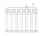
- sensing sensor It is a disassembled perspective view of the sensing sensor which concerns on embodiment of this invention. It is a longitudinal cross-sectional view of the sensing sensor which concerns on embodiment of this invention. It is the top view and side view which show the spacer used for a sensing sensor. It is a top view which shows the surface side and back surface side of the crystal oscillator used for a sensing sensor. It is a top view which shows the sensor board
- the detection sensor 1 includes a cylindrical lid portion 10 whose lower side is open, and a base body 20 that closes the lower portion of the lid portion 10.
- the base body 20 is formed in a disk shape from, for example, nickel-plated copper, and a planar circular protrusion 21 is formed at the center of one surface side (upper surface side).
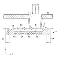
- a planar rectangular recess 22 is formed in the projecting portion 21, and an oscillation circuit board 3 described later is supported at both ends in the X direction in FIG. 1 at the bottom of the recess 22 as shown in FIG.
- Each step 23 is formed. Further, as shown in FIG.
- a hole 203 into which a cable 38 a connected to a connector 38 described later is inserted is formed at the bottom of the recess 22.
- holes 26 into which pins 43a and 43b described later are inserted are formed at positions corresponding to the pins 43a and 43b.
- liquid nitrogen is used as the refrigerant.
- the oscillation circuit board 3 is disposed inside the recess 22.
- the oscillation circuit board 3 is an IC (integrated IC) which is a silicon semiconductor element on which an oscillation circuit and an oscillation circuit section such as a regulator are mounted on the front surface side and the back surface side of the substrate 30, respectively.
- a circuit area 31 in which a circuit) is stored is provided.
- four cylindrical sockets 32 and 33 for electrical connection with ICs in the circuit area 31 are arranged side by side at both ends of the substrate 30 in the X direction.
- holes 30a communicating with the sockets 32 and 33 are formed at positions corresponding to the sockets 32 and 34 on the substrate 30, respectively.
- a cable 38 a for electrically connecting the connector 38 and the IC in the circuit area 31 is connected to the lower end of the end portion on one side in the Y-axis direction of the oscillation circuit board 3.
- the cable 38 a and the connector 38 are connected, but the connector 38 is disposed on the lower surface side of the base body 20.
- the oscillation circuit board 3 is provided in the recess 22 via the spacer 9.
- the spacer 9 is made of a plate-like body having a thickness of 0.5 mm made of, for example, Teflon (registered trademark), and an X-shaped through-hole portion 90 penetrating in the thickness direction is formed.
- the through-hole portion 90 is provided at a position corresponding to the six hole portions 30 a formed at the X-direction end portion of the substrate 30.
- the spacer 9 is arranged on the upper surface of each step portion 23 so that the positions of the through hole portion 90 and the hole portion 26 are aligned, and the oscillation circuit board 3 is arranged so that the six hole portions 30 a are aligned with the through hole portion 90. Be placed.
- a circuit area 31 on the oscillation circuit board 3 and an outer area spaced from an area where elements such as switches 60 and 61 and a heater resistor 64 described later are provided are positioned above the spacer 9.
- a guide member 34 for guiding the sockets 32 and 33 is provided above the oscillation circuit board 3.
- the guide member 34 is formed with a through hole 34 a for guiding the sockets 32 and 33.
- a plate-like member 36 is provided above the guide 34.
- the plate-like member 36 is configured such that holes 37 are provided at both ends 36a in the Y-axis direction so that the region between the both ends 36a extends in the X-axis direction.
- the plate member 36 is pressed against the guide 34 from the Z-axis direction, and both end portions 36a of the plate member 36 in the Y direction shown in FIG. It is fixed to the upper surface of the protrusion 21.
- the guide member 34, the oscillation circuit board 3, and the spacer 9 are fixed inside the recess 22.
- the crystal unit 5 includes a disk-shaped crystal piece 50 that is, for example, an AT-cut piezoelectric piece.
- a pair of first excitation electrodes (reaction electrodes) 51 made of, for example, gold (Au) or the like, respectively.
- an extraction electrode 55, 56 is connected to the first and second excitation electrodes 51, 52 on the upper surface side, respectively, and the extraction electrode 55, 56 is routed around the side surface of the crystal piece 50, and the lower surface Terminal portions 55a and 56a are formed at the peripheral edge portion.
- One end of each of the extraction electrodes 57 and 58 is connected to the first and second excitation electrodes 53 and 54 on the lower surface side.
- the extraction electrodes 57 and 58 have terminal portions 57a and 58a at the peripheral portions. Is formed.
- the sensor substrate 4 includes a substantially rectangular substrate 40 as a support member.
- an oval recess 40 a is formed at a position corresponding to the first and second excitation electrodes 53 and 54 on the lower surface side formed on the crystal resonator 5.
- wirings 44, 45, 46, and 47 are provided at positions corresponding to the terminal portions 55a, 56a, 57a, and 58a formed on the lower surface of the crystal resonator 5, respectively. As shown in FIG.
- conductive pins 43 a extend toward the lower side at a position corresponding to the socket 32 of the oscillation circuit board 3 on one end side in the X-axis direction on the lower surface side of the sensor board 4. Yes. Further, on the other end side in the X-axis direction on the lower surface side of the sensor substrate 4, four conductive pins 43 b extend toward the lower side at a position corresponding to the socket 33 of the oscillation circuit substrate 3.
- Each wiring 44, 45, 46, 47 shown in FIG. 5 is routed to the lower surface side through the side surface of the substrate 40, and is connected to the pin 43a.
- a heating unit 49 configured by, for example, a heating resistor for heating the crystal unit 5 is embedded in the substrate 40 of the sensor substrate 4. Further, the sensor substrate 4 is provided with a temperature detection unit 41 for detecting the temperature of the crystal unit 5. The heating unit 49 and the temperature detection unit 41 are routed to the lower surface side of the substrate 40 through the wiring 42 and the through hole 42a and connected to the pin 43b. Further, holes 48 are respectively formed at positions corresponding to the fixing members 25 of the respective struts 24 on the peripheral edge in the Y-axis direction of the substrate 40. As shown in FIG.
- the sensor substrate 4 is positioned in the X-axis direction and the Y-axis direction by inserting the fixing member 25 into each hole 48, and the substrate 40 is placed on the upper surface of the column 24.
- the height position is fixed as shown in FIG.
- the pins 43 and 44 are inserted into the through holes 34a of the guide member 34 and inserted into the corresponding sockets 32 and 33, respectively.
- the pins 43a are electrically connected when inserted into the sockets 32, respectively.
- the tip of the pin 43a is inserted into the hole 30a formed in the substrate 30 and the through hole 90 formed in the spacer 9, and is inserted into the hole 26 formed in the step portion 23, respectively.
- the cable 38 a connected to the oscillation circuit board 3 is routed below the base body through the hole 203 formed in the base body 20 and connected to the connector 38.
- the crystal resonator 5 provided on the substrate 40, the circuit area 31, and the connector 38 are electrically connected to each other.
- the lid portion 10 is disposed so as to cover the upper side of the sensor substrate 4 and surround the periphery of the protruding portion 21, and the lid portion 10 and the base body 20. Are engaged.
- a mortar-shaped opening 11 is formed at a position near the one end side in the Y-axis direction on the upper surface of the lid 10 as shown in FIG.
- the first excitation electrode 51 on the upper surface side of the crystal resonator 5 faces the opening 11. At this time, the lower end of the opening 11 is separated from the surface of the crystal unit 5 by 0.5 mm.
- the oscillation circuit board 3 is provided with an oscillation circuit 62 configured in each circuit area 31 and a regulator 63 for adjusting a voltage supplied to the oscillation circuit 62.
- the oscillation circuit 62 and the regulator 63 correspond to the oscillation circuit unit 6.
- the first and second excitation electrodes 51 and 52 on the upper surface side of the crystal resonator 5 are connected via the switch 60 provided on the oscillation circuit substrate 3.
- the first and second excitation electrodes 53 and 54 on the lower surface side of the crystal unit 5 are connected to the oscillation circuit 62 via the switch 61 provided on the oscillation circuit substrate 3.
- the detection sensor 1 is connected to the main body portion 7 via the connector 38.
- the main body unit 7 includes, for example, a power supply unit 70 that supplies a driving voltage to an oscillation circuit 62 provided in the sensing sensor 1, and a frequency measurement unit 71 that measures a frequency output from the oscillation circuit 62.
- the frequency signal measured by the frequency measuring unit 71 is configured to be input to the control unit 72.
- the main body unit 7 includes a temperature adjusting unit 73 that adjusts the output of the heating unit 49 based on the temperature detection value detected by the temperature detecting unit 41 to control the temperature of the crystal unit 5.
- control unit 72 can adjust the set temperature of the temperature adjustment unit 73 to increase the temperature of the crystal unit 5 from ⁇ 190 ° C., which is the temperature cooled by liquid nitrogen, at a rate of 1 ° C./1 minute. It is configured as follows.
- the power supply unit 70 is connected to the regulator 63.
- a voltage of 5V output from the power supply unit 70 is adjusted by the regulator 63 to become a voltage of 3V and is applied to the oscillation circuit 62.
- the oscillation circuit board 3 includes a heater resistor 64 having a resistance of 330 ⁇ , for example, which is a heater circuit for heating the oscillation circuit 62.
- the heater resistor 64 is connected in parallel with the regulator 63, and generates heat due to a 5 V voltage output from the power supply unit 70.
- the heater resistor 64 heats the oscillation circuit 62 and the regulator 63 (oscillation circuit unit 6) configured in the circuit area 31.
- the frequency measuring unit 71 is connected to the oscillation circuit 62.
- the sensing sensor 1 according to the present invention switches the switch 60 and the switch 61 so that the excitation electrodes connected to the oscillation circuit 62 are connected to the reaction electrode side (first excitation electrodes 51 and 53) and the reference electrode side (second excitation). Switching between the electrodes 52, 54).
- the frequency measurement unit 71 measures the first oscillation frequency F1 on the reaction electrode side and the second oscillation frequency F2 on the reference electrode side.
- the control unit 72 includes the first oscillation frequency F1 of the first excitation electrodes 51 and 53 on the reaction electrode side and the second oscillation frequency F2 of the second excitation electrodes 52 and 54 on the reference electrode side, which are measured in advance. The relationship between the difference between the two and the amount (mass) of the sensing object is stored. Then, from the difference between the first oscillation frequency F1 and the second oscillation frequency F2 measured by the frequency measuring unit 71, the amount of the sensing object corresponding to the difference is detected.
- the sensing sensor 1 according to the embodiment of the present invention will be described.
- the main body 7 is connected to the connector 38 of the sensing sensor 1, and then liquid nitrogen is passed through the refrigerant flow path 200.
- the base body 20 is cooled to, for example, ⁇ 190 ° C.
- the sensor substrate 4 is cooled via the pins 43 and 44 and the column 24, and is cooled to, for example, -184 ° C. Therefore, the pins 43 and 44 and the column 24 correspond to heat transfer members.
- a gas that is a sensing object is supplied toward the opening 11 of the sensing sensor 1.
- the gas supplied at this time is cooled and attached by contacting the first excitation electrode 51 on the reaction electrode side facing the bottom of the opening 11.
- the switches 60 and 61 are switched by time division, and the control unit 72 oscillates the oscillation frequency F1 on the reaction electrode side (first excitation electrodes 51 and 53) and the oscillation on the reference electrode side (second excitation electrodes 52 and 54).
- the heating unit 49 is gradually heated at, for example, 1 ° C./1 minute.
- the crystal unit 5 is gradually heated, the sensing object attached to the first excitation electrode 51 is detached.
- the oscillation frequency F1 of the first excitation electrodes 51 and 53 on the reaction electrode side greatly changes.
- the second excitation electrodes 52 and 54 on the reference electrode side no sensing object adheres, so that no mass change occurs when the temperature is raised, and the oscillation frequency F2 hardly changes.
- the control unit 72 observes the oscillation frequencies F1 and F2 to grasp the timing of the gas desorption, and based on the difference between the first oscillation frequency F1 and the second oscillation frequency F2, the sensing object The mass of is detected.
- the temperature detection unit 41 always detects the temperature, and detects the temperature at the timing as the desorption temperature of the sensing object. Thus, the type of the sensing object can be specified based on the detected desorption temperature. In this way, the gas to be sensed is detected.
- the oscillation circuit board 3 is positioned above the Teflon spacer 9 disposed on the upper surface of the step portion 23 of the base body 20. It is supported in a sticky state.
- the heat conduction between the base body 20 and the oscillation circuit board 3 is relaxed by the spacer 9.
- the cooling temperature of the oscillation circuit board 3 and the circuit area 31 installed on the oscillation circuit board 3 is higher than the temperature of the base body 20.
- the power supply unit 70 when the power supply unit 70 is turned on, a voltage adjusted to 3 V is applied to the oscillation circuit 62 via the regulator 63. As a result, the oscillation circuit 62 is driven and the crystal unit 5 oscillates. At this time, the voltage applied from the power supply unit 70 is also applied to the heater resistor 64, and the heater resistor 64 generates heat.
- the oscillation circuit 62 has a negative resistance that is increased by lowering the temperature.
- the sensing sensor 1 of the present invention attaches the sensing object to the crystal resonator 5 as described above, and detects the sensing object based on the amount of change in the frequency. Since the CI value increases, the range of frequencies that normally oscillate becomes narrower. Therefore, from the viewpoint of widening the measurable frequency range, it is preferable to increase the negative resistance on the oscillation circuit 32 side, and it is preferable to lower the temperature.
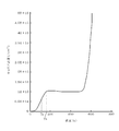
- a semiconductor element formed of silicon has different carrier densities depending on temperature as shown in FIG.
- This carrier density indicates the conductivity of the semiconductor element.
- the carrier density increases, the conductivity increases, and when the carrier density decreases, the insulation increases.
- a stable carrier density is maintained in a temperature range of ⁇ 110 ° C. (163 K) to 300 ° C. (573 K), but the temperature is lower than Tb, for example, about ⁇ 110 ° C.
- Tb for example, about ⁇ 110 ° C.
- the carrier density gradually decreases. Further, if the temperature falls below the temperature Ta at which the carrier density becomes too low, the insulating properties of the semiconductor element become too high and fall below the functional limit temperature.
- the temperature extremely low and above the functional limit temperature of the semiconductor element is lower than the temperature Tb, which is a temperature at which the carrier density decreases and the negative resistance of the oscillation circuit can be sufficiently increased, and the semiconductor element cannot maintain its function.
- the temperature is higher than the temperature Ta, specifically, about ⁇ 170 ° C. (103 K) to ⁇ 110 ° C. (163 K) in the case of a silicon semiconductor.
- the temperature of liquid nitrogen used as a cooling medium in the above-described embodiment is -196 ° C.
- the sensing sensor 1 configured in the same manner as the sensing sensor 1 shown in the above-described embodiment except that the spacer 9 and the heater resistor 64 are removed as shown in an example described later, oscillation occurs.
- the temperature of the circuit board 3 has dropped to ⁇ 184 ° C., and the oscillation circuit section 6 has stopped.
- the sensing sensor 1 shown in the above-described embodiment since the heat conduction is blocked by the spacer 9, the cooling of the oscillation circuit unit 6 is alleviated.
- the oscillation circuit 62 and the regulator 63 (oscillation circuit unit 6) provided on the oscillation circuit substrate 3 are heated.
- the circuit area 31 including the IC such as the oscillation circuit 62 and the regulator 63 is cooled to a very low temperature by liquid nitrogen, and the cooling by the spacer 9 and heating by the heater resistor 63 are combined, for example, ⁇ 160 ° C. Maintained at a moderate temperature.
- the oscillation circuit section 6 can be operated normally while the temperature of the oscillation circuit section 6 is in a cryogenic temperature range where the negative resistance of the oscillation circuit section 6 is increased, as shown in the embodiments described later. Can be adjusted to temperature.
- the temperature of the oscillation circuit unit 6 is maintained at a temperature of about ⁇ 160 ° C., and the negative resistance of the oscillation circuit unit 6 is large, so that the measurement range in frequency measurement is widened, and the sensing sensor The detection range of the sensing object in 1 is wide. Furthermore, the temperature is adjusted to a temperature range in which the oscillation circuit unit 6 oscillates normally without stopping. Therefore, when the sensing object adheres to the excitation electrode 51 on the upper surface side on the reaction electrode side, the crystal resonator 5 can be stably oscillated even when the CI value of the crystal resonator 5 increases.
- the oscillation circuit unit 6 that oscillates the crystal unit 5 and the oscillation circuit 62 are cooled to a cryogenic temperature.
- a spacer 9 is provided between the base body 20 and a heater resistor 64 for heating the oscillation circuit unit 6 on the oscillation circuit substrate 3. Therefore, the temperature of the oscillation circuit unit 6 can be made as low as possible without falling below the functional limit temperature of the silicon semiconductor. Therefore, the negative resistance of the oscillation circuit unit 6 can be increased, the measurement dynamic range can be widened, and the crystal unit 5 can be oscillated stably.
- the temperature as low as possible and not lower than the functional limit temperature is preferably ⁇ 170 ° C. to ⁇ 110 ° C. when the main material of the semiconductor element constituting the oscillation circuit section 6 is silicon.
- the sensor substrate 4 is configured to extend from the sensor substrate 4 and to make the tips of the pins 43a and 43b for establishing electrical connection with the oscillation circuit substrate 3 contact the base body 20, so that the oscillation circuit substrate 3 and the pins 43a and 43b are electrically connected.
- the contact area is reduced. Therefore, conduction of heat from the oscillation circuit board 3 side to the pins 43a and 43b can be suppressed, and the pins 43a and 43b can be cooled by the base body 20 and temperature rise of the sensor board 4 can be suppressed.
- a through hole 91 (through hole portion) is formed side by side between an installation region of the circuit area 31 of the substrate 30 used for the oscillation circuit substrate 3 and a region on the step portion 23 in the substrate 30.
- the cross-sectional area of the portion between the region side on the step portion 23 and the installation region of the circuit area 31 is reduced, heat conduction is suppressed, and the installation region of the circuit area 31 is less likely to be cooled. Can be obtained.
- the oscillation circuit board 3 shown in FIG. 11 may be used, and the spacer 9 may be provided between the step portion 23 and the oscillation circuit board 3. Further, instead of forming the through holes 91 side by side, a through hole such as a slit may be provided.
- the sensing sensor 1 shown in FIGS. 1 to 8 is used, and liquid nitrogen is passed through the base body 20 to cool it. It was driven and the temperature of the area
- An example in which the sensor was similarly configured using a sensing sensor configured in the same manner except that the heater resistor 64 was not provided was designated as Comparative Example 1. Further, a comparative sensor 2 was used which was processed in the same manner as the embodiment using the sensor configured similarly to the comparative example 1 except that the oscillator circuit board 3 was disposed on the upper surface of the step portion 23 except for the spacer 9.
- Table 1 shows this result.
- the temperature of the oscillation circuit board 3 after 10 minutes from the power-on of the oscillation circuit 62 and the oscillation circuit 10 minutes after the power-on of the oscillation circuit unit 6 in the examples and comparative examples 1 and 2 are shown. It shows whether or not the oscillation stop of the unit 6 has been confirmed.
- Table 1 As shown in Table 1, in Comparative Examples 1 and 2, the temperature of the oscillation circuit board 3 was ⁇ 170 ° C. or lower, and it was confirmed that the oscillation circuit unit 6 was stopped. On the other hand, in the example, the temperature of the oscillation circuit board 3 rose to ⁇ 164 ° C., and the stop of the oscillation circuit unit 6 was not confirmed. Therefore, according to the present invention, the temperature of the oscillation circuit unit 6 can be made as low as possible without falling below the functional limit temperature, the negative resistance of the oscillation circuit unit 6 is increased, and the measurement dynamic range is widened. I can say that.
- the temperature rise of the crystal unit 5 was measured from the start of driving of the oscillation circuit unit 6. As a result, immediately after the oscillation circuit 62 was turned on, it was ⁇ 191 ° C. and even after 10 minutes ⁇ It was 187 ° C. From this, it can be said that even when the heater resistor 64 for heating the oscillation circuit section 6 is provided, the temperature rise in the crystal unit 5 is sufficiently small and hardly affected.
Landscapes
- Physics & Mathematics (AREA)
- Chemical & Material Sciences (AREA)
- General Health & Medical Sciences (AREA)
- Life Sciences & Earth Sciences (AREA)
- Analytical Chemistry (AREA)
- Biochemistry (AREA)
- Health & Medical Sciences (AREA)
- General Physics & Mathematics (AREA)
- Immunology (AREA)
- Pathology (AREA)
- Acoustics & Sound (AREA)
- Crystallography & Structural Chemistry (AREA)
- Oscillators With Electromechanical Resonators (AREA)
Abstract
水晶振動子を用いた感知センサにおいて、測定ダイナミックレンジを広くすると共に安定した検出を行う技術を提供する。水晶振動子5を発振させる発振回路と、発振回路62を極低温に冷却するベース体20との間に、スペーサ9を設けると共に、発振回路基板3に発振回路62を加熱するためのヒータ抵抗64を設けている。そのため発振回路62の温度を、機能限界温度を下回らず、かつ極力低温とすることができる。発振回路62の負性抵抗を大きくすることができ、測定ダイナミックレンジを広くすると共に、水晶振動子5を安定して発振させることができる。
Description
本発明は、圧電振動子の周波数変化により感知対象物を感知する感知センサに関する。
例えばガス中に含まれる物質を感知する感知センサを用いた感知装置として、水晶振動子を用いたQCM(Quartz crystal microbalance)が知られている。このようなQCMとしては、例えば水晶振動子を極低温に冷却することにより水晶振動子にガスを付着させ、続いて水晶振動子の温度を徐々に上げて、水晶振動子に付着したガスを脱離させる。この時ガスの脱離前後の周波数変化量を測定することで、ガスの付着量を測定すると共に、ガスが脱離する温度を計測することでガスの成分を特定する感知装置が知られている。
ここでQCMにおいては、物質の付着により水晶振動子のCI(クリスタルインピーダンス)が高くなっていくため、測定のダイナミックレンジを少しでも大きくするために、発振回路の負性抵抗を極力大きくすることが好ましい。発振回路に用いられる半導体は、その特性として低温下で駆動させることにより、その負性抵抗が大きくなる傾向があるため、発振回路は、例えば液体窒素などの熱冷却を利用し、極力冷やした状態とすることが好ましい。
しかしながら発振回路の温度を下げたときに、例えばシリコン製の半導体素子は、-110℃付近の温度からキャリアの密度が少なくなり、絶縁性が高まる傾向にある。そのためあまりに極低温とした場合には、発振回路に設けられる発振用のIC(集積回路)やレギュレータなどの半導体素子が機能限界温度を下回ってしまい、発振回路が停止してしまう。そのため半導体の機能限界温度を下回らない温度で、極力低温にて発振回路基板を動作させることで最も負性抵抗が取れ、測定ダイナミックレンジも広く取れ、かつ安定した発振を行うことができる。
特許文献1には、水晶振動子を冷却して感知センサを高感度化する技術が記載されているが、発振回路の冷却を目的とした技術ではない。また特許文献2には、ICチップが設置される基板を冷却する技術が記載されているが、極低温に冷却する技術ではなく、半導体素子の温度特性を考慮した技術ではない。
本発明はこのような事情に基づいてなされたものであり、その目的は、圧電振動子を冷却加熱し物質を脱離付着させて感知する感知センサにおいて、測定ダイナミックレンジを広くすると共に安定した検出を行う技術を提供することにある。
本発明の感知センサは、気体である被感知物質を圧電振動子に付着させ、当該圧電振動子の温度を変化させて被感知物質を脱離させ、圧電振動子の発振周波数の変化と前記温度との関係に基づいて、被感知物質を感知する感知センサにおいて、
液体窒素により冷却されるベース体と、
前記ベース体により冷却される圧電振動子と、
前記圧電振動子の温度を変化させるために当該圧電振動子を加熱する加熱部と、
前記ベース体に取り付けられ、その上に前記圧電振動子を発振させる発振回路部及び当該発振回路部を加熱するためのヒータ回路が搭載された基板と、
前記ベース体から基板を介して発振回路部に冷熱が伝熱されることを妨げるために、前記ベース体と前記発振回路部との間に設けられた断熱部と、を備えたことを特徴とする。
液体窒素により冷却されるベース体と、
前記ベース体により冷却される圧電振動子と、
前記圧電振動子の温度を変化させるために当該圧電振動子を加熱する加熱部と、
前記ベース体に取り付けられ、その上に前記圧電振動子を発振させる発振回路部及び当該発振回路部を加熱するためのヒータ回路が搭載された基板と、
前記ベース体から基板を介して発振回路部に冷熱が伝熱されることを妨げるために、前記ベース体と前記発振回路部との間に設けられた断熱部と、を備えたことを特徴とする。
本発明は、気体である被感知物質を圧電振動子に付着させ、当該圧電振動子の温度を変化させて被感知物質を脱離させ、圧電振動子の発振周波数の変化と前記温度との関係に基づいて、被感知物質を感知する感知センサにおいて、圧電振動子を液体窒素により冷却されるベース体により冷却すると共に加熱部により加熱するように構成している。さらにベース体に圧電振動子を発振させる発振回路部及び当該発振回路部を加熱するためのヒータ回路が搭載された基板を設け、ベース体と前記発振回路部との間に設けられた断熱部を設けている。そのため発振回路の温度を、発振回路の機能限界温度を下回らず、かつ極力低温とすることができる。従って発振回路の負性抵抗が大きくなり、測定ダイナミックレンジを広くすることができると共に安定した発振を行うことができる。
本発明の感知センサ1の全体構成について、図1~図2を参照して説明する。図1に示すように感知センサ1は、下方側が開放された円筒状の蓋部10と、蓋部10の下方を塞ぐベース体20を備えている。図1、図2に示すようにベース体20は、例えばニッケル鍍金がされた銅により円板状に構成され、一面側(上面側)の中心部に平面形状円形の突出部21が形成されている。突出部21には、平面形状矩形の凹部22が形成され、凹部22の底部における図1中のX方向の両端には、図2に示すように後述の発振回路基板3を両持ち状に支持する段部23が各々形成されている。また凹部22の底部には、図2に示すように後述するコネクタ38と接続されるケーブル38aが挿入される孔部203が形成されている。段部23には、後述するピン43a、43bが挿入される孔部26が、各ピン43a、43bに対応する位置に形成されている。
また図1に示すように突出部21の上面には、X方向に2本離間して配置された支柱24が凹部22を介して、Y方向に2列並んで配置されている。支柱24の上端には、後述のセンサ基板4を固定するための固定部材25が夫々上方に向けて伸び出している。
また図2に示すようにベース体20の取り付け部201の内部には、冷媒流路200を流れた冷媒が溜まる冷媒液溜まり202が形成されている。冷媒としては、例えば液体窒素が用いられる。
また図2に示すようにベース体20の取り付け部201の内部には、冷媒流路200を流れた冷媒が溜まる冷媒液溜まり202が形成されている。冷媒としては、例えば液体窒素が用いられる。
凹部22の内部には、発振回路基板3が配置される。図1、図2に示すように発振回路基板3は、基板30の表面側及び裏面側に各々発振回路や、レギュレータなどの発振回路部、が実装されたシリコン製の半導体素子であるIC(集積回路)が収納された回路エリア31が設けられている。また基板30のX方向の両端には、回路エリア31内のICと電気的に接続するための筒状のソケット32、33が各々4つづつ並べて配置されている。また図2にしめすように基板30における各ソケット32、34に対応する位置には、各々各ソケット32、33と連通する孔部30aが形成されている。なおこの例では、ソケット32、33が配置される孔部30aが基板30のX方向両端に6か所づつ予め形成されており、ソケット32は、外側の2つづつの孔部30aに各々配置され、ソケット33は、中心寄りの4つの孔部30aに配置されている。また発振回路基板3のY軸方向一方側の端部には、下面側にコネクタ38と回路エリア31内のICとを電気的に接続させるためのケーブル38aが接続されている。なお図1ではケーブル38aとコネクタ38とを接続した図で示しているがコネクタ38はベース体20の下面側に配置される。
発振回路基板3は、スペーサ9を介して凹部22内に設けられる。スペーサ9は、図3に示すように例えばテフロン(登録商標)により厚さ0.5mmの板状体で構成され、厚さ方向に貫通するX字型の透孔部90が形成されている。透孔部90は、基板30のX方向端部に形成された6つの孔部30aに対応する位置に設けられている。
スペーサ9は、各段部23の上面に各々透孔部90と孔部26との位置が揃うように配置され、発振回路基板3は、6つの孔部30aが透孔部90に揃うように配置される。この時発振回路基板3における回路エリア31及び後述するスイッチ60、61、やヒータ抵抗64などの素子が設けられる領域から離間した外側の領域が、スペーサ9の上方に位置する。
スペーサ9は、各段部23の上面に各々透孔部90と孔部26との位置が揃うように配置され、発振回路基板3は、6つの孔部30aが透孔部90に揃うように配置される。この時発振回路基板3における回路エリア31及び後述するスイッチ60、61、やヒータ抵抗64などの素子が設けられる領域から離間した外側の領域が、スペーサ9の上方に位置する。
また図1、図2に戻って、発振回路基板3の上方には、各ソケット32、33をガイドするガイド部材34が設けられている。ガイド部材34には、各ソケット32、33をガイドするための貫通孔34aが形成されている。またガイド34の上方には板状部材36が設けられている。板状部材36はY軸方向両端部36aに各々孔部37が設けられ、両端部36a間の領域がX軸方向に広がるように構成されている。そして板状部材36は、Z軸方向からガイド34に押し当てられ、孔部37に挿入されたネジ部材37aにより板状部材36における図1に示すY方向の両端部36aが各々ベース体20の突出部21の上面に固定される。これによりガイド部材34、発振回路基板3及びスペーサ9が凹部22の内部に固定される。
図1に示すように板状部材36の上方には、水晶振動子5が設置されたセンサ基板4が設けられる。水晶振動子5は、図4に示すように、例えばATカットの圧電片である円板状の水晶片50を備えている。この水晶片50の上面側(図4中(a))及び下面側(図4中(b))には、夫々例えば金(Au)などからなる一対の第1の励振電極(反応電極)51、53と、一対の第2の励振電極(リファレンス電極)52、54と図1中のY軸方向に互いに離間して配置されている。
上面側の第1及び第2の励振電極51、52には、夫々引出電極55、56の一端が接続されており、この引出電極55、56は、水晶片50の側面を引き回され、下面の周縁部にて端子部55a、56aが形成されている。また下面側の第1及び第2の励振電極53、54には、夫々引出電極57、58の一端が接続されており、この引出電極57、58は、周縁部にて端子部57a、58aが形成されている。
図1、図2、図5、図6に示すようにセンサ基板4は、支持部材である概略矩形の基板40を備えている。基板40の上面には、水晶振動子5に形成された下面側の第1及び第2の励振電極53、54に対応する位置に小判型の凹部40aが形成されている。また基板40の上面には、水晶振動子5の下面に形成された端子部55a、56a、57a、58aに対応する位置に、夫々配線44、45、46、47が設けられている。図1に示すにセンサ基板4の下面側におけるX軸方向一端側には、発振回路基板3のソケット32に対応する位置に、下方側に向けて4本の導電性のピン43aが伸び出している。またセンサ基板4の下面側におけるX軸方向他端側には、発振回路基板3のソケット33に対応する位置に、下方側に向けて4本の導電性のピン43bが伸び出している。図5に示す各配線44、45、46、47は、基板40の側面を介して下面側に引き回され、ピン43aに夫々接続されている。
またセンサ基板4における基板40の内部には、水晶振動子5を加熱する例えば発熱抵抗で構成された加熱部49が埋設されている。さらにセンサ基板4には、水晶振動子5の温度を検出するための温度検出部41が設けられている。加熱部49及び温度検出部41は、配線42及びスルーホール42aを介して基板40の下面側に引き回されて、ピン43bに接続されている。
また基板40のY軸方向の周縁部には、各支柱24の固定部材25に対応する位置に孔部48が夫々形成されている。図6に示すようにセンサ基板4は、各孔部48に固定部材25が挿入されることにより、X軸方向及びY軸方向の位置決めがされると共に、基板40が支柱24上面に載置されて、図2に示すように高さ位置が固定される。この時各ピン43、44は、ガイド部材34の貫通孔34aに各々挿入され、対応するソケット32、33に挿入される。図7に示すようにピン43aは、ソケット32に夫々挿入されると、電気的に接続される。またピン43aの先端は、基板30に形成された孔部30a及びスペーサ9に形成された透孔部90に挿入されて、段部23に形成された孔部26に夫々挿入されている。また発振回路基板3に接続されたケーブル38aは、ベース体20に形成された孔部203を介してベース体の下方に引き回されてコネクタ38に接続されている。これにより基板40に設けられた水晶振動子5と、回路エリア31と、コネクタ38とが互いに電気的に接続される。
また基板40のY軸方向の周縁部には、各支柱24の固定部材25に対応する位置に孔部48が夫々形成されている。図6に示すようにセンサ基板4は、各孔部48に固定部材25が挿入されることにより、X軸方向及びY軸方向の位置決めがされると共に、基板40が支柱24上面に載置されて、図2に示すように高さ位置が固定される。この時各ピン43、44は、ガイド部材34の貫通孔34aに各々挿入され、対応するソケット32、33に挿入される。図7に示すようにピン43aは、ソケット32に夫々挿入されると、電気的に接続される。またピン43aの先端は、基板30に形成された孔部30a及びスペーサ9に形成された透孔部90に挿入されて、段部23に形成された孔部26に夫々挿入されている。また発振回路基板3に接続されたケーブル38aは、ベース体20に形成された孔部203を介してベース体の下方に引き回されてコネクタ38に接続されている。これにより基板40に設けられた水晶振動子5と、回路エリア31と、コネクタ38とが互いに電気的に接続される。
そして図2に示すようにセンサ基板4がベース体20に設置されると、蓋部10がセンサ基板4の上方を覆い突出部21の周囲を囲むように配置され、蓋部10とベース体20とが係合される。蓋部10の上面におけるY軸方向一端側に寄った位置には、図2に示すようにすり鉢状の開口部11が形成されている。そして図6に示すように蓋部10をベース体20に係合させたときに、開口部11に水晶振動子5の上面側の第1の励振電極51が臨むように配置される。この時開口部11の下端は、水晶振動子5の表面から0.5mm離間している。
続いて感知センサ1を接続した感知装置の全体構成について説明する。図8に示すように発振回路基板3には、各々回路エリア31で構成された発振回路62と、発振回路62に供給される電圧を調整するためのレギュレータ63と、が設けられている。発振回路62と、レギュレータ63とは、発振回路部6に相当する。そしてセンサ基板4と発振回路基板3とが接続されることにより、水晶振動子5における上面側の第1及び第2の励振電極51、52が発振回路基板3上に設けられたスイッチ60を介して発振回路62に接続される。また水晶振動子5における下面側の第1及び第2の励振電極53、54が発振回路基板3上に設けられたスイッチ61を介して発振回路62に接続される。
また感知センサ1は、コネクタ38を介して、本体部7に接続される。本体部7は、例えば感知センサ1に設けられた発振回路62に駆動電圧を供給する電源部70と、発振回路62から出力される周波数を測定する周波数測定部71と、を備えている。そして周波数測定部71にて測定された周波数信号は、制御部72に入力されるように構成されている。また本体部7は、温度検出部41にて検出された温度検出値に基づいて、加熱部49の出力を調整して、水晶振動子5の温度を制御する温度調整部73を備えている。そして制御部72は、温度調整部73の設定温度を調整して、水晶振動子5の温度を液体窒素で冷却された温度である-190℃から、1℃/1分の速度で昇温できるように構成されている。
また感知センサ1に本体部7を接続すると、電源部70がレギュレータ63に接続される。これにより例えば電源部70から出力される5Vの電圧が、レギュレータ63により調整されて3Vの電圧となり、発振回路62に印加される。また発振回路基板3は、発振回路62を加熱するヒータ回路である、例えば330Ωの電気抵抗のヒータ抵抗64を備えている。ヒータ抵抗64は、レギュレータ63と並列に接続されており、電源部70から出力される5Vの電圧により発熱する。このヒータ抵抗64により、回路エリア31で構成された発振回路62及びレギュレータ63(発振回路部6)が加熱される。
また感知センサ1と本体部7とを接続すると、周波数測定部71は、発振回路62に接続される。本発明の感知センサ1は、スイッチ60及びスイッチ61を切り替えることで、発振回路62に接続される励振電極を反応電極側(第1の励振電極51、53)とリファレンス電極側(第2の励振電極52、54)との間で切り替える。これにより周波数測定部71においては、反応電極側の第1の発振周波数F1と、リファレンス電極側の第2の発振周波数F2とが夫々測定される。
そして感知センサ1に向けて、感知対象物を含むガスが供給されると、開口部11に臨む反応電極側の上面側の励振電極51に感知対象物が付着するため、感知対象物の量に対応して第1の発振周波数F1が大きく変化する。制御部72には、予め測定された反応電極側の第1の励振電極51、53の第1の発振周波数F1とリファレンス電極側の第2の励振電極52、54の第2の発振周波数F2との差分と、感知対象物の量(質量)と、の関係が記憶されている。そして周波数測定部71にて測定された第1の発振周波数F1と第2の発振周波数F2との差分から、当該差分に対応する感知対象物の量を検出する。
そして感知センサ1に向けて、感知対象物を含むガスが供給されると、開口部11に臨む反応電極側の上面側の励振電極51に感知対象物が付着するため、感知対象物の量に対応して第1の発振周波数F1が大きく変化する。制御部72には、予め測定された反応電極側の第1の励振電極51、53の第1の発振周波数F1とリファレンス電極側の第2の励振電極52、54の第2の発振周波数F2との差分と、感知対象物の量(質量)と、の関係が記憶されている。そして周波数測定部71にて測定された第1の発振周波数F1と第2の発振周波数F2との差分から、当該差分に対応する感知対象物の量を検出する。
続いて、本発明の実施の形態に係る感知センサ1の作用について説明する。まず感知センサ1のコネクタ38に本体部7を接続し、さらに冷媒流路200に液体窒素を通流させる。これによりベース体20が例えば-190℃に冷却される。この時センサ基板4は、ピン43、44及び支柱24を介して冷却され例えば-184℃に冷却される。従ってピン43、44及び支柱24は、伝熱部材に相当する。そして水晶振動子5を液体窒素により冷却した状態で、感知センサ1の開口部11に向けて感知対象物となるガスを供給する。この時供給されたガスが開口部11の底部に臨む反応電極側の第1の励振電極51に接触することにより冷却されて付着する。
次いで、スイッチ60、61を時間分割により切替えて、制御部72により反応電極側(第1の励振電極51、53)の発振周波数F1とリファレンス電極側(第2の励振電極52、54)の発振周波数F2とを計測しながら、加熱部49を例えば1℃/1分で徐々に昇温していく。水晶振動子5を徐々に加熱すると、第1の励振電極51に付着した感知対象物が脱離する。その際第1の励振電極51から脱離するときに、反応電極側の第1の励振電極51、53の発振周波数F1が大きく変化する。一方リファレンス電極側の第2の励振電極52、54においては、感知対象物が付着しないため、温度を上昇させたときに質量変化が起こらず、発振周波数F2は、ほとんど変化しない。
制御部72では、発振周波数F1、F2を観測することで、このガスの脱離のタイミングを把握し、第1の発振周波数F1と第2の発振周波数F2との差分に基づいて、感知対象物の質量を検出する。また、温度検出部41では常時温度検出が行われるが、前記タイミングにおける温度を感知対象物の脱離温度として検出する。これにより検出された脱離温度に基づいて感知対象物の種類を特定することができる。
このように感知対象となるガスの検知を行うが、上述の実施の形態においては、発振回路基板3は、ベース体20の段部23の上面に配置されたテフロン性のスペーサ9の上方に両もちの状態で支持されている。そのためベース体20と発振回路基板3との間の熱伝導は、スペーサ9により緩和される。この結果発振回路基板3及び発振回路基板3に設置された回路エリア31は、冷却される温度が、ベース体20の温度よりも高くなる。
このように感知対象となるガスの検知を行うが、上述の実施の形態においては、発振回路基板3は、ベース体20の段部23の上面に配置されたテフロン性のスペーサ9の上方に両もちの状態で支持されている。そのためベース体20と発振回路基板3との間の熱伝導は、スペーサ9により緩和される。この結果発振回路基板3及び発振回路基板3に設置された回路エリア31は、冷却される温度が、ベース体20の温度よりも高くなる。
また電源部70を投入することにより、レギュレータ63を介して3Vに調整された電圧が発振回路62に印加される。これにより発振回路62が駆動して、水晶振動子5が発振する。この時電源部70から印加される電圧は、ヒータ抵抗64にも印加され、ヒータ抵抗64が発熱する。
発振回路62は、図9に示すように温度を低くすることで負性抵抗が大きくなる。そして本発明の感知センサ1は、既述のように感知対象物を水晶振動子5に付着させ、周波数変化量により、感知対象物の検出を行うが、水晶振動子5は、物質が付着すると、CI値が上昇するため、正常に発振する周波数の範囲が狭くなる。そのため測定可能な周波数範囲を広くする観点から、発振回路32側の負性抵抗を大きくすることが好ましく、温度を低くした方が好ましい。
ここで例えばシリコンにより形成される半導体素子は、図10に示すように温度によりキャリア密度が異なる。このキャリア密度は、半導体素子の導電性を示しており、キャリア密度が高まることにより、導電性が高まり、キャリア密度が低くなることで絶縁性が高まる。そしてシリコン製の半導体素子においては、-110℃(163K)から300℃(573K)の温度帯においては、安定したキャリア密度を保っているが、温度がTb、例えば-110℃程度の温度を下回ると、キャリア密度が徐々に下がる。さらに温度が下がりキャリア密度が低くなり過ぎてしまう温度Taを下回ると、半導体素子の絶縁性が高まりすぎ、機能限界温度を下回る。そのため発振回路62やレギュレータ63(発振回路部6)を構成する回路エリア31が機能を停止し、発振が停止する。従って既述の負性抵抗を大きくする観点と相俟って、回路エリア31は、極低温であって、半導体素子の機能限界温度以上の温度に調整されることが好ましい。極低温かつ半導体素子の機能限界温度以上の温度としては、キャリア密度が下がり、十分に発振回路の負性抵抗を高めることができる温度である温度Tbよりも低く、半導体素子が機能を保てなくなる温度Taよりも高い温度帯の温度、具体的には、シリコン半導体の場合には-170℃(103K)から-110℃(163K)程度である。
上述の実施の形態において冷却媒体として用いている、液体窒素の温度が-196℃である。そして後述の実施例に示すようにスペーサ9及びヒータ抵抗64を除去したことを除いて、既述の実施の形態に示した感知センサ1と同様に構成された感知センサ1の場合には、発振回路基板3の温度が-184℃に下がってしまい、発振回路部6が停止してしまっている。これに対して上述の実施の形態に示した感知センサ1では、スペーサ9により熱伝導が遮断されるため、発振回路部6の冷却が緩和される。さらにヒータ抵抗64が発熱するため、発振回路基板3に設けた発振回路62及びレギュレータ63(発振回路部6)が加熱される。この発振回路62やレギュレータ63などICを含む回路エリア31は、液体窒素により極低温に冷却されると共に、スペーサ9による冷却の緩和、及びヒータ抵抗63による加熱が相俟って、例えば-160℃程度の温度に維持される。これにより後述の実施例にも示すように発振回路部6の温度を、発振回路部6の負性抵抗が高まる極低温の温度帯でありながら、発振回路部6が正常に動作させることができる温度に調整することができる。
また。本実施の形態では、発振回路部6の温度を-160℃程度の温度に維持しており、発振回路部6の負性抵抗が大きくなっているため周波数測定における測定範囲が広くなり、感知センサ1における感知対象物の検出されるレンジが広くなっている。さらには発振回路部6が停止することなく正常に発振する温度帯に調整されている。従って反応電極側の上面側の励振電極51に感知対象物が付着することにより、水晶振動子5のCI値が上昇したときにも水晶振動子5を安定して発振させることができる。
上述の実施の形態によれば、水晶振動子5に感知対象物を付着させて検出する感知センサ1において、水晶振動子5を発振させる発振回路部6と、発振回路62を極低温に冷却するベース体20との間に、スペーサ9を設けると共に、発振回路基板3に発振回路部6を加熱するためのヒータ抵抗64を設けている。そのため発振回路部6の温度を、シリコン半導体の機能限界温度を下回らず、かつ極力低温とすることができる。従って発振回路部6の負性抵抗を大きくすることができ、測定ダイナミックレンジを広くすると共に、水晶振動子5を安定して発振させることができる。
また機能限界温度を下回らず、かつ極力低温とは、発振回路部6を構成する半導体素子の主たる材料がシリコンである場合には、-170℃~-110℃が好ましい。
また機能限界温度を下回らず、かつ極力低温とは、発振回路部6を構成する半導体素子の主たる材料がシリコンである場合には、-170℃~-110℃が好ましい。
またセンサ基板4から伸びだし、発振回路基板3と導通を取るためのピン43a、43bの先端をベース体20に接触させるように構成し、発振回路基板3とピン43a、43bとを電通を取りながら、接触面積が小さくなるように構成している。そのためピン43a、43bへの発振回路基板3側からの熱の伝導を抑制すると共に、ピン43a、43bをベース体20により冷却することができ、センサ基板4の昇温を抑制することができる。
また本発明の実施の形態の他の例について説明する。例えばスペーサ9を用いることに代えて、発振回路基板3における回路エリア31の設置領域よりも外側の領域を段部23上に配置すると共に、基板30における段部23上の領域と、回路エリア31の設置領域と、の間の熱伝導を抑制するようにしてもよい。例えば図11に示すように発振回路基板3に用いる基板30の回路エリア31の設置領域と、基板30における段部23上の領域との間にスルーホール91(透孔部)を並べて形成する。これにより段部23上の領域側と、回路エリア31の設置領域との間の部位の断面積が狭くなり、熱伝導が抑制され、回路エリア31の設置領域が冷却されにくくなるため同様の効果を得ることができる。また図11に示した発振回路基板3を用いると共に、段部23と発振回路基板3との間にスペーサ9を設置してもよい。またスルーホール91を並べて形成することに代えて、スリットなどの透孔を設けるようにしてもよい。
本発明の実施の形態の効果を検証するために実施例として、図1~図8に示した感知センサ1を用い、ベース体20に液体窒素を通流させて冷却した後、発振回路62を駆動させて、発振回路基板3における回路エリア31が設置される領域の温度を測定した。また発振回路62を駆動させている間に発振回路62が停止が確認されるか否かを観察した。
またヒータ抵抗64を設けないことを除いて実施例を同様に構成した感知センサを用い、実施例を同様に処理した例を比較例1とした。
さらにスペーサ9を除き段部23の上面に発振回路基板3を配置したことを除いて比較例1と同様に構成した感知センサを用い、実施例と同様に処理した例を比較例2とした。
またヒータ抵抗64を設けないことを除いて実施例を同様に構成した感知センサを用い、実施例を同様に処理した例を比較例1とした。
さらにスペーサ9を除き段部23の上面に発振回路基板3を配置したことを除いて比較例1と同様に構成した感知センサを用い、実施例と同様に処理した例を比較例2とした。
表1は、この結果を示し、実施例及び比較例1、2における発振回路62の電源投入から10分後の発振回路基板3の温度と、発振回路部6の電源投入後10分間における発振回路部6の発振の停止が確認されたか否かを示している。
[表1]
 表1に示すように比較例1、2では、いずれも発振回路基板3の温度は-170℃以下となっており、発振回路部6の停止が確認された。これに対して実施例では、発振回路基板3の温度は、-164℃まで上昇しており、発振回路部6の停止も確認されなかった。このことから本発明によれば、発振回路部6の温度を、機能限界温度を下回らず、かつ極力低温とすることができ、発振回路部6の負性抵抗が大きくなり、測定ダイナミックレンジを広くすることができると言える。
[表1]
また実施例に係る感知センサ1において、発振回路部6の駆動開始から水晶振動子5の温度上昇を測定したところ発振回路62の電源投入直後は、-191℃であり、10分後においても-187℃であった。このことから発振回路部6を加熱するヒータ抵抗64を設けた場合にも水晶振動子5においては温度上昇は、十分に小さくほとんど影響していないと言える。
Claims (5)
- 気体である被感知物質を圧電振動子に付着させ、当該圧電振動子の温度を変化させて被感知物質を脱離させ、圧電振動子の発振周波数の変化と前記温度との関係に基づいて、被感知物質を感知する感知センサにおいて、
液体窒素により冷却されるベース体と、
前記ベース体により冷却される圧電振動子と、
前記圧電振動子の温度を変化させるために当該圧電振動子を加熱する加熱部と、
前記ベース体に取り付けられ、その上に前記圧電振動子を発振させる発振回路部及び当該発振回路部を加熱するためのヒータ回路が搭載された基板と、
前記ベース体から基板を介して発振回路部に冷熱が伝熱されることを妨げるために、前記ベース体と前記発振回路部との間に設けられた断熱部と、を備えたことを特徴とする感知センサ。 - 前記発振回路部は、シリコンを含む半導体素子を含み、
前記発振回路部の温度が、-170℃から-110℃の間で調整されることを特徴とする請求項1に記載の感知センサ。 - 前記断熱部は、前記基板と前記ベース体との間に設けられる断熱性のスペーサであることを特徴とする請求項1に記載の感知センサ。
- 前記基板において、前記発振回路部が設けられた領域が前記ベース体から離間すると共に当該領域よりも外側の領域が前記ベース体に接触し、
前記断熱部は、前記基板に形成された透孔部であることを特徴とする請求項1に記載の感知センサ。 - 前記圧電振動子は、前記発振回路部に対して前記ベース体とは反対側の位置にて支持部材により支持され、
前記支持部材と前記ベース体とは、圧電振動子の熱をベース体に伝熱させるための伝熱部材により互いに接続されていることを特徴とする請求項1に記載の感知センサ。
Priority Applications (2)
| Application Number | Priority Date | Filing Date | Title |
|---|---|---|---|
| EP19763295.3A EP3764076B1 (en) | 2018-03-09 | 2019-03-06 | Sensing sensor |
| US16/978,775 US11181509B2 (en) | 2018-03-09 | 2019-03-06 | Sensing sensor |
Applications Claiming Priority (2)
| Application Number | Priority Date | Filing Date | Title |
|---|---|---|---|
| JP2018-043359 | 2018-03-09 | ||
| JP2018043359A JP6968007B2 (ja) | 2018-03-09 | 2018-03-09 | 感知センサ |
Publications (1)
| Publication Number | Publication Date |
|---|---|
| WO2019172323A1 true WO2019172323A1 (ja) | 2019-09-12 |
Family
ID=67847306
Family Applications (1)
| Application Number | Title | Priority Date | Filing Date |
|---|---|---|---|
| PCT/JP2019/008897 Ceased WO2019172323A1 (ja) | 2018-03-09 | 2019-03-06 | 感知センサ |
Country Status (4)
| Country | Link |
|---|---|
| US (1) | US11181509B2 (ja) |
| EP (1) | EP3764076B1 (ja) |
| JP (1) | JP6968007B2 (ja) |
| WO (1) | WO2019172323A1 (ja) |
Families Citing this family (4)
| Publication number | Priority date | Publication date | Assignee | Title |
|---|---|---|---|---|
| CN115015413B (zh) * | 2022-05-27 | 2024-04-09 | 甘肃警察职业学院 | 一种用于毒物分析检测的qcm传感器 |
| JP2025152577A (ja) * | 2024-03-28 | 2025-10-10 | 日本電波工業株式会社 | 感知センサ |
| JP2025152098A (ja) * | 2024-03-28 | 2025-10-09 | 日本電波工業株式会社 | 感知装置 |
| JP2025152067A (ja) * | 2024-03-28 | 2025-10-09 | 日本電波工業株式会社 | 感知装置 |
Citations (7)
| Publication number | Priority date | Publication date | Assignee | Title |
|---|---|---|---|---|
| JPH1038784A (ja) * | 1996-07-23 | 1998-02-13 | Sogo Yatsukou Kk | 水晶発振子を用いる定量方法およびその装置 |
| JP2004264254A (ja) * | 2003-03-04 | 2004-09-24 | Seiko Epson Corp | 質量測定チップおよび質量測定装置 |
| JP2009182881A (ja) * | 2008-01-31 | 2009-08-13 | Kyocera Kinseki Corp | 温度補償型水晶発振器 |
| JP2011064599A (ja) * | 2009-09-17 | 2011-03-31 | Seiko Eg&G Co Ltd | マイクロセンシング装置 |
| JP2011203007A (ja) | 2010-03-24 | 2011-10-13 | Olympus Corp | 検出センサ、物質検出システム |
| JP2012220454A (ja) | 2011-04-13 | 2012-11-12 | Olympus Corp | 検出センサ、物質検出システム |
| JP2018080947A (ja) * | 2016-11-14 | 2018-05-24 | 日本電波工業株式会社 | 物質検出システム及び物質検出方法 |
Family Cites Families (2)
| Publication number | Priority date | Publication date | Assignee | Title |
|---|---|---|---|---|
| US4917499A (en) * | 1986-10-03 | 1990-04-17 | Hughes Aircraft Company | Apparatus for analyzing contamination |
| JP5231495B2 (ja) * | 2010-03-10 | 2013-07-10 | 日本電波工業株式会社 | 微生物の検出方法及び微生物検出装置 |
-
2018
- 2018-03-09 JP JP2018043359A patent/JP6968007B2/ja active Active
-
2019
- 2019-03-06 EP EP19763295.3A patent/EP3764076B1/en active Active
- 2019-03-06 WO PCT/JP2019/008897 patent/WO2019172323A1/ja not_active Ceased
- 2019-03-06 US US16/978,775 patent/US11181509B2/en active Active
Patent Citations (7)
| Publication number | Priority date | Publication date | Assignee | Title |
|---|---|---|---|---|
| JPH1038784A (ja) * | 1996-07-23 | 1998-02-13 | Sogo Yatsukou Kk | 水晶発振子を用いる定量方法およびその装置 |
| JP2004264254A (ja) * | 2003-03-04 | 2004-09-24 | Seiko Epson Corp | 質量測定チップおよび質量測定装置 |
| JP2009182881A (ja) * | 2008-01-31 | 2009-08-13 | Kyocera Kinseki Corp | 温度補償型水晶発振器 |
| JP2011064599A (ja) * | 2009-09-17 | 2011-03-31 | Seiko Eg&G Co Ltd | マイクロセンシング装置 |
| JP2011203007A (ja) | 2010-03-24 | 2011-10-13 | Olympus Corp | 検出センサ、物質検出システム |
| JP2012220454A (ja) | 2011-04-13 | 2012-11-12 | Olympus Corp | 検出センサ、物質検出システム |
| JP2018080947A (ja) * | 2016-11-14 | 2018-05-24 | 日本電波工業株式会社 | 物質検出システム及び物質検出方法 |
Non-Patent Citations (3)
| Title |
|---|
| See also references of EP3764076A4 |
| TSUCHIYA YUTA: "Latest measurement and measurement technology of plastic, Features of the sensor for measuring outgassing in space environment and application", JAPAN PLASTICS, vol. 68, no. 8, 10 August 2017 (2017-08-10), pages 33 - 37, XP009522691, ISSN: 0555-7887 * |
| YUTA TSUCHIYA, TAKESHI SHIOBARA, HIROYUKI KUDA, EIJI MIYAZAKI: "2D11 (JSASS-2017-4320): Evaluation Results of New Contamination Sensor "Twin-CQCM" developed by Japanese Manufacturer", PROCEEDINGS OF THE SPACE SCIENCE AND TECHNOLOGY FEDERATION LECTURE MEETING (CD-ROM); OCTOBER 25-OCTOBER 27, 2017, vol. 61, 2017, pages 1 - 4, XP009522697 * |
Also Published As
| Publication number | Publication date |
|---|---|
| EP3764076A4 (en) | 2021-11-24 |
| US11181509B2 (en) | 2021-11-23 |
| JP2019158472A (ja) | 2019-09-19 |
| EP3764076A1 (en) | 2021-01-13 |
| JP6968007B2 (ja) | 2021-11-17 |
| EP3764076B1 (en) | 2022-07-27 |
| US20200408724A1 (en) | 2020-12-31 |
Similar Documents
| Publication | Publication Date | Title |
|---|---|---|
| WO2019172323A1 (ja) | 感知センサ | |
| US10715058B2 (en) | Piezoelectric device and electronic apparatus | |
| JP7214505B2 (ja) | 感知センサ | |
| KR101365956B1 (ko) | 오븐 발진기 | |
| JP2010213280A (ja) | 熱的に制御された圧電共振子を含む発振子デバイス | |
| US8390390B2 (en) | Oven controlled crystal oscillator | |
| JP2015033065A (ja) | 水晶振動子及び水晶発振器 | |
| US11287399B2 (en) | Sensing device | |
| JP5741869B2 (ja) | 圧電デバイス | |
| JP2020153928A (ja) | 感知センサ | |
| JP5205822B2 (ja) | 圧電発振器 | |
| US20130321088A1 (en) | Surface mount ovenized oscillator assembly | |
| TW202603334A (zh) | 感測裝置 | |
| JP2025152103A (ja) | 感知センサ及び感知装置 | |
| JP2010103610A (ja) | 圧電発振器 | |
| JP2025152067A (ja) | 感知装置 | |
| TW202603335A (zh) | 感測裝置 | |
| JP2007281913A (ja) | 高安定圧電発振器 | |
| JP2016158060A (ja) | 恒温槽付圧電デバイス | |
| CN112737540A (zh) | 内加热表贴晶体、晶体振荡器的恒温结构和晶体振荡器 | |
| JP2013183213A (ja) | 温度制御型デバイス |
Legal Events
| Date | Code | Title | Description |
|---|---|---|---|
| 121 | Ep: the epo has been informed by wipo that ep was designated in this application |
Ref document number: 19763295 Country of ref document: EP Kind code of ref document: A1 |
|
| NENP | Non-entry into the national phase |
Ref country code: DE |
|
| WWE | Wipo information: entry into national phase |
Ref document number: 2019763295 Country of ref document: EP |