WO2019187685A1 - 固体撮像素子、撮像装置、および、固体撮像素子の制御方法 - Google Patents
固体撮像素子、撮像装置、および、固体撮像素子の制御方法 Download PDFInfo
- Publication number
- WO2019187685A1 WO2019187685A1 PCT/JP2019/004390 JP2019004390W WO2019187685A1 WO 2019187685 A1 WO2019187685 A1 WO 2019187685A1 JP 2019004390 W JP2019004390 W JP 2019004390W WO 2019187685 A1 WO2019187685 A1 WO 2019187685A1
- Authority
- WO
- WIPO (PCT)
- Prior art keywords
- detection
- address
- signal
- unit
- event
- Prior art date
- Legal status (The legal status is an assumption and is not a legal conclusion. Google has not performed a legal analysis and makes no representation as to the accuracy of the status listed.)
- Ceased
Links
Images





Classifications
-
- H—ELECTRICITY
- H04—ELECTRIC COMMUNICATION TECHNIQUE
- H04N—PICTORIAL COMMUNICATION, e.g. TELEVISION
- H04N25/00—Circuitry of solid-state image sensors [SSIS]; Control thereof
- H04N25/60—Noise processing, e.g. detecting, correcting, reducing or removing noise
- H04N25/68—Noise processing, e.g. detecting, correcting, reducing or removing noise applied to defects
-
- H—ELECTRICITY
- H04—ELECTRIC COMMUNICATION TECHNIQUE
- H04N—PICTORIAL COMMUNICATION, e.g. TELEVISION
- H04N23/00—Cameras or camera modules comprising electronic image sensors; Control thereof
- H04N23/50—Constructional details
- H04N23/54—Mounting of pick-up tubes, electronic image sensors, deviation or focusing coils
-
- H—ELECTRICITY
- H04—ELECTRIC COMMUNICATION TECHNIQUE
- H04N—PICTORIAL COMMUNICATION, e.g. TELEVISION
- H04N25/00—Circuitry of solid-state image sensors [SSIS]; Control thereof
- H04N25/47—Image sensors with pixel address output; Event-driven image sensors; Selection of pixels to be read out based on image data
-
- H—ELECTRICITY
- H04—ELECTRIC COMMUNICATION TECHNIQUE
- H04N—PICTORIAL COMMUNICATION, e.g. TELEVISION
- H04N25/00—Circuitry of solid-state image sensors [SSIS]; Control thereof
- H04N25/60—Noise processing, e.g. detecting, correcting, reducing or removing noise
- H04N25/68—Noise processing, e.g. detecting, correcting, reducing or removing noise applied to defects
- H04N25/683—Noise processing, e.g. detecting, correcting, reducing or removing noise applied to defects by defect estimation performed on the scene signal, e.g. real time or on the fly detection
-
- H—ELECTRICITY
- H04—ELECTRIC COMMUNICATION TECHNIQUE
- H04N—PICTORIAL COMMUNICATION, e.g. TELEVISION
- H04N25/00—Circuitry of solid-state image sensors [SSIS]; Control thereof
- H04N25/70—SSIS architectures; Circuits associated therewith
- H04N25/703—SSIS architectures incorporating pixels for producing signals other than image signals
- H04N25/707—Pixels for event detection
-
- H—ELECTRICITY
- H04—ELECTRIC COMMUNICATION TECHNIQUE
- H04N—PICTORIAL COMMUNICATION, e.g. TELEVISION
- H04N25/00—Circuitry of solid-state image sensors [SSIS]; Control thereof
- H04N25/70—SSIS architectures; Circuits associated therewith
- H04N25/76—Addressed sensors, e.g. MOS or CMOS sensors
- H04N25/77—Pixel circuitry, e.g. memories, A/D converters, pixel amplifiers, shared circuits or shared components
-
- H—ELECTRICITY
- H04—ELECTRIC COMMUNICATION TECHNIQUE
- H04N—PICTORIAL COMMUNICATION, e.g. TELEVISION
- H04N25/00—Circuitry of solid-state image sensors [SSIS]; Control thereof
- H04N25/70—SSIS architectures; Circuits associated therewith
- H04N25/79—Arrangements of circuitry being divided between different or multiple substrates, chips or circuit boards, e.g. stacked image sensors
Definitions
- test method As a method for testing the operation of the solid-state imaging device, for example, there is a test method in which a modulated light source that emits pulsed light is mounted and a detection result at the time of irradiation of the pulsed light is analyzed.
- an abnormal defective pixel can be identified by analyzing a detection result at the time of irradiation with pulsed light.
- this test method requires a modulated light source and a device for controlling the modulated light source, the scale of the system becomes large and the test may be difficult.
- the present technology has been created in view of such a situation, and an object thereof is to easily identify a defective pixel in a solid-state imaging device that detects an address event.
- the present technology has been made to solve the above-described problems.
- the first aspect of the present technology is that an address event indicating that the absolute value of the amount of change in luminance has exceeded a predetermined threshold value for each of a plurality of pixels.
- a detection frequency acquisition unit Based on the detection frequency statistic, and an address event detection unit that detects the detection result and outputs a detection signal indicating the detection result, a detection frequency acquisition unit that acquires the detection frequency of the address event for each of the plurality of pixels
- a solid-state imaging device including a defective pixel specifying unit that specifies a defective pixel in which an abnormality has occurred among the plurality of pixels, and a control method thereof. This brings about the effect that the defective pixel is specified based on the statistic of the detection frequency.
- an invalidation setting unit that invalidates an output of the detection signal corresponding to the defective pixel may be further provided. This brings about the effect that the output of the defective pixel becomes invalid.
- the address event detection unit includes an address event detection circuit for each of the plurality of pixels, and the address event detection circuit converts a photocurrent generated by photoelectric conversion into a voltage signal.
- a current-voltage conversion circuit that performs subtraction, a subtractor that outputs a change amount of the voltage signal by subtraction as a differential signal, and a quantization that generates a signal indicating a comparison result between the differential signal and the threshold value and outputs the signal as the detection signal May be provided.
- the detection signal is generated from the photocurrent.
- the address event detection circuit may further include a transistor that shuts off the power supply of the current-voltage conversion circuit, the subtractor, and the quantizer according to the setting of the invalidation setting unit. .
- the power supply of the current-voltage conversion circuit, the subtracter, and the quantizer is cut off.
- the first aspect further includes an address holding unit that holds an address of the defective pixel, and the setting unit reads the address from the address holding unit and outputs the detection signal corresponding to the address. May be set to invalid. This brings about the effect that the output of the detection signal corresponding to the held address is set to invalid.
- the address event detection circuit further includes an enable signal holding unit that holds an enable signal indicating whether to enable the output of the detection signal corresponding to the address event detection circuit.
- the setting unit may set the output of the detection signal to be invalid by the enable signal. This brings about the effect that the enable signal is held for each pixel.
- an address that detects that an absolute value of a luminance change amount exceeds a predetermined threshold for each of a plurality of pixels as an address event and outputs a detection signal indicating the detection result
- An event detection unit a detection frequency acquisition unit that acquires the detection frequency of the address event for each of the plurality of pixels, and a defective pixel having an abnormality among the plurality of pixels is identified based on a statistic of the detection frequency
- An image pickup apparatus including a defective pixel specifying unit and an image processing unit that processes image data including the detection signal. The defective pixel is identified based on the detection frequency statistic, and the image data is processed.
- 6 is a graph illustrating an example of an address event detection frequency for each pixel according to the first embodiment of the present technology. 6 is a flowchart illustrating an example of the operation of the solid-state imaging element according to the first embodiment of the present technology. It is a block diagram showing an example of 1 composition of an address event detection circuit in a 2nd embodiment of this art.
- FIG. 1 is a block diagram illustrating a configuration example of the imaging apparatus 100 according to the first embodiment of the present technology.
- the imaging apparatus 100 includes an imaging lens 110, a solid-state imaging device 200, a recording unit 120, and a control unit 130.
- As the imaging apparatus 100 a camera mounted on a wearable device, an in-vehicle camera, or the like is assumed.
- the imaging lens 110 collects incident light and guides it to the solid-state imaging device 200.
- the solid-state imaging device 200 detects, as an address event, that the absolute value of the amount of change in luminance exceeds a threshold value for each of a plurality of pixels.
- This address event includes, for example, an on event indicating that the amount of increase in luminance has exceeded the upper limit threshold and an off event indicating that the amount of decrease in luminance has fallen below the lower limit threshold less than the upper limit threshold.
- the solid-state imaging device 200 generates a detection signal indicating the detection result of the address event for each pixel.
- Each detection signal includes an on-event detection signal VCH indicating the presence / absence of an on-event and an off-event detection signal VCL indicating the presence / absence of an off-event. Note that the solid-state imaging device 200 detects the presence or absence of both an on event and an off event, but can also detect only one of them.
- the solid-state imaging device 200 performs predetermined signal processing such as image recognition processing on the image data including the detection signal, and outputs the processed data to the recording unit 120 via the signal line 209.
- the recording unit 120 records data from the solid-state imaging device 200.
- the control unit 130 controls the solid-state image sensor 200 to capture image data.
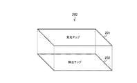
- FIG. 2 is a diagram illustrating an example of a stacked structure of the solid-state imaging device 200 according to the first embodiment of the present technology.
- the solid-state imaging device 200 includes a detection chip 202 and a light receiving chip 201 stacked on the detection chip 202. These chips are electrically connected through connection parts such as vias. In addition to the vias, the connection can be made by Cu—Cu bonding or bumps.
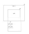
- FIG. 3 is an example of a plan view of the light receiving chip 201 according to the first embodiment of the present technology.
- the light receiving chip 201 is provided with a light receiving unit 220.
- a plurality of photodiodes 221 are arranged in a two-dimensional lattice pattern.
- the photodiode 221 generates photoelectric current by photoelectrically converting incident light.
- Each of these photodiodes 221 is assigned a pixel address composed of a row address and a column address, and is treated as a pixel.
- FIG. 4 is an example of a plan view of the detection chip 202 according to the first embodiment of the present technology.
- the detection chip 202 is provided with a signal processing circuit 230, a row drive circuit 251, a column drive circuit 252, an address holding unit 253, and an address event detection unit 260.
- the address event detection unit 260 detects, as an address event, that the absolute value of the amount of change in luminance exceeds a predetermined threshold value for each of the plurality of photodiodes 221 (pixels). Then, the address event detection unit 260 generates a detection signal indicating the detection result of the address event for each pixel and outputs the detection signal to the signal processing circuit 230 according to the enable signal.
- the enable signal is a signal indicating whether to enable the output of the detection signal for each of the plurality of pixels. If the enable signal is a value that enables the output, a detection signal is output from the corresponding pixel. On the other hand, when the enable signal is a value that invalidates the output, the detection signal is not output from the corresponding pixel.
- the row drive circuit 251 selects a row address and causes the address event detection unit 260 to output a detection signal corresponding to the row address.
- the column drive circuit 252 selects a column address and causes the address event detection unit 260 to output a detection signal corresponding to the column address.
- the address holding unit 253 holds a pixel address of a defective pixel in which an abnormality has occurred.
- the signal processing circuit 230 performs predetermined signal processing on the detection signal from the address event detection unit 260.
- the signal processing circuit 230 arranges the detection signals as pixel signals in a two-dimensional lattice pattern, and acquires image data. Then, the signal processing circuit 230 performs signal processing such as image recognition processing on the image data.
- the signal processing circuit 230 acquires the detection frequency of the address event for each pixel, and specifies the defective pixel based on the statistic of the detection frequency. Then, the signal processing circuit 230 holds the pixel address of the defective pixel in the address holding unit 253. Further, the signal processing circuit 230 generates an enable signal for each pixel and supplies it to the address event detection unit 260. Among these enable signals, the enable signal corresponding to the defective pixel is set to a value that invalidates the output.
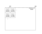
- FIG. 5 is an example of a plan view of the address event detection unit 260 according to the first embodiment of the present technology.
- this address event detection unit 260 a plurality of address event detection circuits 300 are arranged in a two-dimensional lattice pattern.
- Each address event detection circuit 300 is assigned a pixel address and is connected to a photodiode 221 having the same address.
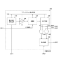
- FIG. 6 is a block diagram illustrating a configuration example of the address event detection circuit 300 according to the first embodiment of the present technology.
- the address event detection circuit 300 includes a current-voltage conversion circuit 310, a buffer 320, a subtracter 330, a quantizer 340, a transfer circuit 350, and N-type transistors 361 and 362.
- the current-voltage conversion circuit 310 converts the current signal from the corresponding photodiode 221 into a voltage signal.
- the current / voltage conversion circuit 310 supplies a voltage signal to the buffer 320.
- the buffer 320 outputs the input voltage signal to the subtracter 330.
- the buffer 320 can improve the driving force for driving the subsequent stage.
- the buffer 320 can ensure noise isolation associated with the subsequent switching operation.
- the subtractor 330 obtains the amount of change in the correction signal by subtraction.
- the subtracter 330 supplies the change amount as a differential signal to the quantizer 340.
- the quantizer 340 converts the analog differential signal into a digital detection signal (in other words, quantization) by comparing the differential signal with a predetermined threshold value.
- the quantizer 340 compares the differential signal with each of the upper threshold value and the lower threshold value, and supplies the comparison result to the transfer circuit 350 as a 2-bit detection signal.
- the quantizer 340 is an example of a comparator described in the claims.
- the N-type transistors 361 and 362 cut off the power supply of the current-voltage conversion circuit 310, the buffer 320, the subtractor 330, the quantizer 340, and the transfer circuit 350 according to the enable signal.
- these N-type transistors for example, MOS (Metal-Oxide-Semiconductor) transistors are used.
- N-type transistors 361 and 362 are connected in series between a power supply terminal and power supply line 363, and enable signals ENx and ENy from signal processing circuit 230 are input to their gates.
- the power supply line 363 is connected to the power supply terminals of the current-voltage conversion circuit 310, the buffer 320, the subtractor 330, and the quantizer 340.
- the N-type transistors 361 and 362 are examples of the transistors described in the claims.
- the enable signals ENx and ENy are signals for instructing whether or not to enable the output of the pixel whose pixel address is (x, y).
- both the enable signals ENx and ENy are set to a high level when enabled, and the low level is set to at least one when disabled.
- the transfer circuit 350 transfers the detection signal to the signal processing circuit 230 in accordance with the column drive signal from the column drive circuit 252.
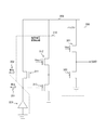
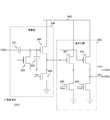
- FIG. 7 is a circuit diagram illustrating a configuration example of the current-voltage conversion circuit 310 and the buffer 320 according to the first embodiment of the present technology.
- the current-voltage conversion circuit 310 includes N-type transistors 311 and 313 and a P-type transistor 312. As these transistors, for example, MOS transistors are used.
- the source of the N-type transistor 311 is connected to the cathode of the photodiode 221, and the drain is connected to the power supply line 363.
- P-type transistor 312 and N-type transistor 313 are connected in series between power supply line 363 and the ground terminal.
- the connection point of the P-type transistor 312 and the N-type transistor 313 is connected to the gate of the N-type transistor 311 and the input terminal of the buffer 320.
- a predetermined bias voltage Vbais1 is applied to the gate of the P-type transistor 312.
- the drains of the N-type transistors 311 and 313 are connected to the power supply side, and such a circuit is called a source follower.
- the current signal from the photodiode 221 is converted into a voltage signal by the two source followers connected in a loop.
- the P-type transistor 312 supplies a constant current to the N-type transistor 313.
- the ground of the light receiving chip 201 and the ground of the detection chip 202 are separated from each other for interference countermeasures.
- the buffer 320 includes P-type transistors 321 and 322. As these transistors, for example, MOS transistors are used.
- P-type transistors 321 and 322 are connected in series between the power supply line 363 and the ground terminal.
- a predetermined bias voltage Vbsf is applied to the gate of the P-type transistor 321.
- the gate of the P-type transistor 322 is connected to the output terminal of the current-voltage conversion circuit 310.
- a correction signal is output to the subtractor 330 from the connection point of the P-type transistors 321 and 322.
- FIG. 8 is a circuit diagram illustrating a configuration example of the subtractor 330 and the quantizer 340 according to the first embodiment of the present technology.
- Subtractor 330 includes capacitors 331 and 332, P-type transistors 333 and 334, and N-type transistor 335.
- the P-type transistor 334 and the N-type transistor 335 are connected in series between the power supply line 363 and the ground terminal.
- the gate of the P-type transistor 334 serves as an input terminal
- the connection point between the P-type transistor 334 and the N-type transistor 335 serves as an output terminal
- the P-type transistor 334 and the N-type transistor 335 function as an inverter that inverts an input signal.
- Capacitor 332 is connected in parallel to the inverter.
- the P-type transistor 333 opens and closes a path connecting both ends of the capacitor 332 according to the row drive signal.
- Equation 5 represents the subtraction operation of the voltage signal, and the gain of the subtraction result is C1 / C2.
- the gain of the subtraction result is C1 / C2.
- C1 large and C2 small.
- C2 is too small, kTC noise increases and noise characteristics may be deteriorated. Therefore, the capacity reduction of C2 is limited to a range in which noise can be allowed.
- the capacitors C1 and C2 have an area limitation. Considering these, for example, C1 is set to a value of 20 to 200 femtofarads (fF), and C2 is set to a value of 1 to 20 femtofarads (fF).
- the quantizer 340 includes P-type transistors 341 and 342 and N-type transistors 343 and 344. As these transistors, for example, MOS transistors are used.
- P-type transistor 341 and N-type transistor 343 are connected in series between power supply line 363 and the ground terminal, and P-type transistor 342 and N-type transistor 344 are also connected in series between power supply line 363 and the ground terminal. Is done.
- the gates of the P-type transistors 341 and 342 are connected to the output terminal of the subtractor 330.
- a bias voltage Vbon indicating an upper limit threshold is applied to the gate of the N-type transistor 343, and a bias voltage Vboff indicating a lower limit threshold is applied to the gate of the N-type transistor 344.
- connection point between the P-type transistor 341 and the N-type transistor 343 is connected to the transfer circuit 350, and the voltage at this connection point is output as the on-event detection signal VCH.
- the connection point of the P-type transistor 342 and the N-type transistor 344 is also connected to the transfer circuit 350, and the voltage at this connection point is output as the off event detection signal VCL.
- the quantizer 340 outputs a high level on-event detection signal VCH when the differential signal exceeds the upper threshold, and detects a low level off event when the differential signal falls below the lower threshold.
- the signal VCL is output.
- the photodiode 221 is disposed on the light receiving chip 201 and the subsequent circuit is disposed on the detection chip 202
- the circuit disposed on each chip is not limited to this configuration.
- the photodiode 221 and the N-type transistors 311 and 313 can be arranged on the light receiving chip 201 and the others can be arranged on the detection chip 202.
- the photodiode 221 and the current-voltage conversion circuit 310 can be arranged on the light receiving chip 201, and the others can be arranged on the detection chip 202.
- the photodiode 221, the current-voltage conversion circuit 310, and the buffer 320 can be arranged on the light receiving chip 201, and the others can be arranged on the detection chip 202. Further, the photodiode 221, the current-voltage conversion circuit 310, the buffer 320, and the capacitor 331 can be arranged on the light receiving chip 201, and the others can be arranged on the detection chip 202. In addition, the photodiode 221, the current-voltage conversion circuit 310, the buffer 320, the subtractor 330, and the quantizer 340 can be arranged on the light receiving chip 201, and the others can be arranged on the detection chip 202.
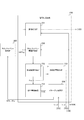
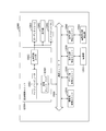
- FIG. 9 is a block diagram illustrating a configuration example of the signal processing circuit 230 according to the first embodiment of the present technology.
- the signal processing circuit 230 includes an image processing unit 231, an address event history recording unit 232, a detection frequency acquisition unit 233, a statistic acquisition unit 234, a defective pixel specification unit 235, and an enable setting unit 236.
- the mode signal MODE from the control unit 130 is input to the image processing unit 231 and the address event history recording unit 232.
- the mode signal MODE is a signal for designating either the test mode or the normal mode.
- the test mode is a mode in which the imaging apparatus 100 tests its own operation.
- the normal mode is a mode in which the imaging apparatus 100 performs a predetermined process such as image recognition without performing a test.
- the test mode is set by a user operation or execution of a predetermined application. It is desirable that the test mode is set in a situation where there is almost no change in luminance (for example, at the time of shipment or repair). In the test mode, it is desirable to block the solid-state image sensor 200 with a mechanical shutter or the like so that the luminance does not change.
- the image processing unit 231 executes predetermined processing such as image recognition in the normal mode, and outputs the processing result to the recording unit 120. On the other hand, in the test mode, the image processing unit 231 stops processing.
- the address event history recording unit 232 records the history of the detection signal DETxy for each pixel within a certain period in the test mode.
- the subscripts x and y indicate the row address and column address of the pixel.
- the detection frequency acquisition unit 233 refers to the history and acquires the detection frequency of the address event for each pixel.
- the detection frequency is calculated by, for example, dividing the number of address event detections within a certain period of each pixel by the unit time. The number of detections is counted without distinction between an on event and an off event. For example, when an on event is detected three times and an off event is detected twice within a certain period, the number of detections is five.
- the detection frequency acquisition unit 233 supplies the detection frequency Fxy for each pixel to the statistic acquisition unit 234 and the defective pixel specification unit 235.
- Statistic acquisition unit 234 acquires the statistic of detection frequency Fxy. For example, the statistic acquisition unit 234 calculates an average value AVE of the detection frequencies Fxy and supplies the average value AVE to the defective pixel specifying unit 235.
- the defective pixel specifying unit 235 specifies a defective pixel based on a statistic (such as an average value) of the detection frequency Fxy.
- the defective pixel specifying unit 235 determines, for each pixel, whether or not the detection frequency is a value deviating from the average value depending on whether or not the following expression is satisfied.
- Th is a predetermined real number.
- an address event is not detected if there is no change in luminance.
- the address event is erroneous even though the luminance has not changed due to the noise of the element in the pixel or the phenomenon that the charge to be held in the capacitor in the pixel is lost due to the leakage current. May be detected.
- the influence of the RTS (Random Telephone Signal) noise is particularly large as noise in the pixel.
- processing such as image recognition may be hindered by a meaningless detection signal, or a data band of an interface that transmits the detection signal may be compressed.
- the power consumption of the solid-state imaging device 200 may increase due to transmission or processing of a detection signal that is erroneously detected.
- a pixel that satisfies Equation 6 is a pixel whose false detection frequency deviates from the average value. Therefore, the defective pixel specifying unit 235 determines whether or not Expression 6 is satisfied for each pixel. Then, the defective pixel specifying unit 235 sets a pixel satisfying Expression 6 as a defective pixel, and causes the address holding unit 253 to hold the pixel address (x, y) of the defective pixel.
- the enable setting unit 236 generates and supplies an enable signal for each pixel.
- the enable setting unit 236 reads the pixel address of the defective pixel from the address holding unit 253 in the normal mode, sets the output of the defective pixel to be invalid by the enable signal, and sets the output to be valid for the remaining pixels by the enable signal. Then, the enable setting unit 236 supplies each of the generated enable signals to the address event detection unit 260.
- the enable signal setting unit 236 is an example of the invalidation setting unit described in the claims.
- the imaging apparatus 100 is configured not to perform a test during execution of processing performed in the normal mode, but is not limited to this configuration.
- the signal processing circuit 230 performs a test, and a configuration in which part or all of the processing (acquisition of detection frequency and statistics) performed in the test is performed in a circuit or device outside the signal processing circuit 230 You can also
- the statistic acquisition unit 234 acquires the average value of the detection frequencies as the statistic, but can also acquire a statistic other than the average value (such as variance and mode value).
- a statistic other than the average value such as variance and mode value.
- the statistic acquisition unit 234 calculates the variance for each pixel, and the defective pixel specifying unit 235 specifies a pixel whose variance is larger than a predetermined value as a defective pixel.
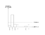
- FIG. 10 is a graph illustrating an example of the detection frequency of the address event for each pixel in the first embodiment of the present technology.
- the vertical axis indicates the detection frequency Fxy
- the horizontal axis indicates the pixel address.
- a dashed-dotted line shows the average value AVE.
- the detection frequency of the pixel at the pixel address (0, 0) is less than the average value AVE and does not satisfy Equation 6. For this reason, this pixel is determined to be a normal pixel.
- the detection frequency of the pixel at the pixel address (0, 1) greatly deviates from the average value AVE and satisfies Expression 6. For this reason, this pixel is determined to be a defective pixel.
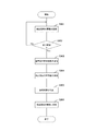
- FIG. 11 is a flowchart illustrating an example of the operation of the solid-state imaging device 200 according to the first embodiment of the present technology. This operation is started, for example, when the test mode is set.
- the address event history recording unit 232 records a history of detection signals for each pixel (step S901). Then, the address event history recording unit 232 determines whether or not the current time is the test end time (step S902). If it is not the end time (step S902: No), the address event history recording unit 232 repeatedly executes step S901 and subsequent steps.
- step S902 when it is the end time (step S902: Yes), the detection frequency acquisition unit 233 acquires the detection frequency of the address event for each pixel (step S903), and the statistic acquisition unit 234 calculates the average value of the detection frequencies. Is calculated (step S904).
- the defective pixel specifying unit 235 specifies a defective pixel using Equation 6 (step S905), and the enable setting unit 236 sets the value of the enable signal of the defective pixel to a value that invalidates the output (step S906). . After step S906, the solid-state imaging device 200 ends the operation for the test.
- the solid-state imaging device 200 acquires the detection frequency for each pixel, and identifies the defective pixel in which an abnormality has occurred based on the statistical amount. A test can be easily performed without using a light source.
- Second Embodiment> In the first embodiment described above, the defective pixel is disabled by shutting off the power supply. However, when the power is turned off, the output of both the on event and the off event is invalidated, and it is impossible to invalidate only one of the on event detection and the off event detection.
- the address event detection circuit 300 according to the second embodiment is different from the first embodiment in that the on event detection signal and the off event detection signal are individually blocked.
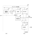
- FIG. 12 is a block diagram illustrating a configuration example of the address event detection circuit 300 according to the second embodiment of the present technology.
- the address event detection circuit 300 of the second embodiment is different from that of the first embodiment in that it further includes AND (logical product) gates 364 and 365.
- a 1-bit enable signal ENoff from the signal processing circuit 230 is input to the AND gate 364, and a 1-bit enable signal ENon from the signal processing circuit 230 is input to the AND gate 365.
- these enable signals are set to a high level when enabled, and set to a low level when disabled.
- the AND gate 364 outputs a logical product of the enable signal ENoff and the off event detection signal VCL from the quantizer 340 to the transfer circuit.
- the enable signal ENoff is at a low level, the output of the off event detection signal VCL is blocked by the AND gate 364.
- the AND gate 364 is an example of a second logic gate described in the claims.
- the AND gate 365 outputs a logical product of the enable signal ENon and the on-event detection signal VCH from the quantizer 340 to the transfer circuit. When the enable signal ENon is at a low level, the output of the on event detection signal VCH is blocked by the AND gate 365.
- the AND gate 365 is an example of a first logic gate described in the claims.
- the detection frequency acquisition unit 233 acquires the on-event detection frequency Fon and the off-event detection frequency Foff individually for each pixel.
- the statistic acquisition unit 234 also individually acquires the statistic of the on-event detection frequency (such as the average value AVEon) and the statistic of the off-event detection frequency (such as the average value AVEoff). Then, the defective pixel specifying unit 235 determines whether or not the following expression is satisfied for each pixel. Fon> AVEon + Th (7) Foff> AVEoff + Th (8)
- Pixels that do not satisfy one of Equations 7 and 8 are treated as defective pixels.
- the enable setting unit 236 sets a low level to the enable signal ENon of the defective pixel that does not satisfy Expression 7, and sets a low level to the enable signal ENoff of the defective pixel that does not satisfy Expression 8. Thereby, when there is an abnormality in the detection of only one of the on event and the off event, the output of only one of them can be invalidated.
- the AND gates 364 and 365 individually block the output of the on event detection signal and the off event detection signal, so that only one detection is abnormal. If there is, only that output can be disabled.
- the signal processing circuit 230 reads the pixel address of the defective pixel from the address holding unit 253, generates an enable signal, and supplies the enable signal to each pixel.
- the wiring distance of the signal line for transmitting the enable signal becomes long, and there is a possibility that transmission of the enable signal may be delayed.
- the solid-state imaging device 200 according to the third embodiment is different from the second embodiment in that an enable signal is held for each pixel.
- FIG. 13 is an example of a plan view of the detection chip 202 according to the third embodiment of the present technology.
- the detection chip 202 according to the third embodiment is different from the second embodiment in that the address holding unit 253 is not disposed.
- FIG. 14 is a block diagram illustrating a configuration example of the address event detection circuit 300 according to the third embodiment of the present technology.
- the address event detection circuit 300 according to the third embodiment is different from the second embodiment in that an enable signal holding unit 366 is further provided.
- the enable signal holding unit 366 holds the enable signals ENon and ENoff from the signal processing circuit 230.
- the enable signal holding unit 366 is realized by, for example, a latch circuit or a flip-flop.
- the enable signal holding unit 366 supplies the hold value to the AND gates 364 and 365, respectively.
- the solid-state imaging device 200 can also shut off the power supply by an enable signal, as in the first embodiment.
- N-type transistors 361 and 362 are arranged instead of AND gates 364 and 365.
- the address event detection circuit 300 since the address event detection circuit 300 holds the enable signal of the corresponding pixel, as compared with the case where the enable signal is transmitted from the signal processing circuit 230, The transmission delay of the enable signal can be suppressed.
- the technology according to the present disclosure can be applied to various products.
- the technology according to the present disclosure is realized as a device that is mounted on any type of mobile body such as an automobile, an electric vehicle, a hybrid electric vehicle, a motorcycle, a bicycle, personal mobility, an airplane, a drone, a ship, and a robot. May be.
- FIG. 15 is a block diagram illustrating a schematic configuration example of a vehicle control system that is an example of a mobile control system to which the technology according to the present disclosure can be applied.
- the vehicle control system 12000 includes a plurality of electronic control units connected via a communication network 12001.
- the vehicle control system 12000 includes a drive system control unit 12010, a body system control unit 12020, a vehicle exterior information detection unit 12030, a vehicle interior information detection unit 12040, and an integrated control unit 12050.
- a microcomputer 12051, a sound image output unit 12052, and an in-vehicle network I / F (interface) 12053 are illustrated as a functional configuration of the integrated control unit 12050.
- the drive system control unit 12010 controls the operation of the device related to the drive system of the vehicle according to various programs.
- the drive system control unit 12010 includes a driving force generator for generating a driving force of a vehicle such as an internal combustion engine or a driving motor, a driving force transmission mechanism for transmitting the driving force to wheels, and a steering angle of the vehicle. It functions as a control device such as a steering mechanism that adjusts and a braking device that generates a braking force of the vehicle.
- the body system control unit 12020 controls the operation of various devices mounted on the vehicle body according to various programs.
- the body system control unit 12020 functions as a keyless entry system, a smart key system, a power window device, or a control device for various lamps such as a headlamp, a back lamp, a brake lamp, a blinker, or a fog lamp.
- the body control unit 12020 can be input with radio waves transmitted from a portable device that substitutes for a key or signals from various switches.
- the body system control unit 12020 receives input of these radio waves or signals, and controls a door lock device, a power window device, a lamp, and the like of the vehicle.
- the imaging unit 12031 is an optical sensor that receives light and outputs an electrical signal corresponding to the amount of received light.
- the imaging unit 12031 can output an electrical signal as an image, or can output it as distance measurement information. Further, the light received by the imaging unit 12031 may be visible light or invisible light such as infrared rays.
- the vehicle interior information detection unit 12040 detects vehicle interior information.
- a driver state detection unit 12041 that detects a driver's state is connected to the in-vehicle information detection unit 12040.
- the driver state detection unit 12041 includes, for example, a camera that images the driver, and the vehicle interior information detection unit 12040 determines the degree of fatigue or concentration of the driver based on the detection information input from the driver state detection unit 12041. It may be calculated or it may be determined whether the driver is asleep.
- the microcomputer 12051 calculates a control target value of the driving force generator, the steering mechanism, or the braking device based on the information inside / outside the vehicle acquired by the vehicle outside information detection unit 12030 or the vehicle interior information detection unit 12040, and the drive system control unit A control command can be output to 12010.
- the microcomputer 12051 realizes ADAS (Advanced Driver Assistance System) functions including vehicle collision avoidance or impact mitigation, tracking based on inter-vehicle distance, vehicle speed maintenance traveling, vehicle collision warning, or vehicle lane departure warning. It is possible to perform cooperative control for the purpose.
- ADAS Advanced Driver Assistance System
- the microcomputer 12051 controls the driving force generator, the steering mechanism, the braking device, and the like based on the information around the vehicle acquired by the vehicle exterior information detection unit 12030 or the vehicle interior information detection unit 12040. It is possible to perform cooperative control for the purpose of automatic driving that autonomously travels without depending on the operation.
- the microcomputer 12051 can output a control command to the body system control unit 12020 based on information outside the vehicle acquired by the vehicle outside information detection unit 12030.
- the microcomputer 12051 controls the headlamp according to the position of the preceding vehicle or the oncoming vehicle detected by the outside information detection unit 12030, and performs cooperative control for the purpose of anti-glare, such as switching from a high beam to a low beam. It can be carried out.
- the sound image output unit 12052 transmits an output signal of at least one of sound and image to an output device capable of visually or audibly notifying information to a vehicle occupant or the outside of the vehicle.
- an audio speaker 12061, a display unit 12062, and an instrument panel 12063 are illustrated as output devices.
- the display unit 12062 may include at least one of an on-board display and a head-up display, for example.
- FIG. 16 is a diagram illustrating an example of an installation position of the imaging unit 12031.
- the imaging unit 12031 includes imaging units 12101, 12102, 12103, 12104, and 12105.
- the imaging units 12101, 12102, 12103, 12104, and 12105 are provided, for example, at positions such as a front nose, a side mirror, a rear bumper, a back door, and an upper part of a windshield in the vehicle interior of the vehicle 12100.
- the imaging unit 12101 provided in the front nose and the imaging unit 12105 provided in the upper part of the windshield in the vehicle interior mainly acquire an image in front of the vehicle 12100.
- the imaging units 12102 and 12103 provided in the side mirror mainly acquire an image of the side of the vehicle 12100.
- the imaging unit 12104 provided in the rear bumper or the back door mainly acquires an image behind the vehicle 12100.
- the imaging unit 12105 provided on the upper part of the windshield in the passenger compartment is mainly used for detecting a preceding vehicle or a pedestrian, an obstacle, a traffic light, a traffic sign, a lane, or the like.
- FIG. 16 shows an example of the shooting range of the imaging units 12101 to 12104.
- the imaging range 12111 indicates the imaging range of the imaging unit 12101 provided in the front nose
- the imaging ranges 12112 and 12113 indicate the imaging ranges of the imaging units 12102 and 12103 provided in the side mirrors, respectively
- the imaging range 12114 The imaging range of the imaging part 12104 provided in the rear bumper or the back door is shown. For example, by superimposing the image data captured by the imaging units 12101 to 12104, an overhead image when the vehicle 12100 is viewed from above is obtained.
- At least one of the imaging units 12101 to 12104 may have a function of acquiring distance information.
- at least one of the imaging units 12101 to 12104 may be a stereo camera including a plurality of imaging elements, or may be an imaging element having pixels for phase difference detection.
- the microcomputer 12051 based on the distance information obtained from the imaging units 12101 to 12104, the distance to each three-dimensional object in the imaging range 12111 to 12114 and the temporal change in this distance (relative speed with respect to the vehicle 12100).
- a predetermined speed for example, 0 km / h or more
- the microcomputer 12051 can set an inter-vehicle distance to be secured in advance before the preceding vehicle, and can perform automatic brake control (including follow-up stop control), automatic acceleration control (including follow-up start control), and the like.
- automatic brake control including follow-up stop control
- automatic acceleration control including follow-up start control
- cooperative control for the purpose of autonomous driving or the like autonomously traveling without depending on the operation of the driver can be performed.
- the microcomputer 12051 converts the three-dimensional object data regarding the three-dimensional object to other three-dimensional objects such as a two-wheeled vehicle, a normal vehicle, a large vehicle, a pedestrian, and a power pole based on the distance information obtained from the imaging units 12101 to 12104. It can be classified and extracted and used for automatic avoidance of obstacles. For example, the microcomputer 12051 identifies obstacles around the vehicle 12100 as obstacles that are visible to the driver of the vehicle 12100 and obstacles that are difficult to see. The microcomputer 12051 determines the collision risk indicating the risk of collision with each obstacle, and when the collision risk is equal to or higher than the set value and there is a possibility of collision, the microcomputer 12051 is connected via the audio speaker 12061 or the display unit 12062. By outputting an alarm to the driver and performing forced deceleration or avoidance steering via the drive system control unit 12010, driving assistance for collision avoidance can be performed.
- the microcomputer 12051 converts the three-dimensional object data regarding the three-dimensional object to other three-dimensional objects such
- At least one of the imaging units 12101 to 12104 may be an infrared camera that detects infrared rays.
- the microcomputer 12051 can recognize a pedestrian by determining whether a pedestrian is present in the captured images of the imaging units 12101 to 12104. Such pedestrian recognition is, for example, whether or not the user is a pedestrian by performing a pattern matching process on a sequence of feature points indicating the outline of an object and a procedure for extracting feature points in the captured images of the imaging units 12101 to 12104 as infrared cameras. It is carried out by the procedure for determining.
- the audio image output unit 12052 When the microcomputer 12051 determines that there is a pedestrian in the captured images of the imaging units 12101 to 12104 and recognizes the pedestrian, the audio image output unit 12052 has a rectangular contour line for emphasizing the recognized pedestrian.
- the display unit 12062 is controlled so as to be superimposed and displayed.
- voice image output part 12052 may control the display part 12062 so that the icon etc. which show a pedestrian may be displayed on a desired position.
- the technology according to the present disclosure can be applied to the imaging unit 12031 among the configurations described above.
- the imaging apparatus 100 in FIG. 1 can be applied to the imaging unit 12031.
- the processing procedure described in the above embodiment may be regarded as a method having a series of these procedures, and a program for causing a computer to execute these series of procedures or a recording medium storing the program. You may catch it.
- a recording medium for example, a CD (Compact Disc), an MD (MiniDisc), a DVD (Digital Versatile Disc), a memory card, a Blu-ray disc (Blu-ray (registered trademark) Disc), or the like can be used.
- this technique can also take the following structures.
- an address event detection unit that detects that the absolute value of the amount of change in luminance exceeds a predetermined threshold for each of a plurality of pixels as an address event and outputs a detection signal indicating the detection result;
- a detection frequency acquisition unit that acquires the detection frequency of the address event for each of the plurality of pixels;
- a solid-state imaging device comprising: a defective pixel specifying unit that specifies a defective pixel having an abnormality among the plurality of pixels based on a statistic of the detection frequency.
- the address event detection unit includes an address event detection circuit for each of the plurality of pixels.
- the address event detection circuit includes: A current-voltage conversion circuit that converts a photocurrent generated by photoelectric conversion into a voltage signal; A subtractor that outputs a change amount of the voltage signal as a differential signal by subtraction;
- the solid-state imaging device according to (2) further comprising: a quantizer that generates a signal indicating a comparison result between the differential signal and the threshold value and outputs the signal as the detection signal.
- the address event detection circuit further includes a transistor that shuts off a power source of the current-voltage conversion circuit, the subtracter, and the quantizer according to the setting of the invalidation setting unit. .
- an address event detector that detects that the absolute value of the amount of change in luminance exceeds a predetermined threshold for each of the plurality of pixels as an address event and outputs a detection signal indicating the detection result;
- a detection frequency acquisition unit that acquires the detection frequency of the address event for each of the plurality of pixels;
- a defective pixel specifying unit that specifies a defective pixel in which an abnormality has occurred among the plurality of pixels based on the statistic of the detection frequency;
- An imaging apparatus comprising: an image processing unit that processes image data including the detection signal.
Landscapes
- Engineering & Computer Science (AREA)
- Multimedia (AREA)
- Signal Processing (AREA)
- Transforming Light Signals Into Electric Signals (AREA)
- Studio Devices (AREA)
Abstract
アドレスイベントを検出する固体撮像素子において、欠陥画素を容易に特定する。 アドレスイベント検出部は、複数の画素のそれぞれについて輝度の変化量の絶対値が所定の閾値を超えた旨をアドレスイベントとして検出して当該検出結果を示す検出信号を出力する。検出頻度取得部は、複数の画素のそれぞれについて前記アドレスイベントの検出頻度を取得する。欠陥画素特定部は、検出頻度の統計量に基づいて前記複数の画素のうち異常の生じた欠陥画素を特定する。
Description
本技術は固体撮像素子、撮像装置、および、固体撮像素子の制御方法に関する。詳しくは、入射光の光量を閾値と比較する固体撮像素子、撮像装置、および、固体撮像素子の制御方法に関する。
従来より、垂直同期信号などの同期信号に同期して画像データ(フレーム)を撮像する同期型の固体撮像素子が、撮像装置などにおいて用いられている。この一般的な同期型の固体撮像素子では、同期信号の周期(例えば、1/60秒)ごとにしか画像データを取得することができないため、自動運転やウェアラブルデバイスのユーザインターフェースなどに関する分野において、より高速な処理が要求された場合に対応することが困難になる。そこで、画素アドレスごとに、輝度の変化量が閾値を超えた旨をアドレスイベントとしてリアルタイムに検出するアドレスイベント検出回路を設けた非同期型の固体撮像素子が提案されている(例えば、特許文献1参照。)。この固体撮像素子の動作をテストする方法としては、例えば、パルス光を照射する変調光源を載置し、そのパルス光の照射時の検出結果を分析するテスト方法が挙げられる。
上述の非同期型の固体撮像素子では、パルス光の照射時の検出結果を分析することにより、異常のある欠陥画素を特定することができる。しかしながら、このテスト方法では、変調光源や、その変調光源を制御する装置が必要となるため、システムの規模が大きくなり、テストが困難となるおそれがある。
本技術はこのような状況に鑑みて生み出されたものであり、アドレスイベントを検出する固体撮像素子において、欠陥画素を容易に特定することを目的とする。
本技術は、上述の問題点を解消するためになされたものであり、その第1の側面は、複数の画素のそれぞれについて輝度の変化量の絶対値が所定の閾値を超えた旨をアドレスイベントとして検出して当該検出結果を示す検出信号を出力するアドレスイベント検出部と、上記複数の画素のそれぞれについて上記アドレスイベントの検出頻度を取得する検出頻度取得部と、上記検出頻度の統計量に基づいて上記複数の画素のうち異常の生じた欠陥画素を特定する欠陥画素特定部とを具備する固体撮像素子、および、その制御方法である。これにより、検出頻度の統計量に基づいて欠陥画素が特定されるという作用をもたらす。
また、この第1の側面において、上記欠陥画素に対応する上記検出信号の出力を無効に設定する無効化設定部をさらに具備してもよい。これにより、欠陥画素の出力が無効になるという作用をもたらす。
また、この第1の側面において、上記アドレスイベント検出部は、上記複数の画素のそれぞれについてアドレスイベント検出回路を備え、上記アドレスイベント検出回路は、光電変換により生成された光電流を電圧信号に変換する電流電圧変換回路と、減算により上記電圧信号の変化量を微分信号として出力する減算器と、上記微分信号と上記閾値との比較結果を示す信号を生成して上記検出信号として出力する量子化器とを備えてもよい。これにより、光電流から検出信号が生成されるという作用をもたらす。
また、この第1の側面において、上記アドレスイベント検出回路は、上記無効化設定部の設定に従って上記電流電圧変換回路、上記減算器および上記量子化器の電源を遮断するトランジスタをさらに備えてもよい。これにより、電流電圧変換回路、減算器および量子化器の電源が遮断されるという作用をもたらす。
また、この第1の側面において、上記アドレスイベントはオンイベントおよびオフイベントを含み、上記検出信号は、上記オフイベントの検出信号と上記オンイベントの検出信号とを含み、上記アドレスイベント検出回路は、上記イネーブル信号に従って上記量子化器からの上記オンイベントの検出信号を遮断する第1の論理ゲートと、上記イネーブル信号に従って上記量子化器からの上記オフイベントの検出信号を遮断する第2の論理ゲートとを備えてもよい。これにより、オンイベントの検出信号とオフイベントの検出信号とが個別に遮断されるという作用をもたらす。
また、この第1の側面において、上記欠陥画素のアドレスを保持するアドレス保持部をさらに具備し、前記設定部は、前記アドレス保持部から前記アドレスを読み出して当該アドレスに対応する前記検出信号の出力を無効に設定してもよい。これにより、保持されたアドレスに対応する検出信号の出力が無効に設定されるという作用をもたらす。
また、この第1の側面において、上記アドレスイベント検出回路は、当該アドレスイベント検出回路に対応する上記検出信号の出力を有効にするか否かを示すイネーブル信号を保持するイネーブル信号保持部をさらに備え、上記設定部は、上記イネーブル信号により上記検出信号の出力を無効に設定してもよい。これにより、画素ごとにイネーブル信号が保持されるという作用をもたらす。
また、この第1の側面において、上記統計量は、平均値であり、上記欠陥画素特定部は、上記検出頻度が上記平均値から外れた画素を上記欠陥画素として特定してもよい。これにより、検出頻度が上記平均値から外れた画素が欠陥画素として特定されるという作用をもたらす。
また、本技術の第2の側面は、複数の画素のそれぞれについて輝度の変化量の絶対値が所定の閾値を超えた旨をアドレスイベントとして検出して当該検出結果を示す検出信号を出力するアドレスイベント検出部と、上記複数の画素のそれぞれについて上記アドレスイベントの検出頻度を取得する検出頻度取得部と、上記検出頻度の統計量に基づいて上記複数の画素のうち異常の生じた欠陥画素を特定する欠陥画素特定部と、上記検出信号からなる画像データを処理する画像処理部とを具備する撮像装置である。検出頻度の統計量に基づいて欠陥画素が特定され、画像データが処理されるという作用をもたらす。
本技術によれば、アドレスイベントを検出する固体撮像素子において、欠陥画素を容易に特定することができるという優れた効果を奏し得る。なお、ここに記載された効果は必ずしも限定されるものではなく、本開示中に記載されたいずれかの効果であってもよい。
以下、本技術を実施するための形態(以下、実施の形態と称する)について説明する。説明は以下の順序により行う。
1.第1の実施の形態(統計量に基づいて欠陥画素を特定する例)
2.第2の実施の形態(統計量に基づいて欠陥画素を特定し、出力を遮断する例)
3.第3の実施の形態(統計量に基づいて欠陥画素を特定し、画素毎にイネーブル信号を保持する例)
4.移動体への応用例
1.第1の実施の形態(統計量に基づいて欠陥画素を特定する例)
2.第2の実施の形態(統計量に基づいて欠陥画素を特定し、出力を遮断する例)
3.第3の実施の形態(統計量に基づいて欠陥画素を特定し、画素毎にイネーブル信号を保持する例)
4.移動体への応用例
<1.第1の実施の形態>
[撮像装置の構成例]
図1は、本技術の第1の実施の形態における撮像装置100の一構成例を示すブロック図である。この撮像装置100は、撮像レンズ110、固体撮像素子200、記録部120および制御部130を備える。撮像装置100としては、ウェアラブルデバイスに搭載されるカメラや、車載カメラなどが想定される。
[撮像装置の構成例]
図1は、本技術の第1の実施の形態における撮像装置100の一構成例を示すブロック図である。この撮像装置100は、撮像レンズ110、固体撮像素子200、記録部120および制御部130を備える。撮像装置100としては、ウェアラブルデバイスに搭載されるカメラや、車載カメラなどが想定される。
撮像レンズ110は、入射光を集光して固体撮像素子200に導くものである。
固体撮像素子200は、複数の画素のそれぞれについて、輝度の変化量の絶対値が閾値を超えた旨をアドレスイベントとして検出するものである。このアドレスイベントは、例えば、輝度の上昇量が上限閾値を超えた旨を示すオンイベントと、輝度の低下量が上限閾値未満の下限閾値を下回った旨を示すオフイベントとを含む。そして、固体撮像素子200は、アドレスイベントの検出結果を示す検出信号を画素毎に生成する。それぞれの検出信号は、オンイベントの有無を示すオンイベント検出信号VCHと、オフイベントの有無を示すオフイベント検出信号VCLとを含む。なお、固体撮像素子200は、オンイベントおよびオフイベントの両方の有無を検出しているが、一方のみを検出することもできる。
固体撮像素子200は、検出信号からなる画像データに対し、画像認識処理などの所定の信号処理を実行し、その処理後のデータを記録部120に信号線209を介して出力する。
記録部120は、固体撮像素子200からのデータを記録するものである。制御部130は、固体撮像素子200を制御して画像データを撮像させるものである。
[固体撮像素子の構成例]
図2は、本技術の第1の実施の形態における固体撮像素子200の積層構造の一例を示す図である。この固体撮像素子200は、検出チップ202と、その検出チップ202に積層された受光チップ201とを備える。これらのチップは、ビアなどの接続部を介して電気的に接続される。なお、ビアの他、Cu-Cu接合やバンプにより接続することもできる。
図2は、本技術の第1の実施の形態における固体撮像素子200の積層構造の一例を示す図である。この固体撮像素子200は、検出チップ202と、その検出チップ202に積層された受光チップ201とを備える。これらのチップは、ビアなどの接続部を介して電気的に接続される。なお、ビアの他、Cu-Cu接合やバンプにより接続することもできる。
図3は、本技術の第1の実施の形態における受光チップ201の平面図の一例である。受光チップ201には、受光部220が設けられる。受光部220には、二次元格子状に複数のフォトダイオード221が配列される。フォトダイオード221は、入射光を光電変換して光電流を生成するものである。これらのフォトダイオード221のそれぞれには、行アドレスおよび列アドレスからなる画素アドレスが割り当てられ、画素として扱われる。
図4は、本技術の第1の実施の形態における検出チップ202の平面図の一例である。この検出チップ202には、信号処理回路230、行駆動回路251、列駆動回路252、アドレス保持部253およびアドレスイベント検出部260が設けられる。
アドレスイベント検出部260は、複数のフォトダイオード221(画素)のそれぞれについて輝度の変化量の絶対値が所定の閾値を超えた旨をアドレスイベントとして検出するものである。そして、アドレスイベント検出部260は、アドレスイベントの検出結果を示す検出信号を画素毎に生成し、イネーブル信号に従って信号処理回路230に出力する。
ここで、イネーブル信号は、複数の画素のそれぞれについて検出信号の出力を有効にするか否かを示す信号である。イネーブル信号が出力を有効にする値である場合には、対応する画素から検出信号が出力される。一方、イネーブル信号が出力を無効にする値である場合には、対応する画素から検出信号は出力されない。
行駆動回路251は、行アドレスを選択して、その行アドレスに対応する検出信号をアドレスイベント検出部260に出力させるものである。
列駆動回路252は、列アドレスを選択して、その列アドレスに対応する検出信号をアドレスイベント検出部260に出力させるものである。
アドレス保持部253は、異常が生じた欠陥画素の画素アドレスを保持するものである。
信号処理回路230は、アドレスイベント検出部260からの検出信号に対して所定の信号処理を実行するものである。この信号処理回路230は、検出信号を画素信号として二次元格子状に配列し、画像データを取得する。そして、信号処理回路230は、その画像データに対して画像認識処理などの信号処理を実行する。
また、信号処理回路230は、画素ごとにアドレスイベントの検出頻度を取得し、その検出頻度の統計量に基づいて欠陥画素を特定する。そして、信号処理回路230は、その欠陥画素の画素アドレスをアドレス保持部253に保持しておく。また、信号処理回路230は、画素毎にイネーブル信号を生成してアドレスイベント検出部260に供給する。これらのイネーブル信号のうち、欠陥画素に対応するイネーブル信号は、出力を無効にする値に設定される。
図5は、本技術の第1の実施の形態におけるアドレスイベント検出部260の平面図の一例である。このアドレスイベント検出部260には、二次元格子状に複数のアドレスイベント検出回路300が配列される。アドレスイベント検出回路300のそれぞれには画素アドレスが割り当てられ、同一アドレスのフォトダイオード221と接続される。
アドレスイベント検出回路300は、対応するフォトダイオード221からの光電流に応じた電圧信号を量子化し、イネーブル信号に従って検出信号として出力するものである。
[アドレスイベント検出回路の構成例]
図6は、本技術の第1の実施の形態におけるアドレスイベント検出回路300の一構成例を示すブロック図である。このアドレスイベント検出回路300は、電流電圧変換回路310と、バッファ320と、減算器330と、量子化器340と、転送回路350と、N型トランジスタ361および362とを備える。
図6は、本技術の第1の実施の形態におけるアドレスイベント検出回路300の一構成例を示すブロック図である。このアドレスイベント検出回路300は、電流電圧変換回路310と、バッファ320と、減算器330と、量子化器340と、転送回路350と、N型トランジスタ361および362とを備える。
電流電圧変換回路310は、対応するフォトダイオード221からの電流信号を電圧信号に変換するものである。この電流電圧変換回路310は、電圧信号をバッファ320に供給する。
バッファ320は、入力された電圧信号を減算器330に出力するものである。このバッファ320により、後段を駆動する駆動力を向上させることができる。また、バッファ320により、後段のスイッチング動作に伴うノイズのアイソレーションを確保することができる。
減算器330は、減算により、補正信号の変化量を求めるものである。この減算器330は、変化量を微分信号として量子化器340に供給する。
量子化器340は、微分信号と所定の閾値との比較により、アナログの微分信号をデジタルの検出信号に変換(言い換えれば、量子化)するものである。この量子化器340は、微分信号と上限閾値および下限閾値のそれぞれとを比較し、それらの比較結果を2ビットの検出信号として転送回路350に供給する。なお、量子化器340は、特許請求の範囲に記載の比較器の一例である。
N型トランジスタ361および362は、イネーブル信号に従って電流電圧変換回路310、バッファ320、減算器330、量子化器340および転送回路350の電源を遮断するものである。これらのN型トランジスタとして、例えば、MOS(Metal-Oxide-Semiconductor)トランジスタが用いられる。N型トランジスタ361および362は、電源端子と、電源線363との間に直列に接続され、それらのゲートには、信号処理回路230からのイネーブル信号ENxおよびENyが入力される。この電源線363は、電流電圧変換回路310、バッファ320、減算器330、量子化器340のそれぞれの電源端子に接続される。なお、N型トランジスタ361および362は、特許請求の範囲に記載のトランジスタの一例である。
ここで、イネーブル信号ENxおよびENyは、画素アドレスが(x、y)の画素の出力を有効にするか否かを指示する信号である。例えば、有効にする場合にイネーブル信号ENxおよびENyの両方にハイレベルが設定され、無効にする場合に、少なくとも一方にローレベルが設定される。
転送回路350は、列駆動回路252からの列駆動信号に従って、検出信号を信号処理回路230に転送するものである。
[電流電圧変換回路およびバッファの構成例]
図7は、本技術の第1の実施の形態における電流電圧変換回路310およびバッファ320の一構成例を示す回路図である。
図7は、本技術の第1の実施の形態における電流電圧変換回路310およびバッファ320の一構成例を示す回路図である。
電流電圧変換回路310は、N型トランジスタ311および313とP型トランジスタ312とを備える。これらのトランジスタとして、例えば、MOSトランジスタが用いられる。
N型トランジスタ311のソースはフォトダイオード221のカソードに接続され、ドレインは電源線363に接続される。P型トランジスタ312およびN型トランジスタ313は、電源線363と接地端子との間において、直列に接続される。また、P型トランジスタ312およびN型トランジスタ313の接続点は、N型トランジスタ311のゲートとバッファ320の入力端子とに接続される。また、P型トランジスタ312のゲートには、所定のバイアス電圧Vbais1が印加される。
N型トランジスタ311および313のドレインは電源側に接続されており、このような回路はソースフォロワと呼ばれる。これらのループ状に接続された2つのソースフォロワにより、フォトダイオード221からの電流信号は電圧信号に変換される。また、P型トランジスタ312は、一定の電流をN型トランジスタ313に供給する。
また、受光チップ201のグランドと検出チップ202のグランドとは、干渉対策のために互いに分離されている。
バッファ320は、P型トランジスタ321および322を備える。これらのトランジスタとして、例えば、MOSトランジスタが用いられる。
P型トランジスタ321および322は、電源線363と接地端子との間において直列に接続される。また、P型トランジスタ321のゲートには所定のバイアス電圧Vbsfが印加される。P型トランジスタ322のゲートは、電流電圧変換回路310の出力端子に接続される。P型トランジスタ321および322の接続点からは、補正信号が減算器330へ出力される。
[減算器および量子化器の構成例]
図8は、本技術の第1の実施の形態における減算器330および量子化器340の一構成例を示す回路図である。減算器330は、コンデンサ331および332と、P型トランジスタ333および334と、N型トランジスタ335とを備える。
図8は、本技術の第1の実施の形態における減算器330および量子化器340の一構成例を示す回路図である。減算器330は、コンデンサ331および332と、P型トランジスタ333および334と、N型トランジスタ335とを備える。
P型トランジスタ334およびN型トランジスタ335は、電源線363と接地端子との間に直列に接続される。P型トランジスタ334のゲートを入力端子、P型トランジスタ334およびN型トランジスタ335の接続点を出力端子として、P型トランジスタ334およびN型トランジスタ335は入力信号を反転するインバータとして機能する。
コンデンサ331の一端は、バッファ320の出力端子に接続され、他端は、インバータの入力端子(すなわち、P型トランジスタ334のゲート)に接続される。コンデンサ332は、インバータに並列に接続される。P型トランジスタ333は、コンデンサ332の両端を接続する経路を行駆動信号に従って開閉するものである。
P型トランジスタ333をオンした際にコンデンサ331のバッファ320側に電圧信号Vinitが入力され、その逆側は仮想接地端子となる。この仮想接地端子の電位を便宜上、ゼロとする。このとき、コンデンサ331に蓄積されている電位Qinitは、コンデンサ331の容量をC1とすると、次の式により表される。一方、コンデンサ332の両端は、短絡されているため、その蓄積電荷はゼロとなる。
Qinit=C1×Vinit ・・・式1
Qinit=C1×Vinit ・・・式1
次に、P型トランジスタ333がオフされて、コンデンサ331のバッファ320側の電圧が変化してVafterになった場合を考えると、コンデンサ331に蓄積される電荷Qafterは、次の式により表される。
Qafter=C1×Vafter ・・・式2
Qafter=C1×Vafter ・・・式2
一方、コンデンサ332に蓄積される電荷Q2は、出力電圧をVoutとすると、次の式により表される。
Q2=-C2×Vout ・・・式3
Q2=-C2×Vout ・・・式3
このとき、コンデンサ331および332の総電荷量は変化しないため、次の式が成立する。
Qinit=Qafter+Q2 ・・・式4
Qinit=Qafter+Q2 ・・・式4
式4に式1乃至式3を代入して変形すると、次の式が得られる。
Vout=-(C1/C2)×(Vafter-Vinit) ・・・式5
Vout=-(C1/C2)×(Vafter-Vinit) ・・・式5
式5は、電圧信号の減算動作を表し、減算結果の利得はC1/C2となる。通常、利得を最大化することが望まれるため、C1を大きく、C2を小さく設計することが好ましい。一方、C2が小さすぎると、kTCノイズが増大し、ノイズ特性が悪化するおそれがあるため、C2の容量削減は、ノイズを許容することができる範囲に制限される。また、画素ごとに減算器330を含むアドレスイベント検出回路300が搭載されるため、容量C1やC2には、面積上の制約がある。これらを考慮して、例えば、C1は、20乃至200フェムトファラッド(fF)の値に設定され、C2は、1乃至20フェムトファラッド(fF)の値に設定される。
量子化器340は、P型トランジスタ341および342とN型トランジスタ343および344とを備える。これらのトランジスタとして、例えば、MOSトランジスタが用いられる。
P型トランジスタ341およびN型トランジスタ343は、電源線363と接地端子との間において直列に接続され、P型トランジスタ342およびN型トランジスタ344も、電源線363と接地端子との間において直列に接続される。また、P型トランジスタ341および342のゲートは、減算器330の出力端子に接続される。N型トランジスタ343のゲートには上限閾値を示すバイアス電圧Vbonが印加され、N型トランジスタ344のゲートには下限閾値を示すバイアス電圧Vboffが印加される。
P型トランジスタ341およびN型トランジスタ343の接続点は、転送回路350に接続され、この接続点の電圧が、オンイベント検出信号VCHとして出力される。P型トランジスタ342およびN型トランジスタ344の接続点も、転送回路350に接続され、この接続点の電圧が、オフイベント検出信号VCLとして出力される。このような接続により、微分信号が上限閾値を超えた場合に量子化器340は、ハイレベルのオンイベント検出信号VCHを出力し、微分信号が下限閾値を下回った場合にローレベルのオフイベント検出信号VCLを出力する。
なお、フォトダイオード221を受光チップ201に配置し、その後段の回路を検出チップ202に配置しているが、それぞれのチップへ配置する回路は、この構成に限定されない。例えば、フォトダイオード221とN型トランジスタ311および313とを受光チップ201に配置し、それ以外を検出チップ202に配置することもできる。また、フォトダイオード221および電流電圧変換回路310を受光チップ201に配置し、それ以外を検出チップ202に配置することもできる。また、フォトダイオード221、電流電圧変換回路310およびバッファ320を受光チップ201に配置し、それ以外を検出チップ202に配置することもできる。また、フォトダイオード221、電流電圧変換回路310およびバッファ320とコンデンサ331を受光チップ201に配置し、それ以外を検出チップ202に配置することもできる。また、フォトダイオード221、電流電圧変換回路310、バッファ320、減算器330および量子化器340を受光チップ201に配置し、それ以外を検出チップ202に配置することもできる。
[信号処理回路の構成例]
図9は、本技術の第1の実施の形態における信号処理回路230の一構成例を示すブロック図である。この信号処理回路230は、画像処理部231、アドレスイベント履歴記録部232、検出頻度取得部233、統計量取得部234、欠陥画素特定部235およびイネーブル設定部236を備える。画像処理部231およびアドレスイベント履歴記録部232には、制御部130からのモード信号MODEが入力される。
図9は、本技術の第1の実施の形態における信号処理回路230の一構成例を示すブロック図である。この信号処理回路230は、画像処理部231、アドレスイベント履歴記録部232、検出頻度取得部233、統計量取得部234、欠陥画素特定部235およびイネーブル設定部236を備える。画像処理部231およびアドレスイベント履歴記録部232には、制御部130からのモード信号MODEが入力される。
ここで、モード信号MODEは、テストモードおよび通常モードのいずれかを指定する信号である。これらのうちテストモードは、撮像装置100が、自身の動作のテストを行うモードである。一方、通常モードは、撮像装置100がテストを行わず、画像認識などの所定の処理を実行するモードである。テストモードの設定は、ユーザの操作や、所定のアプリケーションの実行により行われる。テストモードは、輝度の変化が殆ど生じない状況下(出荷時や修理時など)で設定されることが望ましい。また、テストモードにおいては、輝度が変化しないように、固体撮像素子200をメカシャッターなどにより遮光することが望ましい。
画像処理部231は、通常モードにおいて画像認識などの所定の処理を実行し、処理結果を記録部120へ出力するものである。一方、テストモードにおいて画像処理部231は、処理を停止する。
アドレスイベント履歴記録部232は、テストモードにおいて、一定期間内において画素毎の検出信号DETxyの履歴を記録するものである。添え字のxおよびyは、画素の行アドレスおよび列アドレスを示す。
検出頻度取得部233は、履歴を参照し、アドレスイベントの検出頻度を画素毎に取得するものである。検出頻度は、例えば、それそれの画素について、その画素の一定期間内のアドレスイベントの検出回数を単位時間で除算することにより演算される。オンイベントおよびオフイベントは区別されずに検出回数が計数される。例えば、一定期間内にオンイベントが3回検出され、オフイベントが2回検出された場合には、検出回数は5回となる。この検出頻度取得部233は、画素毎の検出頻度Fxyを統計量取得部234および欠陥画素特定部235に供給する。
統計量取得部234は、検出頻度Fxyの統計量を取得するものである。この統計量取得部234は、例えば、検出頻度Fxyの平均値AVEを演算し、欠陥画素特定部235へ供給する。
欠陥画素特定部235は、検出頻度Fxyの統計量(平均値など)に基づいて、欠陥画素を特定するものである。この欠陥画素特定部235は、例えば、次の式を満たすか否かにより、検出頻度が平均値から外れた値であるか否かを画素毎に判定する。
Fxy>AVE+Th ・・・式6
上式において、Thは、所定の実数である。
Fxy>AVE+Th ・・・式6
上式において、Thは、所定の実数である。
ここで、理想的な画素であれば、輝度の変化が無い場合には、アドレスイベントは検出されない。しかしながら、実際の画素では、画素内の素子のノイズや、画素内で容量に保持されるべき電荷がリーク電流により抜ける現象に起因して輝度が変化していないにも関わらず、アドレスイベントが誤検出されることがある。画素内のノイズとしては、特にRTS(Random Telegraph Signal)ノイズの振幅が大きいため、その影響が大きい。誤検出が生じると、意味の無い検出信号により画像認識などの処理に支障をきたしたり、検出信号を伝送するインターフェースのデータ帯域が圧迫されたりするおそれがある。また、誤検出された検出信号の伝送や処理により固体撮像素子200の消費電力が増大するおそれがある。
このような問題を解消するため、誤検出が多発する画素は、異常のある欠陥画素とし、無効にすることが望ましい。前述したように、テストモードでは輝度の変化が殆ど無いため、このときに検出されるアドレスイベントは、誤って検出されたものである。この誤検出の頻度が平均値から外れた画素は、固体撮像素子200において、異常の生じた欠陥画素として扱われる。
例えば、式6を満たす画素は、誤検出の頻度が平均値から外れた画素である。このため、欠陥画素特定部235は、画素毎に式6を満たすか否かを判断する。そして、欠陥画素特定部235は、式6を満たす画素を欠陥画素とし、その欠陥画素の画素アドレス(x、y)をアドレス保持部253に保持させる。
イネーブル設定部236は、イネーブル信号を画素毎に生成して供給するものである。このイネーブル設定部236は、通常モードにおいてアドレス保持部253から欠陥画素の画素アドレスを読出し、イネーブル信号により欠陥画素の出力を無効に設定し、残りの画素についてイネーブル信号により出力を有効に設定する。そして、イネーブル設定部236は、生成したイネーブル信号のそれぞれをアドレスイベント検出部260に供給する。なお、イネーブル信号設定部236は、特許請求の範囲に記載の無効化設定部の一例である。
なお、撮像装置100は、通常モードで行う処理を実行中にテストを行わない構成としているが、この構成に限定されない。例えば、通常モードで行う処理を実行中に、バックグラウンドでテストを行う構成とすることもできる。この場合に信号処理回路230は、輝度の変化が生じにくい環境下(夜間に車両が停止中など)でテストを実行することが望ましい。
また、信号処理回路230がテストを行っているが、テストにおいて実行する処理(検出頻度や、その統計量の取得)の一部または全てを信号処理回路230の外部の回路や装置において行う構成とすることもできる。
また、統計量取得部234は、検出頻度の平均値を統計量として取得しているが、平均値以外の統計量(分散や最頻値など)を取得することもできる。分散を用いる場合、例えば、統計量取得部234は、画素毎に分散を演算し、欠陥画素特定部235は、分散が所定値より大きな画素を欠陥画素として特定する。
図10は、本技術の第1の実施の形態における画素毎のアドレスイベントの検出頻度の一例を示すグラフである。同図において、縦軸は、検出頻度Fxyを示し、横軸は画素アドレスを示す。一点鎖線は、平均値AVEを示す。
例えば、画素アドレス(0,0)の画素の検出頻度は、平均値AVE未満であり、式6を満たさない。このため、この画素は、正常な画素と判断される。一方、例えば、画素アドレス(0,1)の画素の検出頻度は、平均値AVEから大きく外れ、式6を満たす。このため、この画素は、欠陥画素と判断される。
図11は、本技術の第1の実施の形態における固体撮像素子200の動作の一例を示すフローチャートである。この動作は、例えば、テストモードが設定されたときに開始される。
固体撮像素子200においてアドレスイベント履歴記録部232は、画素毎の検出信号の履歴を記録する(ステップS901)。そして、アドレスイベント履歴記録部232は、現在時刻がテストの終了時刻であるか否かを判断する(ステップS902)。終了時刻でない場合(ステップS902:No)、アドレスイベント履歴記録部232は、ステップS901以降を繰り返し実行する。
一方、終了時刻である場合に(ステップS902:Yes)、検出頻度取得部233は、画素毎にアドレスイベントの検出頻度を取得し(ステップS903)、統計量取得部234は、検出頻度の平均値を演算する(ステップS904)。
欠陥画素特定部235は、式6を用いて欠陥画素を特定し(ステップS905)、イネーブル設定部236は、欠陥画素のイネーブル信号の値を、出力を無効にする値に設定する(ステップS906)。ステップS906の後に固体撮像素子200は、テストのための動作を終了する。
このように、本技術の第1の実施の形態によれば、固体撮像素子200が、画素毎に検出頻度を取得し、その統計量に基づいて異常の生じた欠陥画素を特定するため、変調光源を用いることなく、容易にテストを行うことができる。
<2.第2の実施の形態>
上述の第1の実施の形態では、欠陥画素の電源を遮断することにより無効にしていた。しかし、電源を遮断すると、オンイベントおよびオフイベントの両方の出力が無効となり、オンイベントの検出とオフイベントの検出との一方のみを無効にすることができなくなる。この第2の実施の形態のアドレスイベント検出回路300は、オンイベント検出信号およびオフイベント検出信号を個別に遮断する点において第1の実施の形態と異なる。
上述の第1の実施の形態では、欠陥画素の電源を遮断することにより無効にしていた。しかし、電源を遮断すると、オンイベントおよびオフイベントの両方の出力が無効となり、オンイベントの検出とオフイベントの検出との一方のみを無効にすることができなくなる。この第2の実施の形態のアドレスイベント検出回路300は、オンイベント検出信号およびオフイベント検出信号を個別に遮断する点において第1の実施の形態と異なる。
図12は、本技術の第2の実施の形態におけるアドレスイベント検出回路300の一構成例を示すブロック図である。この第2の実施の形態のアドレスイベント検出回路300は、AND(論理積)ゲート364および365をさらに備える点において第1の実施の形態と異なる。ANDゲート364には、信号処理回路230からの1ビットのイネーブル信号ENoffが入力され、ANDゲート365には、信号処理回路230からの1ビットのイネーブル信号ENonが入力される。例えば、これらのイネーブル信号には、有効にする場合にハイレベルが設定され、無効にする場合に、ローレベルが設定される。
ANDゲート364は、イネーブル信号ENoffと、量子化器340からのオフイベント検出信号VCLとの論理積を転送回路に出力するものである。イネーブル信号ENoffがローレベルである場合には、ANDゲート364により、オフイベント検出信号VCLの出力が遮断される。なお、ANDゲート364は、特許請求の範囲に記載の第2の論理ゲートの一例である。
ANDゲート365は、イネーブル信号ENonと、量子化器340からのオンイベント検出信号VCHとの論理積を転送回路に出力するものである。イネーブル信号ENonがローレベルである場合には、ANDゲート365により、オンイベント検出信号VCHの出力が遮断される。なお、ANDゲート365は、特許請求の範囲に記載の第1の論理ゲートの一例である。
また、第2の実施の形態の検出頻度取得部233は、オンイベントの検出頻度Fonとオフイベントの検出頻度Foffとを個別に、画素毎に取得する。また、統計量取得部234も、オンイベントの検出頻度の統計量(平均値AVEonなど)と、オフイベントの検出頻度の統計量(平均値AVEoffなど)とを個別に取得する。そして、欠陥画素特定部235は、画素毎に次の式を満たすか否かを判断する。
Fon>AVEon+Th ・・・式7
Foff>AVEoff+Th ・・・式8
Fon>AVEon+Th ・・・式7
Foff>AVEoff+Th ・・・式8
式7および式8の一方を満たさない画素は欠陥画素として扱われる。イネーブル設定部236は、式7を満たさない欠陥画素のイネーブル信号ENonにローレベルを設定し、式8を満たさない欠陥画素のイネーブル信号ENoffにローレベルを設定する。これにより、オンイベントおよびオフイベントの一方のみの検出に異常がある場合に、その一方のみの出力を無効にすることができる。
このように、本技術の第2の実施の形態によれば、ANDゲート364および365が、オンイベント検出信号およびオフイベント検出信号のそれぞれの出力を個別に遮断するため、一方の検出のみに異常がある場合に、その出力のみを無効にすることができる。
<3.第3の実施の形態>
上述の第2の実施の形態では、信号処理回路230が、欠陥画素の画素アドレスをアドレス保持部253から読み出してイネーブル信号を生成し、画素のそれぞれに供給していた。しかし、レイアウト上、信号処理回路230からの距離が遠い画素では、イネーブル信号を伝送する信号線の配線距離が長くなってイネーブル信号の伝送に遅延が生じるおそれがある。この第3の実施の形態の固体撮像素子200は、イネーブル信号を画素毎に保持する点において第2の実施の形態と異なる。
上述の第2の実施の形態では、信号処理回路230が、欠陥画素の画素アドレスをアドレス保持部253から読み出してイネーブル信号を生成し、画素のそれぞれに供給していた。しかし、レイアウト上、信号処理回路230からの距離が遠い画素では、イネーブル信号を伝送する信号線の配線距離が長くなってイネーブル信号の伝送に遅延が生じるおそれがある。この第3の実施の形態の固体撮像素子200は、イネーブル信号を画素毎に保持する点において第2の実施の形態と異なる。
図13は、本技術の第3の実施の形態における検出チップ202の平面図の一例である。この第3の実施の形態の検出チップ202は、アドレス保持部253が配置されない点において第2の実施の形態と異なる。
図14は、本技術の第3の実施の形態におけるアドレスイベント検出回路300の一構成例を示すブロック図である。この第3の実施の形態のアドレスイベント検出回路300は、イネーブル信号保持部366をさらに備える点において第2の実施の形態と異なる。
イネーブル信号保持部366は、信号処理回路230からのイネーブル信号ENonおよびENoffを保持するものである。イネーブル信号保持部366は、例えば、ラッチ回路やフリップフロップなどにより実現される。このイネーブル信号保持部366は、保持値をANDゲート364および365のそれぞれに供給する。
なお、第3の実施の形態において、固体撮像素子200は、第1の実施の形態と同様にイネーブル信号により電源を遮断することもできる。この場合、ANDゲート364および365の代わりに、N型トランジスタ361および362が配置される。
このように、本技術の第3の実施の形態によれば、アドレスイベント検出回路300が対応する画素のイネーブル信号を保持するため、信号処理回路230からイネーブル信号を伝送する場合と比較して、イネーブル信号の伝送遅延を抑制することができる。
<移動体への応用例>
本開示に係る技術(本技術)は、様々な製品へ応用することができる。例えば、本開示に係る技術は、自動車、電気自動車、ハイブリッド電気自動車、自動二輪車、自転車、パーソナルモビリティ、飛行機、ドローン、船舶、ロボット等のいずれかの種類の移動体に搭載される装置として実現されてもよい。
本開示に係る技術(本技術)は、様々な製品へ応用することができる。例えば、本開示に係る技術は、自動車、電気自動車、ハイブリッド電気自動車、自動二輪車、自転車、パーソナルモビリティ、飛行機、ドローン、船舶、ロボット等のいずれかの種類の移動体に搭載される装置として実現されてもよい。
図15は、本開示に係る技術が適用され得る移動体制御システムの一例である車両制御システムの概略的な構成例を示すブロック図である。
車両制御システム12000は、通信ネットワーク12001を介して接続された複数の電子制御ユニットを備える。図15に示した例では、車両制御システム12000は、駆動系制御ユニット12010、ボディ系制御ユニット12020、車外情報検出ユニット12030、車内情報検出ユニット12040、及び統合制御ユニット12050を備える。また、統合制御ユニット12050の機能構成として、マイクロコンピュータ12051、音声画像出力部12052、及び車載ネットワークI/F(interface)12053が図示されている。
駆動系制御ユニット12010は、各種プログラムにしたがって車両の駆動系に関連する装置の動作を制御する。例えば、駆動系制御ユニット12010は、内燃機関又は駆動用モータ等の車両の駆動力を発生させるための駆動力発生装置、駆動力を車輪に伝達するための駆動力伝達機構、車両の舵角を調節するステアリング機構、及び、車両の制動力を発生させる制動装置等の制御装置として機能する。
ボディ系制御ユニット12020は、各種プログラムにしたがって車体に装備された各種装置の動作を制御する。例えば、ボディ系制御ユニット12020は、キーレスエントリシステム、スマートキーシステム、パワーウィンドウ装置、あるいは、ヘッドランプ、バックランプ、ブレーキランプ、ウィンカー又はフォグランプ等の各種ランプの制御装置として機能する。この場合、ボディ系制御ユニット12020には、鍵を代替する携帯機から発信される電波又は各種スイッチの信号が入力され得る。ボディ系制御ユニット12020は、これらの電波又は信号の入力を受け付け、車両のドアロック装置、パワーウィンドウ装置、ランプ等を制御する。
車外情報検出ユニット12030は、車両制御システム12000を搭載した車両の外部の情報を検出する。例えば、車外情報検出ユニット12030には、撮像部12031が接続される。車外情報検出ユニット12030は、撮像部12031に車外の画像を撮像させるとともに、撮像された画像を受信する。車外情報検出ユニット12030は、受信した画像に基づいて、人、車、障害物、標識又は路面上の文字等の物体検出処理又は距離検出処理を行ってもよい。
撮像部12031は、光を受光し、その光の受光量に応じた電気信号を出力する光センサである。撮像部12031は、電気信号を画像として出力することもできるし、測距の情報として出力することもできる。また、撮像部12031が受光する光は、可視光であっても良いし、赤外線等の非可視光であっても良い。
車内情報検出ユニット12040は、車内の情報を検出する。車内情報検出ユニット12040には、例えば、運転者の状態を検出する運転者状態検出部12041が接続される。運転者状態検出部12041は、例えば運転者を撮像するカメラを含み、車内情報検出ユニット12040は、運転者状態検出部12041から入力される検出情報に基づいて、運転者の疲労度合い又は集中度合いを算出してもよいし、運転者が居眠りをしていないかを判別してもよい。
マイクロコンピュータ12051は、車外情報検出ユニット12030又は車内情報検出ユニット12040で取得される車内外の情報に基づいて、駆動力発生装置、ステアリング機構又は制動装置の制御目標値を演算し、駆動系制御ユニット12010に対して制御指令を出力することができる。例えば、マイクロコンピュータ12051は、車両の衝突回避あるいは衝撃緩和、車間距離に基づく追従走行、車速維持走行、車両の衝突警告、又は車両のレーン逸脱警告等を含むADAS(Advanced Driver Assistance System)の機能実現を目的とした協調制御を行うことができる。
また、マイクロコンピュータ12051は、車外情報検出ユニット12030又は車内情報検出ユニット12040で取得される車両の周囲の情報に基づいて駆動力発生装置、ステアリング機構又は制動装置等を制御することにより、運転者の操作に拠らずに自律的に走行する自動運転等を目的とした協調制御を行うことができる。
また、マイクロコンピュータ12051は、車外情報検出ユニット12030で取得される車外の情報に基づいて、ボディ系制御ユニット12020に対して制御指令を出力することができる。例えば、マイクロコンピュータ12051は、車外情報検出ユニット12030で検知した先行車又は対向車の位置に応じてヘッドランプを制御し、ハイビームをロービームに切り替える等の防眩を図ることを目的とした協調制御を行うことができる。
音声画像出力部12052は、車両の搭乗者又は車外に対して、視覚的又は聴覚的に情報を通知することが可能な出力装置へ音声及び画像のうちの少なくとも一方の出力信号を送信する。図15の例では、出力装置として、オーディオスピーカ12061、表示部12062及びインストルメントパネル12063が例示されている。表示部12062は、例えば、オンボードディスプレイ及びヘッドアップディスプレイの少なくとも一つを含んでいてもよい。
図16は、撮像部12031の設置位置の例を示す図である。
図16では、撮像部12031として、撮像部12101,12102,12103,12104,12105を有する。
撮像部12101,12102,12103,12104,12105は、例えば、車両12100のフロントノーズ、サイドミラー、リアバンパ、バックドア及び車室内のフロントガラスの上部等の位置に設けられる。フロントノーズに備えられる撮像部12101及び車室内のフロントガラスの上部に備えられる撮像部12105は、主として車両12100の前方の画像を取得する。サイドミラーに備えられる撮像部12102,12103は、主として車両12100の側方の画像を取得する。リアバンパ又はバックドアに備えられる撮像部12104は、主として車両12100の後方の画像を取得する。車室内のフロントガラスの上部に備えられる撮像部12105は、主として先行車両又は、歩行者、障害物、信号機、交通標識又は車線等の検出に用いられる。
なお、図16には、撮像部12101ないし12104の撮影範囲の一例が示されている。撮像範囲12111は、フロントノーズに設けられた撮像部12101の撮像範囲を示し、撮像範囲12112,12113は、それぞれサイドミラーに設けられた撮像部12102,12103の撮像範囲を示し、撮像範囲12114は、リアバンパ又はバックドアに設けられた撮像部12104の撮像範囲を示す。例えば、撮像部12101ないし12104で撮像された画像データが重ね合わせられることにより、車両12100を上方から見た俯瞰画像が得られる。
撮像部12101ないし12104の少なくとも1つは、距離情報を取得する機能を有していてもよい。例えば、撮像部12101ないし12104の少なくとも1つは、複数の撮像素子からなるステレオカメラであってもよいし、位相差検出用の画素を有する撮像素子であってもよい。
例えば、マイクロコンピュータ12051は、撮像部12101ないし12104から得られた距離情報を基に、撮像範囲12111ないし12114内における各立体物までの距離と、この距離の時間的変化(車両12100に対する相対速度)を求めることにより、特に車両12100の進行路上にある最も近い立体物で、車両12100と略同じ方向に所定の速度(例えば、0km/h以上)で走行する立体物を先行車として抽出することができる。さらに、マイクロコンピュータ12051は、先行車の手前に予め確保すべき車間距離を設定し、自動ブレーキ制御(追従停止制御も含む)や自動加速制御(追従発進制御も含む)等を行うことができる。このように運転者の操作に拠らずに自律的に走行する自動運転等を目的とした協調制御を行うことができる。
例えば、マイクロコンピュータ12051は、撮像部12101ないし12104から得られた距離情報を元に、立体物に関する立体物データを、2輪車、普通車両、大型車両、歩行者、電柱等その他の立体物に分類して抽出し、障害物の自動回避に用いることができる。例えば、マイクロコンピュータ12051は、車両12100の周辺の障害物を、車両12100のドライバが視認可能な障害物と視認困難な障害物とに識別する。そして、マイクロコンピュータ12051は、各障害物との衝突の危険度を示す衝突リスクを判断し、衝突リスクが設定値以上で衝突可能性がある状況であるときには、オーディオスピーカ12061や表示部12062を介してドライバに警報を出力することや、駆動系制御ユニット12010を介して強制減速や回避操舵を行うことで、衝突回避のための運転支援を行うことができる。
撮像部12101ないし12104の少なくとも1つは、赤外線を検出する赤外線カメラであってもよい。例えば、マイクロコンピュータ12051は、撮像部12101ないし12104の撮像画像中に歩行者が存在するか否かを判定することで歩行者を認識することができる。かかる歩行者の認識は、例えば赤外線カメラとしての撮像部12101ないし12104の撮像画像における特徴点を抽出する手順と、物体の輪郭を示す一連の特徴点にパターンマッチング処理を行って歩行者か否かを判別する手順によって行われる。マイクロコンピュータ12051が、撮像部12101ないし12104の撮像画像中に歩行者が存在すると判定し、歩行者を認識すると、音声画像出力部12052は、当該認識された歩行者に強調のための方形輪郭線を重畳表示するように、表示部12062を制御する。また、音声画像出力部12052は、歩行者を示すアイコン等を所望の位置に表示するように表示部12062を制御してもよい。
以上、本開示に係る技術が適用され得る車両制御システムの一例について説明した。本開示に係る技術は、以上説明した構成のうち、撮像部12031に適用され得る。具体的には、図1の撮像装置100は、撮像部12031に適用することができる。撮像部12031に本開示に係る技術を適用することにより、欠陥画素を容易に特定することができるため、車両制御システムの信頼性を向上させることができる。
なお、上述の実施の形態は本技術を具現化するための一例を示したものであり、実施の形態における事項と、特許請求の範囲における発明特定事項とはそれぞれ対応関係を有する。同様に、特許請求の範囲における発明特定事項と、これと同一名称を付した本技術の実施の形態における事項とはそれぞれ対応関係を有する。ただし、本技術は実施の形態に限定されるものではなく、その要旨を逸脱しない範囲において実施の形態に種々の変形を施すことにより具現化することができる。
また、上述の実施の形態において説明した処理手順は、これら一連の手順を有する方法として捉えてもよく、また、これら一連の手順をコンピュータに実行させるためのプログラム乃至そのプログラムを記憶する記録媒体として捉えてもよい。この記録媒体として、例えば、CD(Compact Disc)、MD(MiniDisc)、DVD(Digital Versatile Disc)、メモリカード、ブルーレイディスク(Blu-ray(登録商標)Disc)等を用いることができる。
なお、本明細書に記載された効果はあくまで例示であって、限定されるものではなく、また、他の効果があってもよい。
なお、本技術は以下のような構成もとることができる。
(1)複数の画素のそれぞれについて輝度の変化量の絶対値が所定の閾値を超えた旨をアドレスイベントとして検出して当該検出結果を示す検出信号を出力するアドレスイベント検出部と、
前記複数の画素のそれぞれについて前記アドレスイベントの検出頻度を取得する検出頻度取得部と、
前記検出頻度の統計量に基づいて前記複数の画素のうち異常の生じた欠陥画素を特定する欠陥画素特定部と
を具備する固体撮像素子。
(2)前記欠陥画素に対応する前記検出信号の出力を無効に設定する無効化設定部をさらに具備する
前記(1)記載の固体撮像素子。
(3)前記アドレスイベント検出部は、前記複数の画素のそれぞれについてアドレスイベント検出回路を備え、
前記アドレスイベント検出回路は、
光電変換により生成された光電流を電圧信号に変換する電流電圧変換回路と、
減算により前記電圧信号の変化量を微分信号として出力する減算器と、
前記微分信号と前記閾値との比較結果を示す信号を生成して前記検出信号として出力する量子化器と
を備える前記(2)記載の固体撮像素子。
(4)前記アドレスイベント検出回路は、前記無効化設定部の設定に従って前記電流電圧変換回路、前記減算器および前記量子化器の電源を遮断するトランジスタをさらに備える
前記(3)記載の固体撮像素子。
(5)前記アドレスイベントはオンイベントおよびオフイベントを含み、
前記検出信号は、前記オフイベントの検出信号と前記オンイベントの検出信号とを含み、
前記アドレスイベント検出回路は、
前記イネーブル信号に従って前記量子化器からの前記オンイベントの検出信号を遮断する第1の論理ゲートと、
前記イネーブル信号に従って前記量子化器からの前記オフイベントの検出信号を遮断する第2の論理ゲートと
を備える前記(3)記載の固体撮像素子。
(6)前記欠陥画素のアドレスを保持するアドレス保持部をさらに具備し、
前記設定部は、前記アドレス保持部から前記アドレスを読み出して当該アドレスに対応する前記検出信号の出力を無効に設定する
前記(3)から(5)のいずれかに記載の固体撮像素子。
(7)前記アドレスイベント検出回路は、当該アドレスイベント検出回路に対応する前記検出信号の出力を有効にするか否かを示すイネーブル信号を保持するイネーブル信号保持部をさらに備え、
前記設定部は、前記イネーブル信号により前記検出信号の出力を無効に設定する
前記(3)から(5)のいずれかに記載の固体撮像素子。
(8)前記統計量は、平均値であり、
前記欠陥画素特定部は、前記検出頻度が前記平均値から外れた画素を前記欠陥画素として特定する
前記(1)から(7)のいずれかに記載の固体撮像素子。
(9)複数の画素のそれぞれについて輝度の変化量の絶対値が所定の閾値を超えた旨をアドレスイベントとして検出して当該検出結果を示す検出信号を出力するアドレスイベント検出部と、
前記複数の画素のそれぞれについて前記アドレスイベントの検出頻度を取得する検出頻度取得部と、
前記検出頻度の統計量に基づいて前記複数の画素のうち異常の生じた欠陥画素を特定する欠陥画素特定部と、
前記検出信号からなる画像データを処理する画像処理部と
を具備する撮像装置。
(10)複数の画素のそれぞれについて輝度の変化量の絶対値が所定の閾値を超えた旨をアドレスイベントとして検出して当該検出結果を示す検出信号を出力するアドレスイベント検出手順と、
前記複数の画素のそれぞれについて前記アドレスイベントの検出頻度を取得する検出頻度取得手順と、
前記検出頻度の統計量に基づいて前記複数の画素のうち異常の生じた欠陥画素を特定する欠陥画素特定手順と
を具備する固体撮像素子の制御方法。
(1)複数の画素のそれぞれについて輝度の変化量の絶対値が所定の閾値を超えた旨をアドレスイベントとして検出して当該検出結果を示す検出信号を出力するアドレスイベント検出部と、
前記複数の画素のそれぞれについて前記アドレスイベントの検出頻度を取得する検出頻度取得部と、
前記検出頻度の統計量に基づいて前記複数の画素のうち異常の生じた欠陥画素を特定する欠陥画素特定部と
を具備する固体撮像素子。
(2)前記欠陥画素に対応する前記検出信号の出力を無効に設定する無効化設定部をさらに具備する
前記(1)記載の固体撮像素子。
(3)前記アドレスイベント検出部は、前記複数の画素のそれぞれについてアドレスイベント検出回路を備え、
前記アドレスイベント検出回路は、
光電変換により生成された光電流を電圧信号に変換する電流電圧変換回路と、
減算により前記電圧信号の変化量を微分信号として出力する減算器と、
前記微分信号と前記閾値との比較結果を示す信号を生成して前記検出信号として出力する量子化器と
を備える前記(2)記載の固体撮像素子。
(4)前記アドレスイベント検出回路は、前記無効化設定部の設定に従って前記電流電圧変換回路、前記減算器および前記量子化器の電源を遮断するトランジスタをさらに備える
前記(3)記載の固体撮像素子。
(5)前記アドレスイベントはオンイベントおよびオフイベントを含み、
前記検出信号は、前記オフイベントの検出信号と前記オンイベントの検出信号とを含み、
前記アドレスイベント検出回路は、
前記イネーブル信号に従って前記量子化器からの前記オンイベントの検出信号を遮断する第1の論理ゲートと、
前記イネーブル信号に従って前記量子化器からの前記オフイベントの検出信号を遮断する第2の論理ゲートと
を備える前記(3)記載の固体撮像素子。
(6)前記欠陥画素のアドレスを保持するアドレス保持部をさらに具備し、
前記設定部は、前記アドレス保持部から前記アドレスを読み出して当該アドレスに対応する前記検出信号の出力を無効に設定する
前記(3)から(5)のいずれかに記載の固体撮像素子。
(7)前記アドレスイベント検出回路は、当該アドレスイベント検出回路に対応する前記検出信号の出力を有効にするか否かを示すイネーブル信号を保持するイネーブル信号保持部をさらに備え、
前記設定部は、前記イネーブル信号により前記検出信号の出力を無効に設定する
前記(3)から(5)のいずれかに記載の固体撮像素子。
(8)前記統計量は、平均値であり、
前記欠陥画素特定部は、前記検出頻度が前記平均値から外れた画素を前記欠陥画素として特定する
前記(1)から(7)のいずれかに記載の固体撮像素子。
(9)複数の画素のそれぞれについて輝度の変化量の絶対値が所定の閾値を超えた旨をアドレスイベントとして検出して当該検出結果を示す検出信号を出力するアドレスイベント検出部と、
前記複数の画素のそれぞれについて前記アドレスイベントの検出頻度を取得する検出頻度取得部と、
前記検出頻度の統計量に基づいて前記複数の画素のうち異常の生じた欠陥画素を特定する欠陥画素特定部と、
前記検出信号からなる画像データを処理する画像処理部と
を具備する撮像装置。
(10)複数の画素のそれぞれについて輝度の変化量の絶対値が所定の閾値を超えた旨をアドレスイベントとして検出して当該検出結果を示す検出信号を出力するアドレスイベント検出手順と、
前記複数の画素のそれぞれについて前記アドレスイベントの検出頻度を取得する検出頻度取得手順と、
前記検出頻度の統計量に基づいて前記複数の画素のうち異常の生じた欠陥画素を特定する欠陥画素特定手順と
を具備する固体撮像素子の制御方法。
100 撮像装置
110 撮像レンズ
120 記録部
130 制御部
200 固体撮像素子
201 受光チップ
202 検出チップ
220 受光部
221 フォトダイオード
230 信号処理回路
231 画像処理部
232 アドレスイベント履歴記録部
233 検出頻度取得部
234 統計量取得部
235 欠陥画素特定部
236 イネーブル設定部
251 行駆動回路
252 列駆動回路
253 アドレス保持部
260 アドレスイベント検出部
300 アドレスイベント検出回路
310 電流電圧変換回路
311、313、335、343、344、361、362 N型トランジスタ
312、321、322、333、334、341、342 P型トランジスタ
320 バッファ
330 減算器
331、332 コンデンサ
340 量子化器
350 転送回路
364、365 AND(論理積)ゲート
366 イネーブル信号保持部
12031 撮像部
110 撮像レンズ
120 記録部
130 制御部
200 固体撮像素子
201 受光チップ
202 検出チップ
220 受光部
221 フォトダイオード
230 信号処理回路
231 画像処理部
232 アドレスイベント履歴記録部
233 検出頻度取得部
234 統計量取得部
235 欠陥画素特定部
236 イネーブル設定部
251 行駆動回路
252 列駆動回路
253 アドレス保持部
260 アドレスイベント検出部
300 アドレスイベント検出回路
310 電流電圧変換回路
311、313、335、343、344、361、362 N型トランジスタ
312、321、322、333、334、341、342 P型トランジスタ
320 バッファ
330 減算器
331、332 コンデンサ
340 量子化器
350 転送回路
364、365 AND(論理積)ゲート
366 イネーブル信号保持部
12031 撮像部
Claims (10)
- 複数の画素のそれぞれについて輝度の変化量の絶対値が所定の閾値を超えた旨をアドレスイベントとして検出して当該検出結果を示す検出信号を出力するアドレスイベント検出部と、
前記複数の画素のそれぞれについて前記アドレスイベントの検出頻度を取得する検出頻度取得部と、
前記検出頻度の統計量に基づいて前記複数の画素のうち異常の生じた欠陥画素を特定する欠陥画素特定部と
を具備する固体撮像素子。 - 前記欠陥画素に対応する前記検出信号の出力を無効に設定する無効化設定部をさらに具備する
請求項1記載の固体撮像素子。 - 前記アドレスイベント検出部は、前記複数の画素のそれぞれについてアドレスイベント検出回路を備え、
前記アドレスイベント検出回路は、
光電変換により生成された光電流を電圧信号に変換する電流電圧変換回路と、
減算により前記電圧信号の変化量を微分信号として出力する減算器と、
前記微分信号と前記閾値との比較結果を示す信号を生成して前記検出信号として出力する量子化器と
を備える請求項2記載の固体撮像素子。 - 前記アドレスイベント検出回路は、前記無効化設定部の設定に従って前記電流電圧変換回路、前記減算器および前記量子化器の電源を遮断するトランジスタをさらに備える
請求項3記載の固体撮像素子。 - 前記アドレスイベントはオンイベントおよびオフイベントを含み、
前記検出信号は、前記オフイベントの検出信号と前記オンイベントの検出信号とを含み、
前記アドレスイベント検出回路は、
前記イネーブル信号に従って前記量子化器からの前記オンイベントの検出信号を遮断する第1の論理ゲートと、
前記イネーブル信号に従って前記量子化器からの前記オフイベントの検出信号を遮断する第2の論理ゲートと
を備える請求項3記載の固体撮像素子。 - 前記欠陥画素のアドレスを保持するアドレス保持部をさらに具備し、
前記設定部は、前記アドレス保持部から前記アドレスを読み出して当該アドレスに対応する前記検出信号の出力を無効に設定する
請求項3記載の固体撮像素子。 - 前記アドレスイベント検出回路は、当該アドレスイベント検出回路に対応する前記検出信号の出力を有効にするか否かを示すイネーブル信号を保持するイネーブル信号保持部をさらに備え、
前記設定部は、前記イネーブル信号により前記検出信号の出力を無効に設定する
請求項3記載の固体撮像素子。 - 前記統計量は、平均値であり、
前記欠陥画素特定部は、前記検出頻度が前記平均値から外れた画素を前記欠陥画素として特定する
請求項1記載の固体撮像素子。 - 複数の画素のそれぞれについて輝度の変化量の絶対値が所定の閾値を超えた旨をアドレスイベントとして検出して当該検出結果を示す検出信号を出力するアドレスイベント検出部と、
前記複数の画素のそれぞれについて前記アドレスイベントの検出頻度を取得する検出頻度取得部と、
前記検出頻度の統計量に基づいて前記複数の画素のうち異常の生じた欠陥画素を特定する欠陥画素特定部と、
前記検出信号からなる画像データを処理する画像処理部と
を具備する撮像装置。 - 複数の画素のそれぞれについて輝度の変化量の絶対値が所定の閾値を超えた旨をアドレスイベントとして検出して当該検出結果を示す検出信号を出力するアドレスイベント検出手順と、
前記複数の画素のそれぞれについて前記アドレスイベントの検出頻度を取得する検出頻度取得手順と、
前記検出頻度の統計量に基づいて前記複数の画素のうち異常の生じた欠陥画素を特定する欠陥画素特定手順と
を具備する固体撮像素子の制御方法。
Priority Applications (3)
| Application Number | Priority Date | Filing Date | Title |
|---|---|---|---|
| KR1020207027920A KR102734460B1 (ko) | 2018-03-28 | 2019-02-07 | 고체 촬상 소자, 촬상 장치, 및 고체 촬상 소자의 제어 방법 |
| US17/041,955 US11153519B2 (en) | 2018-03-28 | 2019-02-07 | Solid-state imaging element, imaging device, and control method for solid-state imaging element |
| EP19776305.5A EP3780579B1 (en) | 2018-03-28 | 2019-02-07 | Solid-state imaging element, imaging device, and control method for solid-state imaging element |
Applications Claiming Priority (2)
| Application Number | Priority Date | Filing Date | Title |
|---|---|---|---|
| JP2018062830A JP2019176335A (ja) | 2018-03-28 | 2018-03-28 | 固体撮像素子、撮像装置、および、固体撮像素子の制御方法 |
| JP2018-062830 | 2018-03-28 |
Publications (1)
| Publication Number | Publication Date |
|---|---|
| WO2019187685A1 true WO2019187685A1 (ja) | 2019-10-03 |
Family
ID=68061348
Family Applications (1)
| Application Number | Title | Priority Date | Filing Date |
|---|---|---|---|
| PCT/JP2019/004390 Ceased WO2019187685A1 (ja) | 2018-03-28 | 2019-02-07 | 固体撮像素子、撮像装置、および、固体撮像素子の制御方法 |
Country Status (5)
| Country | Link |
|---|---|
| US (1) | US11153519B2 (ja) |
| EP (1) | EP3780579B1 (ja) |
| JP (1) | JP2019176335A (ja) |
| KR (1) | KR102734460B1 (ja) |
| WO (1) | WO2019187685A1 (ja) |
Families Citing this family (6)
| Publication number | Priority date | Publication date | Assignee | Title |
|---|---|---|---|---|
| CN113728616B (zh) * | 2019-04-26 | 2024-04-12 | 索尼半导体解决方案公司 | 事件检测装置、包括事件检测装置的系统和事件检测方法 |
| JP2021048554A (ja) * | 2019-09-20 | 2021-03-25 | ソニーセミコンダクタソリューションズ株式会社 | 撮像装置、撮像制御方法、プログラム |
| KR20220093138A (ko) * | 2019-11-07 | 2022-07-05 | 가부시키가이샤 한도오따이 에네루기 켄큐쇼 | 촬상 장치, 그 동작 방법, 및 전자 기기 |
| JP2022157560A (ja) * | 2021-03-31 | 2022-10-14 | ソニーセミコンダクタソリューションズ株式会社 | センサ装置 |
| JP2024163442A (ja) * | 2023-05-12 | 2024-11-22 | ソニーセミコンダクタソリューションズ株式会社 | 情報処理装置および情報処理方法、並びにプログラム |
| US12501184B2 (en) | 2023-10-09 | 2025-12-16 | Omnivision Technologies, Inc. | Event vision sensors with defect pixel suppression, including event vision sensors with in-pixel defect pixel suppression based on noise event occurrence firing rates, and associated systems, devices, and methods |
Citations (4)
| Publication number | Priority date | Publication date | Assignee | Title |
|---|---|---|---|---|
| JP2010087668A (ja) * | 2008-09-30 | 2010-04-15 | Sony Corp | 固体撮像装置及び半導体装置、並びにカメラシステム |
| JP2012523025A (ja) * | 2009-04-01 | 2012-09-27 | アイ−セタナ ピーティーワイ リミテッド | データからアノマリーを検出するシステムおよび方法 |
| JP2016533140A (ja) | 2013-09-16 | 2016-10-20 | クロノカム | 動的な、単一光ダイオードの画素回路およびその作動方法 |
| WO2017086181A1 (ja) * | 2015-11-19 | 2017-05-26 | ソニー株式会社 | 光パルス検出装置、光パルス検出方法、放射線計数装置、および生体検査装置 |
Family Cites Families (7)
| Publication number | Priority date | Publication date | Assignee | Title |
|---|---|---|---|---|
| US7173741B1 (en) | 2000-12-13 | 2007-02-06 | National Semiconductor Corporation | System and method for handling bad pixels in image sensors |
| JP3912672B2 (ja) * | 2002-07-05 | 2007-05-09 | ソニー株式会社 | 固体撮像装置及びその画素欠陥検査方法 |
| US8395127B1 (en) * | 2005-04-22 | 2013-03-12 | Koninklijke Philips Electronics N.V. | Digital silicon photomultiplier for TOF PET |
| EP1987475A4 (en) * | 2006-02-14 | 2009-04-22 | Fotonation Vision Ltd | AUTOMATIC DETECTION AND CORRECTION OF RED EYE FLASH DEFECTS |
| CN102025901A (zh) * | 2009-09-23 | 2011-04-20 | 国基电子(上海)有限公司 | 相机模组及其检测方法 |
| JP2013255040A (ja) * | 2012-06-05 | 2013-12-19 | Canon Inc | 撮像装置、撮像システム、撮像装置の制御方法およびプログラム |
| KR102407274B1 (ko) | 2015-07-31 | 2022-06-10 | 삼성전자주식회사 | 임계 전압 제어 방법 및 임계 전압 제어 장치 |
-
2018
- 2018-03-28 JP JP2018062830A patent/JP2019176335A/ja active Pending
-
2019
- 2019-02-07 US US17/041,955 patent/US11153519B2/en active Active
- 2019-02-07 KR KR1020207027920A patent/KR102734460B1/ko active Active
- 2019-02-07 WO PCT/JP2019/004390 patent/WO2019187685A1/ja not_active Ceased
- 2019-02-07 EP EP19776305.5A patent/EP3780579B1/en active Active
Patent Citations (4)
| Publication number | Priority date | Publication date | Assignee | Title |
|---|---|---|---|---|
| JP2010087668A (ja) * | 2008-09-30 | 2010-04-15 | Sony Corp | 固体撮像装置及び半導体装置、並びにカメラシステム |
| JP2012523025A (ja) * | 2009-04-01 | 2012-09-27 | アイ−セタナ ピーティーワイ リミテッド | データからアノマリーを検出するシステムおよび方法 |
| JP2016533140A (ja) | 2013-09-16 | 2016-10-20 | クロノカム | 動的な、単一光ダイオードの画素回路およびその作動方法 |
| WO2017086181A1 (ja) * | 2015-11-19 | 2017-05-26 | ソニー株式会社 | 光パルス検出装置、光パルス検出方法、放射線計数装置、および生体検査装置 |
Non-Patent Citations (2)
| Title |
|---|
| LICHTSTEINER, PATRICK ET AL.: "A 128X128 120dB 15µ s Latency Asynchronous Temporal Contrast Vision Sensor", IEEE JOURNAL OF SOLID-STATE CIRCUITS, vol. 43, no. 2, 31 January 2008 (2008-01-31), pages 566 - 576, XP011200748, doi:10.1109/JSSC.2007.914337 * |
| See also references of EP3780579A4 |
Also Published As
| Publication number | Publication date |
|---|---|
| US20210144320A1 (en) | 2021-05-13 |
| EP3780579A1 (en) | 2021-02-17 |
| KR20200136410A (ko) | 2020-12-07 |
| JP2019176335A (ja) | 2019-10-10 |
| EP3780579B1 (en) | 2023-05-10 |
| US11153519B2 (en) | 2021-10-19 |
| KR102734460B1 (ko) | 2024-11-27 |
| EP3780579A4 (en) | 2021-04-14 |
Similar Documents
| Publication | Publication Date | Title |
|---|---|---|
| US11876933B2 (en) | Event image sensor, imaging device, and method of controlling event image sensor | |
| JP7141440B2 (ja) | 固体撮像素子 | |
| JP6663544B2 (ja) | 固体撮像素子 | |
| JP7148269B2 (ja) | 固体撮像素子および撮像装置 | |
| WO2019187685A1 (ja) | 固体撮像素子、撮像装置、および、固体撮像素子の制御方法 | |
| JP2020053827A (ja) | 固体撮像素子、および、撮像装置 | |
| WO2021039142A1 (ja) | 固体撮像素子、撮像装置、および、固体撮像素子の制御方法 | |
| KR102685830B1 (ko) | 고체 촬상 소자, 테스트 시스템, 및 고체 촬상 소자의 제어 방법 | |
| WO2021131831A1 (ja) | 固体撮像素子、および、撮像装置 | |
| JP2023040318A (ja) | 撮像回路および撮像装置 | |
| US12015863B2 (en) | Imaging circuit, imaging device, and imaging method | |
| CN112997475B (zh) | 电子电路、固态成像元件以及制造电子电路的方法 |
Legal Events
| Date | Code | Title | Description |
|---|---|---|---|
| 121 | Ep: the epo has been informed by wipo that ep was designated in this application |
Ref document number: 19776305 Country of ref document: EP Kind code of ref document: A1 |
|
| NENP | Non-entry into the national phase |
Ref country code: DE |
|
| ENP | Entry into the national phase |
Ref document number: 2019776305 Country of ref document: EP Effective date: 20201028 |