WO2019188736A1 - ガラスフィルムを含む調光素子 - Google Patents
ガラスフィルムを含む調光素子 Download PDFInfo
- Publication number
- WO2019188736A1 WO2019188736A1 PCT/JP2019/011955 JP2019011955W WO2019188736A1 WO 2019188736 A1 WO2019188736 A1 WO 2019188736A1 JP 2019011955 W JP2019011955 W JP 2019011955W WO 2019188736 A1 WO2019188736 A1 WO 2019188736A1
- Authority
- WO
- WIPO (PCT)
- Prior art keywords
- layer
- light control
- film
- thickness
- glass
- Prior art date
- Legal status (The legal status is an assumption and is not a legal conclusion. Google has not performed a legal analysis and makes no representation as to the accuracy of the status listed.)
- Ceased
Links
Images
Classifications
-
- G—PHYSICS
- G02—OPTICS
- G02F—OPTICAL DEVICES OR ARRANGEMENTS FOR THE CONTROL OF LIGHT BY MODIFICATION OF THE OPTICAL PROPERTIES OF THE MEDIA OF THE ELEMENTS INVOLVED THEREIN; NON-LINEAR OPTICS; FREQUENCY-CHANGING OF LIGHT; OPTICAL LOGIC ELEMENTS; OPTICAL ANALOGUE/DIGITAL CONVERTERS
- G02F1/00—Devices or arrangements for the control of the intensity, colour, phase, polarisation or direction of light arriving from an independent light source, e.g. switching, gating or modulating; Non-linear optics
- G02F1/01—Devices or arrangements for the control of the intensity, colour, phase, polarisation or direction of light arriving from an independent light source, e.g. switching, gating or modulating; Non-linear optics for the control of the intensity, phase, polarisation or colour
- G02F1/15—Devices or arrangements for the control of the intensity, colour, phase, polarisation or direction of light arriving from an independent light source, e.g. switching, gating or modulating; Non-linear optics for the control of the intensity, phase, polarisation or colour based on an electrochromic effect
- G02F1/153—Constructional details
- G02F1/1533—Constructional details structural features not otherwise provided for
-
- B—PERFORMING OPERATIONS; TRANSPORTING
- B32—LAYERED PRODUCTS
- B32B—LAYERED PRODUCTS, i.e. PRODUCTS BUILT-UP OF STRATA OF FLAT OR NON-FLAT, e.g. CELLULAR OR HONEYCOMB, FORM
- B32B17/00—Layered products essentially comprising sheet glass, or glass, slag, or like fibres
- B32B17/06—Layered products essentially comprising sheet glass, or glass, slag, or like fibres comprising glass as the main or only constituent of a layer, next to another layer of a specific material
- B32B17/10—Layered products essentially comprising sheet glass, or glass, slag, or like fibres comprising glass as the main or only constituent of a layer, next to another layer of a specific material of synthetic resin
- B32B17/10005—Layered products essentially comprising sheet glass, or glass, slag, or like fibres comprising glass as the main or only constituent of a layer, next to another layer of a specific material of synthetic resin laminated safety glass or glazing
- B32B17/10807—Making laminated safety glass or glazing; Apparatus therefor
-
- C—CHEMISTRY; METALLURGY
- C09—DYES; PAINTS; POLISHES; NATURAL RESINS; ADHESIVES; COMPOSITIONS NOT OTHERWISE PROVIDED FOR; APPLICATIONS OF MATERIALS NOT OTHERWISE PROVIDED FOR
- C09J—ADHESIVES; NON-MECHANICAL ASPECTS OF ADHESIVE PROCESSES IN GENERAL; ADHESIVE PROCESSES NOT PROVIDED FOR ELSEWHERE; USE OF MATERIALS AS ADHESIVES
- C09J7/00—Adhesives in the form of films or foils
- C09J7/20—Adhesives in the form of films or foils characterised by their carriers
- C09J7/29—Laminated material
-
- G—PHYSICS
- G02—OPTICS
- G02F—OPTICAL DEVICES OR ARRANGEMENTS FOR THE CONTROL OF LIGHT BY MODIFICATION OF THE OPTICAL PROPERTIES OF THE MEDIA OF THE ELEMENTS INVOLVED THEREIN; NON-LINEAR OPTICS; FREQUENCY-CHANGING OF LIGHT; OPTICAL LOGIC ELEMENTS; OPTICAL ANALOGUE/DIGITAL CONVERTERS
- G02F1/00—Devices or arrangements for the control of the intensity, colour, phase, polarisation or direction of light arriving from an independent light source, e.g. switching, gating or modulating; Non-linear optics
- G02F1/01—Devices or arrangements for the control of the intensity, colour, phase, polarisation or direction of light arriving from an independent light source, e.g. switching, gating or modulating; Non-linear optics for the control of the intensity, phase, polarisation or colour
- G02F1/13—Devices or arrangements for the control of the intensity, colour, phase, polarisation or direction of light arriving from an independent light source, e.g. switching, gating or modulating; Non-linear optics for the control of the intensity, phase, polarisation or colour based on liquid crystals, e.g. single liquid crystal display cells
- G02F1/133—Constructional arrangements; Operation of liquid crystal cells; Circuit arrangements
- G02F1/1333—Constructional arrangements; Manufacturing methods
- G02F1/133305—Flexible substrates, e.g. plastics, organic film
-
- G—PHYSICS
- G02—OPTICS
- G02F—OPTICAL DEVICES OR ARRANGEMENTS FOR THE CONTROL OF LIGHT BY MODIFICATION OF THE OPTICAL PROPERTIES OF THE MEDIA OF THE ELEMENTS INVOLVED THEREIN; NON-LINEAR OPTICS; FREQUENCY-CHANGING OF LIGHT; OPTICAL LOGIC ELEMENTS; OPTICAL ANALOGUE/DIGITAL CONVERTERS
- G02F1/00—Devices or arrangements for the control of the intensity, colour, phase, polarisation or direction of light arriving from an independent light source, e.g. switching, gating or modulating; Non-linear optics
- G02F1/01—Devices or arrangements for the control of the intensity, colour, phase, polarisation or direction of light arriving from an independent light source, e.g. switching, gating or modulating; Non-linear optics for the control of the intensity, phase, polarisation or colour
- G02F1/13—Devices or arrangements for the control of the intensity, colour, phase, polarisation or direction of light arriving from an independent light source, e.g. switching, gating or modulating; Non-linear optics for the control of the intensity, phase, polarisation or colour based on liquid crystals, e.g. single liquid crystal display cells
- G02F1/133—Constructional arrangements; Operation of liquid crystal cells; Circuit arrangements
- G02F1/1333—Constructional arrangements; Manufacturing methods
- G02F1/133368—Cells having two substrates with different characteristics, e.g. different thickness or material
-
- C—CHEMISTRY; METALLURGY
- C09—DYES; PAINTS; POLISHES; NATURAL RESINS; ADHESIVES; COMPOSITIONS NOT OTHERWISE PROVIDED FOR; APPLICATIONS OF MATERIALS NOT OTHERWISE PROVIDED FOR
- C09J—ADHESIVES; NON-MECHANICAL ASPECTS OF ADHESIVE PROCESSES IN GENERAL; ADHESIVE PROCESSES NOT PROVIDED FOR ELSEWHERE; USE OF MATERIALS AS ADHESIVES
- C09J2301/00—Additional features of adhesives in the form of films or foils
- C09J2301/30—Additional features of adhesives in the form of films or foils characterized by the chemical, physicochemical or physical properties of the adhesive or the carrier
- C09J2301/312—Additional features of adhesives in the form of films or foils characterized by the chemical, physicochemical or physical properties of the adhesive or the carrier parameters being the characterizing feature
-
- G—PHYSICS
- G02—OPTICS
- G02F—OPTICAL DEVICES OR ARRANGEMENTS FOR THE CONTROL OF LIGHT BY MODIFICATION OF THE OPTICAL PROPERTIES OF THE MEDIA OF THE ELEMENTS INVOLVED THEREIN; NON-LINEAR OPTICS; FREQUENCY-CHANGING OF LIGHT; OPTICAL LOGIC ELEMENTS; OPTICAL ANALOGUE/DIGITAL CONVERTERS
- G02F2202/00—Materials and properties
- G02F2202/28—Adhesive materials or arrangements
Definitions
- the present invention relates to a light control element including a glass film.
- dimming elements have been used as window glass and interior materials for buildings and vehicles. Particularly in recent years, demand and expectation for dimming elements are increasing from the viewpoints of reducing the heating / cooling load, reducing the lighting load, and improving comfort.
- the light control element uses a liquid crystal material or an electrochromic material, and an electric field driving method for controlling the light transmittance by applying an electric field; a thermochromic method in which the light transmittance varies depending on the temperature; A gas chromic method for controlling the transmittance has been developed.
- These light control elements are used, for example, as light control glass in which a light control layer is sandwiched between two glass plates.
- a technique has been proposed in which a light control film in which a light control layer is sandwiched between two resin films is attached to a glass surface (Patent Document 1).
- the light control glass in which the light control layer is sandwiched between the two glass plates is very heavy and complicated to construct.
- the light control film like patent document 1 is reduced in weight, there exists a problem that a surface is easy to be damaged and a film deteriorates with time.
- the present invention has been made to solve the above-mentioned problems, and its main object is to provide a light control device that is lightweight and highly reliable and can be easily attached to a glass surface or the like. is there.
- a light control device comprising a glass film, a light control layer, a resin film, and an adhesive layer in this order and having a bending radius of 20 mm to 100 mm.
- the glass film has a thickness of 50 ⁇ m to 200 ⁇ m.
- the resin film has a thickness of 20 ⁇ m to 200 ⁇ m, and the resin film has an elastic modulus at 23 ° C. of 2 GPa to 10 GPa.
- the pressure-sensitive adhesive layer has a thickness of 20 ⁇ m to 200 ⁇ m, and the pressure-sensitive adhesive layer has an elastic modulus at 23 ° C. of 1 ⁇ 10 ⁇ 5 GPa to 1 ⁇ 10 ⁇ 2 GPa.
- the thickness from the glass film to the pressure-sensitive adhesive layer of the light control element is 70 ⁇ m to 500 ⁇ m. According to still another aspect of the present invention, it has a long glass film and a light control layer laminated on one side of the glass film, and the thickness of the glass film is 50 ⁇ m to 200 ⁇ m. A glass film roll with a light control layer is provided.
- one of the two substrates sandwiching the light control layer is a glass film having a predetermined thickness, and the pressure-sensitive adhesive layer is provided outside the other substrate.
- the “elongate shape” means an elongated shape having a sufficiently long length with respect to the width, for example, an elongated shape having a length of 10 times or more, preferably 20 times or more with respect to the width. Includes shape.
- the light control element of this invention is equipped with a glass film, a light control layer, a resin film, and an adhesive layer in this order.
- the substrate to be bonded to the glass surface or the like is a resin film
- the other is a thin glass film, so that the exposed surface of the light control element is scratch resistant and resistant. It is possible to achieve weight reduction while providing reliability such as impact properties.
- the light control element of this invention has flexibility, it can be wound in roll shape, Furthermore, since it is lightweight and is equipped with an adhesive layer, it can be easily affixed on the glass surface etc. .
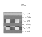
- A-1. 1 is a schematic cross-sectional view of a light control device according to one embodiment of the present invention.
- the light control element 100a shown in FIG. 1 is an electric field drive type light control element, and includes a glass film 10, a light control layer 20, a resin film 30, and an adhesive layer 40 in this order.
- the light control element 100 a further includes transparent electrode layers 50 a and 50 b for applying a voltage to the light control layer 20 between the glass film 10 and the light control layer 20 and between the light control layer 20 and the resin film 30.
- the light control layer 20 includes, for example, a liquid crystal compound or an electrochromic material.
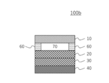
- FIG. 2 is a schematic cross-sectional view of a light control device according to another embodiment of the present invention.
- a dimming element 100b shown in FIG. 2 is a gaschromic dimming element, and includes a glass film 10, a dimming layer 20, a resin film 30, and an adhesive layer 40 in this order.
- the light control element 100b has the space
- the spacer 60 may be omitted as long as a space for introducing the gas is secured.
- the light control layer 20 includes a gas chromic material.
- the light control device of the present invention may be a light control device of a different system (for example, thermochromic system, photochromic system) from the illustrated example.
- the peeling film may be laminated
- the thickness of the light control element is, for example, 70 ⁇ m to 500 ⁇ m, preferably 80 ⁇ m to 450 ⁇ m, more preferably 100 ⁇ m to 400 ⁇ m, and further preferably 140 ⁇ m to 400 ⁇ m. .
- the bending radius of the light control element is, for example, 20 mm to 100 mm, preferably 20 mm to 90 mm, and more preferably 20 mm to 80 mm. Since the light control element which has the bending radius in the said range is excellent in flexibility, it can wind in a roll shape and can form a film roll. Moreover, workability
- A-2. Glass film Any appropriate glass film can be adopted. Examples of the glass constituting the glass film include soda-lime glass, borate glass, aluminosilicate glass, and quartz glass according to the classification by composition. Moreover, according to the classification
- the content of alkali metal components (for example, Na 2 O, K 2 O, Li 2 O) in the glass is preferably 15% by weight or less, and more preferably 10% by weight or less.
- the total light transmittance of the glass film is, for example, 80% or more, preferably 85% or more, and more preferably 90% or more.
- the thickness of the glass film is, for example, 50 ⁇ m to 200 ⁇ m, preferably 50 ⁇ m to 180 ⁇ m. If the thickness of the glass film is less than 50 ⁇ m, the impact resistance may be insufficient. On the other hand, if the thickness of the glass film exceeds 200 ⁇ m, the flexibility decreases, and the weight increases, so that the workability when affixing to the glass surface or the like can be decreased.
- thermoplastic resin examples include polyester resins such as PET; cycloolefin resins such as polynorbornene; acrylic resins; polycarbonate resins; and cellulose resins. Of these, polyester resins, cycloolefin resins, and acrylic resins are preferable. These resins are excellent in transparency, mechanical strength, thermal stability, moisture shielding properties and the like. You may use the said thermoplastic resin individually or in combination of 2 or more types. Moreover, it is also possible to use an optical film used for a polarizing plate, for example, a low retardation substrate, a high retardation substrate, a retardation plate, a brightness enhancement film, and the like.
- the elastic modulus (tensile elastic modulus) at 23 ° C. of the resin film is preferably 2 GPa to 10 GPa, preferably 2 GPa to 6 GPa. According to the resin film having an elastic modulus within the above range, a highly brittle glass material is favorably supported, and as a result, a light control element having excellent flexibility can be obtained.
- the thickness of the resin film is preferably 20 ⁇ m to 200 ⁇ m, more preferably 30 ⁇ m to 200 ⁇ m, and even more preferably 30 ⁇ m to 150 ⁇ m. According to the resin film having a thickness within the above range, a highly brittle glass material can be favorably supported, and the thickness of the light control element can be reduced, so that a light control element having excellent flexibility can be obtained.
- the total light transmittance of the resin film is preferably 60% or more, more preferably 70% or more, and further preferably 80% or more.
- Light control layer A-4-1 Light control layer containing a liquid crystal compound
- the light control layer containing a liquid crystal compound is typically constituted by dispersing a liquid crystal compound in a polymer matrix. In the light control layer, it is possible to switch between the light transmission state and the light scattering state by changing the orientation degree of the liquid crystal compound depending on the presence or absence of voltage application.
- the light control layer is in a light transmission state when a voltage is applied, and is in a light scattering state when no voltage is applied (normal mode).
- the liquid crystal compound when the voltage is not applied, the liquid crystal compound is not oriented, so that the light scattering state occurs.
- the liquid crystal compound is oriented so that the refractive index of the liquid crystal compound and the refractive index of the polymer matrix are As a result, the light transmission state is obtained.
- the light control layer enters a light scattering state when a voltage is applied, and enters a light transmission state when no voltage is applied (reverse mode).
- the alignment film provided on the surface of the transparent electrode layer aligns the liquid crystal compound when no voltage is applied and enters a light transmission state, and the application of the voltage disturbs the alignment of the liquid crystal compound and causes a light scattering state.
- Examples of the light control layer as described above include a light control layer including a polymer dispersed liquid crystal, a light control layer including a polymer network type liquid crystal, and the like.
- the polymer-dispersed liquid crystal has a structure in which liquid crystal compounds in the form of droplets are dispersed in a polymer matrix.
- the polymer network type liquid crystal has a structure in which a liquid crystal compound is dispersed in a polymer network, and the liquid crystal in the polymer network has a continuous phase.
- any appropriate non-polymerizable liquid crystal compound is used as the liquid crystal compound.
- the dielectric anisotropy of the liquid crystal compound may be positive or negative.
- the liquid crystal compound can be, for example, a nematic type, a smectic type, or a cholesteric type liquid crystal compound. It is preferable to use a nematic liquid crystal compound because excellent transparency can be realized in a light transmission state.
- nematic liquid crystal compounds examples include biphenyl compounds, phenylbenzoate compounds, cyclohexylbenzene compounds, azoxybenzene compounds, azobenzene compounds, azomethine compounds, terphenyl compounds, biphenylbenzoate compounds, cyclohexylbiphenyl compounds. , Phenylpyridine compounds, cyclohexylpyrimidine compounds, cholesterol compounds, fluorine compounds, and the like.
- the content of the liquid crystal compound in the light control layer is, for example, 40% by weight or more, preferably 50% by weight to 99% by weight, and more preferably 50% by weight to 95% by weight.
- the resin forming the polymer matrix can be appropriately selected according to the light transmittance, the refractive index of the liquid crystal compound, and the like. It may be a light isotropic resin or a light anisotropic resin.
- the resin is an active energy ray curable resin, for example, a liquid crystal polymer obtained by curing a polymerizable liquid crystal compound, a (meth) acrylic resin, a silicone resin, an epoxy resin, a fluorine resin. Resins, polyester resins, polyimide resins and the like can be preferably used.
- the content of the polymer matrix in the light control layer is preferably 1% by weight to 60% by weight, and more preferably 5% by weight to 50% by weight.
- the content of the polymer matrix is less than 1% by weight, problems such as low adhesion to the transparent conductive film may occur.
- problems such as an increase in driving voltage and a dimming function may occur.
- the thickness of the light control layer can be, for example, 10 ⁇ m to 100 ⁇ m, preferably 15 ⁇ m to 60 ⁇ m.
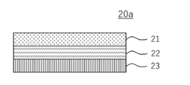
- FIG. 3 is a schematic cross-sectional view of an example of a light control layer including an electrochromic material that can be used in the present invention.
- the light control layer 20a containing an electrochromic material includes a first electrochromic compound layer 21 (first EC layer), an electrolyte layer 22, and a second electrochromic compound layer 23 (second EC layer) in this order.
- the thickness of the light control layer 20a is, for example, 0.1 ⁇ m to 400 ⁇ m, preferably 0.5 ⁇ m to 200 ⁇ m.
- the first EC layer is a dimming layer that changes its light transmittance and color according to the current flowing in the first EC layer together with the second EC layer described later.
- the electrochromic compound for forming the first EC layer is not limited.
- inorganic electrochromic such as tungsten oxide (for example, WO 3 ), molybdenum oxide, vanadium oxide, indium oxide, iridium oxide, nickel oxide, Prussian blue, etc.
- Compounds for example, organic electrochromic compounds such as phthalocyanine compounds, styryl compounds, viologen compounds, polypyrrole, polyaniline, polythiophene (for example, poly (ethylenedioxythiophene) -poly (styrenesulfonic acid)), etc.
- tungsten oxide and polythiophene are used.
- the thickness of the first EC layer 10 is, for example, 0.01 ⁇ m or more, preferably 0.05 ⁇ m or more, and for example, 40 ⁇ m or less, preferably 20 ⁇ m or less.
- the electrolyte layer is a layer for efficiently energizing the electrochromic compound inside the first EC layer and the second EC layer.
- the electrolyte layer may be formed from a liquid electrolyte and a sealing material that seals the liquid electrolyte, or may be formed from a solid electrolyte membrane.
- the electrolyte that forms the electrolyte layer is not limited.
- LiClO 4 , LiBF 4 , LiAsF 6 , LiPF 6 , LiCF 3 SO 3 , LiCF 3 COO, KCl, NaClO 3 , NaCl, NaBF 4 , NaSCN, KBF 4 examples thereof include alkali metal salts or alkaline earth metal salts such as Mg (ClO 4 ) 2 and Mg (BF 4 ) 2 .
- a quaternary ammonium salt, a quaternary phosphonium salt, etc. are mentioned.
- an organic solvent is preferably used together with the electrolyte.
- the organic solvent is not limited as long as it can dissolve the electrolyte, carbonates such as ethylene carbonate, propylene carbonate, and methyl carbonate; for example, furans such as tetrahydrofuran; for example, ⁇ -butyrolactone, 1,2-dimethoxyethane, Examples include 1,3-dioxolane, 4-methyl-1,3-dioxolane, methyl formate, methyl acetate, methyl propionate, acetonitrile, propylene carbonate, N, N-dimethylformamide and the like.
- the electrolyte layer is preferably an electrolyte membrane containing an electrolyte, an organic solvent, and a binder resin.
- Such an electrolyte layer can be obtained, for example, by mixing an electrolyte solution in which an electrolyte is dissolved in an organic solvent and a binder resin, and drying.
- binder resin examples include acrylic resins such as polymethyl methacrylate.
- the thickness of the electrolyte layer is, for example, 0.01 ⁇ m or more, preferably 0.1 ⁇ m or more, and for example, 300 ⁇ m or less, preferably 100 ⁇ m or less.
- the same explanation as the first EC layer can be applied to the second EC layer.
- the second EC layer may have the same configuration as the first EC layer or a different configuration.
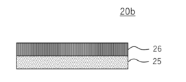
- FIG. 4 is a schematic cross-sectional view of an example of a light control layer containing a gas chromic material that can be used in the present invention.
- the light control layer 20 b containing a gas chromic material includes a gas chromic compound layer 25 (GC layer) and a catalyst layer 26.
- the light control layer 20b containing the gas chromic material is typically disposed so that the catalyst layer 26 is in contact with the gas (on the gap side).
- the GC layer includes a chromic material whose state reversibly changes between a transparent state by hydrogenation and a reflection state by dehydrogenation.
- the chromic material constituting the GC layer include rare earth metals such as Y, La, Gd and Sm, alloys of rare earth metals and magnesium, alloys of alkaline earth metals such as Ca, Sr and Ba, magnesium, Ni, Examples include alloys of transition metals such as Mn, Co, and Fe and magnesium.
- the GC layer preferably contains magnesium because of its excellent transparency during hydrogenation, and a rare earth metal element-magnesium alloy is more preferred from the viewpoint of achieving both transparency and durability. Note that the GC layer may contain an element other than the alloy as a trace component.
- the above metal or alloy constituting the GC layer contains a metal element that becomes transparent by hydrogenation and becomes reflective by releasing hydrogen.
- a metal element that becomes transparent by hydrogenation and becomes reflective by releasing hydrogen For example, magnesium becomes transparent MgH 2 when hydrogenated, and becomes Mg having metal reflection by dehydrogenation.
- the thickness of the GC layer is not particularly limited, but is preferably 10 nm to 500 nm, more preferably 15 nm to 200 nm, and more preferably 20 nm from the viewpoint of achieving both the light transmittance in the transparent state and the light shielding rate (reflectance) in the reflective state. More preferably, it is ⁇ 100 nm. If the thickness of the GC layer is excessively small, the light reflectance in the reflective state tends to be low. Moreover, when the film thickness of the GC layer is excessively large, the light transmittance in a transparent state tends to be low.
- the catalyst layer has a function of promoting the hydrogenation and dehydrogenation of the GC layer.
- the material of the catalyst layer is not particularly limited as long as it has a function of promoting hydrogenation and dehydrogenation of the GC layer.
- the catalyst layer is selected from palladium, platinum, a palladium alloy, and a platinum alloy. It is preferred to have at least one metal.
- palladium is preferably used because of its high hydrogen permeability.
- the film thickness of the catalyst layer can be appropriately set depending on the reactivity of the GC layer, the catalyst capacity of the catalyst layer, and the like.
- the film thickness of the catalyst layer is, for example, 1 nm to 30 nm, preferably 2 nm to 20 nm. If the thickness of the catalyst layer is excessively small, the hydrogenation and dehydrogenation catalytic functions may not be sufficiently exhibited. Moreover, when the film thickness of a catalyst layer is too large, there exists a tendency for light transmittance to fall.
- the GC layer and the catalyst layer can be sequentially formed on the resin film by sputtering.
- the light control layer 20b containing a gas chromic material may further include layers other than the GC layer 25 and the catalyst layer 26 as necessary.
- a base layer may be provided on the side of the GC layer where the catalyst layer is not provided (for example, between the resin film and the GC layer), or a buffer layer may be provided between the GC layer and the catalyst layer.
- a surface layer may be provided on the catalyst layer.
- an inorganic oxide layer As a base layer between the resin film and the GC layer, moisture, oxygen gas, etc. generated from the resin film can be blocked and oxidation of the GC layer can be suppressed.
- a metal thin film made of Ti, Nb, V, or an alloy of these metals as a buffer layer between the GC layer and the catalyst layer, migration of magnesium and the like from the GC layer to the catalyst layer is suppressed.
- the switching speed from the transparent state to the reflective state due to dehydrogenation tends to increase.
- the surface layer may have a function of blocking permeation of water and oxygen and preventing oxidation of the GC layer.
- the material constituting the surface layer include inorganic materials such as inorganic oxides, organic materials such as polymers, and organic-inorganic hybrid materials.
- the transparent electrode layer transparent electrode layer such as indium tin oxide (ITO), zinc oxide (ZnO), may be formed using a metal oxide such as tin oxide (SnO 2).
- the first transparent electrode layer can be formed of a metal nanowire such as silver nanowire (AgNW), a carbon nanotube (CNT), an organic conductive film, a metal layer, or a laminate thereof.
- the first transparent electrode layer can be patterned into a desired shape according to the purpose.
- the total light transmittance of the transparent electrode layer is preferably 80% or more, more preferably 85% or more, and further preferably 90% or more.
- the surface resistance value of the transparent electrode layer is preferably 0.1 ⁇ / ⁇ to 1000 ⁇ / ⁇ , more preferably 0.5 ⁇ / ⁇ to 500 ⁇ / ⁇ , and further preferably 1 ⁇ / ⁇ to 250 ⁇ / ⁇ . .
- the thickness of the transparent electrode layer is preferably 0.01 ⁇ m to 0.06 ⁇ m, more preferably 0.01 ⁇ m to 0.045 ⁇ m. If it is such a range, the electrode layer excellent in electroconductivity and light transmittance can be obtained.
- the transparent electrode layer can be provided on a glass film or a resin film using a method such as sputtering.
- the transparent electrode layer may be directly formed on these films, and may be formed via a refractive index adjusting layer, a supporting base material, etc. as needed.
- Adhesive layer Any appropriate adhesive composition can be used as the adhesive composition constituting the adhesive layer.
- Specific examples of usable pressure-sensitive adhesive compositions include pressure-sensitive adhesive compositions based on (meth) acrylic polymers, silicone-based polymers, polyesters, polyurethanes, polyamides, polyethers, fluorine-based polymers, rubber-based polymers, and the like. Is mentioned. Among these, from the viewpoints of transparency, weather resistance, heat resistance and the like, an acrylic pressure-sensitive adhesive composition having an acrylic polymer as a base polymer is preferable.
- the pressure-sensitive adhesive composition may further contain any appropriate additive as required.
- the additive include a crosslinking agent, a tackifier, a plasticizer, a pigment, a dye, a filler, an anti-aging agent, a conductive material, an ultraviolet absorber, a light stabilizer, a release modifier, a softener, and a surfactant. , Flame retardants, antioxidants and the like.
- crosslinking agent isocyanate crosslinking agent, epoxy crosslinking agent, peroxide crosslinking agent, melamine crosslinking agent, urea crosslinking agent, metal alkoxide crosslinking agent, metal chelate crosslinking agent, metal salt crosslinking agent, A carbodiimide type crosslinking agent, an oxazoline type crosslinking agent, an aziridine type crosslinking agent, an amine type crosslinking agent, etc. are mentioned.
- the elastic modulus (storage elastic modulus) at 23 ° C. of the pressure-sensitive adhesive layer is preferably 1 ⁇ 10 ⁇ 5 GPa to 1 ⁇ 10 ⁇ 2 GPa, more preferably 5.0 ⁇ 10 ⁇ 5 GPa to 5.0 ⁇ 10 ⁇ . It can be 3 GPa, more preferably 1.0 ⁇ 10 ⁇ 4 GPa to 1.0 ⁇ 10 ⁇ 3 GPa.
- the pressure-sensitive adhesive layer having such an elastic modulus can contribute to improvement in impact resistance and workability at the time of attachment. Moreover, when it has an adhesive layer which has such an elasticity modulus, when a long light control element is wound in roll shape, it can function as an impact relaxation layer.
- the thickness (dry film thickness) of the pressure-sensitive adhesive layer is determined according to the desired pressure-sensitive adhesive force (peeling force).
- the thickness (dry film thickness) of the pressure-sensitive adhesive layer is preferably about 20 ⁇ m to 200 ⁇ m, more preferably 20 ⁇ m to 150 ⁇ m, and still more preferably 25 ⁇ m to 100 ⁇ m.
- the said light control element may be manufactured by arbitrary appropriate methods.
- the light control film for example, unwinds a long resin film with a transparent electrode layer having a transparent electrode layer formed on one side in advance from a roll; while transporting the resin film with a transparent electrode layer in the longitudinal direction, Applying a composition for forming a light control layer on the surface of the transparent electrode layer to form a coating layer; a long glass film with a transparent electrode layer having a transparent electrode layer previously formed on one side of the coating layer; , Forming a laminate by continuously laminating the transparent electrode layer facing the coating layer and aligning the longitudinal direction of each other; obtaining the light control film by curing the coating layer A separately prepared long release film with a pressure-sensitive adhesive layer is continuously laminated so that the pressure-sensitive adhesive layer faces the resin film surface of the light control film and aligns
- the composition for light control layer formation contains the monomer (preferably active energy ray hardening-type monomer) and liquid crystal compound for forming a polymer matrix, for example.
- a glass roll with a light control layer in one embodiment of the present invention comprises a long glass film having a thickness of 50 ⁇ m to 200 ⁇ m, a light control layer laminated on one side of the glass film, Have.
- the glass roll with a light control layer has a glass film, a light control layer, a resin film, and an adhesive layer in this order.
- the glass film, the light control layer, the resin film, and the pressure-sensitive adhesive layer those described in the section A are preferably used.
- the glass roll with a light control layer may be one in which the light control element described in the section A formed in a long shape is wound into a roll shape.
- the above-mentioned glass roll with a light control layer is lightweight and has high reliability (impact resistance, scratch resistance, etc.), and when it has an adhesive layer, it can be easily attached to the glass surface or the like.
- ⁇ Measurement method of elastic modulus> (Elastic modulus of resin film) A strip sample having a thickness of 50 ⁇ m, a width of 2 cm, and a length of 15 cm was prepared, and the elastic modulus was measured from the elongation and stress in the longitudinal direction of the strip sample using an autograph (manufactured by Shimadzu Corporation, AG-I). The test conditions were a distance between chucks of 10 cm and a pulling speed of 10 mm / min. (Elastic modulus of adhesive) The storage elastic modulus at 23 ° C. of the pressure-sensitive adhesive layer was measured using a viscoelasticity measuring device ARES (manufactured by TA Instruments).
- ARES viscoelasticity measuring device
- the pressure-sensitive adhesive layer was formed into a sheet having a thickness of 2 mm, punched out according to a parallel plate having a diameter of 25 mm, and attached to the chuck of the apparatus. Then, while applying strain at a period of 1 Hz, the temperature was increased from ⁇ 70 ° C. to 150 ° C. at a rate of temperature increase of 5 ° C./min, and the storage elastic modulus at 23 ° C. was measured. ⁇ Method for measuring thickness> Measurement was performed using a dial gauge.
- the acrylic polymer solution was prepared by carrying out the polymerization reaction for 10 hours.
- To 100 parts by weight of the solid content of the acrylic polymer solution 0.5 part by weight of an adduct of trimethylolpropane / tolylene diisocyanate (Nihon Polyurethane Kogyo Co., Ltd., Coronate L) as an isocyanate crosslinking agent, and a silane coupling agent ( 0.1 parts by weight of Shin-Etsu Chemical Co., Ltd. KBM403) was uniformly mixed and stirred to obtain an acrylic pressure-sensitive adhesive composition A.
- a transparent electrode layer is formed by sputtering on one side of a transparent PET base material (Mitsubishi Chemical Co., Ltd., “Diafoil”, thickness: 188 ⁇ m, elastic modulus: 4.0 GPa) to obtain a PET film with an electrode layer It was.
- a transparent electrode layer (ITO layer) was formed on one side of a glass film (Nippon Electric Glass Co., Ltd., “OA-10G”, thickness: 150 ⁇ m) by sputtering to obtain a glass film with an electrode layer.
- a release film with a pressure-sensitive adhesive layer was obtained by applying the pressure-sensitive adhesive composition A to a release-treated surface of a PET film that had been subjected to a release treatment on one side, and drying it.
- the pressure-sensitive adhesive layer had a thickness of 50 ⁇ m and an elastic modulus of 4 ⁇ 10 ⁇ 4 GPa.
- a light control layer comprising a PET film with an electrode layer and a glass film with an electrode layer, comprising nematic liquid crystal molecules and 1,6-hexanediol diacrylate (manufactured by Nippon Kayaku Co., Ltd., “HDDA”) )
- the polymer-dispersed liquid crystal layer forming composition was cured to obtain a laminate.
- the said peeling film with an adhesive layer was laminated
- a light control device having a configuration of [glass film / transparent electrode layer / light control layer / transparent electrode layer / resin film / adhesive layer / release film] was obtained.
- the thickness from the glass film to the pressure-sensitive adhesive layer was 408 ⁇ m.
- Example 2 A transparent PET substrate (“Diafoil”, thickness: 50 ⁇ m, elastic modulus: 4.0 GPa) manufactured by Mitsubishi Chemical Corporation was used as the resin film, and a glass film (manufactured by Nippon Electric Glass Co., Ltd., “ OA-10G ”(thickness: 100 ⁇ m) was used in the same manner as in Example 1 except that [glass film / transparent electrode layer / light control layer / transparent electrode layer / resin film / adhesive layer / release film] The light control element which has a structure was obtained. The thickness from the glass film to the pressure-sensitive adhesive layer was 220 ⁇ m.
- Example 3 A transparent PET substrate (“Diafoil”, manufactured by Mitsubishi Chemical Corporation, thickness: 50 ⁇ m, elastic modulus: 4.0 GPa) was used as the resin film, and a glass film (manufactured by Nippon Electric Glass Co., Ltd., “OA-”). 10G ", thickness: 70 ⁇ m), and the thickness of the pressure-sensitive adhesive layer was changed to 20 ⁇ m, in the same manner as in Example 1, [Glass film / transparent electrode layer / light control layer / transparent electrode layer / A light control element having a structure of “resin film / adhesive layer / release film” was obtained. The thickness from the glass film to the pressure-sensitive adhesive layer was 160 ⁇ m.
- Example 1 [Glass film / transparent electrode layer / light control layer / transparent] In the same manner as in Example 1 except that a glass film (manufactured by Nippon Electric Glass Co., Ltd., “OA-10G”, thickness: 300 ⁇ m) was used as the glass film.
- the light control element which has the structure of an electrode layer / resin film / adhesive layer / release film] was obtained.
- the thickness from the glass film to the pressure-sensitive adhesive layer was 558 ⁇ m.
- a transparent PET substrate (Made by Mitsubishi Chemical, “Diafoil”, thickness: 50 ⁇ m, elastic modulus: 4.0 GPa) was used as the resin film, and a transparent PET substrate (Mitsubishi Chemical Corporation, “ [Diafoil], thickness: 100 ⁇ m), and the thickness of the pressure-sensitive adhesive layer was changed to 20 ⁇ m, in the same manner as in Example 1, [first resin film / transparent electrode layer / light control layer / A light control device having a configuration of transparent electrode layer / second resin film / adhesive layer / release film] was obtained. The thickness from the first resin film to the pressure-sensitive adhesive layer was 190 ⁇ m.
- Example 3 A transparent PET base material (manufactured by Mitsubishi Chemical Corporation, “Diafoil”, thickness: 300 ⁇ m, elastic modulus: 4.0 GPa) was used as the resin film, and a glass film (manufactured by Nippon Electric Glass Co., Ltd., “ OA-10G ”(thickness: 100 ⁇ m) was used in the same manner as in Example 1 except that [glass film / transparent electrode layer / light control layer / transparent electrode layer / resin film / adhesive layer / release film] The light control element which has a structure was obtained. The thickness from the glass film to the pressure-sensitive adhesive layer was 470 ⁇ m.
- a transparent PET substrate (“Diafoil”, thickness: 50 ⁇ m, elastic modulus: 4.0 GPa) manufactured by Mitsubishi Chemical Corporation was used as the resin film, and a glass film (manufactured by Nippon Electric Glass Co., Ltd., “ [Glass film / transparent electrode layer / light control layer / transparent electrode], in the same manner as in Example 1, except that OA-10G ”and thickness: 35 ⁇ m) were used, and the thickness of the pressure-sensitive adhesive layer was 20 ⁇ m.
- the light control device of the example is good in both impact resistance and scratch resistance and has high reliability. Moreover, since the exposed surface when it affixes on a window etc. is a glass surface, it can be excellent also in durability. Furthermore, since it is lightweight and has an appropriate flexibility, the workability at the time of pasting was also excellent. On the other hand, the light control element of the comparative example has a problem in workability at the time of pasting as a result of either insufficient shock resistance or scratch resistance or insufficient flexibility. there were.
- the present invention is suitably used in the field of light control films.
Landscapes
- Physics & Mathematics (AREA)
- Nonlinear Science (AREA)
- General Physics & Mathematics (AREA)
- Optics & Photonics (AREA)
- Chemical & Material Sciences (AREA)
- Mathematical Physics (AREA)
- Crystallography & Structural Chemistry (AREA)
- Organic Chemistry (AREA)
- Laminated Bodies (AREA)
- Liquid Crystal (AREA)
- Electrochromic Elements, Electrophoresis, Or Variable Reflection Or Absorption Elements (AREA)
- Electroluminescent Light Sources (AREA)
- Surface Treatment Of Glass (AREA)
- Glass Compositions (AREA)
- Window Of Vehicle (AREA)
Abstract
Description
1つの実施形態において、上記樹脂フィルムの厚みが、20μm~200μmであり、上記樹脂フィルムの23℃における弾性率が、2GPa~10GPaである。
1つの実施形態において、上記粘着剤層の厚みが、20μm~200μmであり、上記粘着剤層の23℃における弾性率が、1×10⁻⁵GPa~1×10⁻²GPaである。
1つの実施形態において、上記調光素子のガラスフィルムから粘着剤層までの厚みが、70μm~500μmである。
本発明のさらに別の局面によれば、長尺状のガラスフィルムと、該ガラスフィルムの片側に積層された調光層と、を有し、該ガラスフィルムの厚みが、50μm~200μmである、調光層付ガラスフィルムロールが提供される。
本発明の調光素子は、ガラスフィルムと、調光層と、樹脂フィルムと、粘着剤層と、をこの順に備える。調光層を挟持する2枚の基材中、ガラス表面等に貼り合わせる方の基材を樹脂フィルムとし、他方を薄いガラスフィルムとすることにより、調光素子の露出面に耐擦傷性、耐衝撃性等の信頼性を付与するとともに軽量化を実現できる。また、本発明の調光素子は、可とう性を有することからロール状に巻回することができ、さらに、軽量で粘着剤層を備えることから、簡便にガラス表面等に貼り付けることができる。
図1は、本発明の1つの実施形態における調光素子の概略断面図である。図1に示す調光素子100aは、電界駆動方式の調光素子であり、ガラスフィルム10と、調光層20と、樹脂フィルム30と、粘着剤層40と、をこの順に備える。調光素子100aは、ガラスフィルム10と調光層20との間および調光層20と樹脂フィルム30との間に、調光層20に電圧を印加するための透明電極層50a、50bをさらに備える。当該実施形態において、調光層20は、例えば、液晶化合物またはエレクトロクロミック材料を含む。
ガラスフィルムは、任意の適切なものが採用され得る。ガラスフィルムを構成するガラスとしては、組成による分類によれば、例えば、ソーダ石灰ガラス、ホウ酸ガラス、アルミノ珪酸ガラス、石英ガラス等が挙げられる。また、アルカリ成分による分類によれば、無アルカリガラス、低アルカリガラスが挙げられる。
樹脂フィルムの構成材料は、代表的には熱可塑性樹脂である。熱可塑性樹脂としては、例えば、PET等のポリエステル系樹脂;ポリノルボルネン等のシクロオレフィン系樹脂;アクリル系樹脂;ポリカーボネート樹脂;セルロース系樹脂等が挙げられる。なかでも好ましくは、ポリエステル系樹脂、シクロオレフィン系樹脂またはアクリル系樹脂である。これらの樹脂は、透明性、機械的強度、熱安定性、水分遮蔽性等に優れる。上記熱可塑性樹脂は、単独で、または2種以上組み合わせて用いてもよい。また、偏光板に用いられるような光学フィルム、例えば、低位相差基材、高位相差基材、位相差板、輝度向上フィルム等を用いることも可能である。
A-4-1.液晶化合物を含む調光層
液晶化合物を含む調光層は、代表的には、高分子マトリクス中に液晶化合物を分散させて構成される。該調光層においては、電圧印加の有無により、液晶化合物の配向度を変化させて、光透過状態と光散乱状態とを切替えることができる。
図3は、本発明で用いられ得るエレクトロクロミック材料を含む調光層の一例の概略断面図である。エレクトロクロミック材料を含む調光層20aは、第1エレクトロクロミック化合物層21(第1EC層)と、電解質層22と、第2エレクトロクロミック化合物層23(第2EC層)とをこの順に備える。調光層20aの厚みは、例えば0.1μm~400μm、好ましくは0.5μm~200μmである。
透明電極層は、例えば、インジウム錫酸化物(ITO)、酸化亜鉛(ZnO)、酸化錫(SnO2)等の金属酸化物を用いて形成され得る。あるいは、第1の透明電極層は、銀ナノワイヤー(AgNW)等の金属ナノワイヤ、カーボンナノチューブ(CNT)、有機導電膜、金属層またはこれらの積層体によって形成され得る。第1の透明電極層は、目的に応じて、所望の形状にパターニングされ得る。
粘着剤層を構成する粘着剤組成物としては、任意の適切な粘着剤組成物が用いられ得る。使用可能な粘着剤組成物の具体例としては、(メタ)アクリル系ポリマー、シリコーン系ポリマー、ポリエステル、ポリウレタン、ポリアミド、ポリエーテル、フッ素系ポリマー、ゴム系ポリマー等をベースポリマーとする粘着剤組成物が挙げられる。なかでも、透明性、耐候性、耐熱性等の観点から、アクリル系ポリマーをベースポリマーとするアクリル系粘着剤組成物が好ましい。
上記調光素子は任意の適切な方法によって製造され得る。以下、調光層が液晶化合物を含む調光素子をロールトゥロール方式で製造する場合について例示的に説明する。調光フィルムは、例えば、予め片面に透明電極層が形成された長尺状の透明電極層付樹脂フィルムをロールから巻出すこと;該透明電極層付樹脂フィルムを長手方向に搬送しながら、その透明電極層面に、調光層形成用組成物を塗布して塗布層を形成すること;該塗布層上に、予め片面に透明電極層が形成された長尺状の透明電極層付ガラスフィルムを、その透明電極層が塗布層に対向するように、かつ、互いの長尺方向を揃えて連続的に積層して積層体を形成すること;該塗布層を硬化させて調光フィルムを得ること;別途に用意した長尺状の粘着剤層付剥離フィルムを、粘着剤層が調光フィルムの樹脂フィルム面に対向するように、かつ、互いの長尺方向を揃えて連続的に積層して調光素子を得ること;および、得られた調光素子をロール状に巻き取ること;を含む方法によって得ることができる。このとき、調光層形成用組成物は、例えば、高分子マトリクスを形成するためのモノマー(好ましくは、活性エネルギー線硬化型モノマー)および液晶化合物を含む。
本発明の1つの実施形態における調光層付ガラスロールは、厚みが50μm~200μmである長尺状のガラスフィルムと、該ガラスフィルムの片側に積層された調光層と、を有する。代表的には、調光層付ガラスロールは、ガラスフィルムと、調光層と、樹脂フィルムと、粘着剤層とをこの順に有する。ガラスフィルム、調光層、樹脂フィルムおよび粘着剤層としてはそれぞれ、A項で説明したものが好ましく用いられる。上記調光層付ガラスロールは、長尺状に形成されたA項に記載の調光素子がロール状に巻回されたものであってもよい。
(樹脂フィルムの弾性率)
厚み50μm、幅2cm、長さ15cmの短冊状サンプルを作製し、オートグラフ(島津製作所社製、AG-I)を用いて、短冊状サンプルの長手方向の伸びと応力から弾性率を測定した。試験条件は、チャック間距離を10cm、引っ張り速度を10mm/minとした。
(粘着剤の弾性率)
粘弾性測定装置ARES(TAインスツルメント社製)を使用して、粘着剤層の23℃における貯蔵弾性率を測定した。すなわち、粘着剤層を厚み2mmのシート状に成形し、これを直径25mmのパラレルプレートに合わせて打ち抜き、装置のチャックに装着した。そして、1Hzの周期でひずみを与えつつ、5℃/分の昇温速度で-70℃から150℃まで温度を上昇させて、23℃のときの貯蔵弾性率を測定した。
<厚みの測定方法>
ダイヤルゲージを用いて測定した。
攪拌羽根、温度計、窒素ガス導入管、冷却器を備えた四つ口フラスコに、ブチルアクリレート100重量部、アクリル酸5重量部および2-ヒドロキシエチルアクリレート0.1重量部、重合開始剤として2,2’-アゾビスイソブチロニトリル0.2重量部、重合溶媒として酢酸エチル200重量部を仕込み、十分に窒素置換した後、窒素気流下で撹拌しながらフラスコ内の液温を55℃付近に保って10時間重合反応を行い、アクリル系ポリマー溶液を調製した。
上記アクリル系ポリマー溶液の固形分100重量部に、イソシアネート系架橋剤としてトリメチロールプロパン/トリレンジイソシアネートのアダクト体(日本ポリウレタン工業社製、コロネートL)0.5重量部と、シランカップリング剤(信越化学工業社製、KBM403)0.1重量部を、均一に混合撹拌して、アクリル系粘着剤組成物Aを得た。
透明PET基材(三菱ケミカル社製、「ダイヤホイル」、厚み:188μm、弾性率:4.0GPa)の片面にスパッタにより透明電極層(ITO層)を形成して、電極層付PETフィルムを得た。
ガラスフィルム(日本電気硝子社製、「OA-10G」、厚み:150μm)の片面にスパッタにより透明電極層(ITO層)を形成して、電極層付ガラスフィルムを得た。
片面に剥離処理が施されているPETフィルムの剥離処理面に、粘着剤組成物Aを塗布し乾燥させることにより粘着剤層付剥離フィルムを得た。粘着剤層の厚みは50μmであり、その弾性率は4×10⁻⁴GPaであった。
電極層付PETフィルムと電極層付ガラスフィルムとを、ネマティック液晶分子と1,6-ヘキサンジオールジアクリレート(日本化薬社製、「HDDA」)とを含む調光層(高分子分散型液晶層)形成用組成物を介して、ITO層が対向するようにして貼り合わせた後、高分子分散型液晶層形成用組成物を硬化させて、積層体を得た。
次いで、上記粘着剤層付剥離フィルムを、粘着剤層がPETフィルムと対向するように調光フィルムに積層した。
以上のようにして、[ガラスフィルム/透明電極層/調光層/透明電極層/樹脂フィルム/粘着剤層/剥離フィルム]の構成を有する調光素子を得た。ガラスフィルムから粘着剤層までの厚みは、408μmであった。
樹脂フィルムとして透明PET基材(三菱ケミカル社製、「ダイヤホイル」、厚み:50μm、弾性率:4.0GPa)を用いたこと、および、ガラスフィルムとして、ガラスフィルム(日本電気硝子社製、「OA-10G」、厚み:100μm)を用いたこと以外は実施例1と同様にして、[ガラスフィルム/透明電極層/調光層/透明電極層/樹脂フィルム/粘着剤層/剥離フィルム]の構成を有する調光素子を得た。ガラスフィルムから粘着剤層までの厚みは、220μmであった。
樹脂フィルムとして透明PET基材(三菱ケミカル社製、「ダイヤホイル」、厚み:50μm、弾性率:4.0GPa)を用いたこと、ガラスフィルムとして、ガラスフィルム(日本電気硝子社製、「OA-10G」、厚み:70μm)を用いたこと、および、粘着剤層の厚みを20μmにしたこと以外は実施例1と同様にして、[ガラスフィルム/透明電極層/調光層/透明電極層/樹脂フィルム/粘着剤層/剥離フィルム]の構成を有する調光素子を得た。ガラスフィルムから粘着剤層までの厚みは、160μmであった。
ガラスフィルムとして、ガラスフィルム(日本電気硝子社製、「OA-10G」、厚み:300μm)を用いたこと以外は実施例1と同様にして、[ガラスフィルム/透明電極層/調光層/透明電極層/樹脂フィルム/粘着剤層/剥離フィルム]の構成を有する調光素子を得た。ガラスフィルムから粘着剤層までの厚みは、558μmであった。
樹脂フィルムとして透明PET基材(三菱ケミカル社製、「ダイヤホイル」、厚み:50μm、弾性率:4.0GPa)を用いたこと、ガラスフィルムの代わりに透明PET基材(三菱ケミカル社製、「ダイヤホイル」、厚み:100μm)を用いたこと、および、粘着剤層の厚みを20μmにしたこと以外は実施例1と同様にして、[第1の樹脂フィルム/透明電極層/調光層/透明電極層/第2の樹脂フィルム/粘着剤層/剥離フィルム]の構成を有する調光素子を得た。第1の樹脂フィルムから粘着剤層までの厚みは、190μmであった。
樹脂フィルムとして透明PET基材(三菱ケミカル社製、「ダイヤホイル」、厚み:300μm、弾性率:4.0GPa)を用いたこと、および、ガラスフィルムとして、ガラスフィルム(日本電気硝子社製、「OA-10G」、厚み:100μm)を用いたこと以外は実施例1と同様にして、[ガラスフィルム/透明電極層/調光層/透明電極層/樹脂フィルム/粘着剤層/剥離フィルム]の構成を有する調光素子を得た。ガラスフィルムから粘着剤層までの厚みは、470μmであった。
樹脂フィルムとして透明PET基材(三菱ケミカル社製、「ダイヤホイル」、厚み:50μm、弾性率:4.0GPa)を用いたこと、および、ガラスフィルムとして、ガラスフィルム(日本電気硝子社製、「OA-10G」、厚み:35μm)を用いたこと、および、粘着剤層の厚みを20μmにしたこと以外は実施例1と同様にして、[ガラスフィルム/透明電極層/調光層/透明電極層/樹脂フィルム/粘着剤層/剥離フィルム]の構成を有する調光素子を得た。ガラスフィルムから粘着剤層までの厚みは、125μmであった。
<曲げ半径>
20mmから100mmまでの半径となるように10mmずつ半径が異なる複数の塩化ビニル製のポールを準備した。23℃の環境下、剥離フィルムを剥がした調光素子サンプルをガラスフィルム側(比較例2においては、第1の樹脂フィルム側)を外側にして、ポールに沿って沿わせ、セロハンテープ(ニチバン社製「CT405AP-24」、粘着力3.93N/10cm)を用いて両辺を固定可能・不可能かまたは割れるかで屈曲度合を確認し、割れることなく両辺を固定化能であったポールの最小半径を曲げ半径とした。なお、サンプルサイズは短辺20mm、長辺はポール外径の半径とした。
5cm×5cmサイズの調光素子から剥離フィルムを剥がしてガラス板に貼りつけ、評価サンプルとした。突き刺し棒(Φ0.5mm)を高さ10cmから20mm/minの速度でサンプルに落下させて、ガラスフィルムの割れを観察し、下記基準に従って評価した。
良好:割れなし
不良:割れあり
直径25mmの円柱の平滑な断面に、スチールウール#1000を均一に取り付けた。その上に、調光素子サンプルをガラスフィルム側表面(比較例2においては、第1の樹脂フィルム側表面)がスチールウールに接するように配置し、荷重1.5kgにて毎秒約100mmの速度で30往復させた後に、下記基準により目視評価にて判定した。
良好:キズが全くない。または細かなキズはあるが、視認性に影響はない
不良:明らかキズがあり、視認性を損なう

10 ガラスフィルム
20 調光層
30 樹脂フィルム
40 粘着剤層
Claims (5)
- ガラスフィルムと、調光層と、樹脂フィルムと、粘着剤層と、をこの順に備え、
曲げ半径が、20mm~100mmであり、
該ガラスフィルムの厚みが、50μm~200μmである、調光素子。 - 前記樹脂フィルムの厚みが、20μm~200μmであり、
前記樹脂フィルムの23℃における弾性率が、2GPa~10GPaである、請求項1に記載の調光素子。 - 前記粘着剤層の厚みが、20μm~200μmであり、
前記粘着剤層の23℃における弾性率が、1×10⁻⁵GPa~1×10⁻²GPaである、請求項1または2に記載の調光素子。 - 前記ガラスフィルムから前記粘着剤層までの厚みが、70μm~500μmである、請求項1から3のいずれかに記載の調光素子。
- 長尺状のガラスフィルムと、該ガラスフィルムの片側に積層された調光層と、を有し、
該ガラスフィルムの厚みが、50μm~200μmである、調光層付ガラスフィルムロール。
Priority Applications (5)
| Application Number | Priority Date | Filing Date | Title |
|---|---|---|---|
| US16/979,633 US11143892B2 (en) | 2018-03-28 | 2019-03-22 | Dimming element including glass film |
| EP19775974.9A EP3779577B1 (en) | 2018-03-28 | 2019-03-22 | Dimming element including glass film |
| KR1020207026079A KR102865558B1 (ko) | 2018-03-28 | 2019-03-22 | 유리 필름을 포함하는 조광 소자 |
| JP2020509930A JP7274458B2 (ja) | 2018-03-28 | 2019-03-22 | ガラスフィルムを含む調光素子 |
| CN201980021085.2A CN111902769B (zh) | 2018-03-28 | 2019-03-22 | 包含玻璃膜的调光元件 |
Applications Claiming Priority (2)
| Application Number | Priority Date | Filing Date | Title |
|---|---|---|---|
| JP2018-061556 | 2018-03-28 | ||
| JP2018061556 | 2018-03-28 |
Publications (1)
| Publication Number | Publication Date |
|---|---|
| WO2019188736A1 true WO2019188736A1 (ja) | 2019-10-03 |
Family
ID=68060032
Family Applications (1)
| Application Number | Title | Priority Date | Filing Date |
|---|---|---|---|
| PCT/JP2019/011955 Ceased WO2019188736A1 (ja) | 2018-03-28 | 2019-03-22 | ガラスフィルムを含む調光素子 |
Country Status (7)
| Country | Link |
|---|---|
| US (1) | US11143892B2 (ja) |
| EP (1) | EP3779577B1 (ja) |
| JP (1) | JP7274458B2 (ja) |
| KR (1) | KR102865558B1 (ja) |
| CN (1) | CN111902769B (ja) |
| TW (1) | TWI822743B (ja) |
| WO (1) | WO2019188736A1 (ja) |
Cited By (2)
| Publication number | Priority date | Publication date | Assignee | Title |
|---|---|---|---|---|
| WO2020129690A1 (ja) * | 2018-12-17 | 2020-06-25 | 日東電工株式会社 | 調光フィルム |
| JP7596897B2 (ja) | 2021-03-31 | 2024-12-10 | 株式会社リコー | エレクトロクロミック素子 |
Families Citing this family (2)
| Publication number | Priority date | Publication date | Assignee | Title |
|---|---|---|---|---|
| WO2023156941A1 (en) * | 2022-02-16 | 2023-08-24 | Agp Worldwide Operations Gmbh | Variable light transmission glazing with high complexity curvature |
| CN114942553B (zh) * | 2022-05-18 | 2023-11-14 | 京东方科技集团股份有限公司 | 显示基板及其控制方法和显示装置 |
Citations (6)
| Publication number | Priority date | Publication date | Assignee | Title |
|---|---|---|---|---|
| WO2008075773A1 (ja) * | 2006-12-21 | 2008-06-26 | Hitachi Chemical Co., Ltd. | 調光フィルム及び調光ガラス |
| JP2013148687A (ja) * | 2012-01-19 | 2013-08-01 | Konica Minolta Inc | 調光フィルム、及び調光フィルムの製造方法 |
| JP2015071284A (ja) | 2013-09-09 | 2015-04-16 | アキレス株式会社 | 調光自己粘着積層体 |
| CN106082711A (zh) * | 2016-06-02 | 2016-11-09 | 中国科学院广州能源研究所 | 一种智能调光节能夹层玻璃及其制备方法 |
| JP2017092033A (ja) * | 2015-11-09 | 2017-05-25 | 日東電工株式会社 | 光透過性導電フィルムおよび調光フィルム |
| WO2017099167A1 (ja) * | 2015-12-09 | 2017-06-15 | 旭硝子株式会社 | 合わせガラス |
Family Cites Families (28)
| Publication number | Priority date | Publication date | Assignee | Title |
|---|---|---|---|---|
| US4268134A (en) * | 1979-03-07 | 1981-05-19 | Corning Glass Works | Lightweight laminated photochromic lenses |
| JPH04130311A (ja) * | 1990-09-21 | 1992-05-01 | Dainippon Ink & Chem Inc | 液晶デバイス及びその製造方法 |
| JPH08201780A (ja) * | 1995-01-20 | 1996-08-09 | Alps Electric Co Ltd | 液晶表示媒体 |
| JP3706105B2 (ja) * | 2001-03-15 | 2005-10-12 | 三井化学株式会社 | ディスプレイ用フィルタおよびそれを用いた表示装置 |
| JP4060249B2 (ja) * | 2003-07-29 | 2008-03-12 | 日本板硝子株式会社 | 調光体及び合わせガラス |
| JP4378314B2 (ja) * | 2005-04-26 | 2009-12-02 | シャープ株式会社 | 表示装置及び表示装置の製造方法 |
| JP4228026B2 (ja) * | 2007-02-28 | 2009-02-25 | 日東電工株式会社 | バックライトシステムおよび粘着剤付光学シート |
| JP2010208861A (ja) | 2007-07-03 | 2010-09-24 | Asahi Glass Co Ltd | 調光窓材 |
| JP2009169229A (ja) * | 2008-01-18 | 2009-07-30 | Mitsui Chemicals Inc | エレクトロクロミック素子およびその製造方法 |
| JP2009242633A (ja) * | 2008-03-31 | 2009-10-22 | Lintec Corp | 光学用粘着剤シート、粘着剤付き光学部材及びその製造方法 |
| TWI475282B (zh) * | 2008-07-10 | 2015-03-01 | Semiconductor Energy Lab | 液晶顯示裝置和其製造方法 |
| CN102385187B (zh) | 2010-09-06 | 2013-12-11 | 北京众智同辉科技有限公司 | 一种复合式电致液晶雾化玻璃及其制作方法 |
| JP2012186315A (ja) * | 2011-03-04 | 2012-09-27 | Nitto Denko Corp | 薄膜基板の製造方法 |
| US20140132883A1 (en) * | 2012-11-13 | 2014-05-15 | 3M Innovative Properties Company | Optical stack including light extraction layer and polymer dispersed liquid crystal layer |
| US20140267983A1 (en) * | 2013-03-15 | 2014-09-18 | Yi-Ta Chen | Switchable glass patch, switchable glass, and manufacturing method thereof |
| CN203299484U (zh) * | 2013-06-19 | 2013-11-20 | 珠海兴业光电科技有限公司 | 自粘式调光膜 |
| US9321677B2 (en) * | 2014-01-29 | 2016-04-26 | Corning Incorporated | Bendable glass stack assemblies, articles and methods of making the same |
| CN105334658A (zh) | 2014-07-14 | 2016-02-17 | 法国圣戈班玻璃公司 | 调光玻璃结构以及车窗 |
| WO2016186130A1 (ja) | 2015-05-21 | 2016-11-24 | 日東電工株式会社 | 調光フィルムおよびその製造方法、ならびに調光素子 |
| JP6900156B2 (ja) * | 2015-05-21 | 2021-07-07 | 日東電工株式会社 | 調光フィルムおよびその製造方法、ならびに調光素子 |
| JP6757176B2 (ja) * | 2015-05-21 | 2020-09-16 | 日東電工株式会社 | 調光フィルムおよびその製造方法、ならびに調光素子 |
| JP2017003906A (ja) * | 2015-06-15 | 2017-01-05 | 日東電工株式会社 | 両面粘着剤層付偏光フィルムおよび画像表示装置 |
| JP6096847B2 (ja) | 2015-08-07 | 2017-03-15 | ▲き▼芯科技股▲ふん▼有限公司 | 高分子分散型液晶調光構成 |
| JP2017182062A (ja) | 2016-03-25 | 2017-10-05 | 日東電工株式会社 | 調光フィルムの製造方法 |
| US10288974B2 (en) * | 2016-04-06 | 2019-05-14 | Amazon Technologies, Inc. | Borderless display with curved edges |
| JP6142396B1 (ja) * | 2016-07-28 | 2017-06-07 | サイデン化学株式会社 | 光学フィルム粘着シート |
| WO2019026865A1 (ja) * | 2017-08-04 | 2019-02-07 | 日東電工株式会社 | 光取り出し部材 |
| CN107765490A (zh) * | 2017-11-27 | 2018-03-06 | 怡通科技有限公司 | 一种柔性电致变色隔热智能窗膜及其制备工艺 |
-
2019
- 2019-03-21 TW TW108109746A patent/TWI822743B/zh active
- 2019-03-22 EP EP19775974.9A patent/EP3779577B1/en active Active
- 2019-03-22 WO PCT/JP2019/011955 patent/WO2019188736A1/ja not_active Ceased
- 2019-03-22 CN CN201980021085.2A patent/CN111902769B/zh active Active
- 2019-03-22 KR KR1020207026079A patent/KR102865558B1/ko active Active
- 2019-03-22 JP JP2020509930A patent/JP7274458B2/ja active Active
- 2019-03-22 US US16/979,633 patent/US11143892B2/en active Active
Patent Citations (6)
| Publication number | Priority date | Publication date | Assignee | Title |
|---|---|---|---|---|
| WO2008075773A1 (ja) * | 2006-12-21 | 2008-06-26 | Hitachi Chemical Co., Ltd. | 調光フィルム及び調光ガラス |
| JP2013148687A (ja) * | 2012-01-19 | 2013-08-01 | Konica Minolta Inc | 調光フィルム、及び調光フィルムの製造方法 |
| JP2015071284A (ja) | 2013-09-09 | 2015-04-16 | アキレス株式会社 | 調光自己粘着積層体 |
| JP2017092033A (ja) * | 2015-11-09 | 2017-05-25 | 日東電工株式会社 | 光透過性導電フィルムおよび調光フィルム |
| WO2017099167A1 (ja) * | 2015-12-09 | 2017-06-15 | 旭硝子株式会社 | 合わせガラス |
| CN106082711A (zh) * | 2016-06-02 | 2016-11-09 | 中国科学院广州能源研究所 | 一种智能调光节能夹层玻璃及其制备方法 |
Non-Patent Citations (1)
| Title |
|---|
| See also references of EP3779577A4 |
Cited By (2)
| Publication number | Priority date | Publication date | Assignee | Title |
|---|---|---|---|---|
| WO2020129690A1 (ja) * | 2018-12-17 | 2020-06-25 | 日東電工株式会社 | 調光フィルム |
| JP7596897B2 (ja) | 2021-03-31 | 2024-12-10 | 株式会社リコー | エレクトロクロミック素子 |
Also Published As
| Publication number | Publication date |
|---|---|
| US11143892B2 (en) | 2021-10-12 |
| EP3779577A4 (en) | 2021-11-24 |
| CN111902769A (zh) | 2020-11-06 |
| TW201941946A (zh) | 2019-11-01 |
| CN111902769B (zh) | 2024-07-02 |
| JP7274458B2 (ja) | 2023-05-16 |
| KR102865558B1 (ko) | 2025-09-26 |
| EP3779577A1 (en) | 2021-02-17 |
| EP3779577B1 (en) | 2024-10-23 |
| KR20200136899A (ko) | 2020-12-08 |
| TWI822743B (zh) | 2023-11-21 |
| JPWO2019188736A1 (ja) | 2021-04-08 |
| US20210026183A1 (en) | 2021-01-28 |
Similar Documents
| Publication | Publication Date | Title |
|---|---|---|
| WO2019188736A1 (ja) | ガラスフィルムを含む調光素子 | |
| JP2007004085A (ja) | 調光装置及びその製造方法 | |
| JP7171181B2 (ja) | 調光フィルム | |
| JP2006330100A (ja) | 調光装置及びその製造方法 | |
| KR102397860B1 (ko) | 플렉서블 전기변색소자 | |
| JP2019191481A (ja) | 調光体 | |
| JP2021060521A (ja) | 調光フィルム及び調光装置 | |
| TWI889663B (zh) | 調光薄膜 | |
| CN118259503A (zh) | 液晶元件 | |
| KR102671405B1 (ko) | 전기 변색 소자 및 이를 포함하는 윈도우 장치 | |
| WO2024257782A1 (ja) | エレクトロクロミックレンズ、エレクトロクロミックシート、およびエレクトロクロミック装置 | |
| US20260099074A1 (en) | Electrochromic element, method for manufacturing same, and window device including same | |
| JP7369356B2 (ja) | 調光装置及び調光装置の製造方法 | |
| KR102704986B1 (ko) | 전기 변색 소자, 이의 제조방법 및 이를 포함하는 윈도우 장치 | |
| CN101410735A (zh) | 椭圆偏振片、其制造方法及采用它的液晶显示装置 | |
| KR102671407B1 (ko) | 전기 변색 소자 및 이를 포함하는 윈도우 장치 | |
| JP7452746B1 (ja) | エレクトロクロミックシートおよびエレクトロクロミック装置 | |
| US20260044045A1 (en) | Electrochromic device, laminate used for same, method for manufacturing same, and window apparatus comprising same | |
| JP2007004084A (ja) | 調光装置及びその製造方法 | |
| JP7639850B2 (ja) | エレクトロクロミックレンズおよびエレクトロクロミック装置 | |
| JP2019191480A (ja) | 調光フィルム | |
| KR20260013877A (ko) | 필름 적층체 및 이를 포함하는 스마트 윈도우, 이의 제조방법 | |
| KR20260013879A (ko) | 스마트 윈도우의 제조방법 및 상기 방법으로 제조된 스마트 윈도우 | |
| KR20260013878A (ko) | 필름 적층체 및 이를 포함하는 스마트 윈도우, 이의 제조방법 | |
| KR20240040867A (ko) | 전기 변색 소자 및 이를 포함하는 윈도우 장치 |
Legal Events
| Date | Code | Title | Description |
|---|---|---|---|
| 121 | Ep: the epo has been informed by wipo that ep was designated in this application |
Ref document number: 19775974 Country of ref document: EP Kind code of ref document: A1 |
|
| ENP | Entry into the national phase |
Ref document number: 2020509930 Country of ref document: JP Kind code of ref document: A |
|
| ENP | Entry into the national phase |
Ref document number: 20207026079 Country of ref document: KR Kind code of ref document: A |
|
| NENP | Non-entry into the national phase |
Ref country code: DE |
|
| ENP | Entry into the national phase |
Ref document number: 2019775974 Country of ref document: EP Effective date: 20201028 |