WO2019208415A1 - 撮像ユニットおよびその製造方法 - Google Patents
撮像ユニットおよびその製造方法 Download PDFInfo
- Publication number
- WO2019208415A1 WO2019208415A1 PCT/JP2019/016760 JP2019016760W WO2019208415A1 WO 2019208415 A1 WO2019208415 A1 WO 2019208415A1 JP 2019016760 W JP2019016760 W JP 2019016760W WO 2019208415 A1 WO2019208415 A1 WO 2019208415A1
- Authority
- WO
- WIPO (PCT)
- Prior art keywords
- semiconductor chip
- region
- imaging unit
- substrate
- connector
- Prior art date
- Legal status (The legal status is an assumption and is not a legal conclusion. Google has not performed a legal analysis and makes no representation as to the accuracy of the status listed.)
- Ceased
Links
Images


Classifications
-
- H—ELECTRICITY
- H10—SEMICONDUCTOR DEVICES; ELECTRIC SOLID-STATE DEVICES NOT OTHERWISE PROVIDED FOR
- H10W—GENERIC PACKAGES, INTERCONNECTIONS, CONNECTORS OR OTHER CONSTRUCTIONAL DETAILS OF DEVICES COVERED BY CLASS H10
- H10W90/00—Package configurations
-
- H—ELECTRICITY
- H10—SEMICONDUCTOR DEVICES; ELECTRIC SOLID-STATE DEVICES NOT OTHERWISE PROVIDED FOR
- H10F—INORGANIC SEMICONDUCTOR DEVICES SENSITIVE TO INFRARED RADIATION, LIGHT, ELECTROMAGNETIC RADIATION OF SHORTER WAVELENGTH OR CORPUSCULAR RADIATION
- H10F39/00—Integrated devices, or assemblies of multiple devices, comprising at least one element covered by group H10F30/00, e.g. radiation detectors comprising photodiode arrays
- H10F39/80—Constructional details of image sensors
- H10F39/811—Interconnections
-
- H—ELECTRICITY
- H10—SEMICONDUCTOR DEVICES; ELECTRIC SOLID-STATE DEVICES NOT OTHERWISE PROVIDED FOR
- H10F—INORGANIC SEMICONDUCTOR DEVICES SENSITIVE TO INFRARED RADIATION, LIGHT, ELECTROMAGNETIC RADIATION OF SHORTER WAVELENGTH OR CORPUSCULAR RADIATION
- H10F39/00—Integrated devices, or assemblies of multiple devices, comprising at least one element covered by group H10F30/00, e.g. radiation detectors comprising photodiode arrays
- H10F39/011—Manufacture or treatment of image sensors covered by group H10F39/12
-
- H—ELECTRICITY
- H10—SEMICONDUCTOR DEVICES; ELECTRIC SOLID-STATE DEVICES NOT OTHERWISE PROVIDED FOR
- H10F—INORGANIC SEMICONDUCTOR DEVICES SENSITIVE TO INFRARED RADIATION, LIGHT, ELECTROMAGNETIC RADIATION OF SHORTER WAVELENGTH OR CORPUSCULAR RADIATION
- H10F39/00—Integrated devices, or assemblies of multiple devices, comprising at least one element covered by group H10F30/00, e.g. radiation detectors comprising photodiode arrays
- H10F39/80—Constructional details of image sensors
- H10F39/802—Geometry or disposition of elements in pixels, e.g. address-lines or gate electrodes
-
- H—ELECTRICITY
- H10—SEMICONDUCTOR DEVICES; ELECTRIC SOLID-STATE DEVICES NOT OTHERWISE PROVIDED FOR
- H10F—INORGANIC SEMICONDUCTOR DEVICES SENSITIVE TO INFRARED RADIATION, LIGHT, ELECTROMAGNETIC RADIATION OF SHORTER WAVELENGTH OR CORPUSCULAR RADIATION
- H10F39/00—Integrated devices, or assemblies of multiple devices, comprising at least one element covered by group H10F30/00, e.g. radiation detectors comprising photodiode arrays
- H10F39/80—Constructional details of image sensors
- H10F39/804—Containers or encapsulations
-
- H—ELECTRICITY
- H05—ELECTRIC TECHNIQUES NOT OTHERWISE PROVIDED FOR
- H05K—PRINTED CIRCUITS; CASINGS OR CONSTRUCTIONAL DETAILS OF ELECTRIC APPARATUS; MANUFACTURE OF ASSEMBLAGES OF ELECTRICAL COMPONENTS
- H05K1/00—Printed circuits
- H05K1/18—Printed circuits structurally associated with non-printed electric components
- H05K1/181—Printed circuits structurally associated with non-printed electric components associated with surface mounted components
-
- H—ELECTRICITY
- H05—ELECTRIC TECHNIQUES NOT OTHERWISE PROVIDED FOR
- H05K—PRINTED CIRCUITS; CASINGS OR CONSTRUCTIONAL DETAILS OF ELECTRIC APPARATUS; MANUFACTURE OF ASSEMBLAGES OF ELECTRICAL COMPONENTS
- H05K2201/00—Indexing scheme relating to printed circuits covered by H05K1/00
- H05K2201/10—Details of components or other objects attached to or integrated in a printed circuit board
- H05K2201/10007—Types of components
- H05K2201/10151—Sensor
-
- H—ELECTRICITY
- H10—SEMICONDUCTOR DEVICES; ELECTRIC SOLID-STATE DEVICES NOT OTHERWISE PROVIDED FOR
- H10W—GENERIC PACKAGES, INTERCONNECTIONS, CONNECTORS OR OTHER CONSTRUCTIONAL DETAILS OF DEVICES COVERED BY CLASS H10
- H10W72/00—Interconnections or connectors in packages
- H10W72/071—Connecting or disconnecting
- H10W72/073—Connecting or disconnecting of die-attach connectors
-
- H—ELECTRICITY
- H10—SEMICONDUCTOR DEVICES; ELECTRIC SOLID-STATE DEVICES NOT OTHERWISE PROVIDED FOR
- H10W—GENERIC PACKAGES, INTERCONNECTIONS, CONNECTORS OR OTHER CONSTRUCTIONAL DETAILS OF DEVICES COVERED BY CLASS H10
- H10W72/00—Interconnections or connectors in packages
- H10W72/071—Connecting or disconnecting
- H10W72/075—Connecting or disconnecting of bond wires
-
- H—ELECTRICITY
- H10—SEMICONDUCTOR DEVICES; ELECTRIC SOLID-STATE DEVICES NOT OTHERWISE PROVIDED FOR
- H10W—GENERIC PACKAGES, INTERCONNECTIONS, CONNECTORS OR OTHER CONSTRUCTIONAL DETAILS OF DEVICES COVERED BY CLASS H10
- H10W72/00—Interconnections or connectors in packages
- H10W72/50—Bond wires
- H10W72/551—Materials of bond wires
- H10W72/552—Materials of bond wires comprising metals or metalloids, e.g. silver
- H10W72/5522—Materials of bond wires comprising metals or metalloids, e.g. silver comprising gold [Au]
-
- H—ELECTRICITY
- H10—SEMICONDUCTOR DEVICES; ELECTRIC SOLID-STATE DEVICES NOT OTHERWISE PROVIDED FOR
- H10W—GENERIC PACKAGES, INTERCONNECTIONS, CONNECTORS OR OTHER CONSTRUCTIONAL DETAILS OF DEVICES COVERED BY CLASS H10
- H10W72/00—Interconnections or connectors in packages
- H10W72/851—Dispositions of multiple connectors or interconnections
- H10W72/874—On different surfaces
- H10W72/884—Die-attach connectors and bond wires
-
- H—ELECTRICITY
- H10—SEMICONDUCTOR DEVICES; ELECTRIC SOLID-STATE DEVICES NOT OTHERWISE PROVIDED FOR
- H10W—GENERIC PACKAGES, INTERCONNECTIONS, CONNECTORS OR OTHER CONSTRUCTIONAL DETAILS OF DEVICES COVERED BY CLASS H10
- H10W90/00—Package configurations
- H10W90/701—Package configurations characterised by the relative positions of pads or connectors relative to package parts
- H10W90/751—Package configurations characterised by the relative positions of pads or connectors relative to package parts of bond wires
- H10W90/754—Package configurations characterised by the relative positions of pads or connectors relative to package parts of bond wires between a chip and a stacked insulating package substrate, interposer or RDL
Definitions
- the present invention relates to an imaging unit using an imaging element.
- a sensor chip made of a silicon substrate or the like is generally mounted in a concave cavity package made of ceramic or plastic.
- a so-called packageless structure is a structure in which a sensor chip is directly mounted on a printed circuit board formed of glass epoxy or the like, as shown in Prior Literature 1. Yes.
- An object of the present invention is to provide an image pickup unit having a packageless structure that enables inspection of an optimum sensor chip in a manufacturing process or an inspection process without deteriorating signal quality.
- an imaging unit is an imaging unit comprising a semiconductor chip constituting an image sensor and a substrate on which the semiconductor chip is mounted, and a plurality of units for controlling the semiconductor chip.
- An input wiring; a plurality of first electrodes connected to the input wiring; and an input connector connected to the input wiring; the substrate is for mounting an electronic component on an opposite surface on which the semiconductor chip is mounted
- an image pickup unit having a packageless structure that enables inspection of an optimal sensor chip in a manufacturing process or an inspection process without deteriorating signal quality.
- FIG. 1 It is a figure which shows the manufacture flow of the imaging unit which concerns on embodiment of this invention. It is a block diagram of an imaging unit concerning an embodiment of the present invention. It is another block diagram of the image pick-up unit concerning the embodiment of the present invention. It is another block diagram of the image pick-up unit concerning the embodiment of the present invention. It is a figure which shows the connection structure with respect to the imaging unit which concerns on embodiment of this invention. It is a figure which shows the connection structure with respect to the imaging unit which concerns on embodiment of this invention. It is a figure which shows the layout of the imaging board which concerns on embodiment of this invention. It is a figure which shows the layout of the imaging board which concerns on embodiment of this invention. It is a figure which shows the other layout of the imaging substrate which concerns on embodiment of this invention. It is a figure which shows the other layout of the imaging substrate which concerns on embodiment of this invention. It is a figure which shows the other layout of the imaging substrate which concerns on embodiment of this invention. It is a figure which shows the other layout of the imaging substrate which
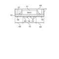
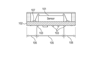
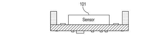
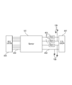
- FIG. 1 is a diagram schematically illustrating the configuration of an imaging unit according to an embodiment of the present invention.
- the sensor chip 101 is a sensor chip that outputs an image signal according to incident light.
- the sensor chip 101 is a semiconductor chip such as a CMOS image sensor formed on a silicon substrate.
- an image sensor made of a semiconductor other than a CCD sensor or silicon may be used.
- the present invention is suitable for the configuration of the sensor chip 101 having a large number of input / output signal lines, and is a laminate in which signal processing chips for performing signal processing are stacked on an imaging chip having a photoelectric conversion unit that converts light into electricity This is more suitable for a type image sensor.
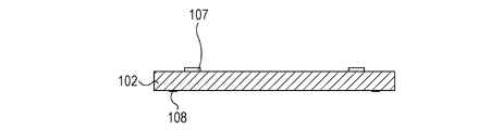
- the imaging board 102 is an imaging substrate.
- the imaging board 102 is a printed board, and components 103 and the like described later are arranged.
- each pattern on the imaging substrate 102 is formed of a metal having low electrical resistance such as gold or copper, and is electrically connected to the sensor chip 101 by wire bonding wiring using a gold wire or the like.
- the imaging substrate 102 is made of glass epoxy or the like because a rigid substrate is desirable in consideration of stability for mounting the sensor chip 101.
- the present invention is not limited to this, and may be a flexible substrate using a plastic material, an LTCC (low temperature co-fired ceramics) substrate using ceramics and copper wiring, or the like.
- any substrate may be used as long as a pattern can be formed on a specific material using a metal wiring such as copper and components can be mounted.
- a printed board is a board composed of a plurality of layers, and different materials may be used in combination as long as conduction is provided for each layer by vias or the like.
- the electronic component 103 is an electronic component.
- the electronic component 103 includes discrete components such as a capacitor, a resistor, and a coil necessary for operating the sensor chip 101.
- an IC chip such as a regulator for supplying power for operating the sensor chip 101 and an oscillator for supplying a clock signal is included. Further, it may include parts for other uses than operating the sensor chip 101 such as a thermometer for monitoring the state of the sensor chip 101 and a memory for storing solid information of the sensor chip 101.
- the electronic component 103 is mounted on the surface of the imaging substrate 102 opposite to the sensor chip 101. However, it is preferable that the noise removing capacitor or the like be closer to the connection terminal. You may make it mount on the same surface.
- the 104 is a connector having a plurality of electrical contacts.
- a board-to-board type (BtoB) connector for exchanging power and signals between the imaging substrate 102 and an external substrate including a signal processing chip that processes an imaging signal acquired from the sensor chip 101 In this part, various signals are connected together.
- the connector type may be a connector for connecting a flexible substrate.
- the connector 104 is mounted on the surface of the imaging substrate 102 opposite to the sensor chip 101. Further, when the number of terminals that need to be connected to the external substrate increases as the function of the sensor chip 101 increases, the size of the connector 104 also increases. In such a case, it is preferable to connect to an external board using a plurality of connectors 104.
- a range indicated by an arrow 105 on the image pickup substrate 102 is an area that is substantially coincident with the back surface portion of the sensor chip 101 and indicates a part area in which the part 103 and the connector 104 are arranged.
- a range indicated by an arrow 106 is a region around the component region 105 and indicates a prohibited region where the electronic component 103 and the connector 104 are not arranged.
- the imaging substrate 102 may be deformed by heat or the like, and it is preferable to mount the imaging substrate 102 near the back surface of the sensor chip 101 without mounting the electronic component 103 in the peripheral portion where the influence of the deformation is large.
- the component area 105 corresponds to a first area
- the prohibited area 106 corresponds to a second area.
- the component area 105 is larger than the back surface portion of the sensor chip 101.
- this is a configuration in which the number of parts 103 for driving the sensor chip 101 is large or the size is large.
- the component area 105 is further increased, and is an area larger than the area where the wire bonding pads 107 are disposed. Even in this case, it suffices if the wire bonding pad 107 can be heated and the imaging substrate 102 can be pressed at the time of manufacture.
- the component area 105 and the prohibited area 106 are determined according to the size of the sensor chip 101, the number of components 103, and the like.
- Reference numeral 107 denotes a wire bonding pad for connecting the sensor chip 101 and the imaging substrate 102 by wire bonding such as a gold wire. Specifically, it is an electrode formed on the surface of the imaging substrate 102 by a surface treatment such as gold plating.
- the wire bonding pad 107 is disposed on the same surface as the sensor chip 101 on the imaging substrate 102.
- Reference numeral 108 denotes a check pad (hereinafter, also referred to as CP), which is an electrode formed on the surface layer of the imaging substrate 102 by a process such as gold, copper, aluminum, or solder plating, like the wire bonding pad 107. .
- the CP 108 is arranged on the same surface as the connector 104 on the imaging substrate 102.
- a range indicated by an arrow 106 on the imaging substrate 102 is a heating region for contacting a heater or the like to heat the wire bonding pad 107 during wire bonding.
- the forbidden area 106 only needs to have an area necessary for the fixing presser or the like to come into contact therewith. Note that the larger the area of the forbidden area 106, the larger the outer shape of the imaging substrate 102, or the smaller the component area 105 in which components can be placed. Therefore, more specifically, a region that is inwardly about 1 mm to 8 mm from the outer periphery of the imaging substrate 102 is desirable.
- the component region 105 is preferably the same region as the outer periphery of the sensor chip 101 or a region of the outer periphery of the substrate that enters the inner side of the sensor chip 101 by about 0 mm to 5 mm.
- region 106 around 4 edges of the outer periphery of the imaging board
- it may be provided on one side or two sides along the outer periphery of the imaging substrate 102, and each area may be a different area as long as the fixing presser can be contacted. It may be different.
- a frame 110 is formed on the outer periphery of the wire bonding pad 107.
- the frame 110 is bonded to the imaging substrate 102 and the cover glass 109 to seal the sensor chip 101.
- the side surface of the frame 110 does not have to be perpendicular to the imaging substrate 102, and is formed with a predetermined inclination in order to suppress reflection of the side surface.
- the frame 110 is formed of a resin or the like, but may be formed of a ceramic material, a metal material, or a combination of these materials. Further, the frame 110 may have a shape having a fixing part such as a metal for fixing to the main body of the imaging apparatus described later.
- FIG. 3 is a diagram schematically showing a manufacturing flow of the imaging unit according to the embodiment of the present invention.
- FIG. 3A shows a state where only the imaging substrate 102 is present, and the component 103 and the like are not mounted.
- the imaging substrate 102 is assembled in a state in which a plurality of substrates are coupled and fixed to a predetermined jig such as a tray.
- the wire bonding pad 107 and the CP 108 are formed on the surface of the imaging substrate 102.
- a pattern for mounting the component 103 and a wiring for connecting the components are also formed.
- FIG. 3B shows a state in which the component 103 and the connector 104 are mounted on the imaging substrate 102.
- Each component is mounted on the imaging substrate 102 by a method such as a reflow process by applying cream solder or the like using a predetermined mask.
- the wire bonding pad 107 may be subjected to a surface treatment using a sputtering method or the like.
- FIG. 3C shows a state where the frame 110 is bonded to the imaging substrate 102. Adhesion is performed using a photocurable resin or the like as an adhesive, but is not limited thereto.
- FIG. 3D shows a state where the sensor chip 101 is mounted on the imaging substrate 102. The sensor chip 101 is fixed to the imaging substrate 102 with an adhesive (not shown).
- FIG. 3E shows a state where the sensor chip 101 and the wire bonding pad 107 are connected by wire bonding. In the wire bonding operation for connecting the sensor chip 101 and the imaging substrate 102, the sensor chip 101 and the imaging substrate 102 are heated on a heat stage in order to melt the metal used for wire bonding. Finally, in FIG. 3F, the image pickup unit is assembled by sealing the sensor chip 101 with the cover glass 109.
- the imaging unit in the present embodiment performs an inspection to confirm whether or not normal operation is possible (giving an electrically correct signal) to the imaging unit manufactured by the manufacturing flow shown in FIG.
- a power source and a clock are supplied to the sensor chip 101 to check whether a predetermined signal is output. If the expected signal is output, it is a non-defective product, and if it is not output, it is processed as a defective product.
- the operation of the sensor chip 101 mounted on the imaging unit of the present embodiment is confirmed even in the wafer state before assembly.
- the inspection contents in the wafer state are the same as those in the imaging unit described later. That is, the sensor chip 101 is inspected twice. As described with reference to FIG.
- the sensor chip 101 is heated at the time of wire bonding and further contacts various parts during the assembly process. In these series of operations, there is a possibility that the sensor chip 101 breaks down until the cover glass 109 is sealed. Therefore, it is necessary to inspect whether it operates normally after assembly.
- inspection before mounting is performed at the stage of a small package. Is possible.
- the inspection is performed for each printed board. In this case, since the inspection includes not only the sensor chip 101 but also the imaging substrate 102 and other electronic components, the size of the imaging unit may be relatively large, and a simple configuration in the inspection is essential. Become.
- FIG. 4 is a diagram schematically showing the signal relationship of the imaging unit according to the embodiment of the present invention.
- Reference numeral 401 denotes an input connector of the connector 104.
- the input connector 401 is a connector for connecting to an external substrate having a control unit that controls the sensor chip 101 to acquire an image, and a signal for driving the sensor chip 101 is connected thereto.
- the signals for driving the sensor chip 101 in this embodiment include a clock signal, a synchronization signal, a serial communication signal, a power supply, and the like.
- a signal input from the input connector 401 is input to the sensor chip 101 through the input wiring 402 wired on the imaging substrate 102.
- a part of the power supply circuit that drives the sensor chip 101 can supply stable power to the sensor chip 101 by arranging the linear regulator 403 or the like in the middle of the wiring 402. Note that the linear regulator 403 is not necessarily used, and power may be directly supplied via the input connector 401. Note that the number of signals connected to the input connector 401 is about ten.
- the output connector 405 is an output connector of the connector 104.
- the output connector 405 is a connector for connecting to an external substrate having a signal processing unit for generating image data from an output signal from the sensor chip 101, and is connected to a serial signal line for signal output.
- the output signal from the sensor chip 101 in the present embodiment includes not only the pixel signal from each pixel but also information (pixel address, pixel attribute, etc.) related to the output pixel signal, and includes a header or a footer, a synchronization code
- a clock signal for capturing an image signal is also included.
- the processing result may be output as an output signal.
- a signal output to the output connector 405 is output from the sensor chip 101 through the output wiring 404 wired on the imaging substrate 102. Since the signal from the sensor chip 101 is required to be transmitted at high speed, the output wiring 404 is a differential serial signal line conforming to the LVDS standard or the SLVS standard. The output of the sensor chip 101 is 20 channels, and 40 signal lines are wired on the imaging substrate 102 at an equal length.
- the CP 108 is connected to the input wiring 402 between the input connector 401 and the sensor chip 101 via a predetermined wiring. That is, it is possible to drive the sensor chip 101 via the CP 108 without connecting to an external substrate having a control unit at the input connector. Although details of control of the sensor chip 101 using the CP 108 will be described later, it is mainly used to perform an electrical inspection with the sensor chip 101 without going through the input connector 401 when inspecting the imaging unit.
- the CP 108 is preferably not connected to the differential pair wiring of the output wiring 404. This is because the output signal of the sensor chip 101 is a high-speed signal compared to the input signal. When the CP 108 is connected to the output wiring 404, it becomes a stub wiring, so that the signal quality of the output signal of the sensor chip 101 is lowered. This is to avoid this.
- CP 108 is also connected between the linear regulator 403 and the sensor chip 101.
- the linear regulator 403 is for supplying a voltage for normal operation of the sensor chip 101, it is necessary to adopt this configuration in order to perform inspection using other voltages. For example, it is possible to operate in a driving mode for inspection by applying a high voltage or a low voltage, and it is possible to perform inspection in an abnormal state by applying a reverse bias.
- FIG. 6 a signal relationship of the imaging unit according to the embodiment of the present invention, which is different from the configuration in FIG. 4 and FIG.
- a switch 601 that is a switch circuit is disposed between the linear regulator 403 and the sensor chip 101.
- various voltages can be applied from the CP 108 between the sensor chip 101 and the switch 601 from the outside.
- the voltage applied from the CP 108 to the sensor chip 101 can be set in a wide range without being restricted by the power supply voltage of the linear regulator 403 and the like.
- Signals and power for controlling the switch 601 can also be realized by inputting from the CP 108 or the like.
- the input signal of the sensor chip 101 is connected to the CP 108, and the output signal is not connected to the CP 108, so that the signal necessary for the inspection is maintained while maintaining the signal quality of the output signal. 101 can be input. In addition, it is possible to easily apply a power source necessary for the inspection of the sensor chip 101 from the outside.
- FIG. 7 is a diagram schematically illustrating a connection relationship during inspection and use of the imaging unit according to the embodiment of the present invention.
- FIG. 7A is a diagram for explaining the connection relationship at the time of inspection of the imaging unit.
- Reference numeral 701 denotes an interface board of the inspection apparatus, and inspection is performed by attaching an imaging unit to the board.
- the interface board 701 supplies a signal for driving the sensor chip 101 via the CP 108 and receives an output signal via the output connector 405.
- An inspection connector 702 is connected to the output connector 405.
- a normal BtoB connector is gripped to prevent it from falling off after being joined, but the interface board 701 uses a component that does not hold a dedicated gripper because a plurality of imaging units are repeatedly attached and detached.
- Reference numeral 703 denotes an inspection pin, which is connected to the CP 108 when the imaging unit is attached to the interface board 701.
- the inspection pin 703 is a contact that can be expanded and contracted, and by pressing the pin against the CP 108, it is possible to ensure good conduction.
- the inspection pin 703 is used for supplying a signal and power for driving the sensor
- FIG. 7B is a diagram for explaining the connection relationship during normal use of the imaging unit.
- “Normal use” means a case where it is mounted on an imaging device or the like described later and used for an operation for capturing a subject image through a lens.
- Reference numeral 704 denotes a first connector connected to the output connector 405, and reference numeral 705 denotes a second connector connected to the input connector.
- the imaging unit is incorporated in an imaging apparatus or the like, it is connected to another substrate through the first connector 704 and the second connector 705.
- the first connector 704 and the second connector 705 are mounted on a substrate (not shown), they are mounted on different substrates.
- the input connector 401 and the output connector 405 are precise electronic components, they always include dimensional errors in mass production.
- the first connector 704 and the second connector 705 are arranged on different substrates and connected to each other.
- it may be on the same substrate.
- the image pickup unit is attached to the inspection apparatus using an automatic transfer machine or the like in consideration of adhesion of dust and electrostatic breakdown.
- the first connector 704 and the second connector 705 are arranged on one board, but the fitting of both connectors is not guaranteed as described above. There's a problem.
- the inspection time is extended. That is, when a plurality of imaging units are to be inspected with one inspection apparatus, two connectors cannot be used and productivity is lowered.
- the output connector 405 is used at the time of inspection, and the input of the sensor chip 101 uses the CP 108 to secure the connection with a very simple conveyor even in the configuration having two or more connectors. be able to. As an effect, stable inspection can be performed with a short tact.
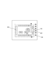
- FIG. 8 to 11 are diagrams schematically showing the layout of the imaging substrate according to the embodiment of the present invention.
- FIG. 8A shows the layout of the imaging substrate 102 on the surface (table) on which the sensor chip 101 is mounted.
- FIG. 8B shows the layout of the imaging substrate 102 on the surface (back) on which the component 103 is arranged.
- Reference numeral 801 denotes an area where the sensor chip 101 is disposed.
- the wire bonding pad 107 is disposed around the sensor chip 101.
- the input connector 401, the output connector 405, the component 103, and the like are disposed in the region of the component region 105 on the back surface where the components of the imaging substrate 102 are disposed.
- a region 106 extends from the component region 105 to the end of the imaging substrate 102.
- the sensor layout area 801 is actually the substrate surface on the surface where the parts are arranged. Does not exist.
- the component region 105 is described as a region smaller than the sensor chip 101, but is not limited to this configuration.
- the CP 108 is arranged in the area 106. Further, as shown in the figure, it is optimal to arrange on one or more sides according to the number of CPs 108. Furthermore, it is possible to increase the area for the CP 108 by arranging the CP 108 on the long side rather than the short side of the image sensor.
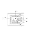
- FIG. 9 shows another example of the arrangement of the CP 108.
- the CP 108 is arranged on a side that is symmetric with respect to the arrangement direction of the output connector 405.
- FIG. 10 shows another example of the arrangement of the CP 108, and a part of the CP 108 is also arranged in the part area 105.
- a part of the CP 108 is also arranged in the part area 105.
- the CP 108 in the component region 105.
- the CP 108 is arranged in the component area, the area in which the component 103 can be arranged in the component area 105 is reduced. Therefore, even when the CP 108 is arranged in the component area, it is preferable that the number of the CP 108 in the area 106 is larger than that in the area 105 as shown in the figure.
- FIG. 11 shows another example of the arrangement of the CP 108, which is an example in which the CPs 108 are arranged in a plurality of rows or arranged in a staggered manner.
- the area of the region 106 increases and the area of the component region 105 may decrease, which is effective when the region 106 is sufficiently wide.
- the component region 105 be appropriately arranged, but also the region 106 can be secured in the peripheral portion of the substrate. Become.
- the CP 108 is not arranged on the output connector 405 through which the high-speed signal line passes, but the CP 108 is arranged only for the input signal, so that the inspection can be performed when there are two connectors, and the inspection is performed without reducing the output signal quality. Is possible. Further, it is possible to supply a voltage necessary for the inspection to the sensor chip 101 without being influenced by the voltage of the linear regulator.
- reference numeral 1201 denotes a lens unit that forms an optical image of a subject on the sensor chip 101.
- the lens driving device 1202 performs zoom control, focus control, aperture control, and the like.
- a mechanical shutter 1203 is controlled by the shutter control unit 1204.
- Reference numeral 101 denotes an image pickup device for capturing the subject imaged by the lens unit 1201 as an image signal
- 1206 denotes an image pickup signal processing for performing various corrections on the image signal output from the solid-state image pickup device 1205 and compressing data. Circuit.
- Reference numeral 1207 denotes a sensor chip 101, a timing generation circuit which is a driving means for outputting various timing signals to the imaging signal processing circuit 1206, 1209 denotes a control circuit which controls various operations and the entire imaging apparatus, and 1208 temporarily stores image data. It is a memory to do.
- Reference numeral 1210 denotes an interface for recording or reading on a recording medium
- 1211 denotes a removable recording medium such as a semiconductor memory for recording or reading image data
- 1212 denotes a display unit for displaying various information and photographed images. It is.
- Reference numeral 1213 denotes a photometric device that detects the brightness of a subject.
- Reference numeral 1214 denotes a distance measuring device for detecting focus.
- the sensor chip 101 is mounted on the imaging substrate 102, and the imaging substrate 102 is connected to a substrate on which the imaging signal processing circuit 1206 and the timing generation unit 1207 are mounted via a connector.
- the power supply for the control system is turned on, and the power supply for the image pickup system circuit such as the image pickup signal processing circuit 1206 is turned on.
- the lens unit is driven by the lens driving device 1202 to determine whether or not it is in focus. When it is determined that the lens unit is not in focus, the lens unit is driven again to perform distance measurement.
- the image signal output from the sensor chip 101 is subjected to signal processing by the imaging signal processing circuit 1206 and written to the memory 1208 by the control circuit 1209.
- Data stored in the memory 1208 is recorded on a removable recording medium 1211 such as a semiconductor memory through the recording medium control I / F unit 1210 under the control of the control circuit 1209.
- the image processing may be performed by directly inputting to a computer or the like through the external I / F unit 1210.
- the imaging unit and the imaging apparatus described in each embodiment can be applied to various applications.
- the imaging unit can be used for sensing light such as infrared light, ultraviolet light, and X-rays in addition to visible light.
- the imaging device is typified by a digital camera, but can also be applied to a camera-equipped mobile phone such as a smartphone, a surveillance camera, and a game machine.
- the present invention can be applied to endoscopes and medical devices that perform blood vessel imaging, beauty devices that observe skin and scalp, and video cameras that capture sports and action videos. It can also be applied to traffic purpose cameras such as traffic and ship monitoring and drive recorders, academic cameras such as astronomical observation and specimen observation, home appliances with cameras, machine vision and the like. In particular, machine vision is not limited to robots in factories and the like, and can be used in agriculture and fisheries.
- the configuration of the imaging apparatus shown in the above embodiment is an example, and the imaging apparatus to which the present invention can be applied is not limited to the configuration shown in FIG. Further, the circuit configuration of each part of the imaging apparatus is not limited to the configuration shown in each drawing.
- the present invention supplies a program that realizes one or more functions of the above-described embodiments to a system or apparatus via a network or a storage medium, and one or more processors in a computer of the system or apparatus read and execute the program
- This process can be realized. It can also be realized by a circuit (for example, ASIC) that realizes one or more functions.
Landscapes
- Solid State Image Pick-Up Elements (AREA)
- Structures For Mounting Electric Components On Printed Circuit Boards (AREA)
- Wire Bonding (AREA)
- Camera Bodies And Camera Details Or Accessories (AREA)
Abstract
Description
図1は、本発明の実施形態の撮像ユニットの構成を概略的に示す図である。
各実施形態で説明した撮像ユニットおよび撮像装置は様々なアプリケーションに適用可能である。例えば、撮像ユニットは可視光以外にも赤外光、紫外光、X線等の光のセンシングに用いることが可能である。また、撮像装置はデジタルカメラに代表されるが他にも、スマートフォン等のカメラ付携帯電話、監視カメラ、ゲーム機器等にも適用可能である。さらに、内視鏡や血管撮像を行う医療機器や、肌や頭皮を観察する美容機器、スポーツやアクション動画を撮像するためのビデオカメラに適用できる。そして、交通や船舶監視やドライブレコーダー等の交通目的カメラ、天体観測や検体観察等の学術用途カメラ、カメラ付き家電製品、マシンビジョン等にも適用可能である。特にマシンビジョンとして、工場等におけるロボットには限られず、農業や漁業での活用も可能である。
Claims (16)
- イメージセンサを構成する半導体チップと、前記半導体チップを実装する基板から成る撮像ユニットであって、
前記半導体チップを制御するための複数の入力配線と、
前記入力配線に接続する複数の第1の電極と、
前記入力配線に接続する入力コネクタとを備え、
前記基板は前記半導体チップを実装する反対の面において、電子部品を実装するための第1の領域と前記半導体チップの実装に用いる第2の領域とを含み、
前記コネクタは前記第1の領域に設けられ、前記第1の電極のうち少なくとも1以上は第2の領域に設けられることを特徴とする撮像ユニット。 - 前記半導体チップからの画像信号を出力するための出力配線に接続する出力コネクタをさらに備える請求項1に記載の撮像ユニット。
- 前記出力コネクタに接続する出力配線は高速信号を伝送するための差動対配線であることを特徴とする請求項2に記載の撮像ユニット。
- 前記入力コネクタまたは前記出力コネクタはボードトゥボード型のコネクタであることを特徴とする請求項2または3に記載の撮像ユニット。
- 前記基板は半導体チップを実装する面において前記半導体チップとワイヤボンディング接続を行うための第2の電極を備え、
前記第2の電極は、前記第2の領域に対応する反対の面に設けられることを特徴とする請求項1乃至4のいずれか1項に記載の撮像ユニット。 - 前記第1の領域は、前記半導体チップが実装されている領域を反対の面に対応させた領域と略一致することを特徴とする請求項1乃至5のいずれか1項に記載の撮像ユニット。
- 前記入力コネクタと前記半導体チップを接続する配線中に一つ以上の電源回路を備え、前記第1の電極は前記電源回路と前記半導体チップの間および前記電源回路と前記入力コネクタの間の配線に接続されることを特徴とする請求項1乃至6のいずれか1項に記載の撮像ユニット。
- 前記第1の電極が接続する前記電源回路と前記半導体チップの間の配線はスイッチ回路を備えることを特徴とする請求項7に記載の撮像ユニット。
- 前記第2の領域は前記基板の外周部に設けられていることを特徴とする請求項1乃至8のいずれか1項に記載の撮像ユニット。
- 前記第2領域は前記半導体チップのワイヤボンディング接続を行うための加熱領域であることを特徴とする請求項1乃至9のいずれか1項に記載の撮像ユニット。
- 前記第1の領域および前記第2の領域の夫々に第1の電極を備え、
前記第1の領域に備えられた前記第1の電極の数は前記第2の領域に備えられた前記第1の電極の数よりも少ないことを特徴とする請求項1乃至10のいずれか1項に記載の撮像ユニット。 - 前記第1の電極は、前記基板の周辺部の4辺のうちの2辺に配置されることを特徴とする請求項1から請求項11のいずれか1項に記載の撮像装置。
- 前記第1の電極は、前記基板の周辺部の4辺のうちの長い辺に配置されることを特徴とする請求項1から請求項11のいずれか1項に記載の撮像装置。
- イメージセンサを構成する半導体チップと、前記半導体チップを実装する基板から成る撮像ユニットの製造方法であって、
前記半導体チップを制御するための複数の入力配線に対して接続する、複数の第1の電極を基板外周部に設けるステップと、
前記半導体チップを制御するための複数の入力配線に対して接続する、入力コネクタを設けるステップと、
電子部品を前記基板における第1の領域に実装するためステップと、
前記第1の領域と異なり前記第1の電極が設けられた第2の領域を用いて前記半導体チップを実装するステップとを含むことを特徴とする撮像ユニットの製造方法。 - 前記半導体チップが実装された基板をカバーガラスで封止するステップと、
前記カバーガラスで封止された状態で前記半導体チップを検査する検査ステップとを更に含み、
前記検査ステップは前記第1の電極を用いて前記半導体チップを制御することを特徴とする請求項14に記載の撮像ユニットの製造方法。 - イメージセンサを構成する半導体チップと、前記半導体チップを実装する基板と、
前記半導体チップを制御するための複数の入力配線と、
前記入力配線に接続する複数の第1の電極と、
前記入力配線に接続する入力コネクタとを備え、
前記基板は前記半導体チップを実装する反対の面において、電子部品を実装するための第1の領域と前記半導体チップの実装に用いる第2の領域とを含み、
前記コネクタは前記第1の領域に設けられ、前記第1の電極のうち少なくとも1以上は第2の領域に設けられる撮像ユニットを備えることを特徴とする撮像装置。
Priority Applications (4)
| Application Number | Priority Date | Filing Date | Title |
|---|---|---|---|
| EP19793883.0A EP3787023B1 (en) | 2018-04-27 | 2019-04-19 | Imaging unit and method for manufacturing same |
| CN201980039653.1A CN112368833B (zh) | 2018-04-27 | 2019-04-19 | 图像拍摄单元及其制造方法和图像拍摄装置 |
| BR112020021559-7A BR112020021559B1 (pt) | 2018-04-27 | 2019-04-19 | Unidade de captura de imagem e método para a fabricação da mesma |
| US17/075,536 US11990495B2 (en) | 2018-04-27 | 2020-10-20 | Image capturing unit and method for manufacturing the same |
Applications Claiming Priority (2)
| Application Number | Priority Date | Filing Date | Title |
|---|---|---|---|
| JP2018-087519 | 2018-04-27 | ||
| JP2018087519A JP7171223B2 (ja) | 2018-04-27 | 2018-04-27 | 撮像ユニットおよびその製造方法 |
Related Child Applications (1)
| Application Number | Title | Priority Date | Filing Date |
|---|---|---|---|
| US17/075,536 Continuation US11990495B2 (en) | 2018-04-27 | 2020-10-20 | Image capturing unit and method for manufacturing the same |
Publications (1)
| Publication Number | Publication Date |
|---|---|
| WO2019208415A1 true WO2019208415A1 (ja) | 2019-10-31 |
Family
ID=68294859
Family Applications (1)
| Application Number | Title | Priority Date | Filing Date |
|---|---|---|---|
| PCT/JP2019/016760 Ceased WO2019208415A1 (ja) | 2018-04-27 | 2019-04-19 | 撮像ユニットおよびその製造方法 |
Country Status (5)
| Country | Link |
|---|---|
| US (1) | US11990495B2 (ja) |
| EP (1) | EP3787023B1 (ja) |
| JP (2) | JP7171223B2 (ja) |
| CN (1) | CN112368833B (ja) |
| WO (1) | WO2019208415A1 (ja) |
Families Citing this family (4)
| Publication number | Priority date | Publication date | Assignee | Title |
|---|---|---|---|---|
| US11817397B2 (en) * | 2020-12-21 | 2023-11-14 | Advanced Semiconductor Engineering, Inc. | Semiconductor device package |
| CN114497018A (zh) * | 2022-01-24 | 2022-05-13 | 西安微电子技术研究所 | 一种多腔体图像采集处理微系统模块及制作方法 |
| KR20240158688A (ko) * | 2023-04-27 | 2024-11-05 | 엘지이노텍 주식회사 | 이미지 센서 모듈, 카메라 모듈 및 그 제조방법 |
| WO2025253958A1 (ja) * | 2024-06-04 | 2025-12-11 | ソニーセミコンダクタソリューションズ株式会社 | 半導体装置 |
Citations (6)
| Publication number | Priority date | Publication date | Assignee | Title |
|---|---|---|---|---|
| JPH03241842A (ja) * | 1990-02-20 | 1991-10-29 | Fujitsu Ltd | 回路基板の加熱方法 |
| JP2005268602A (ja) * | 2004-03-19 | 2005-09-29 | Mitsubishi Electric Corp | 位相配線構造 |
| JP2015012211A (ja) | 2013-07-01 | 2015-01-19 | 株式会社ニコン | 撮像ユニット及び撮像装置 |
| WO2015099140A1 (ja) * | 2013-12-27 | 2015-07-02 | 株式会社ニコン | 撮像ユニット及び撮像装置 |
| JP2017037204A (ja) * | 2015-08-11 | 2017-02-16 | キヤノン株式会社 | 電子部品実装部への異物混入を防止する構成を有する電子機器 |
| JP2018087519A (ja) | 2016-11-29 | 2018-06-07 | 株式会社ヴァレオジャパン | スクロール型圧縮機 |
Family Cites Families (9)
| Publication number | Priority date | Publication date | Assignee | Title |
|---|---|---|---|---|
| JP3507251B2 (ja) * | 1995-09-01 | 2004-03-15 | キヤノン株式会社 | 光センサicパッケージおよびその組立方法 |
| JP4139051B2 (ja) * | 2000-06-28 | 2008-08-27 | 富士フイルム株式会社 | リニアイメージセンサチップおよびリニアイメージセンサ |
| KR101070921B1 (ko) * | 2006-10-19 | 2011-10-06 | 삼성테크윈 주식회사 | 이미지 센서용 칩 패키지 및 그 제조방법 |
| JP4384198B2 (ja) * | 2007-04-03 | 2009-12-16 | シャープ株式会社 | 固体撮像装置およびその製造方法、電子情報機器 |
| JP5269157B2 (ja) | 2011-07-22 | 2013-08-21 | キヤノン株式会社 | 撮像装置 |
| JP5844580B2 (ja) * | 2011-09-05 | 2016-01-20 | 浜松ホトニクス株式会社 | 固体撮像素子及び固体撮像素子の実装構造 |
| CN105657296B (zh) * | 2014-10-11 | 2019-12-24 | 意法半导体有限公司 | 具有互连层间隙的图像感测设备及相关方法 |
| EP3410691A4 (en) | 2016-01-28 | 2019-08-14 | Olympus Corporation | IMAGING UNIT, IMAGE MODULE AND ENDOSCOPE |
| JP6780277B2 (ja) | 2016-03-29 | 2020-11-04 | 株式会社ニコン | 基板 |
-
2018
- 2018-04-27 JP JP2018087519A patent/JP7171223B2/ja active Active
-
2019
- 2019-04-19 CN CN201980039653.1A patent/CN112368833B/zh active Active
- 2019-04-19 EP EP19793883.0A patent/EP3787023B1/en active Active
- 2019-04-19 WO PCT/JP2019/016760 patent/WO2019208415A1/ja not_active Ceased
-
2020
- 2020-10-20 US US17/075,536 patent/US11990495B2/en active Active
-
2022
- 2022-11-02 JP JP2022175968A patent/JP7418095B2/ja active Active
Patent Citations (6)
| Publication number | Priority date | Publication date | Assignee | Title |
|---|---|---|---|---|
| JPH03241842A (ja) * | 1990-02-20 | 1991-10-29 | Fujitsu Ltd | 回路基板の加熱方法 |
| JP2005268602A (ja) * | 2004-03-19 | 2005-09-29 | Mitsubishi Electric Corp | 位相配線構造 |
| JP2015012211A (ja) | 2013-07-01 | 2015-01-19 | 株式会社ニコン | 撮像ユニット及び撮像装置 |
| WO2015099140A1 (ja) * | 2013-12-27 | 2015-07-02 | 株式会社ニコン | 撮像ユニット及び撮像装置 |
| JP2017037204A (ja) * | 2015-08-11 | 2017-02-16 | キヤノン株式会社 | 電子部品実装部への異物混入を防止する構成を有する電子機器 |
| JP2018087519A (ja) | 2016-11-29 | 2018-06-07 | 株式会社ヴァレオジャパン | スクロール型圧縮機 |
Also Published As
| Publication number | Publication date |
|---|---|
| JP2022190051A (ja) | 2022-12-22 |
| JP7171223B2 (ja) | 2022-11-15 |
| EP3787023B1 (en) | 2025-08-27 |
| US20210036044A1 (en) | 2021-02-04 |
| EP3787023A4 (en) | 2022-03-09 |
| US11990495B2 (en) | 2024-05-21 |
| BR112020021559A2 (pt) | 2021-01-19 |
| CN112368833B (zh) | 2024-05-17 |
| JP2019192884A (ja) | 2019-10-31 |
| JP7418095B2 (ja) | 2024-01-19 |
| CN112368833A (zh) | 2021-02-12 |
| EP3787023A1 (en) | 2021-03-03 |
Similar Documents
| Publication | Publication Date | Title |
|---|---|---|
| JP7418095B2 (ja) | 撮像ユニットおよびその製造方法 | |
| US11309299B2 (en) | Image sensor package and endoscope | |
| US11728447B2 (en) | Semiconductor device and imaging apparatus | |
| US8823872B2 (en) | Image pickup module with improved flatness of image sensor and via electrodes | |
| US10074757B2 (en) | Semiconductor package, sensor module, and production method | |
| KR20100022327A (ko) | 카메라 모듈 패키지 및 그 공정 방법 | |
| JPWO2008132980A1 (ja) | 撮像装置の製造方法、撮像装置及び携帯端末 | |
| WO2012173014A1 (ja) | 撮像装置及びこれを用いた電子機器 | |
| TWI746620B (zh) | 相機模組、製造方法及電子機器 | |
| WO2020062140A1 (zh) | 芯片封装结构、方法和电子设备 | |
| JP6990317B2 (ja) | 撮像ユニット及び撮像装置 | |
| CN205726035U (zh) | 影像模组结构 | |
| JP6757862B2 (ja) | 撮像ユニット及び撮像装置 | |
| CN104603946A (zh) | 拍摄单元、拍摄装置、及拍摄单元的制造方法 | |
| TWI543613B (zh) | 影像感測模組 | |
| JP2002329849A (ja) | 撮像装置 | |
| JPWO2019163909A1 (ja) | 撮像ユニット、撮像装置 | |
| WO2024009694A1 (ja) | 半導体装置、電子機器および半導体装置の製造方法 | |
| BR112020021559B1 (pt) | Unidade de captura de imagem e método para a fabricação da mesma | |
| JP2002334976A (ja) | 半導体装置の製造方法 | |
| JP2006245359A (ja) | 光電変換装置及びその製造方法 | |
| JP6777118B2 (ja) | 撮像ユニット及び撮像装置 | |
| JPH1033475A (ja) | 内視鏡用撮像ユニット | |
| JP2024074533A (ja) | 電子部品および機器 | |
| JPH04117940A (ja) | 電子内視鏡撮像装置 |
Legal Events
| Date | Code | Title | Description |
|---|---|---|---|
| 121 | Ep: the epo has been informed by wipo that ep was designated in this application |
Ref document number: 19793883 Country of ref document: EP Kind code of ref document: A1 |
|
| NENP | Non-entry into the national phase |
Ref country code: DE |
|
| REG | Reference to national code |
Ref country code: BR Ref legal event code: B01A Ref document number: 112020021559 Country of ref document: BR |
|
| WWE | Wipo information: entry into national phase |
Ref document number: 2019793883 Country of ref document: EP |
|
| ENP | Entry into the national phase |
Ref document number: 112020021559 Country of ref document: BR Kind code of ref document: A2 Effective date: 20201021 |
|
| WWG | Wipo information: grant in national office |
Ref document number: 2019793883 Country of ref document: EP |