WO2019218559A1 - 有机电致发光装置 - Google Patents
有机电致发光装置 Download PDFInfo
- Publication number
- WO2019218559A1 WO2019218559A1 PCT/CN2018/106347 CN2018106347W WO2019218559A1 WO 2019218559 A1 WO2019218559 A1 WO 2019218559A1 CN 2018106347 W CN2018106347 W CN 2018106347W WO 2019218559 A1 WO2019218559 A1 WO 2019218559A1
- Authority
- WO
- WIPO (PCT)
- Prior art keywords
- layer
- light emitting
- organic
- light
- organic light
- Prior art date
- Legal status (The legal status is an assumption and is not a legal conclusion. Google has not performed a legal analysis and makes no representation as to the accuracy of the status listed.)
- Ceased
Links
Images




Classifications
-
- H—ELECTRICITY
- H10—SEMICONDUCTOR DEVICES; ELECTRIC SOLID-STATE DEVICES NOT OTHERWISE PROVIDED FOR
- H10K—ORGANIC ELECTRIC SOLID-STATE DEVICES
- H10K59/00—Integrated devices, or assemblies of multiple devices, comprising at least one organic light-emitting element covered by group H10K50/00
- H10K59/30—Devices specially adapted for multicolour light emission
- H10K59/35—Devices specially adapted for multicolour light emission comprising red-green-blue [RGB] subpixels
- H10K59/351—Devices specially adapted for multicolour light emission comprising red-green-blue [RGB] subpixels comprising more than three subpixels, e.g. red-green-blue-white [RGBW]
-
- C—CHEMISTRY; METALLURGY
- C09—DYES; PAINTS; POLISHES; NATURAL RESINS; ADHESIVES; COMPOSITIONS NOT OTHERWISE PROVIDED FOR; APPLICATIONS OF MATERIALS NOT OTHERWISE PROVIDED FOR
- C09K—MATERIALS FOR MISCELLANEOUS APPLICATIONS, NOT PROVIDED FOR ELSEWHERE
- C09K11/00—Luminescent materials, e.g. electroluminescent or chemiluminescent
- C09K11/08—Luminescent materials, e.g. electroluminescent or chemiluminescent containing inorganic luminescent materials
- C09K11/70—Luminescent materials, e.g. electroluminescent or chemiluminescent containing inorganic luminescent materials containing phosphorus
-
- H—ELECTRICITY
- H10—SEMICONDUCTOR DEVICES; ELECTRIC SOLID-STATE DEVICES NOT OTHERWISE PROVIDED FOR
- H10K—ORGANIC ELECTRIC SOLID-STATE DEVICES
- H10K50/00—Organic light-emitting devices
- H10K50/10—OLEDs or polymer light-emitting diodes [PLED]
- H10K50/11—OLEDs or polymer light-emitting diodes [PLED] characterised by the electroluminescent [EL] layers
-
- H—ELECTRICITY
- H10—SEMICONDUCTOR DEVICES; ELECTRIC SOLID-STATE DEVICES NOT OTHERWISE PROVIDED FOR
- H10K—ORGANIC ELECTRIC SOLID-STATE DEVICES
- H10K50/00—Organic light-emitting devices
- H10K50/10—OLEDs or polymer light-emitting diodes [PLED]
- H10K50/11—OLEDs or polymer light-emitting diodes [PLED] characterised by the electroluminescent [EL] layers
- H10K50/125—OLEDs or polymer light-emitting diodes [PLED] characterised by the electroluminescent [EL] layers specially adapted for multicolour light emission, e.g. for emitting white light
-
- H—ELECTRICITY
- H10—SEMICONDUCTOR DEVICES; ELECTRIC SOLID-STATE DEVICES NOT OTHERWISE PROVIDED FOR
- H10K—ORGANIC ELECTRIC SOLID-STATE DEVICES
- H10K50/00—Organic light-emitting devices
- H10K50/10—OLEDs or polymer light-emitting diodes [PLED]
- H10K50/11—OLEDs or polymer light-emitting diodes [PLED] characterised by the electroluminescent [EL] layers
- H10K50/125—OLEDs or polymer light-emitting diodes [PLED] characterised by the electroluminescent [EL] layers specially adapted for multicolour light emission, e.g. for emitting white light
- H10K50/13—OLEDs or polymer light-emitting diodes [PLED] characterised by the electroluminescent [EL] layers specially adapted for multicolour light emission, e.g. for emitting white light comprising stacked EL layers within one EL unit
- H10K50/131—OLEDs or polymer light-emitting diodes [PLED] characterised by the electroluminescent [EL] layers specially adapted for multicolour light emission, e.g. for emitting white light comprising stacked EL layers within one EL unit with spacer layers between the electroluminescent layers
-
- H—ELECTRICITY
- H10—SEMICONDUCTOR DEVICES; ELECTRIC SOLID-STATE DEVICES NOT OTHERWISE PROVIDED FOR
- H10K—ORGANIC ELECTRIC SOLID-STATE DEVICES
- H10K50/00—Organic light-emitting devices
- H10K50/10—OLEDs or polymer light-emitting diodes [PLED]
- H10K50/19—Tandem OLEDs
-
- H—ELECTRICITY
- H10—SEMICONDUCTOR DEVICES; ELECTRIC SOLID-STATE DEVICES NOT OTHERWISE PROVIDED FOR
- H10K—ORGANIC ELECTRIC SOLID-STATE DEVICES
- H10K50/00—Organic light-emitting devices
- H10K50/80—Constructional details
- H10K50/805—Electrodes
- H10K50/81—Anodes
- H10K50/818—Reflective anodes, e.g. ITO combined with thick metallic layers
-
- H—ELECTRICITY
- H10—SEMICONDUCTOR DEVICES; ELECTRIC SOLID-STATE DEVICES NOT OTHERWISE PROVIDED FOR
- H10K—ORGANIC ELECTRIC SOLID-STATE DEVICES
- H10K50/00—Organic light-emitting devices
- H10K50/80—Constructional details
- H10K50/805—Electrodes
- H10K50/82—Cathodes
-
- H—ELECTRICITY
- H10—SEMICONDUCTOR DEVICES; ELECTRIC SOLID-STATE DEVICES NOT OTHERWISE PROVIDED FOR
- H10K—ORGANIC ELECTRIC SOLID-STATE DEVICES
- H10K50/00—Organic light-emitting devices
- H10K50/80—Constructional details
- H10K50/805—Electrodes
- H10K50/82—Cathodes
- H10K50/828—Transparent cathodes, e.g. comprising thin metal layers
-
- H—ELECTRICITY
- H10—SEMICONDUCTOR DEVICES; ELECTRIC SOLID-STATE DEVICES NOT OTHERWISE PROVIDED FOR
- H10K—ORGANIC ELECTRIC SOLID-STATE DEVICES
- H10K50/00—Organic light-emitting devices
- H10K50/80—Constructional details
- H10K50/85—Arrangements for extracting light from the devices
- H10K50/852—Arrangements for extracting light from the devices comprising a resonant cavity structure, e.g. Bragg reflector pair
-
- H—ELECTRICITY
- H10—SEMICONDUCTOR DEVICES; ELECTRIC SOLID-STATE DEVICES NOT OTHERWISE PROVIDED FOR
- H10K—ORGANIC ELECTRIC SOLID-STATE DEVICES
- H10K59/00—Integrated devices, or assemblies of multiple devices, comprising at least one organic light-emitting element covered by group H10K50/00
- H10K59/30—Devices specially adapted for multicolour light emission
-
- H—ELECTRICITY
- H10—SEMICONDUCTOR DEVICES; ELECTRIC SOLID-STATE DEVICES NOT OTHERWISE PROVIDED FOR
- H10K—ORGANIC ELECTRIC SOLID-STATE DEVICES
- H10K59/00—Integrated devices, or assemblies of multiple devices, comprising at least one organic light-emitting element covered by group H10K50/00
- H10K59/30—Devices specially adapted for multicolour light emission
- H10K59/35—Devices specially adapted for multicolour light emission comprising red-green-blue [RGB] subpixels
-
- H—ELECTRICITY
- H10—SEMICONDUCTOR DEVICES; ELECTRIC SOLID-STATE DEVICES NOT OTHERWISE PROVIDED FOR
- H10K—ORGANIC ELECTRIC SOLID-STATE DEVICES
- H10K59/00—Integrated devices, or assemblies of multiple devices, comprising at least one organic light-emitting element covered by group H10K50/00
- H10K59/30—Devices specially adapted for multicolour light emission
- H10K59/38—Devices specially adapted for multicolour light emission comprising colour filters or colour changing media [CCM]
-
- H—ELECTRICITY
- H10—SEMICONDUCTOR DEVICES; ELECTRIC SOLID-STATE DEVICES NOT OTHERWISE PROVIDED FOR
- H10K—ORGANIC ELECTRIC SOLID-STATE DEVICES
- H10K59/00—Integrated devices, or assemblies of multiple devices, comprising at least one organic light-emitting element covered by group H10K50/00
- H10K59/80—Constructional details
- H10K59/805—Electrodes
- H10K59/8051—Anodes
- H10K59/80518—Reflective anodes, e.g. ITO combined with thick metallic layers
-
- H—ELECTRICITY
- H10—SEMICONDUCTOR DEVICES; ELECTRIC SOLID-STATE DEVICES NOT OTHERWISE PROVIDED FOR
- H10K—ORGANIC ELECTRIC SOLID-STATE DEVICES
- H10K59/00—Integrated devices, or assemblies of multiple devices, comprising at least one organic light-emitting element covered by group H10K50/00
- H10K59/80—Constructional details
- H10K59/875—Arrangements for extracting light from the devices
- H10K59/876—Arrangements for extracting light from the devices comprising a resonant cavity structure, e.g. Bragg reflector pair
-
- H—ELECTRICITY
- H10—SEMICONDUCTOR DEVICES; ELECTRIC SOLID-STATE DEVICES NOT OTHERWISE PROVIDED FOR
- H10K—ORGANIC ELECTRIC SOLID-STATE DEVICES
- H10K77/00—Constructional details of devices covered by this subclass and not covered by groups H10K10/80, H10K30/80, H10K50/80 or H10K59/80
- H10K77/10—Substrates, e.g. flexible substrates
- H10K77/111—Flexible substrates
-
- H—ELECTRICITY
- H10—SEMICONDUCTOR DEVICES; ELECTRIC SOLID-STATE DEVICES NOT OTHERWISE PROVIDED FOR
- H10K—ORGANIC ELECTRIC SOLID-STATE DEVICES
- H10K85/00—Organic materials used in the body or electrodes of devices covered by this subclass
- H10K85/30—Coordination compounds
- H10K85/321—Metal complexes comprising a group IIIA element, e.g. Tris (8-hydroxyquinoline) gallium [Gaq3]
- H10K85/324—Metal complexes comprising a group IIIA element, e.g. Tris (8-hydroxyquinoline) gallium [Gaq3] comprising aluminium, e.g. Alq3
-
- H—ELECTRICITY
- H10—SEMICONDUCTOR DEVICES; ELECTRIC SOLID-STATE DEVICES NOT OTHERWISE PROVIDED FOR
- H10K—ORGANIC ELECTRIC SOLID-STATE DEVICES
- H10K85/00—Organic materials used in the body or electrodes of devices covered by this subclass
- H10K85/60—Organic compounds having low molecular weight
- H10K85/649—Aromatic compounds comprising a hetero atom
- H10K85/653—Aromatic compounds comprising a hetero atom comprising only oxygen as heteroatom
-
- H—ELECTRICITY
- H10—SEMICONDUCTOR DEVICES; ELECTRIC SOLID-STATE DEVICES NOT OTHERWISE PROVIDED FOR
- H10K—ORGANIC ELECTRIC SOLID-STATE DEVICES
- H10K85/00—Organic materials used in the body or electrodes of devices covered by this subclass
- H10K85/60—Organic compounds having low molecular weight
- H10K85/649—Aromatic compounds comprising a hetero atom
- H10K85/657—Polycyclic condensed heteroaromatic hydrocarbons
- H10K85/6572—Polycyclic condensed heteroaromatic hydrocarbons comprising only nitrogen in the heteroaromatic polycondensed ring system, e.g. phenanthroline or carbazole
-
- H—ELECTRICITY
- H10—SEMICONDUCTOR DEVICES; ELECTRIC SOLID-STATE DEVICES NOT OTHERWISE PROVIDED FOR
- H10K—ORGANIC ELECTRIC SOLID-STATE DEVICES
- H10K85/00—Organic materials used in the body or electrodes of devices covered by this subclass
- H10K85/60—Organic compounds having low molecular weight
- H10K85/649—Aromatic compounds comprising a hetero atom
- H10K85/657—Polycyclic condensed heteroaromatic hydrocarbons
- H10K85/6574—Polycyclic condensed heteroaromatic hydrocarbons comprising only oxygen in the heteroaromatic polycondensed ring system, e.g. cumarine dyes
-
- H—ELECTRICITY
- H10—SEMICONDUCTOR DEVICES; ELECTRIC SOLID-STATE DEVICES NOT OTHERWISE PROVIDED FOR
- H10K—ORGANIC ELECTRIC SOLID-STATE DEVICES
- H10K2102/00—Constructional details relating to the organic devices covered by this subclass
- H10K2102/10—Transparent electrodes, e.g. using graphene
- H10K2102/101—Transparent electrodes, e.g. using graphene comprising transparent conductive oxides [TCO]
-
- H—ELECTRICITY
- H10—SEMICONDUCTOR DEVICES; ELECTRIC SOLID-STATE DEVICES NOT OTHERWISE PROVIDED FOR
- H10K—ORGANIC ELECTRIC SOLID-STATE DEVICES
- H10K2102/00—Constructional details relating to the organic devices covered by this subclass
- H10K2102/10—Transparent electrodes, e.g. using graphene
- H10K2102/101—Transparent electrodes, e.g. using graphene comprising transparent conductive oxides [TCO]
- H10K2102/103—Transparent electrodes, e.g. using graphene comprising transparent conductive oxides [TCO] comprising indium oxides, e.g. ITO
-
- H—ELECTRICITY
- H10—SEMICONDUCTOR DEVICES; ELECTRIC SOLID-STATE DEVICES NOT OTHERWISE PROVIDED FOR
- H10K—ORGANIC ELECTRIC SOLID-STATE DEVICES
- H10K2102/00—Constructional details relating to the organic devices covered by this subclass
- H10K2102/301—Details of OLEDs
- H10K2102/351—Thickness
Definitions
- the present application relates to the field of display technologies, and in particular, to an organic electroluminescent device.
- OLED Organic Light Emitting Display
- OLED is an active light emitting display device with high contrast, wide viewing angle, low power consumption, thinner volume, etc., and can be printed by inkjet printing technology and volume. It is easy to realize flexible display by roll to roll process, and it is one of the most concerned technologies in flat panel display technology.
- color gamut is a method of encoding a color, and also refers to the sum of colors that a technical system can produce.
- 1 is a color coordinate map developed by the National Television Standards Committee (NTSC). As can be seen from the figure, the larger the color gamut area, the richer the display color of the display device, and the better the viewing experience.
- the color gamut area is generally improved by increasing the purity of the three primary colors.
- the first, synthetic narrow-spectrum luminescent material uses a narrow-spectrum luminescent material to improve the purity of the luminescent color of the pixel;
- the quantum dot is introduced, and the narrow spectral characteristic of the quantum dot is used to improve the color purity.
- the above solutions have their own drawbacks.
- the synthesis workload is large, the yield is low, and a large amount of experimental verification is required, and the research and development cost is high;
- the introduction of the quantum dot technology can improve the color gamut, it is substantially photoluminescence, not electroluminescence, and the luminous efficiency is low.
- the method also improves the process complexity, and it is difficult to realize high-density pixel arrangement. .
- the technical problem to be solved by the present application is the problem that the color gamut of the OLED device is not high enough in the prior art.
- the present application provides an organic electroluminescent device comprising m light emitting units having different light emitting wavelengths, the light emitting unit being an organic light emitting diode, the organic light emitting diode comprising a monochromatic light organic light emitting diode and/or being provided with a filter White light organic light emitting diode of light sheet;
- At least one of the organic light emitting diodes has a microcavity structure
- microcavity optical path L i of the organic light emitting diode having the microcavity structure and the corresponding emission wavelength ⁇ i of the light emitting unit satisfy the following relationship:
- n i ⁇ 2 n i is a positive integer, and at least one of the m types of light-emitting units having different light-emitting wavelengths ⁇ i corresponds to n i greater than or equal to 3; m ⁇ i ⁇ 1, i, m are positive Integer.
- n is 3, ⁇ 1 > ⁇ 2 > ⁇ 3 ; and n 2 > n 1 , n 2 > n 3 .
- the organic light emitting diode comprises a first electrode layer, a light emitting layer and a second electrode layer which are sequentially stacked, and the microcavity structure is formed between the first electrode layer and the second electrode layer.
- the thickness H i of the light-emitting layer in each of the organic light-emitting diodes having different light-emitting wavelengths satisfies the following relationship: H 2 >H 1 , H 2 >H 3 .
- At least one of the organic light emitting diodes has at least two of the light emitting layers; and a connecting layer is further disposed between the adjacent light emitting layers.
- the connecting layer is a transparent layer, and a single film formed of one material selected from the group consisting of Li 2 CO 3 , HAT-CN, TAPC, TACG and HAT-CN doping materials, Ag, ITO, and the like.
- a multilayer laminated composite structure formed of layers or materials.
- the connecting layer has a thickness of 5 nm to 100 nm.
- the connecting layer has a refractive index of 1.6-2.2.
- a heat activated delayed fluorescent material is included in the light emitting layer of at least one of the organic light emitting diodes.
- the luminescent layer comprises a host material and a guest material, the host material comprising at least one thermally activated delayed fluorescent material, the guest material being a fluorescent material.
- the host material comprises two thermally activated delayed fluorescent materials, the two thermally activated delayed fluorescent materials forming an exciplex.
- the thermally activated delayed fluorescent material is selected from the group consisting of 4CzIPN, 2CzPN, 4CzPN, 4CzTPN, 4CzTPN-Me, 4CzTPN-Ph, and the fluorescent material is selected from the group consisting of Alq3, C545T, DPVBi, DCJTB.
- a light compensation layer is further disposed in the microcavity structure of the at least one of the organic light emitting diodes.
- the light compensation layer is at least one of a hole injection layer, a hole transport layer, an electron blocking layer, a hole blocking layer, an electron transport layer, and an electron injection layer.
- the first electrode layer of the at least one of the organic light emitting diodes is a reflective electrode layer
- the second electrode layer is a semi-transflective electrode layer
- the thicknesses of the reflective electrode layers in each of the organic light emitting diodes having different light emitting wavelengths are not all the same.
- the reflective electrode layer comprises a reflective layer and an anode layer disposed in a stack; the thickness of the anode layer in each of the organic light emitting diodes having different light emitting wavelengths is not the same, and the reflective layer has the same thickness.
- the reflective layer is a layer of metallic material and the anode layer is a high work function layer.
- the reflective layer is a metallic silver layer and the anode layer is an ITO layer.
- the transflective electrode layer comprises at least two layers of metal oxide layers and/or metal layers which are sequentially stacked.
- the metal oxide layer is selected from the group consisting of MoO 3 , WO 3 , and IZO, and the metal layer is selected from the group consisting of Ag and Mg.
- the transflective electrode layer has a light transmittance of not less than 15%.
- the semi-transflective electrode layer has a refractive index greater than 1 and less than 2.
- the organic electroluminescent device provided by the embodiment of the present application includes m kinds of light-emitting units having different light-emitting wavelengths, that is, light of m different light-emitting wavelengths are mixed together to realize full-color display.
- the light emitting unit is a monochromatic light organic light emitting diode and/or a white light organic light emitting diode provided with a filter, that is, a plurality of monochromatic light organic light emitting diodes having different light emitting wavelengths can be combined to realize full color display.
- microcavity optical path L i and the illuminating wavelength ⁇ i of each of the above m kinds of organic light emitting diodes having different illuminating wavelengths having a microcavity structure satisfy the following relationship:
- n i ⁇ 2 n i is a positive integer, and at least one of the m types of light-emitting units having different light-emitting wavelengths ⁇ i corresponds to n i greater than or equal to 3; m ⁇ i ⁇ 1, i, m are positive Integer.
- the optical path of the microcavity is of the same order of magnitude as the wavelength of the light
- the light of a specific wavelength is selected and strengthened to achieve a narrowing of the spectrum, that is, a microcavity effect is generated.
- the microcavity optical path L i of the organic light emitting diode having the microcavity structure in the organic electroluminescent device provided by the embodiment of the present application is n i times of the corresponding emission wavelength, that is, in the organic light emitting diode having the microcavity structure
- n i is a positive integer greater than or equal to 2, so that a second-order microcavity, a third-order microcavity, a fourth-order microcavity or a higher-order microcavity can be realized, and the microcavity effect is enhanced.
- the spectrum is further narrowed, thereby increasing the color gamut area.
- the organic electroluminescent device provided by the embodiment of the present application m is 3, ⁇ 1 > ⁇ 2 > ⁇ 3 , that is, the organic electroluminescent device includes an organic light emitting diode having three kinds of light emitting wavelengths, and the three wavelengths are respectively It has monochromaticity, for example, ⁇ 1 is the red wavelength, ⁇ 2 is the green wavelength, and ⁇ 3 is the blue wavelength, and the full color display is realized by the conventional three primary colors.
- n 2 >n 1 , n 2 >n 3 that is, the intensity of the microcavity effect of the organic light emitting diode corresponding to the green light is greater than the intensity of the microcavity effect of the organic light emitting diode corresponding to the red light and the blue light.
- the red light device can realize the color gamut expansion by spectral red shift, and the green light device is difficult to be like red light due to its own limitations.
- the device realizes the expansion of the color gamut like the blue light device. Therefore, the embodiment of the present application focuses on enhancing the microcavity effect of the green light device to match the high color gamut of the red light device and the blue light device, thereby realizing the entire organic electroluminescent device. High color gamut.
- Embodiment of the present application provides an organic electroluminescent device, 577nm ⁇ 2 ⁇ 492nm, n 2 ⁇ 3 , i.e. the number of order of a green wavelength microcavity organic light emitting diode is 3 or higher order, by increasing the green The microcavity intensity of an organic light emitting diode expands its color gamut area.
- the organic electroluminescent device provided by the embodiment of the present application includes the first electrode layer, the light emitting layer and the second electrode layer which are sequentially stacked, since the first electrode layer and the second electrode layer have corresponding transmission or The reflection property, the microcavity structure can be formed between the first electrode layer and the second electrode layer, thereby increasing the color gamut area by enhancing the microcavity effect.
- the thickness H i of the light-emitting layer in each of the organic light-emitting diodes having different emission wavelengths satisfies the following relationship: H 2 >H 1 , H 2 >H 3 . That is, the thickness of the light-emitting layer of the organic light-emitting diode corresponding to the green light-emitting wavelength is adjusted to be larger than the thickness of the light-emitting layer of the organic light-emitting diode corresponding to the red light-emitting wavelength and greater than the thickness of the light-emitting layer of the organic light-emitting diode corresponding to the blue light-emitting wavelength.
- the adjustment of the thickness of the light-emitting layer realizes the adjustment of the microcavity order, that is, the intensity of the microcavity, and increases the color gamut area of the organic light-emitting diode corresponding to the green light-emitting wavelength, thereby ensuring a high color gamut of the entire organic electroluminescent device.
- the organic electroluminescent device provided by the embodiment of the present application, at least one of the organic light emitting diodes has at least two light emitting layers.
- the microcavity length can be increased by increasing the number of the light emitting layers, thereby increasing the microcavity light. Cheng, improve the strength of the microcavity.
- the luminous flux can be effectively increased, and the luminous efficiency of the organic light emitting diode can be improved.
- At least one of the light emitting layers of the organic light emitting diode includes a thermally activated delayed fluorescent (TADF) material, and a thermal activation delay is added to the light emitting layer relative to the conventional light emitting layer material.
- TADF thermally activated delayed fluorescent
- Fluorescent materials help achieve higher luminous efficiency while ensuring higher color purity.
- At least one of the microcavity structures of the organic light emitting diode is further provided with a light compensation layer.
- the setting of the optical compensation layer helps to increase the length of the microcavity in the corresponding organic light emitting diode, that is, the optical path of the microcavity is increased, thereby increasing the order of the microcavity and enhancing the microcavity effect, thereby realizing the narrowing and color gamut of the chromatogram. The expansion of the area.
- the optical compensation layer is at least one of a hole injection layer, a hole transport layer, an electron blocking layer, a hole blocking layer, an electron transport layer, and an electron injection layer.
- the thicknesses of the reflective electrode layers in the respective organic light emitting diodes having different emission wavelengths are not the same, and the thickness may be set according to different properties of the emitted light (eg, wavelength, spectrum, etc.).
- the reflective electrode layer further adjusts the optical path of the emitted light in the microcavity, thereby realizing different microcavity strengths of different emitting organic light emitting diodes, and ensuring a high color gamut and a narrow spectrum of the organic electroluminescent device as a whole.
- the reflective electrode layer includes a reflective layer and an anode layer which are stacked.
- the reflective layer and the anode layer together form a reflective electrode layer, which increases the thickness of the reflective electrode layer and increases the optical path, thereby enhancing the microcavity effect; on the other hand, the arrangement of the reflective layer improves the reflection effect of the reflective electrode layer. The microcavity effect is further enhanced.
- the transflective electrode layer includes at least two layers of metal oxide layers and/or metal layers which are sequentially stacked, thereby providing a plurality of metal oxides and/or Or the metal layer increases the thickness of the transflective electrode layer, increases the optical path of the microcavity, thereby enhancing the microcavity effect; and, since the transmissivity of the transflective electrode layer is not less than 15%, sufficient Light output efficiency.
- Figure 1 is a prior art NTSC color gamut
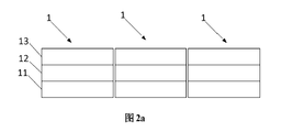
- FIG. 2a is a schematic structural view of an embodiment of an organic electroluminescent device according to an embodiment of the present application
- FIG. 2b is a schematic structural diagram of an embodiment of an organic electroluminescent device according to an embodiment of the present application.
- FIG. 3 is a schematic structural view of an embodiment of an organic electroluminescent device according to an embodiment of the present application.
- FIG. 4 is a schematic structural diagram of an embodiment of an organic electroluminescent device according to an embodiment of the present application.
- FIG. 5 is a schematic structural diagram of an embodiment of an organic electroluminescent device according to an embodiment of the present application.
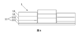
- FIG. 6 is a schematic structural diagram of an embodiment of an organic electroluminescent device according to an embodiment of the present application.
- FIG. 7 is a schematic structural diagram of an embodiment of an organic electroluminescent device according to an embodiment of the present application.
- 1-organic light-emitting diode 11-first electrode layer; 111-reflective layer; 112-anode layer; 12-light-emitting layer; 121-connection layer; 13-second electrode layer; 131-metal oxide layer; Layer; 14-filter; 15-light compensation layer; 151-hole injection layer; 152-hole transport layer; 153-electron barrier layer; 154-hole blocking layer; 155-electron transport layer; Inject the layer.
- An embodiment of the present application provides an organic electroluminescent device, including m kinds of light emitting units having different light emitting wavelengths, and the light emitting unit is an organic light emitting diode 1 , and the organic light emitting diode 1 includes a monochromatic light organic light emitting diode 1 and/or
- the white organic light-emitting diode 1 provided with the filter 14 is a red filter or a green light filter or a blue light filter, depending on the wavelength of the light to be emitted.
- the structure in which the light-emitting unit is the monochromatic light-emitting diode 1 is shown in Fig. 2a; the structure in which the light-emitting unit is the white-light organic light-emitting diode 1 provided with the filter 14 is shown in Fig. 2b.
- At least one of the above-described organic light emitting diodes 1 has a microcavity structure.
- microcavity optical path L i of each of the above m kinds of organic light emitting diodes 1 having different emission wavelengths having a microcavity structure and the corresponding emission wavelength ⁇ i of the corresponding light emitting unit satisfy the following relationship:
- n i ⁇ 2 n i is a positive integer, and at least one of the m kinds of light-emitting units having different light-emitting wavelengths ⁇ i corresponds to n i greater than or equal to 3; m ⁇ i ⁇ 1, i, m are positive integers .
- the organic electroluminescent device provided by the embodiment of the present application includes m light emitting units of different light emitting wavelengths, that is, light of m kinds of light emitting wavelengths are mixed together to realize full color display.
- a monochromatic light organic light emitting diode with different light emitting wavelengths or a white light organic light emitting diode provided with a color filter that is, a combination of a plurality of monochromatic light organic light emitting diodes having different light emitting wavelengths, can realize full color display.
- a combination of a red organic light emitting diode, a green organic light emitting diode, and a blue organic light emitting diode realizes a full color display; or a combination of a plurality of white organic light emitting diodes, which filter out light of different wavelengths through a filter, such as filtering Red light, green light, and blue light are mixed to form a full color display; or a monochromatic light organic light emitting diode and a white light organic light emitting diode with different light emitting wavelengths may be combined to form a full color display. Therefore, it is applicable to different kinds of organic light emitting diodes, and has a wide application range.
- microcavity optical path L i and the illuminating wavelength ⁇ i of each of the above m kinds of organic light emitting diodes having different illuminating wavelengths having a microcavity structure satisfy the following relationship:
- n i ⁇ 2 n i is a positive integer
- at least one of the above m kinds of light-emitting units having different light-emitting wavelengths ⁇ i corresponds to n i is greater than or equal to 3
- m ⁇ i ⁇ 1 m are positive integers.
- the optical path of the microcavity is of the same order of magnitude as the wavelength of the light
- the light of a specific wavelength is selected and strengthened to achieve a narrowing of the spectrum, that is, a microcavity effect is generated.
- the microcavity optical path L i of the organic light emitting diode having the microcavity structure in the organic electroluminescent device provided by the embodiment of the present application is n i times of the corresponding emission wavelength, that is, in the organic light emitting diode having the microcavity structure
- n i is a positive integer greater than or equal to 2, so that a second-order microcavity, a third-order microcavity, a fourth-order microcavity or a higher-order microcavity can be realized, and the microcavity effect is enhanced.
- the spectrum is further narrowed, thereby increasing the color gamut area.
- n i is not all the same, that is, the order of the microcavity effect in each organic light emitting diode, that is, the intensity is not the same, and the order of different microcavity effects can be set according to different properties of the emitted light (eg, wavelength, spectrum, etc.). , in order to achieve the best spectral narrowing effect and the best color gamut area.
- m is 3, ⁇ 1 > ⁇ 2 > ⁇ 3 ; and n 2 > n 1 , n 2 > n 3 .
- the organic electroluminescence device includes emitted light of three wavelengths, and each of the three wavelengths has monochromaticity.
- ⁇ 1 is a red light wavelength
- a wavelength range is 600 nm to 760 nm
- ⁇ 2 is a green light wavelength
- a wavelength range is 492 nm to 577 nm
- ⁇ 3 is a blue light wavelength
- a wavelength range is 435 to 480 nm.
- the number of the organic light emitting diodes 1 is generally three, corresponding to the outgoing light of the above three wavelengths; the number of the organic light emitting diodes 1 may also be greater than or less than three, and the arrangement may be according to actual needs. And set, no specific restrictions here.
- n 2 >n 1 , n 2 >n 3 that is, the intensity of the microcavity effect of the organic light emitting diode 1 corresponding to the green light emitting wavelength is greater than the intensity of the microcavity effect of the organic light emitting diode 1 corresponding to the red light emitting wavelength
- the intensity of the microcavity effect of the organic light emitting diode 1 corresponding to the blue light emitting wavelength is larger, because the color coordinates of the blue light device itself are closer to the blue color coordinate of the high color gamut standard, and the red light device can realize the color gamut by spectral red shifting.
- the embodiment of the present application focuses on enhancing the microcavity effect of the green light device to match the red light device and The high color gamut of the blue light device is matched to achieve a high color gamut of the entire organic electroluminescent device.
- the microcavity order of the organic light emitting diode corresponding to the green light emitting wavelength may be set to 3, and the microcavity order of the organic light emitting diode corresponding to the red light emitting wavelength and the blue light emitting wavelength may be set to 2
- the microcavity order of the organic light emitting diode corresponding to the green light emitting wavelength may be set to 4th order
- the microcavity order of the organic light emitting diode corresponding to the red light emitting wavelength is set to 3rd order
- the microcavity order of the diode is set to 2 orders. Specifically, it can be set according to actual needs, and there is no excessive limit here.
- the microcavity order of the organic light emitting diode corresponding to the green light wavelength is 3rd order or higher, which significantly enhances the microcavity intensity of the green organic light emitting diode and expands its color gamut area.
- the organic light emitting diode 1 includes a first electrode layer 11 , a light emitting layer 12 , and a second electrode layer 13 , which are sequentially stacked, and a micro cavity is formed between the first electrode layer 11 and the second electrode layer 13 . structure.
- the microcavity optical path L specifically refers to a path in which the light emitted from the luminescent layer is reflected by the first electrode layer, reflected by the second electrode layer, returned to the starting position, and the first electrode layer and the second electrode.
- the microcavity structure can be formed between the first electrode layer and the second electrode layer, thereby increasing the color gamut area by enhancing the microcavity effect.
- the light emitting layer 12 is a monochromatic light emitting layer, such as a red light emitting layer or a blue light emitting layer or a green light emitting layer.
- the organic light emitting diode 1 is provided with the filter 14
- the white light organic light emitting diode the light emitting layer is generally a laminated structure of three red, green and blue light emitting layers, and the light emitting layer 12 emits white light, and the color filter 14 is separately filtered by the filter 14 respectively disposed thereon to realize color. Glowing.
- the thickness H i of the light-emitting layer 12 in each of the organic light-emitting diodes 1 having different light-emitting wavelengths satisfies the following relationship: H 2 >H 1 , H 2 >H 3 . That is, the thickness of the light-emitting layer of the organic light-emitting diode 1 corresponding to the green light-emitting wavelength is adjusted to be larger than the thickness of the light-emitting layer of the organic light-emitting diode 1 corresponding to the red light-emitting wavelength and also larger than the light-emitting layer 1 corresponding to the blue light-emitting wavelength. The thickness of the luminescent layer.
- the adjustment of the thickness of the light-emitting layer realizes the adjustment of the microcavity order, that is, the intensity of the microcavity, and increases the color gamut area of the organic light-emitting diode corresponding to the green light-emitting wavelength, thereby ensuring a high color gamut of the entire organic electroluminescent device.
- At least one organic light emitting diode 1 has at least two light emitting layers 12; and a connecting layer 121 is further disposed between adjacent light emitting layers 12.
- the microcavity length can be increased by increasing the number of luminescent layers, thereby increasing the microcavity optical path and increasing the microcavity intensity.
- the luminous flux can be effectively increased, and the luminous efficiency of the organic light emitting diode can be improved.
- the number of the light-emitting layers in the organic light-emitting diode corresponding to the green light-emitting wavelength is set to two, and the number of the light-emitting layers in the organic light-emitting diodes corresponding to the red light and blue light-emitting wavelengths is set to one.
- connection layer 121 connecting the adjacent light-emitting layers 12 is a transparent layer selected from, but not limited to, Li 2 CO 3 , 2, 3 , 6, 7, 10, 11-hexacyano-1, 4 , 5 , 8 , and 9. 12-hexaazatriphenylene (HAT-CN), 1,1-bis[4-(n,n'-bis(p-tolyl)amino]phenyl]cyclohexane (TAPC), TAPC and HAT-
- the film layer formed by one of CN doping materials (TAPC: HAT-CN), Ag, ITO, etc. may also be a multilayer laminated composite structure, for example, Li 2 CO 3 /HAT-CN stacked /TAPC, etc.
- the transparent connecting layer 121 has a thickness of 5 nm to 100 nm; and the refractive index is generally 1.6 to 2.2.
- the luminescent layer 12 of the at least one organic light emitting diode 1 comprises a thermally activated delayed fluorescent (TADF) material.
- TADF thermally activated delayed fluorescent
- the addition of a thermally activated delayed fluorescent (TADF) material to the luminescent layer helps achieve higher luminous efficiency relative to conventional luminescent layer materials while ensuring higher color purity.
- a thermally activated delayed fluorescent material may be added to the luminescent layer corresponding to the red light emitting wavelength, or a thermally activated delayed fluorescent material may be added to the luminescent layer corresponding to the green light emitting wavelength, and the corresponding luminescent light may be emitted at a blue light emitting wavelength.
- a thermally activated delayed fluorescent material is added to the layer.
- the luminescent layer includes a host material and a guest material, and the host material includes at least one thermally activated delayed fluorescent material, and the guest material is a fluorescent material.
- the embodiment of the present application adds a heat-activated delayed fluorescent material to the host material, and uses the fluorescent material as a guest material to thermally activate the delayed fluorescent material at room temperature. It is possible to convert the triplet excitons which cannot be illuminated into single-link excitons which can be utilized, thereby improving the luminous efficiency.
- the organic electroluminescent device can be ensured to have a narrow spectrum, a high color purity, and a high color gamut area.
- the host material comprises two thermally activated delayed fluorescent materials, and the two thermally activated delayed fluorescent materials form an exciplex.
- the luminous efficiency of the organic light emitting diode can be further improved.
- the fluorescent material is used as a guest in the light-emitting layer. Therefore, according to the direct trapping light-emitting mechanism, a large number of triplet excitons cannot be effectively utilized for the guest fluorescent material, and the present embodiment uses two kinds of heat-activated delayed fluorescence.
- the material acts as a host material, and both can form an exciplex, thereby suppressing the trapping luminescence mechanism of the guest, improving the energy transfer efficiency, and further improving the luminescence efficiency.
- the thermally activated delayed fluorescent material may be selected from, but not limited to, 2,4,5,6-tetrakis(9-carbazolyl)-isophthalonitrile (4CzIPN), 4,5-di(9-carbazolyl).
- the fluorescent material is selected from the group consisting of not limited to tris(8-hydroxyquinoline)aluminum (Alq3), incense Beans 545T (C545T), 4,4'-bis(2,2-distyryl)-1,1'-biphenyl (DPVBi), 4-(dicyanovinyl)-2-tert-butyl- 6-(1,
- a light compensation layer 15 is further disposed in the microcavity structure of the at least one organic light emitting diode 1. Only the structure of one organic light emitting diode is shown in FIG.
- the setting of the optical compensation layer helps to increase the length of the microcavity in the corresponding organic light emitting diode, that is, the optical path of the microcavity is increased, thereby increasing the order of the microcavity and enhancing the microcavity effect, thereby realizing the narrowing and color gamut of the chromatogram. The expansion of the area.
- the light compensation layer 15 is a hole injection layer 151, a hole transport layer 152, an electron blocking layer 153, a hole blocking layer 154, an electron transport layer 155, and an electron injection layer. At least one of 156.
- the carrier transmission efficiency is improved, and the luminous efficiency of the organic light emitting diode is improved.
- one or two or more layers can be set according to actual needs, which is flexible and selective.
- the first electrode layer 11 is an anode and the second electrode layer 13 is a cathode
- a hole injection layer 151, a hole transport layer 152, and an electron blocking layer 153 are disposed between the first electrode layer 11 and the light emitting layer 12.
- Any one or more layers of the hole blocking layer 154, the electron transport layer 155, and the electron injection layer 156 are disposed between the light emitting layer 12 and the second electrode layer 13.
- the microcavity length can be further adjusted by adjusting the thickness of the hole transport layer, because the thickness of the hole transport layer has little influence on the electrical performance of the organic light emitting diode, and the microcavity intensity is adjusted. At the same time, it also guarantees good electrical performance.
- the first electrode layer 11 is a reflective electrode layer
- the second electrode layer 13 is a semi-transflective electrode layer. That is, a microcavity structure is formed between the first electrode layer and the second electrode layer by utilizing the reflection characteristics of the first electrode layer and the semi-transverse semi-transmissive property of the second electrode layer.
- the thicknesses of the reflective electrode layers in the respective organic light emitting diodes 1 of different emission wavelengths are not all the same.
- the reflectors of different thicknesses can be set according to different properties of the emitted light (for example, wavelength, spectrum, etc.), thereby adjusting the optical path of the emitted light in the microcavity, thereby realizing different micro-emitting diodes for different outgoing light.
- the cavity strength ensures a high color gamut and a narrow spectrum of the organic electroluminescent device as a whole.
- the reflective electrode layer includes a reflective layer 111 and an anode layer 112 which are stacked.
- the reflective layer 111 and the anode layer 112 together constitute a reflective electrode layer, on the one hand, the thickness of the reflective electrode layer is increased, the optical path is increased, and the microcavity effect is enhanced; on the other hand, the arrangement of the reflective layer 111 improves the reflective electrode layer. The reflection effect further enhances the microcavity effect.
- the thicknesses of the anode layers 112 in the respective organic light emitting diodes 1 of different emission wavelengths are not all the same, and the thickness of the reflective layer 111 is the same.
- the thickness of the anode layer of the organic light emitting diode corresponding to the green light emitting wavelength is set to be larger than the thickness of the anode layer of the organic light emitting diode corresponding to the red and blue light emitting wavelengths, and the thickness corresponding to the light emitting wavelength is adjusted by adjusting the thickness of the anode layer. The adjustment of the cavity length.
- the reflective layer 111 may be a metal material layer such as a metallic silver layer or the like.
- the anode layer 112 can be a high work function layer, such as an indium tin oxide (ITO) layer.
- ITO indium tin oxide
- the transflective electrode layer includes at least two layers of metal oxide layers and/or metal layers which are sequentially stacked.
- the semi-transflective electrode layer may include a metal oxide layer 131 and a metal layer 132 which are sequentially stacked, and may also include two metal oxide layers 131 which are sequentially stacked; or may be stacked in sequence
- a layer of metal oxide layer 131, a layer of metal layer 132 and a layer of metal oxide layer 131 may also be in other combinations, which may be set according to actual needs.
- the thickness of the transflective electrode layer is increased, and the microcavity optical path is increased, thereby enhancing the microcavity effect.
- the metal oxide layer 131 may be MoO 3 or WO 3 or indium zinc oxide (IZO) or the like; the metal layer 132 may be Ag or Mg or the like.
- the transflective electrode layer has a light transmittance of not less than 15% and a refractive index of more than 1 and less than 2.
- the embodiment of the present application provides a specific example of an organic electroluminescence device.
- the organic electroluminescent device in this embodiment includes three kinds of monochromatic light organic light emitting diodes having different light emitting wavelengths, namely a red organic light emitting diode, a green organic light emitting diode, and a blue organic light emitting diode. Among them, all three organic light emitting diodes have a microcavity structure. The light transmittance of the second electrode layer was 35%.
- the device structure of the red organic light emitting diode in this embodiment is: ITO (10 nm) / Ag (100 nm) / ITO (10 nm) / CuPc (20 nm) / TPD (200 nm) / CBP: Ir (piq) 3 (3%, 30 nm) / TPBi (40 nm) / LiF (1 nm) / Mg: Ag (20%, 15 nm) / NPB (60 nm).
- the device structure of the green organic light emitting diode in this embodiment is: ITO (10 nm) / Ag (100 nm) / ITO (10 nm) / CuPc (20 nm) / TPD (280 nm) / CBP: Ir (ppy) 3 (10%) , 30 nm) / TPBi (40 nm) / LiF (1 nm) / Mg: Ag (20%, 15 nm) / NPB (60 nm).
- the device structure of the blue organic light emitting diode in this embodiment is: ITO (10 nm) / Ag (100 nm) / ITO (10 nm) / CuPc (20 nm) / TPD (110 nm) / CBP: DPVBi (3%, 30 nm) / TPBi ( 40 nm) / LiF (1 nm) / Mg: Ag (20%, 15 nm) / NPB (60 nm).
- the thickness of the hole transport layer TPD of the green organic light emitting diode is greater than the thickness of the hole transport layer TPD of the red and blue organic light emitting diodes.
- the embodiment of the present application provides a specific example of an organic electroluminescence device.
- the difference from the organic electroluminescent device provided in Embodiment 1 is that the number of the light-emitting layers of the green light-emitting diode is two, and a connection layer is disposed between the two light-emitting layers.
- the device structure of the green organic light emitting diode is: ITO (10 nm) / Ag (100 nm) / ITO (10 nm) / CuPc (20 nm) / TPD (90 nm) / CBP: Ir (ppy) 3 (10%) , 30 nm) / TPBi (40 nm) / Li 2 CO 3 (1 nm) / HAT - CN (10 nm) / CuPc (20 nm) / TPD (90 nm) / CBP: Ir (ppy) 3 (3%, 30 nm) / TPBi ( 40 nm) / LiF (1 nm) / Mg: Ag (20%, 15 nm) / NPB (60 nm).
- the embodiment of the present application provides a specific example of an organic electroluminescence device.
- the difference from the organic electroluminescent device provided in Embodiment 1 is that the light-emitting layer of the green organic light emitting diode contains a thermally activated delayed fluorescent (TADF) material.
- TADF thermally activated delayed fluorescent
- the device structure of the green organic light emitting diode is: ITO (10 nm) / Ag (100 nm) / ITO (10 nm) / CuPc (20 nm) / TPD (280 nm) / 4 CzIPN: Ir (ppy) 3 (10%) (30 nm) / TPBi (40 nm) / LiF (1 nm) / Mg: Ag (20%, 15 nm) / NPB (60 nm).
- the embodiment of the present application provides a specific example of an organic electroluminescence device.
- the difference from the organic electroluminescent device provided in Embodiment 1 is that:
- the anode layer in the first electrode of the green organic light emitting diode is an optical compensation layer.
- the device structure of the green organic light emitting diode in this embodiment is: ITO (10 nm) / Ag (100 nm) / ITO (180 nm) / CuPc (20 nm) / TPD (100 nm) / CBP: Ir (ppy) 3 (10%, 30 nm) / TPBi (40 nm) / LiF (1 nm) / Mg: Ag (20%, 15 nm) / NPB (60 nm)
- the embodiment of the present application provides a specific example of an organic electroluminescence device.
- the difference from the organic electroluminescent device provided in Embodiment 1 is that:
- the second electrode layer of the organic light emitting diode having a green light emitting wavelength includes three metal oxide layers and a metal layer which are sequentially stacked.
- the device structure of the green organic light emitting diode in this embodiment is: ITO (10 nm) / Ag (100 nm) / ITO (10 nm) / CuPc (20 nm) / TPD (280 nm) / CBP: Ir (ppy) 3 (10%, 30 nm) / TPBi (40 nm) / LiF (1 nm) / Mg: Ag (20%, 10 nm) / MoO 3 (60 nm) / Mg: Ag (20%, 10 nm) / MoO 3 (60 nm)
- the embodiment of the present application provides a specific example of an organic electroluminescence device.
- the structure is the same as in the first embodiment, wherein the second electrode layer is Mg: Ag has a thickness of 25 nm and a light transmittance of 15%.
- the embodiment of the present application provides a specific example of an organic electroluminescence device.
- the difference from the organic electroluminescent device provided in Embodiment 1 is that:
- the device structure of the red organic light emitting diode in this embodiment is: ITO (10 nm) / Ag (100 nm) / ITO (10 nm) / CuPc (20 nm) / TPD (380 nm) / CBP: Ir (piq) 3 (3%, 30 nm) / TPBi (40 nm) / LiF (1 nm) / Mg: Ag (20%, 15 nm) / NPB (60 nm).
- the device structure of the green organic light emitting diode in this embodiment is: ITO (10 nm) / Ag (100 nm) / ITO (10 nm) / CuPc (20 nm) / TPD (430 nm) / CBP: Ir (ppy) 3 (10%, 30 nm) / TPBi (40 nm) / LiF (1 nm) / Mg: Ag (20%, 15 nm) / NPB (60 nm).
- the device structure of the blue organic light emitting diode in this embodiment is: ITO (10 nm) / Ag (100 nm) / ITO (10 nm) / CuPc (20 nm) / TPD (110 nm) / CBP: DPVBi (3%, 30 nm) / TPBi ( 40 nm) / LiF (1 nm) / Mg: Ag (20%, 15 nm) / NPB (60 nm).
- the embodiment of the present application provides a specific example of an organic electroluminescence device.
- the device structure is the same as in Embodiment 1.
- the organic electroluminescent device in this embodiment is composed of a white organic light emitting diode, and a red light filter, a green light filter and a blue light filter are respectively disposed on the light emitting surface of the white light organic light emitting diode.
- the device structure of the white organic light emitting diode is:
- Red light unit ITO (10 nm) / Ag (100 nm) / ITO (100 nm) / CuPc (20 nm) / TPD (20 nm) / CBP: Ir (ppy) 3 (15%): Ir (piq) 3 (0.2%) (30 nm) / TPBi (30 nm) / Li 2 CO 3 (1 nm) / HAT - CN (10 nm) / CuPc (20 nm) / TPD (20 nm) / CBP: DPVBi (3%, 30 nm) / TPBi (30 nm) / LiF (1 nm) /Mg: Ag (20%, 15 nm) / NPB (60 nm);
- Green light unit ITO (10 nm) / Ag (100 nm) / ITO (180 nm) / CuPc (20 nm) / TPD (20 nm) / CBP: Ir (ppy) 3 (15%): Ir (piq) 3 (0.2%) (30 nm) / TPBi (30 nm) / Li 2 CO 3 (1 nm) / HAT - CN (10 nm) / CuPc (20 nm) / TPD (20 nm) / CBP: DPVBi (3%, 30 nm) / TPBi (30 nm) / LiF (1 nm) /Mg: Ag (20%, 15 nm) / NPB (60 nm);
- the wavelengths of the red light filter, the green light filter, and the blue light filter are: 630 nm, 522 nm, and 456 nm, respectively.
- the embodiment of the present application provides a specific example of an organic electroluminescence device.
- the device structure is the same as in Embodiment 1.
- the difference from the organic electroluminescent device provided in Embodiment 1 is that:
- Red and blue organic light emitting diodes do not have a microcavity structure.
- the device structure of the red organic light emitting diode in this embodiment is: ITO (10 nm) / Ag (100 nm) / ITO (10 nm) / CuPc (20 nm) / TPD (200 nm) / CBP: Ir (piq) 3 (3%, 30 nm) / TPBi (40 nm) / LiF (1 nm) / Mg: Ag (20%, 15 nm) / NPB (60 nm).
- the device structure of the green organic light emitting diode in this embodiment is: ITO (10 nm) / Ag (100 nm) / ITO (10 nm) / CuPc (20 nm) / TPD (130 nm) / CBP: Ir (ppy) 3 (10%, 30 nm) / TPBi (40 nm) / LiF (1 nm) / Mg: Ag (20%, 15 nm) / NPB (60 nm).
- the device structure of the blue organic light emitting diode in this embodiment is: ITO (10 nm) / Ag (100 nm) / ITO (10 nm) / CuPc (20 nm) / TPD (110 nm) / CBP: DPVBi (3%, 30 nm) / TPBi ( 40 nm) / LiF (1 nm) / Mg: Ag (20%, 15 nm) / NPB (60 nm).
- the device structure of the red organic light emitting diode in this embodiment is: ITO (10 nm) / Ag (100 nm) / ITO (10 nm) / CuPc (20 nm) / TPD (20 nm) / CBP: Ir (piq) 3 (3%, 30 nm) / TPBi (40 nm) / LiF (1 nm) / Mg: Ag (20%, 15 nm) / NPB (60 nm);
- the device structure of the green organic light emitting diode in this embodiment is: ITO (10 nm) / Ag (100 nm) / ITO (10 nm) / CuPc (20 nm) / TPD (20 nm) / CBP: Ir (ppy) 3 (10%, 30 nm) / TPBi (20 nm) / LiF (1 nm) / Mg: Ag (20%, 15 nm) / NPB (60 nm);
- the device structure of the blue organic light emitting diode in this embodiment is: ITO (10 nm) / Ag (100 nm) / ITO (10 nm) / CuPc (10 nm) / TPD (20 nm) / CBP: DPVBi (3%, 20 nm) / TPBi ( 20 nm) / LiF (1 nm) / Mg: Ag (20%, 15 nm) / NPB (60 nm).
- This comparative example provides a specific example of an organic electroluminescence device.
- the device structure is the same as that of Embodiment 1, except that the second electrode layer is Mg: Ag has a thickness of 40 nm and a light transmittance of 10%.
- the embodiment of the present application can significantly improve the color purity and the color gamut area by adjusting the microcavity optical path, and the optimized color gamut area is close to 100% BT.2020. Maintain high device efficiency.
Landscapes
- Physics & Mathematics (AREA)
- Optics & Photonics (AREA)
- Chemical & Material Sciences (AREA)
- Engineering & Computer Science (AREA)
- Materials Engineering (AREA)
- Spectroscopy & Molecular Physics (AREA)
- Inorganic Chemistry (AREA)
- Organic Chemistry (AREA)
- Electroluminescent Light Sources (AREA)
Abstract
一种有机电致发光装置涉及显示技术领域。所述有机电致发光装置包括m种具有不同发光波长的发光单元,所述发光单元为有机发光二极管(1),所述有机发光二极管(1)包括单色光有机发光二极管(1)和/或设置有滤光片(14)的白光有机发光二极管(1);至少一种所述有机发光二极管(1)具有微腔结构;具有所述微腔结构的所述有机发光二极管(1)的微腔光程Li与所对应的所述发光单元的发光波长λi满足以下关系式:Li=niλi。其中,ni≥2,ni为正整数,所述m种具有不同发光波长λi的发光单元中的至少一种对应的ni大于等于3;m≥i≥1,i、m为正整数。即在具有微腔结构的有机发光二极管(1)中均可实现ni阶微腔效应,且ni为大于等于2的正整数,即可实现二阶微腔、三阶微腔、四阶微腔或更高阶微腔,增强了微腔效应,进一步窄化了光谱,进而提高了色域面积。
Description
本申请涉及显示技术领域,具体涉及一种有机电致发光装置。
有机电致发光显示器(英文全称Organic Light Emitting Display,简称OLED)是主动发光显示装置,由于其具有高对比度、广视角、低功耗、体积更薄等优点,而且可通过喷墨打印技术和卷对卷(roll to roll)工艺制备,易于实现柔性显示,是目前平板显示技术中受到关注最多的技术之一。
随着OLED技术的不断发展,对显示器件性能提出了越来越高的要求。例如,提高色域等。所谓色域是对一种颜色进行编码的方法,也指一个技术系统能够产生的颜色的总和。图1是NTSC(National Television Standards Committee(美国)国家电视标准委员会)制定的色坐标图,从图中可以看出,色域面积越大,显示装置的显示色彩越丰富,观看体验越好。
为了适应时代的发展趋势,现有技术中一般通过提高三基色色纯度的方式,提高色域面积。具体地:第一、合成窄光谱发光材料,利用窄光谱发光材料提高像素发光色纯度;第二、引入量子点,利用量子点的窄光谱特性提高色纯度。
但是,上述解决方案均具有各自的缺陷,例如,第一种方式中,有机发光材料设计、合成工作量大、产率低,还需要经过大量的实验验证,研发成本高;第二种方式中,量子点技术的引入虽然能够提高色域,但其实质上是光致发光,并非电致发光,发光效率较低,另外,该方式还提高了 工艺复杂性,且难以实现高密度像素排布。
发明内容
为此,本申请所要解决的技术问题是现有技术中OLED器件色域不够高的问题。
为解决上述技术问题,本申请采用的技术方案如下:
本申请提供了一种有机电致发光装置,包括m种具有不同发光波长的发光单元,所述发光单元为有机发光二极管,所述有机发光二极管包括单色光有机发光二极管和/或设置有滤光片的白光有机发光二极管;
至少一种所述有机发光二极管具有微腔结构;
具有所述微腔结构的所述有机发光二极管的微腔光程L
i与所对应的所述发光单元的发光波长λ
i满足以下关系式:
L
i=n
iλ
i
其中,n
i≥2,n
i为正整数,所述m种具有不同发光波长λ
i的发光单元中的至少一种对应的n
i大于等于3;m≥i≥1,i、m为正整数。
可选地,m为3,λ
1>λ
2>λ
3;且n
2>n
1,n
2>n
3。
可选地,577nm≥λ
2≥492nm,n
2≥3。
可选地,600nm≥λ
1≥760nm,435nm≥λ
3≥480nm。
可选地,所述有机发光二极管包括依次层叠设置的第一电极层、发光层以及第二电极层,所述第一电极层和所述第二电极层之间形成所述微腔结构。
可选地,具有不同发光波长的各所述有机发光二极管中所述发光层的 厚度H
i满足以下关系式:H
2>H
1,H
2>H
3。
可选地,至少一种所述有机发光二极管中具有至少2个所述发光层;相邻所述发光层之间还设置有连接层。
可选地,所述连接层为透明层,选自Li
2CO
3、HAT-CN、TAPC、TAPC与HAT-CN的掺杂材料、Ag、ITO等材料中的一种材料所形成的单一膜层或多种材料所形成的多层层叠复合结构。
可选地,所述连接层的厚度为5nm-100nm。
可选地,所述连接层的折射率为1.6-2.2。
可选地,至少一种所述有机发光二极管的所述发光层中包括热活化延迟荧光材料。
可选地,所述发光层中包括主体材料和客体材料,所述主体材料包括至少一种热活化延迟荧光材料,所述客体材料为荧光材料。
可选地,所述主体材料包括两种热活化延迟荧光材料,所述两种热活化延迟荧光材料形成激基复合物。
可选地,所述热活化延迟荧光材料选自4CzIPN、2CzPN、4CzPN、4CzTPN、4CzTPN-Me、4CzTPN-Ph,所述荧光材料选自Alq3、C545T、DPVBi、DCJTB。
可选地,至少一种所述有机发光二极管的所述微腔结构中还设置有光补偿层。
可选地,所述光补偿层为空穴注入层、空穴传输层、电子阻挡层、空穴阻挡层、电子传输层以及电子注入层中的至少一种。
可选地,至少一种所述有机发光二极管的第一电极层为反射电极层,所述第二电极层为半反半透电极层。
可选地,具有不同发光波长的各所述有机发光二极管中的反射电极层 的厚度不全相同。
可选地,所述反射电极层包括层叠设置的反射层和阳极层;具有不同发光波长的各所述有机发光二极管中的所述阳极层厚度不全相同,所述反射层厚度相同。
可选地,所述反射层是金属材料层,所述阳极层是高功函数层。
可选地,所述反射层是金属银层,所述阳极层是ITO层。
可选地,所述半反半透电极层包括至少两层依次层叠设置的金属氧化物层和/或金属层。
可选地,所述金属氧化物层选自MoO
3、WO
3、IZO,所述金属层选自Ag、Mg。
可选地,所述半反半透电极层的透光率不小于15%。
可选地,所述半反半透电极层的折射率大于1且小于2。
本申请的技术方案,具有如下优点:
本申请实施例提供的有机电致发光装置,包括m种具有不同发光波长的发光单元,即m种不同发光波长的光混合在一起,实现全彩显示。其中,发光单元为单色光有机发光二极管和/或设置有滤光片的白光有机发光二极管,即,可以是多种具有不同发光波长的单色光有机发光二极管组合而成,实现全彩显示;也可以是由多个白光有机发光二极管组合而成,经滤光片滤出不同波长的光,混合成全彩显示;还可以是由不同发光波长的单色光有机发光二极管和白光有机发光二极管共同组成全彩显示。因此适用于不同的有机发光二极管,应用范围较广。
具有微腔结构的上述m种具有不同发光波长的各有机发光二极管的微腔光程L
i与发光波长λ
i满足以下关系式:
L
i=n
iλ
i
其中,n
i≥2,n
i为正整数,所述m种具有不同发光波长λ
i的发光单元中的至少一种对应的n
i大于等于3;m≥i≥1,i、m为正整数。
在有机发光二极管的微腔中,当微腔光程与发光波长在同一数量级时,特定波长的光会得到选择和加强,实现光谱窄化,即产生微腔效应。
本申请实施例提供的有机电致发光装置中具有微腔结构的有机发光二极管的微腔光程L
i是其对应的发光波长的n
i倍,即在具有微腔结构的有机发光二极管中均可实现n
i阶微腔效应,且n
i为大于等于2的正整数,即可实现二阶微腔、三阶微腔、四阶微腔或更高阶微腔,增强了微腔效应,进一步窄化了光谱,进而提高了色域面积。
本申请实施例提供的有机电致发光装置,m为3,λ
1>λ
2>λ
3,即该有机电致发光装置中包括具有三种发光波长的有机发光二极管,且该三种波长各自具有单色性,例如λ
1为红光波长,λ
2为绿光波长,λ
3为蓝光波长,通过传统的三基色实现全彩显示。
其中,n
2>n
1,n
2>n
3,即绿光对应的有机发光二极管的微腔效应的强度大于红光和蓝光对应的有机发光二极管的微腔效应的强度。这是由于蓝光器件本身的色坐标与高色域标准的蓝光色坐标较为接近,红光器件可以通过光谱红移来实现色域的扩展,而绿光器件由于自身的局限性,难以像红光器件和蓝光器件一样实现色域的扩展,因此本申请实施例着重将绿光器件的微腔效应增强,以与红光器件和蓝光器件的高色域相匹配,实现整个有机电致发光器件的高色域。
本申请实施例提供的有机电致发光装置,577nm≥λ
2≥492nm,n
2≥3,即绿光波长的有机发光二极管的微腔阶数为3阶或更高阶,通过增强了绿光有机发光二极管的微腔强度,扩展了其色域面积。
本申请实施例提供的有机电致发光装置,所述有机发光二极管包括依次层叠设置的第一电极层、发光层和第二电极层,由于第一电极层和第二电极层具有相应的透射或反射属性,第一电极层和第二电极层之间能够形成上述微腔结构,进而通过增强微腔效应来提高色域面积。
本申请实施例提供的有机电致发光装置,具有不同发光波长的各有机发光二极管中发光层的厚度H
i满足以下关系式:H
2>H
1,H
2>H
3。即针对性地调节绿光发光波长对应的有机发光二极管的发光层厚度,使其大于红光发光波长对应的有机发光二极管的发光层厚度而且也大于蓝光发光波长对应的有机发光二极管的发光层厚度。通过发光层厚度的调节实现微腔阶数即微腔强度的调节,提高绿光发光波长对应的有机发光二极管的色域面积,保证整个有机电致发光装置的高色域。
本申请实施例提供的有机电致发光装置,至少一种所述有机发光二极管中具有至少2个发光层,一方面,可通过增加发光层的数量来增加微腔腔长,进而增加微腔光程,提高微腔强度。另一方面,可有效增加光通量,提高有机发光二极管的发光效率。
本申请实施例提供的有机电致发光装置,至少一种所述有机发光二极管的发光层中包括热活化延迟荧光(TADF)材料,相对于传统的发光层材料,在发光层中增加热活化延迟荧光材料有助于实现更高的发光效率,同时能够保证较高的色纯度。
本申请实施例提供的有机电致发光装置,至少一种所述有机发光二极管的微腔结构中还设置有光补偿层。光补偿层的设置有助于增加对应有机发光二极管中微腔腔长,即增加了微腔光程,进而提高了微腔阶数,增强了微腔效应,进而实现色谱的窄化和色域面积的扩展。
本申请实施例提供的有机电致发光装置,光补偿层为空穴注入层、空穴传输层、电子阻挡层、空穴阻挡层、电子传输层以及电子注入层中的至少一种。由此,在实现提高色域面积的同时,提高了载流子的传输效率, 进而提高了有机发光二极管的发光效率。另外,可根据实际需求设置一层或两层或更多层,灵活性和选择性强。
本申请实施例提供的有机电致发光装置,具有不同发光波长的各有机发光二极管中的反射电极层的厚度不全相同,即可通过根据不同出射光的属性(例如波长、光谱等)设置不同厚度的反射电极层,进而调节出射光在微腔中传播的光程,进而实现不同出射光的有机发光二极管对应不同的微腔强度,保证有机电致发光装置整体的高色域和窄光谱。
本申请实施例提供的有机电致发光装置,所述反射电极层包括层叠设置的反射层与阳极层。反射层和阳极层共同组成反射电极层,一方面增加了反射电极层的厚度,增加了光程,进而增强了微腔效应;另一方面,反射层的设置提高了反射电极层的反射效果,进一步增强了微腔效应。
本申请实施例提供的有机电致发光装置,所述半反半透电极层包括至少两层依次层叠设置的金属氧化物层和/或金属层,由此,通过设置多层金属氧化物和/或金属层,增加了半反半透电极层的厚度,增加了微腔光程,进而增强了微腔效应;而且,由于半反半透电极层的透光率不小于15%,保证了足够的出光效率。
为了更清楚地说明本申请具体实施方式或现有技术中的技术方案,下面将对具体实施方式或现有技术描述中所需要使用的附图作简单地介绍,显而易见地,下面描述中的附图是本申请的一些实施方式,对于本领域普通技术人员来讲,在不付出创造性劳动的前提下,还可以根据这些附图获得其他的附图。
图1为现有的NTSC色域图;
图2a为本申请实施例提供的有机电致发光装置的一种实施方式的结 构示意图;
图2b为本申请实施例提供的有机电致发光装置的一种实施方式的结构示意图
图3为本申请实施例提供的有机电致发光装置的一种实施方式的结构示意图;
图4为本申请实施例提供的有机电致发光装置的一种实施方式的结构示意图;
图5为本申请实施例提供的有机电致发光装置的一种实施方式的结构示意图;
图6为本申请实施例提供的有机电致发光装置的一种实施方式的结构示意图;
图7为本申请实施例提供的有机电致发光装置的一种实施方式的结构示意图。
附图标记:
1-有机发光二极管;11-第一电极层;111-反射层;112-阳极层;12-发光层;121-连接层;13-第二电极层;131-金属氧化物层;132-金属层;14-滤光片;15-光补偿层;151-空穴注入层;152-空穴传输层;153-电子阻挡层;154-空穴阻挡层;155-电子传输层;156-电子注入层。
下面将结合附图对本申请的技术方案进行清楚、完整地描述,显然, 所描述的实施例是本申请一部分实施例,而不是全部的实施例。基于本申请中的实施例,本领域普通技术人员在没有做出创造性劳动前提下所获得的所有其他实施例,都属于本申请保护的范围。
在本申请的描述中,需要说明的是,术语“第一”、“第二”仅用于描述目的,而不能理解为指示或暗示相对重要性。
此外,下面所描述的本申请不同实施方式中所涉及的技术特征只要彼此之间未构成冲突就可以相互结合。
本申请实施例提供了一种有机电致发光装置,包括m种具有不同发光波长的发光单元,发光单元为有机发光二极管1,所述有机发光二极管1包括单色光有机发光二极管1和/或设置有滤光片14的白光有机发光二极管1,根据需要出射的光的波长选择滤光片的种类为红色滤光片或绿光滤光片或蓝光滤光片。图2a中示出发光单元为单色光有机发光二极管1的结构;图2b中示出了发光单元为设置有滤光片14的白光有机发光二极管1的结构。当然,还可以包括两者组合在一起的结构。
另外,至少一种上述有机发光二极管1具有微腔结构。
具有微腔结构的上述m种具有不同发光波长的各有机发光二极管1的微腔光程L
i与所对应的发光单元的发光波长λ
i满足以下关系式:
L
i=n
iλ
i
其中,n
i≥2,n
i为正整数,上述m种具有不同发光波长λ
i的发光单元中的至少一种对应的n
i大于等于3;m≥i≥1,i、m为正整数。
本申请实施例提供的有机电致发光装置,包括m种不同发光波长的发 光单元,即m种发光波长的光混合在一起,实现全彩显示。其中,不同发光波长的单色光有机发光二极管或设置有滤光片的白光有机发光二极管,即,可以是多种具有不同发光波长的单色光有机发光二极管组合而成,实现全彩显示,如红光有机发光二极管、绿光有机发光二极管、蓝光有机发光二极管组合实现全彩显示;也可以是由多个白光有机发光二极管组合而成,经滤光片滤出不同波长的光,如滤出红光、绿光、蓝光后混合成全彩显示;还可以是由不同发光波长的单色光有机发光二极管和白光有机发光二极管共同组成全彩显示。因此适用于不同种类的有机发光二极管,应用范围较广。
具有微腔结构的上述m种具有不同发光波长的各有机发光二极管的微腔光程L
i与发光波长λ
i满足以下关系式:
L
i=n
iλ
i
其中,n
i≥2,n
i为正整数,上述m种具有不同发光波长λ
i的发光单元中的至少一种对应的n
i大于等于3,m≥i≥1,i、m为正整数。
在有机发光二极管的微腔中,当微腔光程与发光波长在同一数量级时,特定波长的光会得到选择和加强,实现光谱窄化,即产生微腔效应。
本申请实施例提供的有机电致发光装置中具有微腔结构的有机发光二极管的微腔光程L
i是其对应的发光波长的n
i倍,即在具有微腔结构的有机发光二极管中均可实现n
i阶微腔效应,且n
i为大于等于2的正整数,即可实现二阶微腔、三阶微腔、四阶微腔或更高阶微腔,增强了微腔效应,进一步窄化了光谱,进而提高了色域面积。
优选地,n
i不全相同,即各有机发光二极管中微腔效应的阶数即强度不全相同,即可根据不同的出射光的属性(例如波长、光谱等)设置不同的 微腔效应的阶数,进而实现最佳的光谱窄化效果以及最佳的色域面积。
作为一种可选实施方式,m为3,λ
1>λ
2>λ
3;且n
2>n
1,n
2>n
3。
作为一种可选实施方式,i=2对应的是绿光有机发光二极管。
即,该有机电致发光装置中包括三种波长的出射光,且该三种波长各自具有单色性。例如λ
1为红光波长,波长范围为600nm-760nm;λ
2为绿光波长,波长范围为492nm-577nm;λ
3为蓝光波长,波长范围为435-480nm。通过传统的RGB三基色实现全彩显示。其中,同一像素单元中,有机发光二极管1的数量一般为三个,分别对应以上三种波长的出射光;有机发光二极管1的数量也可以大于或小于三个,且排列组合方式可根据实际需求而设定,在此不做具体限制。以下相关描述以m=3为例。
其中,n
2>n
1,n
2>n
3,即绿光发光波长对应的有机发光二极管1的微腔效应的强度大于红光发光波长对应的有机发光二极管1的微腔效应的强度,也大于蓝光发光波长对应的有机发光二极管1的微腔效应的强度,这是由于蓝光器件本身的色坐标与高色域标准的蓝光色坐标较为接近,红光器件可以通过光谱红移来实现色域的扩展,而绿光器件由于自身的局限性,难以像红光器件和蓝光器件一样实现色域的扩展,因此本申请实施例着重将绿光器件的微腔效应增强,以与红光器件和蓝光器件的高色域相匹配,实现整个有机电致发光装置的高色域。
例如,可以将绿光发光波长对应的有机发光二极管的微腔阶数设置为3阶,红光发光波长对应的有机发光二极管和蓝光发光波长对应的有机发光二极管的微腔阶数均设置为2阶;或者可以将绿光发光波长对应的有机发光二极管的微腔阶数设置为4阶,红光发光波长对应的有机发光二极管的微腔阶数设置为3阶,蓝光发光波长对应的有机发光二极管的微腔阶数设置为2阶。具体可以根据实际需求进行设置,在此不做过多限制。
作为一种可选实施方式,577nm≥λ
2≥492nm,n
2≥3。即绿光波长对应的有机发光二极管的微腔阶数为3阶或更高阶,显著增强了绿光有机发光二 极管的微腔强度,扩展了其色域面积。
作为一种可选实施方式,上述有机发光二极管1包括依次层叠设置的第一电极层11、发光层12以及第二电极层13,第一电极层11和第二电极层13之间形成微腔结构。
微腔光程L具体是指,发光层发出的光经过第一电极层反射,再经过第二电极层反射,回到起始位置这一过程中传播的路程以及第一电极层和第二电极层的反射相移所产生的等效路程。其中,传播的路程一般为光所经过的各层的厚度与对应的折射率的乘积之和的两倍。
由于第一电极层和第二电极层具有相应的透射或反射属性,第一电极层和第二电极层之间能够形成上述微腔结构,进而通过增强微腔效应来提高色域面积。
当有机发光二极管1为单色光有机发光二极管时,发光层12为单色发光层,例如红光发光层或蓝光发光层或绿光发光层,当有机发光二极管1为设置有滤光片14的白光有机发光二极管时,发光层一般是红绿蓝三个发光层的层叠结构,发光层12发出白色光,经分别设置于其上的滤光片14将特定波长的光滤出之后实现彩色发光。
作为一种可选实施方式,如图3所示,具有不同发光波长的各有机发光二极管1中发光层12的厚度H
i满足以下关系式:H
2>H
1,H
2>H
3。即针对性地调节绿光发光波长对应的有机发光二极管1的发光层厚度,使其大于红光发光波长对应的有机发光二极管1的发光层厚度而且也大于蓝光发光波长对应的有机发光二极管1的发光层厚度。通过发光层厚度的调节实现微腔阶数即微腔强度的调节,提高绿光发光波长对应的有机发光二极管的色域面积,保证整个有机电致发光装置的高色域。
作为一种可选实施方式,如图4所示,至少一种有机发光二极管1中具有至少2个发光层12;相邻发光层12之间还设置有连接层121。一方面,可通过增加发光层的数量来增加微腔腔长,进而增加微腔光程,提高微腔 强度。另一方面,可有效增加光通量,提高有机发光二极管的发光效率。
例如将绿光发光波长对应的有机发光二极管中的发光层数量设置为2个,红光和蓝光发光波长对应的有机发光二极管中的发光层数量均设置为1个。
连接相邻发光层12的连接层121为透明层,选自但不限于Li
2CO
3、2,3,6,7,10,11-六氰基-1,4,5,8,9,12-六氮杂苯并菲(HAT-CN)、1,1-双[4-(n,n’-二(对甲苯基)氨基]苯基]环己烷(TAPC)、TAPC与HAT-CN的掺杂材料(TAPC:HAT-CN)、Ag、ITO等材料中的一种所形成的膜层,也可以是多层层叠复合结构,例如,层叠设置的Li
2CO
3/HAT-CN/TAPC等。透明连接层121的厚度为5nm-100nm;折射率一般为1.6-2.2。
作为一种可选实施方式,至少一种有机发光二极管1的发光层12中包括热活化延迟荧光(TADF)材料。相对于传统的发光层材料,在发光层中增加热活化延迟荧光(TADF)材料有助于实现更高的发光效率,同时能够保证较高的色纯度。实际应用时,可以在红光发光波长对应的发光层中加入热活化延迟荧光材料,也可以在绿光发光波长对应的发光层中加入热活化延迟荧光材料,还可以在蓝光发光波长对应的发光层中加入热活化延迟荧光材料。
本实施例中,发光层中包括主体材料和客体材料,主体材料包括至少一种热活化延迟荧光材料,客体材料为荧光材料。相比较于传统的以荧光材料既作为发光层的主体材料又作为客体材料,本申请实施例在主体材料中加入热活化延迟荧光材料,以荧光材料作为客体材料,热活化延迟荧光材料在室温下可以将本不能发光的三线态激子转化为可以利用的单线态激子,进而提高了发光效率。另外,由于荧光材料的窄光谱特性,可以保证该有机电致发光器件具有较窄的光谱、较高的色纯度以及较高的色域面积。
作为一种可选实施方式,主体材料包括两种热活化延迟荧光材料,两种热活化延迟荧光材料可形成激基复合物。由此可进一步提高有机发光二 极管的发光效率。这是由于发光层中是以荧光材料作为客体,因此根据直接的捕获发光机制,对于客体荧光材料而言,大量的三线态激子不能得到有效利用,本申请实施例使用两种热活化延迟荧光材料作为主体材料,并且两者能够形成激基复合物,由此便可以抑制客体的捕获发光机制,提高能量转移效率,进一步提高发光效率。
其中,热活化延迟荧光材料可以选自但不限于2,4,5,6-四(9-咔唑基)-间苯二腈(4CzIPN)、4,5-二(9-咔唑基)-邻苯二腈(2CzPN)、3,4,5,6-四(9-咔唑基)-邻苯二腈(4CzPN)、2,3,5,6-四(9-咔唑基)-对苯二腈(4CzTPN)、2,3,5,6-四(3,6-二甲基-9-咔唑基)-对苯二腈(4CzTPN-Me)、2,3,5,6-四(3,6-二苯基-9-咔唑基)-对苯二腈(4CzTPN-Ph)等,荧光材料选自不限于三(8-羟基喹啉)铝(Alq3)、香豆素545T(C545T)、4,4'-二(2,2-二苯乙烯基)-1,1'-联苯(DPVBi)、4-(二氰乙烯基)-2-叔丁基-6-(1,1,7,7-四甲基久落尼定基-4-乙烯基)-4H-吡喃(DCJTB)等。
作为一种可选实施方式,如图5所示,至少一种有机发光二极管1的微腔结构中还设置有光补偿层15。图5中仅示出了一个有机发光二极管的结构。光补偿层的设置有助于增加对应有机发光二极管中微腔腔长,即增加了微腔光程,进而提高了微腔阶数,增强了微腔效应,进而实现色谱的窄化和色域面积的扩展。
作为一种可选实施方式,如图5所示,光补偿层15为空穴注入层151、空穴传输层152、电子阻挡层153、空穴阻挡层154、电子传输层155以及电子注入层156中的至少一种。由此,在实现提高色域面积的同时,提高了载流子的传输效率,进而提高了有机发光二极管的发光效率。另外,可根据实际需求设置一层或两层或更多层,灵活性和选择性强。
例如,当第一电极层11为阳极,第二电极层13为阴极时,在第一电极层11和发光层12之间设置空穴注入层151、空穴传输层152和电子阻挡层153中的任意一层或多层,在发光层12和第二电极层13之间设置空穴阻挡层154、电子传输层155和电子注入层156中的任意一层或多层。
需要说明的是,一般可通过调节空穴传输层的厚度来进一步调整微腔腔长,这是由于空穴传输层的厚度的大小对有机发光二极管的电学性能影响较小,在调整微腔强度的同时,也保证了良好的电学性能。
作为一种可选实施方式,第一电极层11为反射电极层,第二电极层13为半反半透电极层。即,利用第一电极层的反射特性以及第二电极层的半反半透特性,在第一电极层和第二电极层之间形成微腔结构。
作为一种可选实施方式,不同发光波长的各有机发光二极管1中的反射电极层的厚度不全相同。即可通过根据不同出射光的属性(例如波长、光谱等)设置不同厚度的反射电极层,进而调节出射光在微腔中传播的光程,进而实现不同出射光的有机发光二极管对应不同的微腔强度,保证有机电致发光装置整体的高色域和窄光谱。
作为一种可选实施方式,如图6所示,反射电极层包括层叠设置的反射层111和阳极层112。反射层111和阳极层112共同组成反射电极层,一方面增加了反射电极层的厚度,增加了光程,进而增强了微腔效应;另一方面,反射层111的设置提高了反射电极层的反射效果,进一步增强了微腔效应。
本实施例中,不同发光波长的各有机发光二极管1中的阳极层112厚度不全相同,反射层111厚度相同。一般地,将绿光发光波长对应的有机发光二极管的阳极层厚度设置为大于红光和蓝光发光波长对应的有机发光二极管的阳极层厚度,通过调节阳极层的厚度实现与发光波长相对应的微腔腔长的调整。
其中,反射层111可以为金属材料层,例如金属银层等。阳极层112可以为高功函数层,例如氧化铟锡(ITO)层。
作为一种可选实施方式,如图7所示,半反半透电极层包括至少两层依次层叠设置的金属氧化物层和/或金属层。具体地,半反半透电极层可以包括依次层叠设置的一层金属氧化物层131和一层金属层132;也可以包括依次层叠设置的两层金属氧化物层131;也可以包括依次层叠设置的一层金属氧化物层131、一层金属层132以及一层金属氧化物层131,还可以是其他组合方式,可根据实际需求设定。由此,通过设置多层金属氧化物层和/或金属层,增加了半反半透电极层的厚度,增加了微腔光程,进而增强了微腔效应。
本实施例中,金属氧化物层131可以为MoO
3或WO
3或氧化铟锌(IZO)等;金属层132可以为Ag或Mg等。
作为一种可选实施方式,半反半透电极层的透光率不小于15%,折射率大于1且小于2。
实施例1
本申请实施例提供了一种有机电致发光装置的具体示例。本实施例中的有机电致发光装置包括3种具有不同发光波长的单色光有机发光二极管,分别是红光有机发光二极管、绿光有机发光二极管和蓝光有机发光二极管。其中,三种有机发光二极管均具有微腔结构。第二电极层的透光率为35%。
本实施例中,红光有机发光二极管对应的λ
1=630nm,n
1=2,L
1=1260nm;
绿光有机发光二极管对应的λ
2=520nm,n
2=3,L
2=1560nm;
蓝光有机发光二极管对应的λ
3=460nm,n
3=2,L
3=920nm。
本实施例中红光有机发光二极管的器件结构为:ITO(10nm)/Ag(100nm)/ITO(10nm)/CuPc(20nm)/TPD(200nm)/CBP:Ir(piq)
3(3%,30nm)/TPBi(40nm)/LiF(1nm)/Mg:Ag(20%,15nm)/NPB(60nm)。
本实施例中绿光有机发光二极管的器件结构为:ITO(10nm)/Ag(100 nm)/ITO(10nm)/CuPc(20nm)/TPD(280nm)/CBP:Ir(ppy)
3(10%,30nm)/TPBi(40nm)/LiF(1nm)/Mg:Ag(20%,15nm)/NPB(60nm)。
本实施例中蓝光有机发光二极管的器件结构为:ITO(10nm)/Ag(100nm)/ITO(10nm)/CuPc(20nm)/TPD(110nm)/CBP:DPVBi(3%,30nm)/TPBi(40nm)/LiF(1nm)/Mg:Ag(20%,15nm)/NPB(60nm)。
其中,绿光有机发光二极管的空穴传输层TPD厚度大于红光和蓝光有机发光二极管的空穴传输层TPD厚度。
实施例2
本申请实施例提供了一种有机电致发光装置的具体示例。与实施例1提供的有机电致发光装置的区别在于,绿光有机发光二极管的发光层数量为两个,两个发光层之间设置有连接层。
本实施例中,绿光有机发光二极管的器件结构为:ITO(10nm)/Ag(100nm)/ITO(10nm)/CuPc(20nm)/TPD(90nm)/CBP:Ir(ppy)
3(10%,30nm)/TPBi(40nm)/Li
2CO
3(1nm)/HAT-CN(10nm)/CuPc(20nm)/TPD(90nm)/CBP:Ir(ppy)
3(3%,30nm)/TPBi(40nm)/LiF(1nm)/Mg:Ag(20%,15nm)/NPB(60nm)。
实施例3
本申请实施例提供了一种有机电致发光装置的具体示例。与实施例1中提供的有机电致发光装置的区别在于,绿光有机发光二极管的发光层中包含热活化延迟荧光(TADF)材料。
本实施例中,绿光有机发光二极管的器件结构为:ITO(10nm)/Ag(100nm)/ITO(10nm)/CuPc(20nm)/TPD(280nm)/4CzIPN:Ir(ppy)
3(10%)(30nm)/TPBi(40nm)/LiF(1nm)/Mg:Ag(20%,15nm)/NPB(60nm)。
实施例4
本申请实施例提供了一种有机电致发光装置的具体示例。与实施例1 提供的有机电致发光装置的区别在于:
本实施例中,绿光有机发光二极管第一电极中的阳极层为光学补偿层。
本实施例中绿光有机发光二极管的器件结构为:ITO(10nm)/Ag(100nm)/ITO(180nm)/CuPc(20nm)/TPD(100nm)/CBP:Ir(ppy)
3(10%,30nm)/TPBi(40nm)/LiF(1nm)/Mg:Ag(20%,15nm)/NPB(60nm)
实施例5
本申请实施例提供了一种有机电致发光装置的具体示例。与实施例1提供的有机电致发光装置的区别在于:
绿光发光波长的有机发光二极管的第二电极层包括三层依次层叠设置的金属氧化物层和金属层。
本实施例中绿光有机发光二极管的器件结构为:ITO(10nm)/Ag(100nm)/ITO(10nm)/CuPc(20nm)/TPD(280nm)/CBP:Ir(ppy)
3(10%,30nm)/TPBi(40nm)/LiF(1nm)/Mg:Ag(20%,10nm)/MoO
3(60nm)/Mg:Ag(20%,10nm)/MoO
3(60nm)
实施例6
本申请实施例提供了一种有机电致发光装置的具体示例。其结构同实施例1,其中,第二电极层为Mg:Ag厚度为25nm,透光率为15%。
实施例7
本申请实施例提供了一种有机电致发光装置的具体示例。与实施例1提供的有机电致发光装置的区别在于:
本实施例中,红光有机发光二极管对应的λ
1=630nm,n
1=3,L
1=1890nm;
绿光有机发光二极管对应的λ
2=520nm,n
2=4,L
2=1560nm;
蓝光有机发光二极管对应的λ
3=460nm,n
3=2,L
3=920nm。
本实施例中红光有机发光二极管的器件结构为:ITO(10nm)/Ag(100nm)/ITO(10nm)/CuPc(20nm)/TPD(380nm)/CBP:Ir(piq)
3(3%,30nm)/TPBi(40nm)/LiF(1nm)/Mg:Ag(20%,15nm)/NPB(60nm)。
本实施例中绿光有机发光二极管的器件结构为:ITO(10nm)/Ag(100nm)/ITO(10nm)/CuPc(20nm)/TPD(430nm)/CBP:Ir(ppy)
3(10%,30nm)/TPBi(40nm)/LiF(1nm)/Mg:Ag(20%,15nm)/NPB(60nm)。
本实施例中蓝光有机发光二极管的器件结构为:ITO(10nm)/Ag(100nm)/ITO(10nm)/CuPc(20nm)/TPD(110nm)/CBP:DPVBi(3%,30nm)/TPBi(40nm)/LiF(1nm)/Mg:Ag(20%,15nm)/NPB(60nm)。
实施例8
本申请实施例提供了一种有机电致发光装置的具体示例。器件结构同实施例1。
与实施例1提供的有机电致发光装置的区别在于:
本实施例中的有机电致发光装置由白光有机发光二极管组成,白光有机发光二极管的出光面上分别设置红光滤光片、绿光滤光片和蓝光滤光片。
本实施例中,白光有机发光二极管的器件结构为:
红光单元:ITO(10nm)/Ag(100nm)/ITO(100nm)/CuPc(20nm)/TPD(20nm)/CBP:Ir(ppy)3(15%):Ir(piq)3(0.2%)(30nm)/TPBi(30nm)/Li2CO3(1nm)/HAT-CN(10nm)/CuPc(20nm)/TPD(20nm)/CBP:DPVBi(3%,30nm)/TPBi(30nm)/LiF(1nm)/Mg:Ag(20%,15nm)/NPB(60nm);
绿光单元:ITO(10nm)/Ag(100nm)/ITO(180nm)/CuPc(20nm)/TPD(20nm)/CBP:Ir(ppy)3(15%):Ir(piq)3(0.2%)(30nm)/TPBi(30nm)/Li2CO3(1nm)/HAT-CN(10nm)/CuPc(20nm)/TPD(20nm)/CBP:DPVBi(3%,30nm)/TPBi(30nm)/LiF(1nm)/Mg:Ag(20%,15nm)/NPB(60nm);
蓝光单元:ITO(10nm)/Ag(100nm)/ITO(10nm)/CuPc(20nm)/TPD(20 nm)/CBP:Ir(ppy)3(15%):Ir(piq)3(0.2%)(30nm)/TPBi(30nm)/Li2CO3(1nm)/HAT-CN(10nm)/CuPc(20nm)/TPD(20nm)/CBP:DPVBi(3%,30nm)/TPBi(30nm)/LiF(1nm)/Mg:Ag(20%,15nm)/NPB(60nm);
红光滤光片、绿光滤光片和蓝光滤光片的波长分别为:630nm、522nm和456nm。
实施例9
本申请实施例提供了一种有机电致发光装置的具体示例。器件结构同实施例1。与实施例1提供的有机电致发光装置的区别在于:
红光和蓝光有机发光二极管不具有微腔结构。
对比例1
本对比例提供了一种有机电致发光装置,器件结构同实施例1,区别在于,n
1=n
2=n
3=2。
本实施例中红光有机发光二极管的器件结构为:ITO(10nm)/Ag(100nm)/ITO(10nm)/CuPc(20nm)/TPD(200nm)/CBP:Ir(piq)
3(3%,30nm)/TPBi(40nm)/LiF(1nm)/Mg:Ag(20%,15nm)/NPB(60nm)。
本实施例中绿光有机发光二极管的器件结构为:ITO(10nm)/Ag(100nm)/ITO(10nm)/CuPc(20nm)/TPD(130nm)/CBP:Ir(ppy)
3(10%,30nm)/TPBi(40nm)/LiF(1nm)/Mg:Ag(20%,15nm)/NPB(60nm)。
本实施例中蓝光有机发光二极管的器件结构为:ITO(10nm)/Ag(100nm)/ITO(10nm)/CuPc(20nm)/TPD(110nm)/CBP:DPVBi(3%,30nm)/TPBi(40nm)/LiF(1nm)/Mg:Ag(20%,15nm)/NPB(60nm)。
对比例2
本对比例提供了一种有机电致发光装置,器件结构同实施例1,区别在于,n
1=n
2=n
3=1。
本实施例中红光有机发光二极管的器件结构为:ITO(10nm)/Ag(100nm)/ITO(10nm)/CuPc(20nm)/TPD(20nm)/CBP:Ir(piq)
3(3%,30nm)/TPBi(40nm)/LiF(1nm)/Mg:Ag(20%,15nm)/NPB(60nm);
本实施例中绿光有机发光二极管的器件结构为:ITO(10nm)/Ag(100nm)/ITO(10nm)/CuPc(20nm)/TPD(20nm)/CBP:Ir(ppy)
3(10%,30nm)/TPBi(20nm)/LiF(1nm)/Mg:Ag(20%,15nm)/NPB(60nm);
本实施例中蓝光有机发光二极管的器件结构为:ITO(10nm)/Ag(100nm)/ITO(10nm)/CuPc(10nm)/TPD(20nm)/CBP:DPVBi(3%,20nm)/TPBi(20nm)/LiF(1nm)/Mg:Ag(20%,15nm)/NPB(60nm)。
对比例3
本对比例提供了一种有机电致发光装置的具体示例。器件结构同实施例1,区别在于,第二电极层为Mg:Ag厚度为40nm,透光率为10%。
对上述器件的性能进行测试,测试结果如下表所示:


从上表数据可以看出,本申请实施例通过调整微腔光程,采用高阶微腔结构能够显著提高色纯度和色域面积,优化的器件色域面积接近100%BT.2020,同时能够保持高的器件效率。
显然,上述实施例仅仅是为清楚地说明所作的举例,而并非对实施方式的限定。对于所属领域的普通技术人员来说,在上述说明的基础上还可 以做出其它不同形式的变化或变动。这里无需也无法对所有的实施方式予以穷举。而由此所引伸出的显而易见的变化或变动仍处于本申请的保护范围之中。
Claims (20)
- 一种有机电致发光装置,包括m种具有不同发光波长的发光单元,所述发光单元为有机发光二极管,所述有机发光二极管包括单色光有机发光二极管和/或设置有滤光片的白光有机发光二极管;至少一种所述有机发光二极管具有微腔结构;具有所述微腔结构的所述有机发光二极管的微腔光程L i与所对应的所述发光单元的发光波长λ i满足以下关系式:L i=n iλ i其中,n i≥2,n i为正整数,所述m种具有不同发光波长λ i的发光单元中的至少一种对应的n i大于等于3;m≥i≥1,i、m为正整数。
- 根据权利要求1所述的有机电致发光装置,其中,m为3,λ 1>λ 2>λ 3;且n 2>n 1,n 2>n 3。
- 根据权利要求2所述的有机电致发光装置,其中,577nm≥λ 2≥492nm,n 2≥3。
- 根据权利要求3所述的有机电致发光装置,其中,600nm≥λ 1≥760nm,435nm≥λ 3≥480nm。
- 根据权利要求1-4中任一项所述的有机电致发光装置,其中,所述有机发光二极管包括层叠设置的第一电极层、发光层以及第二电极层,所述第一电极层和所述第二电极层之间形成所述微腔结构。
- 根据权利要求5所述的有机电致发光装置,其中,具有不同发光波 长的各所述有机发光二极管中所述发光层的厚度H i满足以下关系式:H 2>H 1,H 2>H 3。
- 根据权利要求5所述的有机电致发光装置,其中,至少一种所述有机发光二极管中具有至少2个所述发光层;相邻所述发光层之间还设置有连接层。
- 根据权利要求7所述的有机电致发光装置,其中,所述连接层为透明层,选自Li 2CO 3、HAT-CN、TAPC、TAPC与HAT-CN的掺杂材料、Ag、ITO材料中的一种材料所形成的单一膜层或多种材料所形成的多层层叠复合结构;所述连接层的厚度为5nm-100nm;所述连接层的折射率为1.6-2.2。
- 根据权利要求5所述的有机电致发光装置,其中,至少一种所述有机发光二极管的所述发光层中包括热活化延迟荧光材料。
- 根据权利要求9所述的有机电致发光装置,其中,所述发光层中包括主体材料和客体材料,所述主体材料包括两种热活化延迟荧光材料,所述两种热活化延迟荧光材料形成激基复合物,所述客体材料为荧光材料。
- 根据权利要求10所述的有机电致发光装置,其中,所述热活化延迟荧光材料选自4CzIPN、2CzPN、4CzPN、4CzTPN、4CzTPN-Me、4CzTPN-Ph,所述荧光材料选自Alq3、C545T、DPVBi、DCJTB。
- 根据权利要求5所述的有机电致发光装置,其中,至少一种所述有机发光二极管的所述微腔结构中还设置有光补偿层。
- 根据权利要求12所述的有机电致发光装置,其中,所述光补偿层为空穴注入层、空穴传输层、电子阻挡层、空穴阻挡层、电子传输层以及 电子注入层中的至少一种。
- 根据权利要求5所述的有机电致发光装置,其中,至少一种所述有机发光二极管的第一电极层为反射电极层,第二电极层为半反半透电极层。
- 根据权利要求14所述的有机电致发光装置,其中,具有不同发光波长的各所述有机发光二极管中的反射电极层的厚度不全相同。
- 根据权利要求15所述的有机电致发光装置,其中,所述反射电极层包括层叠设置的反射层和阳极层;具有不同发光波长的各所述有机发光二极管中的所述阳极层厚度不全相同,所述反射层厚度相同。
- 根据权利要求16所述的有机电致发光装置,其中,所述反射层是金属材料层,所述阳极层是高功函数层。
- 根据权利要求14所述的有机电致发光装置,其中,所述半反半透电极层包括至少两层依次层叠设置的金属氧化物层和/或金属层。
- 根据权利要求18所述的有机电致发光装置,其中,所述金属氧化物层选自MoO 3、WO 3、IZO,所述金属层选自Ag、Mg。
- 根据权利要求14所述的有机电致发光装置,其中,所述半反半透电极层的透光率不小于15%。
Priority Applications (4)
| Application Number | Priority Date | Filing Date | Title |
|---|---|---|---|
| JP2020526668A JP6853420B2 (ja) | 2018-05-16 | 2018-09-19 | 有機エレクトロルミネセンス装置 |
| EP18919203.2A EP3644386B1 (en) | 2018-05-16 | 2018-09-19 | Organic electroluminescent device |
| KR1020207004303A KR102284257B1 (ko) | 2018-05-16 | 2018-09-19 | 유기전계 발광장치 |
| US16/731,069 US11121344B2 (en) | 2018-05-16 | 2019-12-31 | Organic electroluminescent device |
Applications Claiming Priority (2)
| Application Number | Priority Date | Filing Date | Title |
|---|---|---|---|
| CN201810469474.9A CN108511628B (zh) | 2018-05-16 | 2018-05-16 | 有机电致发光装置 |
| CN201810469474.9 | 2018-05-16 |
Related Child Applications (1)
| Application Number | Title | Priority Date | Filing Date |
|---|---|---|---|
| US16/731,069 Continuation US11121344B2 (en) | 2018-05-16 | 2019-12-31 | Organic electroluminescent device |
Publications (1)
| Publication Number | Publication Date |
|---|---|
| WO2019218559A1 true WO2019218559A1 (zh) | 2019-11-21 |
Family
ID=63400951
Family Applications (1)
| Application Number | Title | Priority Date | Filing Date |
|---|---|---|---|
| PCT/CN2018/106347 Ceased WO2019218559A1 (zh) | 2018-05-16 | 2018-09-19 | 有机电致发光装置 |
Country Status (7)
| Country | Link |
|---|---|
| US (1) | US11121344B2 (zh) |
| EP (1) | EP3644386B1 (zh) |
| JP (1) | JP6853420B2 (zh) |
| KR (1) | KR102284257B1 (zh) |
| CN (1) | CN108511628B (zh) |
| TW (1) | TWI673895B (zh) |
| WO (1) | WO2019218559A1 (zh) |
Families Citing this family (6)
| Publication number | Priority date | Publication date | Assignee | Title |
|---|---|---|---|---|
| CN108511628B (zh) | 2018-05-16 | 2021-03-02 | 云谷(固安)科技有限公司 | 有机电致发光装置 |
| CN109638037B (zh) | 2018-11-15 | 2021-04-02 | 武汉华星光电半导体显示技术有限公司 | 一种全彩化显示模块及其制作方法 |
| EP3883003A1 (en) * | 2020-03-20 | 2021-09-22 | Novaled GmbH | An organic electronic device comprising a substrate, an anode layer, a cathode layer, at least one first emission layer, and a hole injection layer that comprises a metal complex |
| FR3115792B1 (fr) * | 2020-10-30 | 2023-06-23 | Univ Rennes | Composition de couche émettrice pour DELO à polarisation circulaire |
| KR20230114644A (ko) * | 2022-01-25 | 2023-08-01 | 삼성전자주식회사 | 복수의 유기 발광 재료층을 포함하는 디스플레이 장치 및 이를 포함하는 전자 장치 |
| CN114940684B (zh) * | 2022-05-24 | 2023-07-21 | 浙江大学温州研究院 | 一种白光发光的卤化铜配合物及其制备方法和应用 |
Citations (5)
| Publication number | Priority date | Publication date | Assignee | Title |
|---|---|---|---|---|
| CN103579522A (zh) * | 2012-07-24 | 2014-02-12 | 三星显示有限公司 | 有机发光装置和包含该装置的有机发光显示设备 |
| CN104600097A (zh) * | 2015-02-06 | 2015-05-06 | 京东方科技集团股份有限公司 | 一种像素单元结构、有机发光显示面板及显示装置 |
| CN107275362A (zh) * | 2016-12-28 | 2017-10-20 | 上海天马有机发光显示技术有限公司 | 一种oled显示面板及包含其的电子设备 |
| US20170330919A1 (en) * | 2016-05-11 | 2017-11-16 | Samsung Display Co., Ltd. | Organic light emitting diode and light emitting device including the same |
| CN108511628A (zh) * | 2018-05-16 | 2018-09-07 | 云谷(固安)科技有限公司 | 有机电致发光装置 |
Family Cites Families (21)
| Publication number | Priority date | Publication date | Assignee | Title |
|---|---|---|---|---|
| JP4428979B2 (ja) | 2003-09-30 | 2010-03-10 | 三洋電機株式会社 | 有機elパネル |
| US20090059404A1 (en) | 2004-12-30 | 2009-03-05 | E.I. Du Pont De Nemours and Company Legal Patent Records Center | Electronic device having a mirror stack |
| US7564182B2 (en) * | 2005-06-29 | 2009-07-21 | Eastman Kodak Company | Broadband light tandem OLED display |
| KR101404546B1 (ko) * | 2007-11-05 | 2014-06-09 | 삼성디스플레이 주식회사 | 유기 발광 표시 장치 및 그 제조 방법 |
| JP4450051B2 (ja) * | 2007-11-13 | 2010-04-14 | ソニー株式会社 | 表示装置 |
| KR20100071539A (ko) * | 2008-12-19 | 2010-06-29 | 삼성전자주식회사 | 유기 발광 표시 장치 및 그 제조 방법 |
| CN101452999B (zh) * | 2008-12-31 | 2012-01-04 | 清华大学 | 一种白光有机电致发光器件 |
| KR101960759B1 (ko) | 2011-04-08 | 2019-03-21 | 가부시키가이샤 한도오따이 에네루기 켄큐쇼 | 발광 장치, 전자 기기, 및 조명 장치 |
| JP6157804B2 (ja) * | 2011-04-29 | 2017-07-05 | 株式会社半導体エネルギー研究所 | 発光素子 |
| KR101954973B1 (ko) | 2012-09-19 | 2019-03-08 | 삼성디스플레이 주식회사 | 유기 발광 표시 장치 |
| CN103000638B (zh) * | 2012-12-12 | 2015-09-09 | 京东方科技集团股份有限公司 | 阵列基板及其制备方法、有机发光二极管显示装置 |
| KR101980759B1 (ko) | 2012-12-18 | 2019-05-21 | 엘지디스플레이 주식회사 | 유기 발광 표시 장치 |
| US10243023B2 (en) * | 2013-01-18 | 2019-03-26 | Universal Display Corporation | Top emission AMOLED displays using two emissive layers |
| KR20140141755A (ko) * | 2013-05-30 | 2014-12-11 | 삼성디스플레이 주식회사 | 유기발광 표시장치 및 그의 제조방법 |
| US9343691B2 (en) * | 2014-08-08 | 2016-05-17 | Semiconductor Energy Laboratory Co., Ltd. | Light-emitting element, light-emitting device, electronic device, and lighting device |
| KR102697259B1 (ko) * | 2015-05-21 | 2024-08-20 | 가부시키가이샤 한도오따이 에네루기 켄큐쇼 | 발광 소자, 표시 장치, 전자 기기, 및 조명 장치 |
| JP6662049B2 (ja) * | 2016-01-12 | 2020-03-11 | 凸版印刷株式会社 | 有機エレクトロルミネッセンス素子 |
| CN107768532A (zh) | 2016-08-17 | 2018-03-06 | 上海和辉光电有限公司 | 一种发光单元及其制备方法 |
| US10741769B2 (en) | 2016-10-14 | 2020-08-11 | Semiconductor Energy Laboratory Co., Ltd. | Organic compound, light-emitting element, light-emitting device, electronic device, and lighting device |
| CN107634084B (zh) * | 2017-09-13 | 2020-08-25 | 云谷(固安)科技有限公司 | 顶发射白光oled显示装置 |
| CN208489238U (zh) * | 2018-05-16 | 2019-02-12 | 云谷(固安)科技有限公司 | 有机电致发光装置 |
-
2018
- 2018-05-16 CN CN201810469474.9A patent/CN108511628B/zh active Active
- 2018-09-19 EP EP18919203.2A patent/EP3644386B1/en active Active
- 2018-09-19 WO PCT/CN2018/106347 patent/WO2019218559A1/zh not_active Ceased
- 2018-09-19 KR KR1020207004303A patent/KR102284257B1/ko active Active
- 2018-09-19 JP JP2020526668A patent/JP6853420B2/ja active Active
- 2018-09-21 TW TW107133483A patent/TWI673895B/zh active
-
2019
- 2019-12-31 US US16/731,069 patent/US11121344B2/en active Active
Patent Citations (5)
| Publication number | Priority date | Publication date | Assignee | Title |
|---|---|---|---|---|
| CN103579522A (zh) * | 2012-07-24 | 2014-02-12 | 三星显示有限公司 | 有机发光装置和包含该装置的有机发光显示设备 |
| CN104600097A (zh) * | 2015-02-06 | 2015-05-06 | 京东方科技集团股份有限公司 | 一种像素单元结构、有机发光显示面板及显示装置 |
| US20170330919A1 (en) * | 2016-05-11 | 2017-11-16 | Samsung Display Co., Ltd. | Organic light emitting diode and light emitting device including the same |
| CN107275362A (zh) * | 2016-12-28 | 2017-10-20 | 上海天马有机发光显示技术有限公司 | 一种oled显示面板及包含其的电子设备 |
| CN108511628A (zh) * | 2018-05-16 | 2018-09-07 | 云谷(固安)科技有限公司 | 有机电致发光装置 |
Non-Patent Citations (1)
| Title |
|---|
| See also references of EP3644386A4 * |
Also Published As
| Publication number | Publication date |
|---|---|
| KR102284257B1 (ko) | 2021-08-02 |
| US11121344B2 (en) | 2021-09-14 |
| EP3644386A1 (en) | 2020-04-29 |
| US20200144549A1 (en) | 2020-05-07 |
| JP2020529117A (ja) | 2020-10-01 |
| CN108511628B (zh) | 2021-03-02 |
| CN108511628A (zh) | 2018-09-07 |
| JP6853420B2 (ja) | 2021-03-31 |
| TW201902000A (zh) | 2019-01-01 |
| KR20200043383A (ko) | 2020-04-27 |
| EP3644386A4 (en) | 2020-10-28 |
| EP3644386B1 (en) | 2022-10-05 |
| TWI673895B (zh) | 2019-10-01 |
Similar Documents
| Publication | Publication Date | Title |
|---|---|---|
| JP7065911B2 (ja) | 発光装置 | |
| WO2019218559A1 (zh) | 有机电致发光装置 | |
| CN101924123B (zh) | 有机发光元件、包括该有机发光元件的显示单元和照明装置 | |
| TWI308847B (en) | A luminescence cell, a luminescence device with the said luminescence cell, and the manufacturing method thereof | |
| US9099681B2 (en) | Display device, display, and electronic unit | |
| TWI440239B (zh) | 具有微腔之有機發光裝置 | |
| CN208489238U (zh) | 有机电致发光装置 | |
| CN115064647A (zh) | 一种显示面板及显示装置 | |
| CN112234150B (zh) | 发光器件、显示基板 | |
| WO2018196122A1 (zh) | 电荷产生层、叠层oled器件及显示屏 | |
| CN1848478B (zh) | 有机电致发光元件 | |
| JP2006302878A (ja) | 発光素子、その発光素子を備えた発光装置及びその製造方法 | |
| JP2011076799A (ja) | 有機電界発光表示装置 | |
| CN108511617B (zh) | 有机电致发光装置 | |
| KR20220018535A (ko) | 유기발광 표시장치 | |
| CN108511618B (zh) | 有机电致发光装置 | |
| CN108666433A (zh) | 有机电致发光装置 | |
| CN108539048B (zh) | 有机电致发光装置 | |
| CN118234330A (zh) | 显示面板和显示装置 | |
| CN111785844B (zh) | 一种发光器件、显示面板和显示装置 | |
| JP2002216969A (ja) | 有機電界発光素子 | |
| KR102358545B1 (ko) | 유기발광 표시장치 | |
| CN118785780A (zh) | 显示基板和显示装置 |
Legal Events
| Date | Code | Title | Description |
|---|---|---|---|
| 121 | Ep: the epo has been informed by wipo that ep was designated in this application |
Ref document number: 18919203 Country of ref document: EP Kind code of ref document: A1 |
|
| ENP | Entry into the national phase |
Ref document number: 2020526668 Country of ref document: JP Kind code of ref document: A |
|
| ENP | Entry into the national phase |
Ref document number: 2018919203 Country of ref document: EP Effective date: 20200123 |
|
| NENP | Non-entry into the national phase |
Ref country code: DE |