WO2020001033A1 - 一种半导体器件及终端设备 - Google Patents
一种半导体器件及终端设备 Download PDFInfo
- Publication number
- WO2020001033A1 WO2020001033A1 PCT/CN2019/074710 CN2019074710W WO2020001033A1 WO 2020001033 A1 WO2020001033 A1 WO 2020001033A1 CN 2019074710 W CN2019074710 W CN 2019074710W WO 2020001033 A1 WO2020001033 A1 WO 2020001033A1
- Authority
- WO
- WIPO (PCT)
- Prior art keywords
- trench
- gate
- oxide layer
- region
- type
- Prior art date
- Legal status (The legal status is an assumption and is not a legal conclusion. Google has not performed a legal analysis and makes no representation as to the accuracy of the status listed.)
- Ceased
Links
Images




Classifications
-
- H—ELECTRICITY
- H10—SEMICONDUCTOR DEVICES; ELECTRIC SOLID-STATE DEVICES NOT OTHERWISE PROVIDED FOR
- H10D—INORGANIC ELECTRIC SEMICONDUCTOR DEVICES
- H10D84/00—Integrated devices formed in or on semiconductor substrates that comprise only semiconducting layers, e.g. on Si wafers or on GaAs-on-Si wafers
- H10D84/101—Integrated devices comprising main components and built-in components, e.g. IGBT having built-in freewheel diode
- H10D84/151—LDMOS having built-in components
- H10D84/153—LDMOS having built-in components the built-in component being PN junction diodes
- H10D84/154—LDMOS having built-in components the built-in component being PN junction diodes in antiparallel diode configurations
-
- H—ELECTRICITY
- H10—SEMICONDUCTOR DEVICES; ELECTRIC SOLID-STATE DEVICES NOT OTHERWISE PROVIDED FOR
- H10D—INORGANIC ELECTRIC SEMICONDUCTOR DEVICES
- H10D30/00—Field-effect transistors [FET]
- H10D30/01—Manufacture or treatment
- H10D30/021—Manufacture or treatment of FETs having insulated gates [IGFET]
- H10D30/028—Manufacture or treatment of FETs having insulated gates [IGFET] of double-diffused metal oxide semiconductor [DMOS] FETs
- H10D30/0281—Manufacture or treatment of FETs having insulated gates [IGFET] of double-diffused metal oxide semiconductor [DMOS] FETs of lateral DMOS [LDMOS] FETs
- H10D30/0289—Manufacture or treatment of FETs having insulated gates [IGFET] of double-diffused metal oxide semiconductor [DMOS] FETs of lateral DMOS [LDMOS] FETs using recessing of the gate electrodes, e.g. to form trench gate electrodes
-
- H—ELECTRICITY
- H10—SEMICONDUCTOR DEVICES; ELECTRIC SOLID-STATE DEVICES NOT OTHERWISE PROVIDED FOR
- H10D—INORGANIC ELECTRIC SEMICONDUCTOR DEVICES
- H10D30/00—Field-effect transistors [FET]
- H10D30/60—Insulated-gate field-effect transistors [IGFET]
- H10D30/601—Insulated-gate field-effect transistors [IGFET] having lightly-doped drain or source extensions, e.g. LDD IGFETs or DDD IGFETs
- H10D30/608—Insulated-gate field-effect transistors [IGFET] having lightly-doped drain or source extensions, e.g. LDD IGFETs or DDD IGFETs having non-planar bodies, e.g. having recessed gate electrodes
-
- H—ELECTRICITY
- H10—SEMICONDUCTOR DEVICES; ELECTRIC SOLID-STATE DEVICES NOT OTHERWISE PROVIDED FOR
- H10D—INORGANIC ELECTRIC SEMICONDUCTOR DEVICES
- H10D30/00—Field-effect transistors [FET]
- H10D30/60—Insulated-gate field-effect transistors [IGFET]
- H10D30/611—Insulated-gate field-effect transistors [IGFET] having multiple independently-addressable gate electrodes influencing the same channel
-
- H—ELECTRICITY
- H10—SEMICONDUCTOR DEVICES; ELECTRIC SOLID-STATE DEVICES NOT OTHERWISE PROVIDED FOR
- H10D—INORGANIC ELECTRIC SEMICONDUCTOR DEVICES
- H10D30/00—Field-effect transistors [FET]
- H10D30/60—Insulated-gate field-effect transistors [IGFET]
- H10D30/64—Double-diffused metal-oxide semiconductor [DMOS] FETs
- H10D30/65—Lateral DMOS [LDMOS] FETs
- H10D30/658—Lateral DMOS [LDMOS] FETs having trench gate electrodes
-
- H—ELECTRICITY
- H10—SEMICONDUCTOR DEVICES; ELECTRIC SOLID-STATE DEVICES NOT OTHERWISE PROVIDED FOR
- H10D—INORGANIC ELECTRIC SEMICONDUCTOR DEVICES
- H10D62/00—Semiconductor bodies, or regions thereof, of devices having potential barriers
- H10D62/10—Shapes, relative sizes or dispositions of the regions of the semiconductor bodies; Shapes of the semiconductor bodies
- H10D62/17—Semiconductor regions connected to electrodes not carrying current to be rectified, amplified or switched, e.g. channel regions
- H10D62/213—Channel regions of field-effect devices
- H10D62/221—Channel regions of field-effect devices of FETs
- H10D62/235—Channel regions of field-effect devices of FETs of IGFETs
- H10D62/299—Channel regions of field-effect devices of FETs of IGFETs having lateral doping variations
-
- H—ELECTRICITY
- H10—SEMICONDUCTOR DEVICES; ELECTRIC SOLID-STATE DEVICES NOT OTHERWISE PROVIDED FOR
- H10D—INORGANIC ELECTRIC SEMICONDUCTOR DEVICES
- H10D62/00—Semiconductor bodies, or regions thereof, of devices having potential barriers
- H10D62/10—Shapes, relative sizes or dispositions of the regions of the semiconductor bodies; Shapes of the semiconductor bodies
- H10D62/17—Semiconductor regions connected to electrodes not carrying current to be rectified, amplified or switched, e.g. channel regions
- H10D62/393—Body regions of DMOS transistors or IGBTs
-
- H—ELECTRICITY
- H10—SEMICONDUCTOR DEVICES; ELECTRIC SOLID-STATE DEVICES NOT OTHERWISE PROVIDED FOR
- H10D—INORGANIC ELECTRIC SEMICONDUCTOR DEVICES
- H10D64/00—Electrodes of devices having potential barriers
- H10D64/01—Manufacture or treatment
- H10D64/025—Manufacture or treatment forming recessed gates, e.g. by using local oxidation
- H10D64/027—Manufacture or treatment forming recessed gates, e.g. by using local oxidation by etching at gate locations
-
- H—ELECTRICITY
- H10—SEMICONDUCTOR DEVICES; ELECTRIC SOLID-STATE DEVICES NOT OTHERWISE PROVIDED FOR
- H10D—INORGANIC ELECTRIC SEMICONDUCTOR DEVICES
- H10D64/00—Electrodes of devices having potential barriers
- H10D64/111—Field plates
- H10D64/117—Recessed field plates, e.g. trench field plates or buried field plates
-
- H—ELECTRICITY
- H10—SEMICONDUCTOR DEVICES; ELECTRIC SOLID-STATE DEVICES NOT OTHERWISE PROVIDED FOR
- H10D—INORGANIC ELECTRIC SEMICONDUCTOR DEVICES
- H10D64/00—Electrodes of devices having potential barriers
- H10D64/118—Electrodes comprising insulating layers having particular dielectric or electrostatic properties, e.g. having static charges
-
- H—ELECTRICITY
- H10—SEMICONDUCTOR DEVICES; ELECTRIC SOLID-STATE DEVICES NOT OTHERWISE PROVIDED FOR
- H10D—INORGANIC ELECTRIC SEMICONDUCTOR DEVICES
- H10D64/00—Electrodes of devices having potential barriers
- H10D64/20—Electrodes characterised by their shapes, relative sizes or dispositions
- H10D64/27—Electrodes not carrying the current to be rectified, amplified, oscillated or switched, e.g. gates
- H10D64/311—Gate electrodes for field-effect devices
- H10D64/411—Gate electrodes for field-effect devices for FETs
- H10D64/511—Gate electrodes for field-effect devices for FETs for IGFETs
- H10D64/512—Disposition of the gate electrodes, e.g. buried gates
- H10D64/513—Disposition of the gate electrodes, e.g. buried gates within recesses in the substrate, e.g. trench gates, groove gates or buried gates
-
- H—ELECTRICITY
- H10—SEMICONDUCTOR DEVICES; ELECTRIC SOLID-STATE DEVICES NOT OTHERWISE PROVIDED FOR
- H10D—INORGANIC ELECTRIC SEMICONDUCTOR DEVICES
- H10D64/00—Electrodes of devices having potential barriers
- H10D64/20—Electrodes characterised by their shapes, relative sizes or dispositions
- H10D64/27—Electrodes not carrying the current to be rectified, amplified, oscillated or switched, e.g. gates
- H10D64/311—Gate electrodes for field-effect devices
- H10D64/411—Gate electrodes for field-effect devices for FETs
- H10D64/511—Gate electrodes for field-effect devices for FETs for IGFETs
- H10D64/514—Gate electrodes for field-effect devices for FETs for IGFETs characterised by the insulating layers
- H10D64/516—Gate electrodes for field-effect devices for FETs for IGFETs characterised by the insulating layers the thicknesses being non-uniform
-
- H—ELECTRICITY
- H10—SEMICONDUCTOR DEVICES; ELECTRIC SOLID-STATE DEVICES NOT OTHERWISE PROVIDED FOR
- H10D—INORGANIC ELECTRIC SEMICONDUCTOR DEVICES
- H10D64/00—Electrodes of devices having potential barriers
- H10D64/20—Electrodes characterised by their shapes, relative sizes or dispositions
- H10D64/27—Electrodes not carrying the current to be rectified, amplified, oscillated or switched, e.g. gates
- H10D64/311—Gate electrodes for field-effect devices
- H10D64/411—Gate electrodes for field-effect devices for FETs
- H10D64/511—Gate electrodes for field-effect devices for FETs for IGFETs
- H10D64/517—Gate electrodes for field-effect devices for FETs for IGFETs characterised by the conducting layers
- H10D64/518—Gate electrodes for field-effect devices for FETs for IGFETs characterised by the conducting layers characterised by their lengths or sectional shapes
Definitions
- the present application relates to the technical field of semiconductor devices and semiconductor processes, and in particular, to a power semiconductor device and a manufacturing method.
- Power semiconductor devices are mainly power metal oxide semiconductor field effect transistors (power MOSFETs, often abbreviated as power MOS), insulated gate bipolar transistors (IGBT), and power integrated circuits (power IC, often abbreviated as PIC). These devices or integrated circuits can work at very high frequencies, and the circuits can save energy and materials when working at high frequencies, which can greatly reduce the size and weight of the equipment.
- a highly integrated monolithic on-chip power system power, chip, abbreviated as PSOC
- PSOC monolithic on-chip power system
- the technical field of power semiconductor devices has been devoted to reducing the on-resistance per unit area of power semiconductor devices, reducing the chip area, and reducing the device power loss under a certain withstand voltage.
- the present application provides a semiconductor device and a manufacturing method thereof to reduce the on-resistance per unit area of the semiconductor device, reduce the chip area, and reduce the power loss of the device.
- the semiconductor device is a power semiconductor device. It should be known that the specific product form of the semiconductor device may also be other forms than the power semiconductor device, which is not limited here.
- a first aspect of the present application provides a power semiconductor device, including:
- a trench in the epitaxial layer having a gate therein, and an oxide layer between an inner wall of the trench and an outer wall of the gate,
- Drift regions located on both sides of the trench
- a first drain and a second drain located in drift regions on both sides of the trench;
- the doping type of the substrate, the epitaxial layer, and the channel is a first type, and the doping type of the drift region, the first drain, and the second drain is a second type.
- One of the first type and the second type is a P-type and the other is an N-type.
- the semiconductor device includes a plurality of cells in parallel.
- the cell may include a substrate and an epitaxial layer, and a trench, a channel, and a drift region located in the epitaxial layer, and further includes a first drain electrode and a second drain electrode located in the drift region. It can be said that the foregoing embodiment defines the structure of a cell located in the semiconductor device.
- the power semiconductor device provided in the first aspect of the present application is a lateral MOS type device.
- the power semiconductor device has a passive MOS structure.
- the removal of the source region is conducive to reducing the cell size and reducing the cell size. Conducive to reducing the on-resistance per area of the power semiconductor device.
- the power semiconductor device has a single-channel structure.
- the single-channel configuration is beneficial to reduce the channel resistance and the cell on-resistance.
- the field oxide layer is provided inside the epitaxial layer (device body) to form a vertical field plate (vertical field oxide layer) in the body, and the drift region and the epitaxial layer in the power semiconductor device form a vertical PN in the body Junction (in-body longitudinal diode). Therefore, the present application uses the dual RESURF (Reduced Surface Field) technology of the in-vivo vertical field plate and the in-vivo vertical P / N junction, which greatly reduces the chip area.
- RESURF Reduced Surface Field
- the formation of vertical diodes in the device allows the device to have no surface strong electric field problems, and does not require surface field plate technology, which is beneficial to reduce drift
- the lateral size of the region which in turn reduces the cell size.
- the device uses a vertical gate field oxide layer and uses a charge balance mechanism to help increase the concentration of the drift region, thereby reducing the resistance of the drift region, thereby reducing the cell on-resistance.
- the power semiconductor device provided in the first aspect of the present application can reduce the on-resistance per unit area of the power semiconductor device, reduce the chip area, and reduce the power loss of the device.
- a first oxide layer is provided between an inner wall of the trench and an outer wall of the gate
- a second oxide layer is provided between a groove bottom of the trench and a bottom surface of the gate. It is worth explaining that the bottom surface of the gate faces the groove bottom of the trench.
- the first oxide layer is a field oxide layer, a gate oxide layer, or both a field oxide layer and a gate oxide layer.
- the second oxide layer is a gate oxide layer.
- the groove in a first possible implementation manner, along a thickness direction of the epitaxial layer (or along a depth direction of the groove), the groove includes a main body portion and a main body portion. A projection extending from the portion and protruding toward the substrate.
- the on-resistance of the cell can be reduced on the premise of ensuring that the withstand voltage is blocked.
- the field oxide layer includes a first field oxide layer located on a side wall of the main body portion and the field oxide layer
- the second field oxide layer on the side wall of the protrusion has a thickness greater than that of the second field oxide layer.
- the on-resistance of the cell can be reduced on the premise of ensuring that the withstand voltage is blocked.
- the thickness of the first field oxide layer is between to between.
- the withstand voltage performance of the device can be guaranteed.
- the gate in a fourth possible implementation manner, along the thickness direction of the epitaxial layer, includes a first portion and a A second portion of the first portion extending toward a bottom wall of the groove, and a width of the first portion is greater than a width of the second portion.
- the performance of the semiconductor device can be improved.
- the device further includes a body electrode, and the body electrode is located in the epitaxial layer and is close to the epitaxial layer. At least one of the cells is located in a region enclosed by the body electrode.
- the cell density of the power semiconductor device can be increased, and the power thereof can be increased.
- the device further includes a body electrode and an island shape located in the trench.
- a well region, the body electrode is located in the well region and near an outer surface of the well region, and the doping type of the well region is the first type.
- the electrodes of the gate, the first drain, and the second drain are all drawn to all Describing the outer surface of the device.
- the first drain and the second drain are symmetrically distributed on both sides of the trench.
- the bidirectional withstand voltage performance of the semiconductor device can be improved.
- a sidewall of the well region has a field oxide layer.
- the withstand voltage performance of the semiconductor device can be improved.
- the gate is a polysilicon gate.
- the performance of the semiconductor device can be improved, and the manufacturing cost can be reduced.
- a second aspect of the present application provides a terminal device including a power semiconductor device and a controller, where the power semiconductor device is the power semiconductor device according to any one of the foregoing possible implementation manners, and the controller is configured to control all The power semiconductor device is turned on and / or off.
- the terminal device provided in the second aspect of the present application has the corresponding effects described in the above power semiconductor device.
- a third aspect of the present application provides a method for manufacturing a power semiconductor device, including:
- a trench is formed in the epitaxial layer, a gate is provided in the trench, a sidewall of the trench is covered with a field oxide layer, and a specific region of the bottom wall of the trench is covered with a gate oxide layer.
- the area is an area covered by the orthographic projection of the bottom surface of the gate on the bottom wall of the trench;
- drift regions on both sides of the trench Forming drift regions on both sides of the trench, and forming a first drain and a second drain in the drift regions on both sides of the trench;
- the doping type of the substrate, the epitaxial layer, and the channel is a first type, and the doping type of the drift region, the first drain, and the second drain is a second type.
- One of the first type and the second type is a P-type and the other is an N-type.
- the manufacturing method provided based on the third aspect above can be implemented based on the traditional separated trench gate MOS process or the monolithic integrated BCD process technology, the manufacturing process is simple, and the manufacturing cost is low.
- the forming a trench in the epitaxial layer specifically includes:
- the doping type of the first well region is the second type
- the forming drift regions on both sides of the trench specifically includes:
- a first well region located at the periphery of the main body portion and the protruding portion is formed as a drift region.
- the manufacturing process can be simplified and the manufacturing cost can be reduced.
- the space between the bottom wall of the trench and the substrate and adjacent to the bottom of the trench forms a channel and specifically includes:
- Doping ions are implanted into the bottom wall of the protrusion to form a channel between the bottom wall of the protrusion and the substrate and adjacent to the bottom wall of the trench protrusion.
- the conductivity type of the hetero ions is the first type.
- the manufacturing process can be simplified and the manufacturing cost can be reduced.
- the method further includes:
- Etching from the bottom of the main body portion toward the substrate to form a protruding portion of the groove is specifically:
- the bottom of the main body portion where the first field oxide layer is formed is etched toward the substrate to form a protruding portion of the trench.
- the manufacturing process can be simplified and the manufacturing cost can be reduced.
- the method further includes:
- a second field oxide layer is formed on a sidewall of the protruding portion, and a gate oxide layer is formed on a bottom wall of the protruding portion.
- the manufacturing process can be simplified and the manufacturing cost can be reduced.
- the forming a first field oxide layer on a sidewall of the main body portion specifically includes:
- the silicon dioxide in the middle region of the main body is etched to form a first field oxide layer on a sidewall of the trench main body.
- the manufacturing process can be simplified and the manufacturing cost can be reduced.
- the method further includes:
- a body electrode is formed in the epitaxial layer and near the outer surface of the epitaxial layer, and at least one of the cells is located in a region surrounded by the body electrode.
- the manufacturing process can be simplified and the manufacturing cost can be reduced.
- the forming a trench in the epitaxial layer specifically includes:
- a second well region and a third well region are respectively formed in the first region and the second region of the epitaxial layer; the second region of the epitaxial layer is located on both sides of the first region of the epitaxial layer; the second region The well region includes a first portion and a second portion extending from the first portion to the bottom of the second well region; the second well region includes a first region and a second region surrounding the first region; The doping type of the second well region is the first type, and the doping type of the third well region is the second type;
- the forming drift regions on both sides of the trench specifically includes:
- a third well region located at the periphery of the trench is formed as a drift region
- forming a channel between the bottom wall of the trench and the substrate and adjacent to the bottom wall of the trench specifically includes:
- a second portion of the second well region is formed as the channel.
- the manufacturing process can be simplified and the manufacturing cost can be reduced.
- the method further includes:
- a field oxide layer is formed on a sidewall of the trench.
- the manufacturing process can be simplified and the manufacturing cost can be reduced.
- the method further includes:
- a gate oxide layer is formed in a specific region of the bottom wall of the trench, and the specific region of the bottom wall of the trench is a region covered by an orthographic projection of the bottom surface of the gate to be formed on the bottom wall of the trench.
- the manufacturing process can be simplified and the manufacturing cost can be reduced.
- the method further includes:
- a gate electrode material is filled into the trench to form the gate.
- the manufacturing process can be simplified and the manufacturing cost can be reduced.
- the etching of the first portion of the second region of the second well region and a side surface thereof within a preset range A third well region to form a trench including:
- the first portion of the second well region includes A first sub-portion and a second sub-portion extending from the first sub-portion to the bottom of the second well region;
- a second sub-portion of the first portion of the second region of the second well region is etched from the bottom of the main body portion toward the substrate to form a convex portion of the trench, and the main body portion and the The protrusion forms the groove;
- the third well region located at the periphery of the trench is formed as a drift region, specifically:
- a third well region located on the periphery of the main body portion and the protruding portion is formed as a drift region.
- the manufacturing process can be simplified and the manufacturing cost can be reduced.
- the method also includes:
- the etching of the second sub-portion of the first portion of the second region of the second well region from the bottom of the main body portion toward the substrate to form a protrusion of the trench specifically includes:
- a second sub-portion of the first portion of the second region of the second well region is etched from the bottom of the main body portion where the first field oxide layer is formed toward the substrate to form a protrusion of the trench. unit.
- the manufacturing process can be simplified and the manufacturing cost can be reduced.
- the method further includes:
- the manufacturing process can be simplified and the manufacturing cost can be reduced.
- the forming a first field oxide layer on a sidewall of the main body portion specifically includes:
- the silicon dioxide located in the middle region of the main body portion is etched to form a first field oxide layer on a sidewall of the trench main body portion.
- the manufacturing process can be simplified and the manufacturing cost can be reduced.
- the method further includes:
- a body electrode is formed inside the first region of the second well region, and the body electrode is close to an outer surface of the second well region.
- the manufacturing process can be simplified, the manufacturing cost can be reduced, and the cell current flow can be improved.
- the power semiconductor device provided in this application is a lateral MOS type device.
- the power semiconductor device has a passive MOS structure.
- the removal of the source region is conducive to reducing the cell size.
- the reduction is beneficial to reduce the on-resistance per unit area of the power semiconductor device.
- the power semiconductor device has a single-channel structure.
- the single-channel configuration is beneficial to reduce the channel resistance and the cell on-resistance.
- the field oxide layer is provided inside the epitaxial layer (device body) to form a vertical field plate (vertical field oxide layer) in the body, and the drift region and the epitaxial layer in the power semiconductor device form a vertical PN in the body. Junction (in-body longitudinal diode). Therefore, the present application uses the dual RESURF (Reduced Surface Field) technology of the in-vivo vertical field plate and the in-vivo vertical P / N junction, which greatly reduces the chip area.
- RESURF Reduced Surface Field
- the formation of vertical diodes in the device allows the device to have no surface strong electric field problems and eliminates the need for surface field plate technology, which is conducive to reducing drift.
- the lateral size of the region which in turn reduces the cell size.
- the device uses a vertical gate field oxide layer and uses a charge balance mechanism to help increase the concentration of the drift region, thereby reducing the resistance of the drift region, thereby reducing the cell on-resistance.
- the power semiconductor device provided in this application can reduce the on-resistance per unit area of the power semiconductor device, reduce the chip area, and reduce the power loss of the device.
- FIG. 1 is a schematic cross-sectional structure diagram of a power semiconductor device commonly used in the industry
- FIG. 2 is a schematic diagram of a device symbol of a power semiconductor device commonly used in the industry
- 3A and 3B are schematic cross-sectional structures and device symbols of a power semiconductor device in the prior art
- FIG. 4 is a top view of a power semiconductor device according to a first embodiment of the present application.
- FIG. 5 is a schematic cross-sectional structure diagram of a power semiconductor device provided in Embodiment 1 of the present application.
- FIG. 6 is a schematic diagram of a device symbol of a cell of a power semiconductor device provided in Embodiment 1 of the present application;
- FIG. 7 is a schematic front view of a device product provided in Embodiment 1 of the present application.
- FIG. 8 is a schematic perspective view of a final device product formed by using a wafer-level chip packaging method according to an embodiment of the present application.
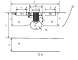
- FIG. 9 is a schematic diagram of device cell structure parameters used in a simulation experiment in Embodiment 1 of the present application.
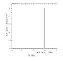
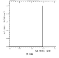
- FIG. 10A and 10B are simulation curves of breakdown voltage of a power semiconductor device provided in Embodiment 1 of the present application, wherein FIG. 10A is a simulation curve of forward breakdown voltage, and FIG. 10B is a simulation curve of reverse breakdown voltage;
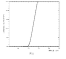
- FIG. 11 is a simulation curve diagram of a threshold voltage of a power semiconductor device provided in Embodiment 1 of the present application.
- FIG. 12 is a simulation result diagram of an on-resistance of a power semiconductor device according to an embodiment of the present application.
- FIG. 13 is a schematic flowchart of a method for manufacturing a power semiconductor device according to the first embodiment of the present application.
- FIGS. 14A to 14I are schematic cross-sectional structure diagrams corresponding to a series of processes in a method for manufacturing a power semiconductor device provided in Embodiment 1 of the present application;
- FIG. 15 is a schematic top view of a power semiconductor device according to a second embodiment of the present application.
- FIG. 16 is a schematic cross-sectional structure view of a power semiconductor device according to the second embodiment of the present application along the I-I direction in FIG. 15; FIG.
- FIG. 17 is a schematic cross-sectional structure view of a power semiconductor device provided in Embodiment 2 of the present application along the II-II direction in FIG. 15; FIG.
- FIG. 18 is a schematic top view of another power semiconductor device provided in Embodiment 2 of the present application.
- FIG. 19 is a schematic cross-sectional structure diagram of another power semiconductor device according to the second embodiment of the present application along the I-I direction in FIG. 18;
- FIG. 20 is a schematic cross-sectional structure view of another power semiconductor device provided in Embodiment 2 of the present application, taken along the II-II direction in FIG. 18; FIG.
- FIG. 21 is a schematic diagram of device cell structure parameters used in a simulation experiment in Embodiment 2 of the present application.
- FIG. 22A and 22B are simulation curves of breakdown voltage of a power semiconductor device provided in Embodiment 2 of the present application, wherein FIG. 22A is a simulation curve of forward breakdown voltage, and FIG. 22B is a simulation curve of reverse breakdown voltage;
- FIG. 23 is a simulation curve diagram of a threshold voltage of a power semiconductor device provided in Embodiment 2 of the present application.
- FIG. 24 is a simulation result diagram of an on-resistance of a power semiconductor device provided in Embodiment 2 of the present application.
- 25 is a schematic flowchart of a method for manufacturing a power semiconductor device according to a second embodiment of the present application.
- 26A to 26I are structural schematic diagrams corresponding to a series of processes in a method for manufacturing a power semiconductor device provided in Embodiment 2 of the present application;
- FIG. 27 is a schematic flowchart of another method for manufacturing a power semiconductor device according to Embodiment 2 of the present application.
- 28A to 28F are schematic cross-sectional structure diagrams corresponding to a series of processes in a method for manufacturing a power semiconductor device provided in Embodiment 2 of the present application.
- FIG. 29A is a schematic diagram of a rectangular-shaped groove provided by the present application.
- FIG. 29B is a schematic diagram of a convex-shaped groove provided by the present application.
- FIG. 30A is a schematic diagram of a gate provided by the present application.
- FIG. 30B is a schematic diagram of another gate provided by the present application.
- FIG. 31A is a schematic diagram of a similar rectangular trench with a gate provided in the present application.
- FIG. 31B is a schematic view of a convex-like groove with a gate provided in the present application.
- FIG. 32A is a schematic diagram of a similar rectangular trench with two gates provided in this application.
- FIG. 32B is a schematic view of a similar convex-shaped trench with two gates provided in the present application.
- FIG. 33 is a schematic front view of a device product provided by the present application.
- FIG. 34 is a schematic diagram of a terminal device provided by the present application.
- Channel refers to a thin semiconductor layer between the source and drain regions in a field effect transistor.
- a power semiconductor device The smallest unit that constitutes a power semiconductor device.
- a power semiconductor device includes multiple cells in parallel.
- N-well region a low-concentration N-type doped region.
- Drift region refers to a high-resistance region with a very small number of carriers in the PN junction under the dual effects of drift motion and diffusion.
- Epitaxial layer refers to a semiconductor layer grown and deposited on a substrate.
- Field plate It is one of the common methods of semiconductor terminal technology. It changes the surface potential distribution to increase the radius of curvature of the surface junction and suppress the surface electric field concentration.
- Depletion layer It is in the vicinity of the PN junction, where the carriers are depleted due to diffusion, leaving only the immovable positive and negative ions, also known as the space charge region.
- RESURF technology Reduced surface electric field (Reduced Surface) technology is the most widely used technology in designing lateral high voltage and low on-resistance devices.
- the power semiconductor devices used by it mainly include two types: discrete solution devices and integrated solution devices.
- the problems with discrete solution devices are low integration, excessive chip height, and high cost.
- the problem with integrated solution devices is that the on-resistance is too large, the losses are serious, or the chip area is too large, and the cost is difficult to accept.
- a common structure of a power semiconductor device in the industry is that two MOS devices with the same structure are connected in series.
- the cross-sectional structure and symbol diagram of the device cell corresponding to this structure are shown in Figure 1 and Figure 2, respectively.
- the source 11 of the two MOS devices is shorted together, and the gates 121 and 122 are shorted together.
- the two drains 131 and 132 are respectively used as the input and output ends of the device.
- the control signals are controlled by the gates 121 and 122.
- the channels of each MOS device are turned on or off at the same time.
- bidirectional blocking withstand voltage refers to the fact that, of the two drains 131 and 132, no matter which one is connected to the positive pole of the power supply and which is connected to the negative pole of the power supply , Can achieve blocking withstand voltage
- the current flows from the drain 131 of one MOS to the drain 132 of the other MOS, the current path is shown by the arrow in FIG. 1.
- the device structure is optimized on the basis of power semiconductor devices commonly used in the industry.
- a schematic diagram of a cell cross section of the optimized device structure is shown in FIG. 3A
- a schematic diagram of a device symbol of the optimized device structure is shown in FIG. 3B.
- this solution addresses the obvious shortcomings of common power semiconductor devices in the industry, combining two gate stages into a single gate stage 31, thereby achieving a single channel, while removing the source region structure and reducing the source region. area. Reduce the on-resistance of the device and reduce the chip area.
- This solution uses a conventional LDMOS structure.
- the disadvantage is that in order to reduce the surface electric field strength and improve the withstand voltage capability of the device, the surface field plate technology must be used.
- the length of the field plate, the length of the drift region 32 and the concentration determine the withstand voltage capability of the device.
- a lower doped and longer drift region must be used. This will increase the cell size of the device and increase the resistance of the drift region. It should be known that higher on-resistance of the device results in lower current density.
- the sum of the length of the bilateral drift region of the withstand voltage device shown in FIG. 3A accounts for 80% of the cell size, and the resistance of the drift region accounts for about 60% of the on-resistance.
- the chip area is reduced.
- a trench gate structure is used to set a channel at the bottom of the trench, and the vertical field plate and the double vertical RESURF technology of the vertical PN structure are used to achieve the purpose of reducing the size of the cell drift region and increasing the concentration of the drift region, thereby achieving reduction.
- Cell size and the effect of reducing the resistance of the drift region utilizes a traditional low-cost manufacturing technology to realize a MOS-type switching device having a low on-resistance and a high bidirectional withstand voltage.
- FIG. 4 is a top view of a power semiconductor device provided in Embodiment 1 of the present application
- FIG. 5 is a schematic cross-sectional structure diagram of a power semiconductor device provided in Embodiment 1 of the present application
- the power semiconductor device includes:
- a P-type channel 59 which is located between the bottom wall of the trench 53 and the substrate 51 and adjacent to the bottom wall of the trench 53.
- the trench 53 is located in the epitaxial layer 52 and is close to the outer surface region of the epitaxial layer 52, and the opening of the trench 53 faces the outer surface of the epitaxial layer 52.
- the specific structure of the trench 53 may be as follows: along the thickness direction of the epitaxial layer 52, the trench 53 may include a main body portion 531 and a protruding portion 532 extending from the main body portion 531 and protruding toward the substrate 51. It should be understood that the width of the main body portion 531 is larger than the width of the protruding portion 532.
- the structure of the trench 53 can also be understood in the following manner: the trench is a convex groove, the convex portion of the convex groove projects toward the substrate, and the opening of the convex groove faces the upper surface of the epitaxial layer.
- the field oxide layer 55 may include a first field oxide layer 551 along a sidewall of the main body portion 531 and a second field oxide layer 552 along a sidewall of the convex portion 532; and, In order to reduce the on-resistance of the semiconductor device while ensuring the withstand voltage, the thickness of the first field oxide layer 551 is greater than the thickness of the second field oxide layer 552.
- the N-type drift region 57 is located at the periphery of the groove body portion 531 and the convex portion 532 accordingly.
- the first field oxide layer 551 may be formed by depositing silicon dioxide using an oxide deposition process.
- the second field oxide layer 552 can be formed by a thermal oxidation method.
- the second field oxide layer 552 may be formed simultaneously with the gate oxide layer 56.
- the thickness of the first field oxide layer 551 may be to between.
- the P-type channel 59 may be formed by implanting P-type doped ions into the bottom of the protruding portion 532 of the trench 53 by ion implantation.
- the width of the gate electrode 54 in the thickness direction of the epitaxial layer may be uniform.
- the width of the gate electrode in the thickness direction of the epitaxial layer may also be inconsistent.
- the gate electrode 54 may include a first portion and a second portion extending from the first portion to the bottom wall of the trench 53 in the thickness direction of the epitaxial layer.
- the width of the first portion is greater than the width of the second portion.
- the first portion of the gate is located in the main body portion 531 of the trench, and the second portion of the gate is located in the protruding portion 532 of the trench.
- the gate 54 may be a polysilicon gate.
- the first drain electrode 581 and the second drain electrode 582 are symmetrically distributed on both sides of the trench 53.
- the body electrode 510 is located in the epitaxial layer 52 and is close to the outer surface of the epitaxial layer 52.
- the body electrode 510 can be formed by ion implantation of P-type doped impurities in the epitaxial layer 52.
- the body electrode 510 can also be understood as a P-type shallow well formed in the epitaxial layer 52 by ion implantation.
- a power semiconductor device provided in Embodiment 1 of the present application includes a plurality of cells 50 and a body electrode 510 connected in parallel.
- the body electrode 510 is located in a peripheral region of the cell 50.
- the cells 50 are located in the enclosed area of the body electrode 510.
- one cell 50 may be located in the enclosed area of the body electrode 510, or a plurality of cells 50 may be located in the enclosed area of the body electrode 510.
- the cells 50 surrounded by the body electrode 510 share one body electrode.
- the body electrode 510 is located in a peripheral region of all the cells 50, that is, all the cells 50 are replaced by a body electrode 510. Surrounding, all the cells 50 share one body electrode 510.
- the power semiconductor device includes N cells 50 connected in parallel, and N is an integer greater than or equal to 2.
- the power semiconductor includes a substrate and an epitaxial layer.
- the epitaxial layer has a trench, a channel, and a drift region.
- the drift region has a first drain and a second region.
- the drain and a gate in the trench, and an oxide layer between the inner wall of the trench and the outer wall of the gate can be understood as a limitation on the structure of the cells located in the power semiconductor device.
- the doping types of the substrate, the epitaxial layer, and the channel are all P-type, and the drift region, the first drain, and the first The doping types of the two drains are all N-type.
- the doping types of the substrate, the epitaxial layer, and the channel are all N-type, and the doping types of the drift region, the first drain electrode, and the second drain electrode are all N-type. All are P-type.
- the electrodes are led out to the upper surface of the device, and the signal transmission is realized by a method of planting a ball on the surface. Then, a wafer-level chip package (WLCSP) is used to implement the final device product.
- WLCSP wafer-level chip package
- reference numeral in FIG. 7 or FIG. 33 is used to indicate the external pin of the corresponding electrode
- the reference numeral 510 is used to indicate the external pin of the body electrode 510
- the reference numeral 54 is used to indicate the gate electrode.
- Reference numeral 581 is used for the external pin of the first drain electrode 581
- reference numeral 582 is used for the external pin of the second drain electrode 582.
- one column of first drain electrodes 581 is followed by one column of second drain electrodes 582, that is, a column formed by a plurality of first drain electrodes 581 and a plurality of second drain electrodes 582.
- the formed columns are arranged alternately.
- one or more columns of first drain electrodes 581 are located on one side of the gate 54
- one or more columns of second drain electrodes 582 are located on the other side of the gate 54.
- the parasitic resistance of the metal trace can be reduced.
- FIG. 8 a three-dimensional schematic diagram of a final device product formed by a wafer-level chip packaging method in this application is shown in FIG. 8.
- the package structure includes a chip 81 and a back coating layer 82 on a back surface of the chip 81.
- a plurality of solder balls 811 are provided on the front surface of the chip 81 for signal transmission with the outside.
- the height of the WLCSP device is about 0.5mm (the back layer is about 0.04mm, the thickness of the silicon wafer is about 0.25mm, and the height of the solder ball is 0.2mm), which is only half of the height of the plastic packaged device.
- the heat dissipation effect of WLCSP devices is also better than that of plastic-packaged devices of the same size.
- the thermal resistance Rja of a WLCSP device of 2mm x 2mm 25 balls is about 30 ° C / W, which is only half that of a plastic-packaged package of the same size.
- the power semiconductor device is a passive MOS structure, and the removal of the source region is conducive to reducing the cell size, and the reduction in cell size is beneficial to reducing the unit area of the power semiconductor device. On-resistance.
- the power semiconductor device has a single-channel structure (such as channel 59 shown in FIG. 5).
- the single-channel configuration is beneficial to reduce the channel resistance and the cell on-resistance.
- the field oxide layer is provided inside the epitaxial layer (device body) to form a vertical field plate (vertical field oxide layer) in the body, and the drift region 57 and the epitaxial layer 52 in the power semiconductor device form the body.
- Longitudinal PN junction in-body longitudinal diode. Therefore, the present application uses the dual RESURF technology of the vertical field plate in the body and the vertical P / N junction in the body, which greatly reduces the chip area.
- the so-called longitudinal direction in the previous paragraph refers to the thickness direction of the substrate, the thickness direction of the epitaxial layer, or the depth direction of the trench.
- the formation of vertical diodes in the device makes the device free of surface strong electric field problems and does not require surface field plate technology, which is conducive to reducing the lateral size of the drift region and thus the cell size.
- the device uses a vertical gate field oxide layer and uses a charge balance mechanism to help increase the concentration of the drift region, thereby reducing the resistance of the drift region, thereby reducing the cell on-resistance.
- the power semiconductor device provided in this application can reduce the on-resistance per unit area of the power semiconductor device, reduce the chip area, and reduce the power loss of the device.
- the cross-sectional shape of the groove may be rectangular or convex, and naturally may be other shapes. It should be noted that the plane where the cross section of the trench is located is perpendicular to the length direction of the trench. In order to facilitate the understanding of what is described below, the terms that will appear below are explained first.
- the length direction of the groove refers to an extending direction of the groove.
- a depth direction of the trench is perpendicular to a width direction of the trench.
- the depth of the trench and the width of the trench are both based on the concept of the cross-section of the trench. It should be noted that both the depth direction of the trench and the width direction of the trench are located in the plane where the cross section of the trench is located. Naturally, the depth direction of the groove and the width direction of the groove are both perpendicular to the length direction of the groove.
- the cross-sectional shape of the groove may be rectangular, or other shapes close to a rectangle (or a similar rectangle).
- the cross-sectional shape of the groove is similar to a rectangle.
- the width of the groove bottom of the groove is contracted (or gradually becomes smaller) along the depth direction of the groove. ).
- the width of other parts in the groove except the groove bottom is equal or approximately equal.
- the bottom of the trench is a curve close to an arc. It is worth noting that when the cross-sectional shape of the groove is referred to as rectangular or nearly rectangular, the restrictions in this paragraph can be referred to. No more explanation.
- the shape of the cross section of the groove is close to a convex shape, which is referred to as a convex shape for short.
- the convex shape includes a main body portion and a protruding portion. It should be explained that the width of the main body portion is larger than the width of the protruding portion.
- the width of the main body portion is equal (or approximately equal), and the width of the bottom of the protruding portion (or the bottom of the groove called the groove) is contracted in the depth direction of the groove . Referring to FIG. 29B, it can be easily seen that the width of the other portions of the protrusion except the bottom is equal or substantially equal.
- the cross-sectional shape of the trench there may be only one gate in the trench.
- An oxide layer is provided between the outer side wall of the gate and the inner side wall of the trench, and between the bottom surface of the gate and the bottom of the trench.
- the material of the oxide layer is silicon dioxide. It is worth noting that the bottom surface of the gate is toward the bottom of the trench.
- the oxide layer between the outer wall of the gate and the inner wall of the trench is a first oxide layer (or, there is a first oxide layer between the outer wall of the gate and the inner wall of the trench. ), And the oxide layer between the bottom surface of the gate and the groove bottom of the trench is a second oxide layer (or, there is a second oxide layer between the bottom surface of the gate and the groove bottom of the trench). It should be noted that the second oxide layer is a gate oxide layer.
- the first oxide layer is a gate oxide layer or a field oxide layer.
- the first oxide layer may include both a gate oxide layer and a field oxide layer.
- the first oxide layer is a gate oxide layer.
- the so-called roughly equal should follow the conventional understanding of those skilled in the art. If the thickness of the first oxide layer is significantly larger than the thickness of the second oxide layer, for example, the difference between them can be judged by the naked eye, the first oxide layer is a field oxide layer.
- Shape of the gate groove bottom shape of the groove bottom surface are the same or substantially the same.
- the width of the bottom surface of the gate is gradually reduced (or gradually reduced). It should be known that when the gate is located in the trench, the width of the bottom surface of the gate gradually shrinks (or gradually becomes smaller) along the depth direction of the trench.
- the gate may be entirely located within the trench, or may be partially located within the trench (or a portion of the gate protruding outside the trench).
- the so-called “there is a first oxide layer between the outer sidewall of the gate and the inner sidewall of the trench” means that along the width direction of the trench, A first oxide layer is provided between the region of the inner sidewall of the trench that is directly opposite the outer sidewall of the gate and the outer sidewall of the gate.
- the gate portion is located in the trench and the other portion is located outside the trench (it can be understood that the gate portion is protruding outside the trench), then the so-called “outside of the gate
- a first oxide layer is provided between the paired region and an outer sidewall of a portion of the gate electrode located in the trench.
- the top surface of the gate may be flush with the slot of the trench or protrude from the slot of the trench, or may be located in the trench Inside the slot.
- the top surface of the gate is flush with or protrudes from the slot of the trench.
- a first oxide layer is provided between an inner sidewall of the trench and an outer sidewall of the gate. It should be explained that the upper edge of the inner wall of the trench is the plane on which the outer surface of the epitaxial layer is located, and the lower edge of the inner wall of the trench is the edge of the bottom surface of the gate.
- the cross-sectional shape of the trench is close to a rectangular shape
- the first oxide layer is a gate oxide layer or a field oxide layer.
- the first oxide layer may include both a gate oxide field and a field oxide. Floor.
- the first oxide layer includes both a gate oxide layer and a field oxide layer
- the trench is along a direction from a slot opening of the trench to a bottom of the trench.
- the slot notch is located above the slot bottom of the trench (or, assuming that the slot bottom of the trench is located below the slot notch of the trench)
- the field oxide layer is located at the gate oxide layer
- the field oxide layer is located at an upper portion of the inner sidewall of the trench
- the gate oxide layer is located at a lower portion of the inner sidewall of the trench.
- a cross-sectional shape of the trench is close to a convex shape, a portion of the first oxide layer located on the main body portion is a field oxide layer, and a portion of the first oxide layer located on the protruding portion is a gate oxide layer.
- a top surface of the gate is located in the trench.
- a first oxide layer is provided between at least a portion of an inner sidewall of the trench and an outer sidewall of the gate.
- An upper edge of the at least part of the inner sidewall is aligned with an edge of a top surface of the gate, and a lower edge of the at least part of the inner wall side is aligned with an edge of a bottom surface of the gate. It should be known that the upper edge of the at least part of the inner side wall is opposite to the lower edge of the at least part of the inner side wall.
- the cross-sectional shape of the trench is close to a rectangle
- the first oxide layer is a gate oxide layer or a field oxide layer.
- the first oxide layer may further include both a gate oxide layer and a field oxide layer.
- the field oxide layer is located on an upper portion of an inner sidewall of the trench, and the gate oxide layer is located on The lower portion of the inner side wall of the groove.
- a cross-sectional shape of the trench is close to a convex shape, a portion of the first oxide layer located on the main body portion is a field oxide layer, and a portion of the first oxide layer located on the protruding portion is a gate oxide layer.
- an insulating layer is provided in a region between an extension surface of a top surface of the gate and a plane on which an outer surface of the epitaxial layer is located. It is worth explaining that the extending surface of the top surface of the gate includes a surface obtained after the edge of the gate extends in the width direction of the trench and the top surface of the gate.
- the insulating layer may be an oxide layer.
- the insulating layer is silicon dioxide. You can refer to the explanation here when the insulation layer appears again later.
- the plurality of gates are electrically connected, and the plurality of gates are arranged in a depth direction of the trench.
- the plurality of gates are discontinuous.
- the gate farthest from the bottom of the trench of the plurality of gates may be referred to as a top gate, and a top surface of the top gate may be aligned with a slot of the trench. Flat or protruding beyond the notch of the groove, it may also be located inside the groove.
- the gate closest to the bottom of the trench of the plurality of gates may also be referred to as a bottom gate, and a bottom surface between the bottom surface of the bottom gate and the bottom of the trench has a first gate. Dioxide layer. It can be known from the foregoing that the second oxide layer is a gate oxide layer.
- the top surface of the top gate is flush with the notch of the trench or protrudes beyond the notch of the trench.
- the first oxide layer between the outer sidewall of the bottom gate and the inner sidewall of the trench is a gate oxide layer. It should be known that, assuming that a region of the inner sidewall of the trench that is directly opposite the outer sidewall of the bottom gate is the bottom region, the first region between the outer sidewall of the bottom gate and the inner sidewall of the trench is The oxide layer is a gate oxide layer. Specifically, the first oxide layer between the outer sidewall of the bottom gate and the bottom region is a gate oxide layer. Similar descriptions mentioned elsewhere in this application should also be understood as explained here.
- a first oxide layer between an outer sidewall of each of the gates except the bottom gate and an inner sidewall of the trench is a field oxide layer.
- the width of the plurality of gates gradually decreases in a direction from a bottom of the trench to a slot of the trench.
- the direction in which the width of the gate is located is perpendicular to the depth direction of the trench.
- a region between two adjacent gates is extended after the width of the trench is obtained.
- a top surface of the top gate is located in the trench.
- an insulating layer is provided in a region between an extension surface of a top surface of the top gate and a plane on which an outer surface of the epitaxial layer is located. It is worth explaining that the extending surface of the top surface of the top gate includes a surface obtained after the edge of the top gate extends in the width direction of the trench and the top surface of the top gate.
- the cross-sectional shape of the trench is close to a rectangle (or a similar rectangle), and there are two gates in the trench, and the two gates are electrically connected, and The gates are arranged along the depth of the trench.
- the two gates are discontinuous.
- the two gates can be an upper gate and a lower gate, respectively.
- a region in the inner sidewall of the trench that is directly opposite the outer sidewall of the upper gate may also be referred to as an upper region, and the inner sidewall of the trench and the lower gate may be referred to as an upper region.
- the area directly opposite the outer wall is called the lower area.
- the “bottom surface of the gate” in “Between the bottom of the trench and the bottom surface of the gate” described earlier "Means the bottom surface of the lower gate. Accordingly, the “bottom surface of the gate” in “the bottom surface of the gate faces the bottom of the trench” also refers to the bottom surface of the lower gate.
- the first oxide layer between the lower region and an outer sidewall of the lower gate is a gate oxide layer
- the first oxide layer between the upper region and an outer sidewall of the upper gate is a gate oxide layer
- An oxide layer is a field oxide layer.
- the first oxide layer between the lower region and the outer sidewall of the lower gate is a field oxide layer
- the first oxide layer between the upper region and the outer sidewall of the upper gate is a field oxide layer.
- An oxide layer is a field oxide layer.
- an area between the two gates extending in a width direction of the trench and obtained in the trench and having an insulating layer in the trench.
- the cross-sectional shape of the trench is close to a convex shape (or similar to the convex shape), and the trench has two gates, an upper gate and a lower gate.
- the upper gate is located at a main portion of the trench, and the lower gate is located at a protruding portion of the trench.
- the first oxide layer between the outer sidewall of the lower gate and the inner sidewall of the protruding portion is a gate oxide layer, and the distance between the outer sidewall of the upper gate and the inner sidewall of the main portion is The first oxide layer is a field oxide layer.
- the region between the two gates extends in the width direction of the trench, and the region located in the trench has Insulation.
- the top surface of the upper gate is located in the trench.
- the trench further includes an insulating layer.
- the insulating layer is located in a top region, where the top region refers to a region between an extension surface of a top surface of the upper gate and a plane on which an outer surface of the epitaxial layer is located.
- the extended surface of the top surface of the upper gate includes a surface obtained by extending an edge of the upper gate in a width direction of the trench and a top surface of the upper gate.
- the power semiconductor device provided in this application is based on the dual RESURF technology of the vertical field plate and the vertical diode structure in the body, which greatly reduces the chip area.
- the switching speed is fast, and as an overvoltage protection device, the safety is high; in terms of reliability, the withstand voltage of the power stage and the gate of the present invention is the same as the forward and reverse withstand voltage of the device, and no gate oxide layer is degraded or damaged. Wear reliability risk.
- the device structure and performance parameters of the embodiment of the present application were simulated by semiconductor TCAD (technology computer design, semiconductor device and process simulation tool) simulation.
- This simulation experiment uses a lateral MOS semiconductor device with a bidirectional blocking voltage of 28V trench gate.
- the cell structure parameters of the device are shown in Figure 9 and Table 2: On a P-type substrate with a concentration of 7 * 10 19 , the doping concentration is set to 8 * 10 15 and the thickness is "3" (where 3 refers to the table Reference numeral 3 in 2) is a 2um P-type epitaxial layer to form a device body. An N-type drift region having a concentration of 1.1 * 10 17 is formed on the surface of the device body.
- the depth “4” (here, 4 refers to the number 4 in Table 2) is 0.5um
- the lateral width is “1” (here 1 is Refers to the reference number 1 in Table 2) is 1.3um
- the width of the first part of the trench "6" (here 6 refers to the reference number 6 in Table 2) is 0.3um
- the depth "9” (here 9 refers to the table
- the reference number 9 in 2) is 0.25um
- the width "7" of the second part (7 here refers to the reference number 7 in Table 2) is 0.2um
- the depth "8" (here 8 refers to the value in Table 2).
- the reference number 8) is 0.3 um
- the concentration of the first doped type P-type well region is 1.6 * 10 17
- the depth “10” (here 10 refers to the reference number 10 in Table 2) is 0.4 um
- the field oxide layer The thickness "11” (here 11 refers to the number 11 in Table 2) is set to
- the gate oxide is set to
- the channel length of the device is substantially equal to the width of the second part of the trench, which is 0.2um.
- the threshold voltage of the device depends on the thickness of the gate oxide layer and the concentration of the first doped type P-type well region.
- the breakdown voltage and on-resistance of the device are determined by factors such as the concentration, depth, and length of the N-type drift region, the thickness of the field oxide layer, and the depth of the trench.
- FIG. 10A and FIG. 10B are simulation curve diagrams of breakdown voltage of a power semiconductor device according to the first embodiment of the present application.
- 10A is a simulation curve of the breakdown voltage of the device from the first drain 581 to the second drain 582
- FIG. 10B is a simulation curve of the breakdown voltage of the device from the second drain 582 to the first drain 581.
- the voltage of the first drain 581 gradually increases from 0V, and the current of the first drain 581 is gradually read.
- the sudden increase in the current of a drain 581 increases the voltage of the first drain 581 corresponding to the breakdown voltage of the first drain 581 to the second drain 582 of the device.
- the forward voltage of the device is the first drain 581.
- the breakdown voltage to the second drain 582 is 30V.
- the reverse breakdown voltage of the device that is, the breakdown voltage of the second drain 582 to the first drain 581 is 30V, as shown in FIG. 10B.
- the first embodiment of the present application also provides a threshold voltage simulation experiment of a 28V bidirectional blocking trench lateral MOS semiconductor device.
- the simulation curve is shown in FIG. 11.
- the simulation experiment conditions are: the channel region 59 and the second drain 582 are connected to the bottom at the same time, the first drain 581 is connected to a fixed voltage of 1V, the gate voltage is gradually increased from 0V, and the current of the first drain 581 is gradually read.
- a sudden increase in the drain 581 current corresponding to the gate voltage is the turn-on threshold voltage of the device.
- the simulation result of the threshold voltage is 1.5V.
- the first embodiment of the present invention also provides a measurement (calculation) experiment of a 28V bidirectional blocking trench lateral MOS semiconductor device.
- the simulation conditions of the measurement (calculation) experiment are: the channel and the second drain 582 are connected to the bottom at the same time, the gate voltage is a fixed value of 3.6V or 5V, and the IV characteristics of the voltage and current of the first drain 581 are simulated.
- R V / I calculates the on-resistance of the device from the first drain 581 to the second drain 582.
- the simulation calculation results are shown in Fig. 12.
- the on-resistance per unit area of the device is 8.5m ⁇ .mm2 at a gate voltage of 5V, and 10m ⁇ .mm2 at a gate voltage of 3.6V.
- the on-resistance per unit area of the power semiconductor device provided in Embodiment 1 of the present application is greatly reduced.
- the power semiconductor in the embodiment of this application The on-resistance per unit area of the device is 10m ⁇ .mm2, which is 50% lower than the best commercial devices in the industry.
- Embodiment 1 of the present application further provides a specific implementation manner of the method for manufacturing a power semiconductor device.
- the power semiconductor device provided in the first embodiment of the present application can be implemented based on a traditional discrete trench MOS process or a monolithic integrated BCD process technology, and the manufacturing process is simple and the manufacturing cost is low.
- FIG. 13 is a schematic flowchart of a method for manufacturing a power semiconductor device according to the first embodiment of the present application.
- 14A to 14I are schematic cross-sectional structure diagrams corresponding to a series of processes in a method for manufacturing a power semiconductor device provided in Embodiment 1 of the present application.
- the manufacturing method of the power semiconductor device includes:
- S131 Provide a P-type substrate.
- the P-type substrate 51 may be a silicon substrate.
- FIG. 14A A schematic cross-sectional structure of a P-type substrate is shown in FIG. 14A.
- a P-type epitaxial layer is formed over the P-type substrate; the epitaxial layer includes a first region and a second region located outside the first region.
- This step may be specifically: growing a P-type epitaxial layer 52 with a certain doping concentration on the P-type substrate 51.
- the first region refers to a region in which cells are located
- the second region refers to a contact region of a body electrode. As shown in FIG. 4, a region where the cell 50 is located is the first region, and a contact region of the body electrode 510 is the second region.
- the P-type epitaxial layer 52 can be used as a device body.
- the P-type epitaxial layer 52 includes a first region I and a second region II.
- a schematic cross-sectional structure diagram after the execution of this step is shown in FIG. 14B.
- S133 An N-well is formed in the first region of the epitaxial layer and near the upper surface of the epitaxial layer.
- This step may be specifically: implanting N-type doped impurity ions inside the first region I on the epitaxial layer 52 and close to the upper surface of the epitaxial layer by ion implantation to form an N well 57 ′ in the first region of the epitaxial layer 52 An N-type drift region is formed on I and near the upper surface of the epitaxial layer.
- FIG. 14C A schematic cross-sectional structure diagram after the execution of this step is shown in FIG. 14C.
- the N-well 57 ' is etched by a silicon etching process to form a main body portion 531 of the trench in the N-well 57'.
- the corresponding cross-sectional structure diagram after performing this step is shown in FIG. 14D.
- S135 can be implemented through the following implementations, which includes the following steps:
- the main body 531 is filled with silicon dioxide 150 by using a thermal growth or silicon dioxide deposition process.
- a schematic cross-sectional structure diagram after performing this step is shown in FIG. 14E.
- S1352 Etching silicon dioxide located in a middle region of the main body portion to form a first field oxide layer on a sidewall of the trench main body portion.
- This step may be specifically: etching the silicon dioxide 150 located in the middle region of the main body portion 531 according to the thickness of the first field oxide layer to form a first field oxide layer 551 on the sidewall of the main body portion 531.
- the thickness of the first field oxide layer determines the withstand voltage performance of the power semiconductor device. Therefore, the thickness of the first field oxide layer can be determined according to the withstand voltage performance of the power semiconductor device. As an example, the thickness of the first field oxide layer may be 0.1 ⁇ m.
- This step may be specifically: etched from the bottom of the main body portion having the first field oxide layer formed on the sidewall toward the substrate by using a silicon etching process, thereby forming a protruding portion 532 of the trench. It should be noted that the protruding portion 532 of the trench may extend into the epitaxial layer 52.
- the main body portion 531 and the protruding portion 532 constitute a groove 53.
- an N-well 57 'located at the periphery of the trench body portion 531 and the protruding portion 532 is formed as the drift region 57.
- FIG. 14F A schematic cross-sectional structure diagram after the execution of step S136 is shown in FIG. 14F.
- a trench is formed in a region between the bottom wall of the trench and the substrate and adjacent to the bottom wall of the trench.
- This step may be specifically: implanting P-type doping ions into the bottom wall of the protruding portion 532 to form P in a region between the bottom wall of the protruding portion 532 and the substrate 51 and adjacent to the bottom wall of the trench protruding portion 532.
- a type well region 59 is used as a channel 59 of the power semiconductor device.
- FIG. 14G The schematic diagram of the cross-sectional structure after the execution of this step is shown in FIG. 14G.
- S138 forming an oxide layer on the inner surface of the convex portion of the trench to form a second field oxide layer on the sidewall of the convex portion, and forming a gate oxide layer on the bottom wall of the convex portion.
- the function of the oxide layer formed on the bottom surface of the protruding portion 532 is a gate oxide layer.
- the quality and thickness of the gate oxide layer play a key role in the threshold voltage of the gate. Therefore, in order to improve the film quality of the generated oxide layer, this step may be specifically: forming an oxide layer on the inner surface of the protruding portion 532 by a thermal growth process.
- An oxide layer can be formed on the bottom and sidewalls of the protruding portion 532 through a thermal growth process.
- the oxide layer formed on the bottom surface of the protruding portion 532 is the gate oxide layer 56, and the oxide layer formed on the sidewall of the protruding portion 532 is the second field oxide layer 552.
- the oxide layer formed on the inner surface of the protruding portion 532 is a thin layer oxide layer.
- the thickness of the oxide layer is smaller than the thickness of the first field oxide layer formed on the sidewall of the main body portion 531.
- the thickness of the second field oxide layer is smaller than the thickness of the first field oxide layer. In this way, it is possible to have a small on-resistance while ensuring the threshold voltage and withstand voltage of the power semiconductor device.
- FIG. 14H A schematic cross-sectional structure diagram corresponding to the execution of this step is shown in FIG. 14H.
- S139 Fill the trench with a gate electrode material to form a gate electrode.
- This step may be specifically: depositing and filling polysilicon into the trench 53 to form a polysilicon gate electrode 54 in the trench 53. It should be noted that after filling the polysilicon, in order to reduce the mask plate, the polysilicon can also be polished by a chemical mechanical polishing process after the polysilicon is filled.
- the width of the formed gate electrode 54 in the thickness direction of the epitaxial layer may be uniform.
- the width of the gate electrode in the thickness direction of the epitaxial layer may also be inconsistent.
- the gate electrode 54 may include a first portion and a second portion extending from the first portion to the bottom wall of the trench 53 in the thickness direction of the epitaxial layer.
- the width of the first portion is greater than the width of the second portion.
- the first portion of the gate is located in the main body portion 531 of the trench, and the second portion of the gate is located in the protruding portion 532 of the trench.
- FIG. 14I The corresponding cross-sectional structure diagram after this step is performed is shown in FIG. 14I.
- S1310 Form a first N-type drain and a second N-type drain in the drift regions on both sides of the trench, respectively.
- This step may be specifically: implanting heavily doped N-type doped ions into the surfaces of the drift regions on both sides of the trench, thereby forming a first N-type drain 581 and a second N-type in the drift regions on both sides of the trench. Drain 582. It should be noted that, as a specific example, the first N-type drain 581 and the second N-type drain 582 may be symmetrically distributed on both sides of the trench to form a bidirectional withstand voltage MOS switching device.
- a P-type doped ion may be implanted into the surface in the second region of the epitaxial layer 52 to form a P-type heavily doped well.
- the hybrid well serves as a P-type body electrode 510. It should be noted that, in the embodiment of the present application, all cells are located in a surrounding area of the body electrode 510.
- FIG. 5 A schematic cross-sectional structure diagram after the execution of this step is shown in FIG. 5.
- Embodiment 1 of the present application is a specific implementation manner of a method for manufacturing a power semiconductor device provided in Embodiment 1 of the present application.
- this specific implementation manner it can be implemented based on the traditional separated trench gate MOS process or the monolithic integrated BCD process technology, the manufacturing process is simple, and the manufacturing cost is low.
- the present application also provides another specific implementation manner of a power semiconductor device and a manufacturing method thereof. For details, see Embodiment 2.
- FIG. 15 is a schematic top view of a power semiconductor device provided in Embodiment 2 of the present application
- FIG. 16 is a schematic cross-sectional structure view of a power semiconductor device provided in Embodiment 2 of the present application along the II direction in FIG.
- FIG. 17 is A schematic cross-sectional structure of a power semiconductor device provided in the second embodiment of the application along the II-II direction in FIG. 15.
- a power semiconductor device provided in Embodiment 2 of the present application includes:
- a P-type epitaxial layer 172 disposed on one side of the substrate 171;
- a trench 173 is provided in the epitaxial layer 172.
- the trench 173 includes an island-shaped P-type well region 174 and a gate electrode 175 inside.
- a specific area of the bottom wall is covered with a gate oxide layer 177, and the specific area is an area covered by the orthographic projection of the bottom surface of the gate 174 on the bottom wall of the trench 173;
- N-type drift regions 178 disposed on both sides of the trench 173, wherein the field oxide layer 176 and the drift region 178 overlap in the lateral direction of the cell;
- the device may further include a body electrode 1711 formed in the P-type well region 174.
- the body electrode 1711 is formed in the P-type well region 174 and is close to the outer surface of the P-type well region 174.
- the doping type of the body electrode 1711 is P-type. In this way, a body electrode is formed on each cell, and a cell having a body electrode is formed. In this way, the current sharing between cells is improved.
- a field oxide layer 176 may be provided around the P-type well region 174.
- the P-type channel 1710 and the P-type well region 174 may be formed at the same time, and the two may be an integrated molding structure, which may be formed by implanting doped ions from a part of the surface of the epitaxial layer. It can be considered that the P-type channel 1710 and the P-type well region 174 are different portions of the P-type well region formed by implanting P-type doped ions from a partial region on the surface of the epitaxial layer, respectively. The specific implementation manner will be described in detail in the manufacturing method of the power semiconductor device.
- the width of the gate electrode 175 in the thickness direction of the epitaxial layer may be uniform.
- the width of the gate electrode 175 in the thickness direction of the epitaxial layer may be inconsistent.
- the gate electrode 175 may include a first portion and a second portion extending from the first portion to the bottom wall of the trench 173 in the thickness direction of the epitaxial layer.
- the width of the first portion is greater than the width of the second portion.
- the first portion of the gate is located in the main body portion 1731 of the trench, and the second portion of the gate is located in the protruding portion 1732 of the trench.
- the gate 175 may be a polysilicon gate.
- the first drain electrode 1791 and the second drain electrode 1792 are symmetrically distributed on both sides of the trench 173.
- the widths of the trenches 173 in the thickness direction of the epitaxial layer may be uniform.
- the longitudinal cross-sectional shape of the trench 173 is rectangular. In this way, the formation of the trench can be formed by sequential etching processes, the manufacturing process is relatively simple, and the manufacturing cost is relatively low.
- the widths of the trenches 173 along the thickness direction of the epitaxial layer may also be inconsistent.
- the groove 173 is a convex groove.
- the structure of the semiconductor device of this alternative embodiment is shown in FIGS. 18 to 20.
- FIG. 18 is a schematic top view of another power semiconductor device provided in Embodiment 2 of the present application
- FIG. 19 is another power semiconductor device provided in Embodiment 2 of the present application along FIG. 18.
- FIG. 20 is a schematic cross-sectional structure diagram along the II-direction in FIG. 20, which is another power semiconductor device provided in Embodiment 2 of the present application.
- FIGS. 18 to 20 has many similarities to the structure of the power semiconductor device described in FIGS. 15 to 17, and the difference is only in the shape of the trench. For brevity, only the differences are described here.
- the trench 173 may include a main body portion 1731 and a protruding portion 1732 extending from the main body portion 1731 and protruding toward the substrate 171. It should be understood that the width of the main body portion 1731 is larger than the width of the protruding portion 1732.
- the structure of the trench 173 can also be understood in the following manner: the trench is a convex groove, the convex portion of the convex groove projects toward the substrate, and the opening of the convex groove faces the upper surface of the epitaxial layer.
- the field oxide 176 may include a first field oxide layer 1761 along a sidewall of the main body portion 1731 and a second field oxide layer 1762 along a sidewall of the convex portion 1732; To reduce the on-resistance of the semiconductor device, the thickness of the first field oxide layer 1761 is greater than the thickness of the second field oxide layer 1762.
- the N-type drift region 178 is located at the periphery of the groove body portion 1731 and the convex portion 1732.
- the first field oxide layer 1761 may be formed by depositing silicon dioxide using an oxide deposition process.
- the second field oxide layer 1762 may be formed by thermal oxidation.
- the second field oxide layer 1762 may be formed simultaneously with the gate oxide layer 177.
- the power semiconductor device provided in the second embodiment of the present application.
- the power semiconductor device in addition to the beneficial effects of the power semiconductor device provided in the first embodiment, the power semiconductor device also has better current sharing between cells.
- the semiconductor device TCAD simulation is used to simulate the device structure and performance parameters of the present embodiment.
- This simulation experiment uses a lateral MOS semiconductor device with a bidirectional blocking voltage of 28V trench gate.
- the device cell structure parameters are shown in Figure 21 and Table 3:
- a P-type epitaxial layer forming device having a doping concentration of 8 * 10 15 and a thickness of "3" (where 3 refers to the number 3 in Table 3) is 2um is set. Ontology.
- the width of the first part of the trench "7" (here 7 refers to the number 7 in Table 3) is 0.4um, and the depth “9” (here 9 refers to the number 9 in Table 3) is 0.2um
- the second The width of the part “6” (6 here refers to the number 6 in Table 3) is 0.3um, and the depth “8" (here 8 refers to the number 8 in Table 3) is 0.2um
- N-type drift regions with a concentration of 8 * 10 16 are set on both sides of the trench
- the depth "4" (5 here refers to the number 5 in Table 3) is 0.5um
- the lateral width "5" (here 5 refers to the reference numeral 7) in Table 5 is 0.5um.
- the concentration of the first doped type P-type well region is 1.7 * 10 17
- the depth “10” (10 here refers to the number 10 in Table 3) is 0.9um
- the field oxide layer thickness “11” (here 11 refers to the reference number 11 in Table 3)
- Gate oxide thickness is The channel length of the device is substantially equal to the width of the second part of the trench, which is 0.3um.
- the threshold voltage of the device depends on the thickness of the gate oxide layer and the concentration of the first doped type P-type well region.
- the breakdown voltage and on-resistance of a device are determined by factors such as the concentration, depth, and length of the N-type drift region, the thickness of the field oxide layer, and the depth of the trench.
- 22A and 22B are simulation curve diagrams of device breakdown voltage in the second embodiment.
- the voltage of the first drain gradually rises from 0V, and the current of the first drain 1791 is gradually read, and the first drain 1791
- the sudden increase of the current corresponds to the breakdown voltage of the first drain 1791 to the breakdown voltage of the first drain 1791 to the second drain 1792.
- the forward voltage of the device is the first drain 1791 to the second.
- the breakdown voltage of the drain 1792 is 29V.
- the reverse breakdown voltage of the device that is, the breakdown voltage of the second drain 1792 to the first drain 1791 is 29V, as shown in FIG. 22B.
- the threshold voltage simulation curve of the device according to the second embodiment of the present invention is shown in FIG. 23.
- the channel 1710 and the second drain 1792 are connected to the bottom at the same time.
- the first drain 1791 is connected to a fixed voltage 1V, and the gate voltage is gradually increased from 0V.
- the current of the first drain 1791 is read.
- the sudden increase in the current of the first drain 1791 increases the corresponding gate voltage to be the turn-on threshold voltage of the device.
- the simulation result of the threshold voltage is 1.5V.
- Embodiment 2 of the present invention also provides a measurement (simulation calculation) experiment of a 28V bidirectional blocking trench lateral MOS type semiconductor device.
- the simulation conditions of this measurement (simulation calculation) experiment are: the channel and the second drain 1792 are connected to the bottom at the same time, and the gate voltage is a fixed value of 3.6V or 5V.
- the IV characteristics of the voltage and current of the first drain 1791 are simulated.
- the formula R V / I calculates the on-resistance of the first drain 1791 to the second drain 1792 of the device.
- the simulation calculation results are shown in FIG. 24.
- the on-resistance per unit area of the device is 9.5m ⁇ .mm2 at a gate driving voltage of 5V, and 12m ⁇ .mm2 at a gate driving voltage of 3.6V.
- the on-resistance per unit area of the power semiconductor device provided in the second embodiment of the present application is greatly reduced.
- the on-resistance is 12m ⁇ .mm2, which is 37% less than the industry's best commercial devices.
- the switching speed of the power semiconductor device provided in Embodiment 2 of the present application is also fast.
- the embodiment of the present application further provides a specific implementation manner of the manufacturing method of the power semiconductor device.
- FIG. 25 is a schematic flowchart of a method for manufacturing a power semiconductor device according to a second embodiment of the present application.
- FIGS. 26A to 26I are schematic structural diagrams corresponding to a series of processes of a power semiconductor device manufacturing method provided in Embodiment 2 of the present application.
- the method for manufacturing a power semiconductor device provided in Embodiment 2 of the present application includes the following steps:
- S251 Provide a P-type substrate.
- the P-type substrate 171 may be a silicon substrate.
- a schematic cross-sectional structure of a P-type substrate is shown in FIG. 26A.
- a P-type epitaxial layer is formed over the substrate; the epitaxial layer includes a first region and second regions on both sides of the first region.
- This step may be specifically: growing a P-type epitaxial layer 172 with a certain doping concentration on the P-type substrate 171.
- the P-type epitaxial layer 172 can be used as a device body.
- the P-type epitaxial layer 172 includes a first region I and second regions II on both sides of the first region.
- a schematic cross-sectional structure diagram after the execution of this step is shown in FIG. 26B.
- S253 ion implanting P-type doped impurities and N-type doped impurities in the first region and the second region of the epitaxial layer to form a P-type well region and an N-type well region, respectively;
- the P-type well region includes a first portion And a second portion extending from the first portion to the bottom of the second well region;
- the first portion of the P-type well region includes a first region and a second region surrounding the first region.
- This step may be specifically: firstly implanting a P-type doped impurity into the surface of the first region I of the epitaxial layer 172 to form a P-type well region 271, and then ion-implanting the N-type into the second region II of the epitaxial layer 172. Doping impurities to form an N-type well region 178 '.
- the P-well region 271 includes a first portion 2711 and a second portion 2712 which are opposite to each other. The first portion 2711 is located above the second portion 2712. The first portion 2711 includes a first region S1 and a second region S2 surrounding the first region S1.
- FIG. 26C A schematic cross-sectional structure diagram corresponding to the execution of this step is shown in FIG. 26C, and a schematic plan structure diagram corresponding to the execution of this step is shown in FIG. 26D.
- a trench is formed in the second region of the first portion of the P-type well region and the N-type well region within a preset range of the side surface.
- S254 may include:
- the second region S2 of the first portion 2711 of the P-type well region and its side are preset in the N-type well region 178 'to preset the second region S2 of the first portion 2711 of the P-type well region and its side.
- a trench 173 is formed in the N-type well region 178 'within the range.
- an N-type well region 178 'located at the periphery of the trench 173 is formed as a drift region 178.
- the second portion 2712 of the P-type well region 271 is formed as a channel 1710.
- FIG. 26E The schematic diagram of the cross-sectional structure after the execution of this step is shown in FIG. 26E.
- a field oxide layer is formed on a sidewall of the trench.
- S255 can be implemented through the following implementations, which includes the following steps:
- the sample thermal growth or silicon dioxide deposition process fills the main body 531 with silicon dioxide 272, and a schematic cross-sectional structure diagram after performing this step is shown in FIG. 26F.
- S2552 Etching the silicon dioxide 272 located near the middle region of the trench 173 according to the thickness of the field oxide layer, thereby forming a field oxide layer 176 on the sidewall of the trench 173.
- This step may be specifically: etching the silicon dioxide 272 located in the middle region of the trench 173 according to the thickness of the field oxide layer to form a field oxide layer 176 on the sidewall of the trench 173.
- the schematic diagram of the cross-sectional structure after the execution of this step is shown in FIG. 26G.
- the thickness of the field oxide layer determines the withstand voltage performance of the power semiconductor device.
- the thickness of the field oxide layer may be 0.1 ⁇ m.
- a gate oxide layer is formed in a specific region of the bottom wall of the trench, and the specific region of the bottom wall of the trench is a region covered by an orthographic projection of the bottom surface of the gate to be formed on the bottom wall of the trench.
- a gate oxide layer 177 may be formed on the bottom of the trench 173 by a thermal oxidation process.
- the schematic diagram of the cross-sectional structure after the execution of this step is shown in FIG. 26H.
- S257 Fill the gate electrode material into the trench 173 where the gate oxide layer 177 is formed at the bottom to form a gate electrode 175.
- a polysilicon material may be filled into the second trench having a gate oxide layer formed at the bottom to form a polysilicon gate 175.
- FIG. 26I A schematic diagram of the cross-sectional structure after the execution of this step is shown in FIG. 26I.
- S258 Form a first drain and a second drain in the drift regions on both sides of the trench, respectively.
- the doping type of the first drain and the second drain is N-type.
- This step may be specifically: implanting heavily doped N-type doped ions into the surfaces of the drift regions 178 on both sides of the trench 173, thereby forming a first N-type drain 1791 and The second N-type drain is 1792.
- the first N-type drain 1791 and the second N-type drain 1792 may be symmetrically distributed on both sides of the trench to form a bidirectional withstand voltage MOS type switching device.
- FIG. 16 A schematic diagram of the cross-sectional structure after the execution of this step is shown in FIG. 16.
- a body electrode is formed in a first region of the first portion of the P-type well region.
- P-type doped ions may be implanted into the surface of the first region s1 of the first portion 2711 of the P-type well region 271 A P-type heavily doped well is formed, and the P-type heavily doped well serves as the P-type body electrode 1711.
- FIG. 17 The schematic diagram of the cross-sectional structure after the execution of this step is shown in FIG. 17.
- the present application in order to further reduce the on-resistance of the device, also provides another optional implementation manner of the power semiconductor device manufacturing method. See Figure 27 to Figure 28F.
- another optional implementation manner of the power semiconductor device manufacturing method provided by the embodiment of the present application includes the following steps:
- S271 to S273 are the same as S251 to S253, and for the sake of brevity, they will not be described in detail here.
- the first portion 2711 of the P-type well region 271 may include a first sub-portion 27111 and a second sub-portion 27112 extending from the first sub-portion 27111 to the bottom of the second well region.
- a first sub-portion 27111 of a portion 2711 includes a first region and a second region surrounding the first region.
- FIG. 28A A schematic cross-sectional structure diagram after the P-type well region is formed is shown in FIG. 28A.
- S274 Etching the second region of the first sub-portion 27111 of the first portion of the P-type well region and the N-type well region 178 'within a preset range of the side surface to etch the first sub-portion of the first portion of the P-type well region A main body portion 1731 of the trench is formed in the second region of 27111 and the N-type well region 178 'within a preset range of the side surface.
- FIG. 28B A schematic sectional structure diagram corresponding to the execution of this step is shown in FIG. 28B.
- a first field oxide layer is formed on a sidewall of the main body portion.
- S275 can be implemented through the following implementations, which include the following steps:
- S2751 Fill the trench main body 1731 with silicon dioxide 281.
- FIG. 28C A schematic cross-sectional structure diagram after the execution of this step is shown in FIG. 28C.
- S2752 Etching silicon dioxide located in a middle region of the main body portion to form a first field oxide layer on a sidewall of the trench main body portion.
- S276 Etching from the bottom of the main body portion where the first field oxide layer is formed on the sidewall toward the substrate to form a protruding portion of the trench.
- This step may be specifically: etched from the bottom of the main body portion where the first field oxide layer is formed on the sidewall toward the substrate by using a silicon etching process, thereby forming a convex portion 1732 of the trench. It should be noted that the protruding portion 1732 of the trench may extend into the epitaxial layer 172.
- the main body portion 1731 and the protruding portion 1732 constitute a groove 173.
- an N-type well region 178 'located on the periphery of the trench body portion 1731 and the protruding portion 1732 is formed as the drift region 178.
- FIG. 28D A schematic cross-sectional structure diagram after the execution of this step is shown in FIG. 28D.
- S277 An oxide layer is formed on the inner surface of the trench protrusion 1732 to form a second field oxide layer 1762 on the sidewall of the protrusion 1732, and a gate oxide layer 177 is formed on the bottom wall of the protrusion 1732. .
- the function of the oxide layer formed on the bottom surface of the protruding portion 1732 is a gate oxide layer.
- the quality and thickness of the gate oxide layer play a key role in the threshold voltage of the gate. Therefore, in order to improve the film quality of the generated oxide layer, this step may be specifically: forming an oxide layer on the inner surface of the protruding portion 1732 by a thermal growth process.
- An oxide layer may be formed on the bottom and sidewalls of the protruding portion 1732 by a thermal growth process.
- the oxide layer formed on the bottom surface of the protruding portion 1732 is a gate oxide layer 177, and the oxide layer formed on the sidewall of the protruding portion 1732 is a second field oxide layer 1762.
- the oxide layer formed on the inner surface of the protruding portion 1732 is a thin layer oxide layer.
- the thickness of the oxide layer is smaller than the thickness of the first field oxide layer 1761 formed on the sidewall of the main body 1731.
- the thickness of the second field oxide layer 1762 is smaller than the thickness of the first field oxide layer 1761. In this way, it is possible to have a small on-resistance while ensuring the threshold voltage and withstand voltage of the power semiconductor device.
- FIG. 28E A schematic diagram of the cross-sectional structure corresponding to this step is shown in FIG. 28E.
- S278 Fill the gate electrode material in the trench where the gate oxide layer is formed to form a gate electrode.
- a polysilicon material may be filled into the trench 173 where the gate oxide layer is formed to form a polysilicon gate 175.
- FIG. 28F The schematic diagram of the cross-sectional structure after the execution of this step is shown in FIG. 28F.
- S279 to S2710 are the same as the above S257 to S248. For the sake of brief device, they will not be described in detail here.
- FIGS. 18 to 20 The structure of a power semiconductor device formed by this example is shown in FIGS. 18 to 20.
- the doping type of the substrate is P-type as an example. Actually, the embodiment of the present application does not limit the doping type of the substrate. As an alternative embodiment of the present application, the doping type of the substrate may also be N-type. When the substrate is an N-type substrate, the doping types of the epitaxial layer, the drift region, the first and second drain electrodes, the channel, and the body electrode must be changed accordingly.
- the second embodiment can adopt the same packaging structure as that of the first embodiment. Therefore, the final device product packaging structure of the power semiconductor device of the second embodiment can also be shown in FIG. 7 and FIG. 8.
- this application further provides a terminal device 900, which includes a semiconductor device 901 and a controller 902.
- the semiconductor device 901 is any possible implementation as described above.
- the controller 902 is configured to control on and / or off of the semiconductor device 901. The specific implementation manners provided in the above embodiments of the present application.
Landscapes
- Electrodes Of Semiconductors (AREA)
- Metal-Oxide And Bipolar Metal-Oxide Semiconductor Integrated Circuits (AREA)
- Insulated Gate Type Field-Effect Transistor (AREA)
Abstract
一种半导体器件及终端设备。半导体器件包括:衬底(51);位于衬底(51)一侧的外延层(52);位于外延层(52)中的沟槽(53),沟槽(53)内具有栅极(54),沟槽(53)的内壁与栅极(54)的外壁之间具有氧化层(55、56);位于沟槽(53)两侧的漂移区(57);分别位于沟槽(53)两侧的漂移区(57)内的第一漏极(581)和第二漏极(582);以及沟道(59),沟道(59)位于沟槽(53)底壁与衬底(51)之间且邻近沟槽(53)的槽底;其中,衬底(51)、外延层(52)和沟道(59)的掺杂类型为第一类型,漂移区(57)、第一漏极和(581)第二漏极(582)的掺杂类型为第二类型;第一类型和第二类型中,其中一个为P型,另一个为N型。
Description
本申请要求于2018年06月28日提交中国国家知识产权局、申请号为201810689312.6、发明名称为“一种功率半导体器件及制造方法”的中国专利申请的优先权,其全部内容通过引用结合在本申请中。
本申请涉及半导体器件及半导体工艺技术领域,尤其涉及一种功率半导体器件及制造方法。
功率半导体器件以功率金属氧化物半导体场效应晶体管(功率MOSFET,常简写为功率MOS)、绝缘栅双极晶体管(IGBT)以及功率集成电路(power IC,常简写为PIC)为主。这些器件或集成电路能在很高的频率下工作,而电路在高频工作时能更节能、节材,能大幅减少设备体积和重量。尤其是集成度很高的单片片上功率系统(power system on a chip,简写PSOC),它能把传感器件与电路、信号处理电路、接口电路、功率器件和电路等集成在一个硅芯片上,使其具有按照负载要求精密调节输出和按照过热、过压以及过流等情况进行自我保护的功能。
功率半导体器件技术领域一直致力于在满足一定耐压下,减小功率半导体器件的单位面积导通电阻,减少芯片面积,降低器件功率损耗。
发明内容
有鉴于此,本申请提供了一种半导体器件及其制造方法,以减小半导体器件的单位面积导通电阻,减少芯片面积,降低器件功率损耗。
可选的,该半导体器件为功率半导体器件。应当知道的是,该半导体器件的具体产品形态还可以是功率半导体器件之外的其他形态,此处不再限定。
为了达到上述发明目的,本申请采用了如下技术方案:
本申请的第一方面提供了一种功率半导体器件,包括:
衬底;
位于所述衬底一侧的外延层;
位于所述外延层中的沟槽,所述沟槽内具有栅极,所述沟槽的内壁与所述栅极的外壁之间具有氧化层,
位于所述沟槽两侧的漂移区;
分别位于所述沟槽两侧的漂移区内的第一漏极和第二漏极;
以及沟道,所述沟道位于所述沟槽底壁与所述衬底之间且邻近所述沟槽的槽底;
其中,所述衬底、所述外延层和所述沟道的掺杂类型为第一类型,所述漂移区、所述第一漏极和所述第二漏极的掺杂类型为第二类型;
所述第一类型和所述第二类型中,其中一个为P型,另一个为N型。
可选的,该半导体器件包括多个并联的元胞。其中,每一个元胞的结构可以参见前述限定。也即该元胞可以包括衬底和外延层,以及位于该外延层内的沟槽、沟道和漂移区, 进而还包括位于漂移区内的第一漏极和第二漏极。可以说,前述实施例限定的是位于该半导体器件内的一个元胞的结构。
本申请第一方面提供的功率半导体器件为横向MOS型器件,该功率半导体器件为无源极的MOS结构,该源极区域的去除,有利于减小元胞尺寸,元胞尺寸的减小,有利于降低功率半导体器件的单位面积导通电阻。
而且,该功率半导体器件为单沟道结构,该单沟道的设置,有利于减少沟道电阻,降低元胞导通电阻。
此外,在该功率半导体器件中,场氧化层设置在外延层(器件本体)内部,形成体内纵向场板(纵向场氧化层),而且,功率半导体器件中的漂移区和外延层形成体内纵向PN结(体内纵向二极管)。因此,本申请采用体内纵向场板以及体内纵向P/N结的双RESURF(Reduced Surface Field,降低表面电场)技术,极大地减少了芯片面积。
而且,相比常规LDMOS(Laterally Diffused Metal Oxide Semiconductor,横向扩散金属氧化物半导体)技术,该器件体内纵向二极管的形成,使得该器件无表面强电场问题,无需表面场板技术,有利于减小漂移区的横向尺寸,进而减小元胞尺寸。此外,该器件采用纵向栅极场氧化层,利用电荷平衡机理,有利于提高漂移区的浓度,进而减小漂移区电阻,从而减小元胞导通电阻。
综上,本申请第一方面提供的功率半导体器件能够减小功率半导体器件的单位面积导通电阻,减少芯片面积,降低器件功率损耗。
可选的,所述沟槽的内侧壁与所述栅极的外侧壁之间具有第一氧化层,所述沟槽的槽底与所述栅极的底面之间具有第二氧化层。值得解释的是,所述栅极的底面朝向所述沟槽的槽底。具体的,所述第一氧化层为场氧化层、栅氧化层或既包括场氧化层又包括栅氧化层。进一步地,所述第二氧化层为栅氧化层。
结合本申请的第一方面,在第一种可能的实现方式中,沿所述外延层的厚度方向(或沿所述沟槽的深度方向),所述沟槽包括主体部和自所述主体部延伸出的且朝所述衬底凸出的凸出部。
基于上述第一种可能的实现方式,能够在保证耐压阻断的前提下,降低元胞的导通电阻。
结合本申请的第一方面的第一种可能的实现方式,在第二种可能的实现方式中,所述场氧化层包括位于所述主体部侧壁的的第一场氧化层和位于所述凸出部侧壁的第二场氧化层,所述第一场氧化层的厚度大于所述第二场氧化层的厚度。
基于上述第二种可能的实现方式,能够在保证耐压阻断的前提下,降低元胞的导通电阻。
结合本申请的第一方面的第二种可能的实现方式,在第三种可能的实现方式中,所述第一场氧化层厚度在
 至
 之间。
基于上述第三种可能的实现方式,能够保证器件的耐压性能。
结合本申请的第一方面的第一种至第三种任一可能的实现方式,在第四种可能的实现方式中,沿所述外延层的厚度方向,所述栅极包括第一部分和从所述第一部分向所述沟槽的底壁延伸的第二部分,所述第一部分的宽度大于所述第二部分的宽度。
基于上述第四种可能的实现方式,可以提高半导体器件的性能。
结合本申请的第一方面或上述任一可能的实现方式,在第五种可能的实现方式中,所述器件还包括本体电极,所述本体电极位于所述外延层内且靠近所述外延层的外表面,至少一个所述元胞位于所述本体电极围合的区域内。
基于上述第五种可能的实现方式,能够提高功率半导体器件的元胞密度,进而提高其功率。
结合本申请的第一方面或第一种至第四种任一可能的实现方式,在第六种可能的实现方式中,所述器件还包括本体电极和位于所述沟槽内且呈孤岛状的阱区,所述本体电极位于所述阱区内且靠近所述阱区的外表面,所述阱区的掺杂类型为所述第一类型。
结合本申请的第一方面或上述任一可能的实现方式,在第七种可能的实现方式中,所述栅极、所述第一漏极和所述第二漏极的电极均引出到所述器件的外表面。
基于上述第七种可能的实现方式,能够有利于半导体器件的小型化。
结合本申请的第一方面或上述任一可能的实现方式,在第八种可能的实现方式中,所述第一漏极和所述第二漏极对称分布在所述沟槽的两侧。
基于上述第八种可能的实现方式,能够提高半导体器件的双向耐压性能。
结合本申请的第一方面的第六种可能的实现方式,在第九种可能的实现方式中,所述阱区的侧壁具有场氧化层。
基于上述第九种可能的实现方式,能够提高半导体器件的耐压性能。
结合本申请的第一方面或上述任一可能的实现方式,在第十种可能的实现方式中,所述栅极为多晶硅栅极。
基于上述第八种可能的实现方式,能够提高半导体器件的性能,并降低制造成本。
本申请的第二方面提供了一种终端设备,包括功率半导体器件和控制器,所述功率半导体器件为如上述任一种可能的实现方式所述的功率半导体器件,所述控制器用于控制所述功率半导体器件的导通和/或关断。
本申请第二方面提供的终端设备具有上述功率半导体器件所述的相应的效果。
本申请的第三方面提供了一种功率半导体器件的制造方法,包括:
在衬底的一侧形成外延层;
在所述外延层中形成沟槽,所述沟槽内具有栅极,所述沟槽的侧壁覆盖有场氧化层,所述沟槽底壁的特定区域覆盖有栅氧化层,所述特定区域为所述栅极的底面在所述沟槽底壁的正投影所覆盖的区域;
在所述沟槽的两侧形成漂移区,并分别在所述沟槽两侧的漂移区内形成第一漏极和第二漏极;以及,
在所述沟槽底壁与所述衬底之间且邻近所述沟槽底壁的区域形成沟道;
其中,所述衬底、所述外延层和所述沟道的掺杂类型为第一类型,所述漂移区、所述第一漏极和所述第二漏极的掺杂类型为第二类型;
所述第一类型和所述第二类型中,其中一个为P型,另一个为N型。
基于上述第三方面提供的制造方法,可以基于传统的分离槽栅MOS工艺或者单片集成BCD工艺技术实现,制造工艺简单,制造成本低。
结合本申请的第三方面,在第一种可能的实现方式中,所述在所述外延层中形成沟槽,具体包括:
在所述外延层中形成第一阱区,所述第一阱区的掺杂类型为所述第二类型;
刻蚀所述第一阱区,以形成所述沟槽的主体部;
自所述主体部的底部向所述衬底方向刻蚀,以形成所述沟槽的凸出部,所述主体部和所述凸出部构成所述沟槽;
相应的,所述在所述沟槽的两侧形成漂移区,具体包括:
位于所述主体部和所述凸出部外围的第一阱区形成为漂移区。
基于上述第一种可能的实现方式,能够简化制造工艺,降低制造成本。
结合本申请的第三方面的第一种可能的实现方式中,在第二种可能的实现方式中,所述在所述沟槽底壁与所述衬底之间且邻近所述沟槽底壁的区域形成沟道,具体包括:
向所述凸出部的底壁注入掺杂离子,以在所述凸出部底壁与所述衬底之间且邻近所述沟槽凸出部底壁的区域形成沟道,所述掺杂离子的导电类型为所述第一类型。
基于上述第二种可能的实现方式,能够简化制造工艺,降低制造成本。
结合本申请的第三方面的第一种可能的实现方式中,在第三种可能的实现方式中,在刻蚀所述第一阱区形成所述主体部之后,以及自所述主体部的底部向所述衬底方向刻蚀形成所述沟槽的凸出部之前,所述方法还包括:
在所述主体部的侧壁上形成第一场氧化层;
所述自所述主体部的底部向所述衬底方向刻蚀,以形成所述沟槽的凸出部,具体为:
自侧壁形成有第一场氧化层的主体部的底部向所述衬底方向刻蚀,以形成所述沟槽的凸出部。
基于上述第三种可能的实现方式,能够简化制造工艺,降低制造成本。
结合本申请的第三方面的第三种可能的实现方式中,在第四种可能的实现方式中,所述自侧壁形成有第一场氧化层的主体部的底部向所述衬底方向刻蚀,以形成所述沟槽的凸出部之后,所述方法还包括:
在所述凸出部的侧壁上形成第二场氧化层,以及,在所述凸出部的底壁上形成栅氧化层。
基于上述第四种可能的实现方式,能够简化制造工艺,降低制造成本。
结合本申请的第三方面的第三种可能的实现方式中,在第五种可能的实现方式中,所述在所述主体部的侧壁上形成第一场氧化层,具体包括:
向所述主体部内填满二氧化硅;
刻蚀位于所述主体部中间区域的二氧化硅,以在所述沟槽主体部的侧壁上形成第一场氧化层。
基于上述第五种可能的实现方式,能够简化制造工艺,降低制造成本。
结合本申请的第三方面或上述任一种可能的实现方式中,在第六种可能的实现方式中,所述方法还包括:
在所述外延层内且靠近所述外延层的外表面形成本体电极,至少一个所述元胞位于所述本体电极围合的区域内。
基于上述第六种可能的实现方式,能够简化制造工艺,降低制造成本。
结合本申请的第三方面,在第七种可能的实现方式中,所述在所述外延层中形成沟槽,具体包括:
在所述外延层的第一区域和第二区域分别形成第二阱区和第三阱区;所述外延层的第二区域位于所述外延层的第一区域的两侧;所述第二阱区包括第一部分和从所述第一部分向所述第二阱区底部延伸的第二部分;所述第二阱区包括第一区域和包围所述第一区域的第二区域;所述第二阱区的掺杂类型为所述第一类型,所述第三阱区的掺杂类型为所述第二类型;
刻蚀所述第二阱区第二区域的第一部分及其侧面预设范围内的第三阱区,以形成沟槽;
相应的,所述在所述沟槽的两侧形成漂移区,具体包括:
位于所述沟槽外围的第三阱区形成为漂移区;
相应的,在所述沟槽底壁与所述衬底之间且邻近所述沟槽底壁的区域形成沟道,具体包括:
所述第二阱区的第二部分形成为所述沟道。
基于上述第七种可能的实现方式,能够简化制造工艺,降低制造成本。
结合本申请的第三方面的第七种可能的实现方式,在第八种可能的实现方式中,所述在所述外延层中形成沟槽后,所述方法还包括:
在所述沟槽的侧壁上形成场氧化层。
基于上述第八种可能的实现方式,能够简化制造工艺,降低制造成本。
结合本申请的第三方面的第八种可能的实现方式,在第九种可能的实现方式中,所述在所述沟槽的侧壁上形成场氧化层后,所述方法还包括:
在所述沟槽底壁的特定区域形成栅氧化层,所述沟槽底壁的特定区域为待形成栅极的底面在所述沟槽底壁的正投影所覆盖的区域。
基于上述第九种可能的实现方式,能够简化制造工艺,降低制造成本。
结合本申请的第三方面的第九种可能的实现方式,在第十种可能的实现方式中,所述在所述沟槽底壁的特定区域形成栅氧化层后,所述方法还包括:
向所述沟槽内填充栅电极材料,形成所述栅极。
基于上述第十种可能的实现方式,能够简化制造工艺,降低制造成本。
结合本申请的第三方面的第七种可能的实现方式,在第十一种可能的实现方式中,所述刻蚀所述第二阱区第二区域的第一部分及其侧面预设范围内的第三阱区,以形成沟槽,具体包括:
刻蚀所述第二阱区第二区域的第一部分的第一子部分及其侧面预设范围内的第三阱区,以形成沟槽的主体部;所述第二阱区的第一部分包括第一子部分和从所述第一子部分向所述第二阱区底部延伸的第二子部分;
自所述主体部的底部向所述衬底方向刻蚀所述第二阱区第二区域的第一部分的第二子部分,以形成所述沟槽的凸出部,所述主体部和所述凸出部构成所述沟槽;
相应的,位于所述沟槽外围的第三阱区形成为漂移区,具体为:
位于所述主体部和所述凸出部外围的第三阱区形成为漂移区。
基于上述第十一种可能的实现方式,能够简化制造工艺,降低制造成本。
结合本申请的第三方面的第十一种可能的实现方式,在第十二种可能的实现方式中,形成沟槽的主体部之后,形成所述沟槽的凸出部之前,所述方法还包括:
在所述主体部的侧壁上形成第一场氧化层;
所述自所述主体部的底部向所述衬底方向刻蚀所述第二阱区第二区域的第一部分的第二子部分,以形成所述沟槽的凸出部,具体包括:
自侧壁形成有第一场氧化层的主体部的底部向所述衬底方向刻蚀所述第二阱区第二区域的第一部分的第二子部分,以形成所述沟槽的凸出部。
基于上述第十二种可能的实现方式,能够简化制造工艺,降低制造成本。
结合本申请的第三方面的第十二种可能的实现方式,在第十三种可能的实现方式中,形成所述沟槽的凸出部之后,所述方法还包括:
在所述凸出部的侧壁上形成第二场氧化层,以及,在所述凸出部的底壁的特定区域形成栅氧化层,所述特定区域为所述栅极的底面在所述凸出部的底壁的正投影所覆盖的区域。
基于上述第十三种可能的实现方式,能够简化制造工艺,降低制造成本。
结合本申请的第三方面的第十二种可能的实现方式,在第十四种可能的实现方式中,所述在所述主体部的侧壁上形成第一场氧化层,具体包括:
向所述主体部内填满二氧化硅;
刻蚀位于所述主体部中间区域的二氧化硅,以在所述沟槽主体部的侧壁上形成第一场氧化层。
基于上述第十四种可能的实现方式,能够简化制造工艺,降低制造成本。
结合本申请的第三方面的第十一种至第十四种任一可能的实现方式,在第十五种可能的实现方式中,所述方法还包括:
在所述第二阱区的第一区域内部形成本体电极,所述本体电极靠近所述第二阱区的外表面。
基于上述第十种可能的实现方式,能够简化制造工艺,降低制造成本,并且能够提高元胞的均流性。
相较于现有技术,本申请具有以下有益效果:
基于以上技术方案可知,本申请提供的功率半导体器件为横向MOS型器件,该功率半导体器件为无源极的MOS结构,该源极区域的去除,有利于减小元胞尺寸,元胞尺寸的减小,有利于降低功率半导体器件的单位面积导通电阻。
而且,该功率半导体器件为单沟道结构,该单沟道的设置,有利于减少沟道电阻,降低元胞导通电阻。
此外,在该功率半导体器件中,场氧化层设置在外延层(器件本体)内部,形成体内纵向场板(纵向场氧化层),而且,功率半导体器件中的漂移区和外延层形成体内纵向PN结(体内纵向二极管)。因此,本申请采用体内纵向场板以及体内纵向P/N结的双RESURF (Reduced Surface Field,降低表面电场)技术,极大地减少了芯片面积。
而且,相比常规LDMOS(Laterally Diffused Metal Oxide Semiconductor,横向扩散金属氧化物半导体)技术,该器件体内纵向二极管的形成,使得该器件无表面强电场问题,无需表面场板技术,有利于减小漂移区的横向尺寸,进而减小元胞尺寸。此外,该器件采用纵向栅极场氧化层,利用电荷平衡机理,有利于提高漂移区的浓度,进而减小漂移区电阻,从而减小元胞导通电阻。
综上,本申请提供的功率半导体器件,能够减小功率半导体器件的单位面积导通电阻,减少芯片面积,降低器件功率损耗。
图1是业界常用的功率半导体器件的剖面结构示意图;
图2是业界常用的功率半导体器件的器件符号示意图;
图3A和图3B是现有技术中一种功率半导体器件的剖面结构和器件符号示意图;
图4为本申请实施例一提供的一种功率半导体器件的俯视图;
图5是本申请实施例一提供的功率半导体器件的剖面结构示意图;
图6是本申请实施例一提供的功率半导体器件的元胞的器件符号示意图;
图7是本申请实施例一提供的器件产品正面示意图;
图8是本申请实施例提供的采用晶圆级芯片封装方式形成的最终器件产品立体示意图;
图9是本申请实施例一的仿真实验采用的器件元胞结构参数示意图;
图10A和图10B为本申请实施例一提供的功率半导体器件的击穿电压仿真曲线图,其中图10A为正向击穿电压仿真曲线图,图10B为反向击穿电压仿真曲线图;
图11是本申请实施例一提供的功率半导体器件的阈值电压的仿真曲线图;
图12是本申请实施例提供的功率半导体器件的导通电阻的仿真结果图;
图13是本申请实施例一提供的功率半导体器件制造方法流程示意图;
图14A至图14I是本申请实施例一提供的功率半导体器件的制造方法中一系列制程对应的剖面结构示意图;
图15为本申请实施例二提供的一种功率半导体器件的俯视示意图;
图16是本申请实施例二提供的一种功率半导体器件沿图15中的I-I方向的剖面结构示意图;
图17为本申请实施例二提供的一种功率半导体器件沿图15中的II-II方向的剖面结构示意图;
图18为本申请实施例二提供的另一种功率半导体器件的俯视示意图;
图19是本申请实施例二提供的另一种功率半导体器件沿图18中的I-I方向的剖面结构示意图;
图20为本申请实施例二提供的另一种功率半导体器件沿图18中的II-II方向的剖面结构示意图;
图21是本申请实施例二的仿真实验采用的器件元胞结构参数示意图;
图22A和图22B为本申请实施例二提供的功率半导体器件的击穿电压仿真曲线图,其中图22A为正向击穿电压仿真曲线图,图22B为反向击穿电压仿真曲线图;
图23是本申请实施例二提供的功率半导体器件的阈值电压的仿真曲线图;
图24是本申请实施例二提供的功率半导体器件的导通电阻的仿真结果图;
图25是本申请实施例二提供的一种功率半导体器件制造方法流程示意图;
图26A至图26I是本申请实施例二提供的功率半导体器件的制造方法中一系列制程对应的结构示意图;
图27是本申请实施例二提供的另一种功率半导体器件制造方法流程示意图;
图28A至图28F为本申请实施例二提供的功率半导体器件的制造方法中一系列制程对应的剖面结构示意图。
图29A为本申请提供的一种类似矩形的沟槽的示意图。
图29B为本申请提供的一种类似凸字形的沟槽的示意图。
图30A为本申请提供的一种栅极的示意图。
图30B为本申请提供的另一种栅极的示意图。
图31A为本申请提供的一种内有一个栅极的类似矩形的沟槽示意图。
图31B为本申请提供的一种内有一个栅极的类似凸字形的沟槽示意图。
图32A为本申请提供的一种内有两个栅极的类似矩形的沟槽示意图。
图32B为本申请提供的一种内有两个栅极的类似凸字形的沟槽示意图。
图33是本申请提供的器件产品正面示意图。
图34是本申请提供的终端设备的示意图。
在介绍本申请具体实施方式之前,首先介绍描述本申请具体实施方式时用到的缩略语、中英文对照以及关键术语定义。
表1:缩略语、中英文对照表

关键术语定义
沟道:是指场效应晶体管中源区和漏区之间的一薄半导体层。
元胞:构成功率半导体器件的最小单元,功率半导体器件包括多个并联的元胞。
N-阱区:低浓度N型掺杂区域。
漂移区:是指在漂移运动和扩散作用的双重影响下,PN结中载流子数量非常少的一个高电阻区域。
外延层:是指生长沉积在衬底上的半导体层。
场板:是半导体终端技术的常用方法之一,它通过改变表面电势分布使曲面结的曲率半径增大,抑制表面电场集中。
耗尽层:是在PN结附近,其中的载流子因扩散而耗尽,只留下不能移动的正负离子的区域,又称空间电荷区。
RESURF技术:降低表面电场(Reduced Surface Field)的技术,是在设计横向高压、低导通电阻器件中最为广泛使用的技术。
随着手持电子设备的发展,由于设备空间的限制,对电子元器件提出了高密度,高集成度,小型化,以及高性能低成本等方面的要求。其使用的功率半导体器件主要包括两种类型:分立方案器件和集成方案器件。分立方案器件存在的问题是集成度低,芯片高度过高,以及成本高。集成方案器件存在的问题是导通电阻过大,损耗严重,或者芯片面积过大,成本难以接受。
业界常见的一种功率半导体器件的结构是将两个相同结构的MOS器件串联在一起。该结构对应的器件元胞剖面结构图和符号图分别如图1和图2所示。
两个MOS器件的源级11短接在一起,栅级121和122短接在一起,两个漏极131和132分别作为器件的输入端和输出端,控制信号通过栅极121和122控制两个MOS器件沟道同时开通或者关闭。关断情况下,两个MOS的漏极131和132实现双向阻断耐压(双向阻断耐压是指,两个漏极131和132中,无论哪一个接电源正极,哪一个接电源负极,都能实现阻断耐压),在开通的情况下,电流从一个MOS的漏极131流向另外一个MOS的漏极132,电流路径如图1中箭头所示。器件的总导通电阻是单个MOS器件的2倍(单个MOS的导通电阻=漂移区导通电阻R
drift+沟道电阻R
ch+源极电阻R
source)。这种功率半导体器件的明显缺点有:1,导通的情况下,电流流经路线上通过两个MOS沟道,沟道电阻大;2,器件源级区域的面积不但增加了器件的导通电阻,而且浪费了芯片面积;3,表面场板技术,漂移区横向宽度受击穿电压的限制,占整个元胞尺寸的比例很大。
为了降低器件导通电阻,缩小芯片面积,在业界常见的功率半导体器件的基础上,优化了器件结构。该优化后的器件结构的元胞剖面示意图如图3A所示,该优化后的器件结构的器件符号示意图如图3B所示。该方案根据双向耐压MOS器件的特性,针对业界常见的功率半导体器件的明显缺点,把两个栅级合并为单个栅级31,从而实现单个沟道,同时去除源区结构,减除源区面积。降低器件的导通电阻,缩小芯片面积。
这种方案采用常规的LDMOS结构,缺点是为了减少表面电场强度,提高器件的耐压能力,必须采用表面场板技术,场板的长度、漂移区32长度和浓度决定器件的耐压能力。要实现较高的耐压,必需采用低掺杂且较长的漂移区,这样将会增加了器件元胞尺寸,且会 增加了漂移区的电阻。应当知道的是,器件导通电阻较高,会导致电流密度较低。图3A所示的耐压器件双边漂移区长度之和占元胞尺寸的80%,漂移区电阻占导通电阻60%左右。
为了减小功率半导体器件单位面积的导通电阻,减少芯片面积。本申请通过沟槽栅结构,在沟槽的底部设置沟道,通过纵向场板以及纵向P-N结构的双纵向RESURF技术,以实现减少元胞漂移区尺寸和增加漂移区浓度的目的,进而达到缩小元胞尺寸和减少漂移区电阻的效果。换句话说,本申请利用传统低成本制造技术,实现具有低导通电阻和高可靠性的双向耐压的MOS型开关器件。
下面结合附图描述本申请实施例提供的功率半导体器件的具体实现方式。首先参见实施例一。
实施例一
请参见图4至图6,其中,图4为本申请实施例一提供的一种功率半导体器件的俯视图,图5是本申请实施例一提供的功率半导体器件的剖面结构示意图,图6是本申请实施例一提供的功率半导体器件的元胞的器件符号示意图。
如图5所示,所述功率半导体器件包括:
P型衬底51;
位于衬底51一侧的P型外延层52;
位于外延层52中的沟槽53;该沟槽53内部具有栅极54,沟槽的侧壁上覆盖有场氧化层55,沟槽53底壁的特定区域覆盖有栅氧化层56,该特定区域为栅极54的底面在沟槽53底壁的正投影所覆盖的区域;
位于沟槽53两侧的N型漂移区57,其中,场氧化层55与漂移区57在元胞的横向方向上存在交叠;
位于沟槽53两侧的漂移区57内的第一漏极581和第二漏极582;
以及P型沟道59,P型沟道59位于沟槽53底壁与衬底51之间且邻近沟槽53底壁的区域。
需要说明,在本申请实施例中,沟槽53位于外延层52中且靠近外延层52的外表面区域,且该沟槽53的开口朝向外延层52的外表面。
作为示例,沟槽53的具体结构可以如下:沿外延层52的厚度方向,沟槽53可以包括主体部531和自主体部531延伸出的且朝衬底51凸出的凸出部532。应当理解,主体部531的宽度大于凸出部532的宽度。也可以按照以下方式理解该沟槽53的结构:该沟槽为凸形槽,该凸形槽的凸出部朝向衬底方向凸出,且该凸形槽的开口朝向外延层的上表面。
当沟槽53为凸形槽时,相应地,场氧化层55可以包括沿主体部531侧壁的第一场氧化层551和沿凸出部532侧壁的第二场氧化层552;而且,为了在保证耐压的前提下,减小半导体器件的导通电阻,该第一场氧化层551的厚度大于第二场氧化层552的厚度。
此外,当沟槽53为凸形槽时,相应地,N型漂移区57位于凹槽主体部531和凸出部532的外围。
需要说明,在本申请实施例中,第一场氧化层551可以采用氧化物沉积工艺沉积二氧化硅形成。第二场氧化层552可以采用热氧化方式生成。
作为进一步示例,第二场氧化层552可以与栅氧化层56同时形成。
为了提高功率半导体器件的耐压性能,第一场氧化层551的厚度可以在
 至
 之间。
在本申请实施例中,P型沟道59可以通过向沟槽53的凸出部532的底部以离子注入的方式注入P型掺杂离子形成。
作为示例,栅极54沿外延层厚度方向的宽度可以一致。作为另一示例,栅极沿外延层厚度方向的宽度也可以不一致,如此,沿外延层厚度方向,栅极54可以包括第一部分和从第一部分向沟槽53的底壁延伸的第二部分,第一部分的宽度大于所述第二部分的宽度。并且栅极的第一部分位于沟槽的主体部531内,栅极的第二部分位于沟槽的凸出部532内。
作为另一示例,栅极54可以为多晶硅栅极。
此外,为了实现功率半导体器件的双向耐压,作为一示例,第一漏极581和第二漏极582对称分布在沟槽53的两侧。
如图5所示,本体电极510位于外延层52内且靠近外延层52的外表面。该本体电极510可以通过向外延层52内离子注入P型掺杂杂质形成。该本体电极510也可以理解为通过离子注入形成在外延层52中的P型浅阱。
如图4和图5所示,本申请实施例一提供的一种功率半导体器件包括多个并联的的元胞50和本体电极510,其中,本体电极510位于元胞50的外围区域。也就是说,元胞50位于本体电极510的围合区域内。需要说明,在本申请实施例中,可以一个元胞50位于本体电极510的围合区域内,也可以多个元胞50位于本体电极510的围合区域内。另外,被本体电极510围合的元胞50共用一个本体电极。为了提高功率半导体器件的元胞密度,进而提高功率半导体器件的功率,作为一可选实施例,本体电极510位于所有元胞50的外围区域,也就是说,所有元胞50被一个本体电极510包围,该所有元胞50共用一个本体电极510。
需要说明,在图4中,示出该功率半导体器件包括N个并联的元胞50,N为大于或等于2的整数。
值得注意的是,本发明实施例对功率半导体器件限定,比如该功率半导体包括衬底和外延层,该外延层具有沟槽、沟道和漂移区,该漂移区具有第一漏极和第二漏极,以及,该沟槽内具有栅极,且该沟槽的内壁和该栅极的外壁之间具有氧化层,可以理解为是对位于该功率半导体器件内的元胞的结构的限定。
需要说明的是,在本实施例中,所述衬底、所述外延层和所述沟道的掺杂类型均为P型,且所述漂移区、所述第一漏极和所述第二漏极的掺杂类型均为N型。
可选的,所述衬底、所述外延层和所述沟道的掺杂类型均为N型,且所述漂移区、所述第一漏极和所述第二漏极的掺杂类型均为P型。
作为本申请的另一示例,为了实现器件的小型化,如图7或图33所示的器件产品正面示意图,器件的栅极54、第一漏极581、第二漏极582、本体电极510的电极均引出到器件的上表面,通过表面植球的方式实现信号传输。然后,采用晶圆级芯片封装(WLCSP)实现最终器件产品。
需要说明的是,图7或图33中的附图标记用于表示对应电极的外部管脚,例如附图标记510用于表示本体电极510的外部管脚,附图标记54用于表示栅极54的外部管脚, 附图标记581用于表示第一漏极581的外部管脚,附图标记582用于表示第二漏极582的外部管脚。
值得注意的是,如图7或图33所示,一列第一漏极581之后是一列第二漏极582,也即,多个第一漏极581形成的列和多个第二漏极582形成的列是交替排列的。相对于传统的,一列或多列第一漏极581位于栅极54的一侧,一列或多列第二漏极582位于栅极54的另一侧。图7或图33中所示的这种排列方式,由于第一漏极581和第二漏极582的管脚之间的距离变小,因此能够减小金属走线的寄生电阻。
作为示例,本申请采用晶圆级芯片封装方式形成的最终器件产品立体示意图如图8所示。
如图8所示,该封装结构包括芯片81以及位于芯片81背面的背面涂层82。该芯片81的正面上设置有多个焊球811,用于与外部实现信号传输。
WLCSP器件高度约为0.5mm(其中背面图层约为0.04mm,硅片厚度约为0.25mm,焊球高度0.2mm),只有塑封器件高度的一半。WLCSP器件的散热效果也优于同等尺寸的塑封器件,如2mmx2mm 25球的WLCSP器件热阻Rja约为30℃/W,仅为同大小塑封封装的一半。
以上为本申请实施例一提供的一种功率半导体器件的具体实现方式。在该具体实现方式中,该功率半导体器件为无源极的MOS结构,该源极区域的去除,有利于减小元胞尺寸,元胞尺寸的减小,有利于降低功率半导体器件的单位面积导通电阻。
而且,该功率半导体器件为单沟道(如图5所示的沟道59)结构,该单沟道的设置,有利于减少沟道电阻,降低元胞导通电阻。
此外,在该功率半导体器件中,场氧化层设置在外延层(器件本体)内部,形成体内纵向场板(纵向场氧化层),而且,功率半导体器件中的漂移区57和外延层52形成体内纵向PN结(体内纵向二极管)。因此,本申请采用体内纵向场板以及体内纵向P/N结的双RESURF技术,极大地减少了芯片面积。
需要说明的是,前一段所谓的纵向是指所述衬底的厚度方向,或所述外延层的厚度方向,或所述沟槽的深度方向。
而且,相比常规LDMOS技术,该器件体内纵向二极管的形成,使得该器件无表面强电场问题,无需表面场板技术,有利于减小漂移区的横向尺寸,进而减小元胞尺寸。此外,该器件采用纵向栅极场氧化层,利用电荷平衡机理,有利于提高漂移区的浓度,进而减小漂移区电阻,从而减小元胞导通电阻。
综上,本申请提供的功率半导体器件,能够减小功率半导体器件的单位面积导通电阻,减少芯片面积,降低器件功率损耗。
所述沟槽的剖面形状可以为矩形,也可以为凸字形,自然也可以是其他形状。需要说明的是,所述沟槽的剖面所在的平面与所述沟槽的长度方向是垂直的。为了便于理解下文所描述的内容,此处先对下文将会出现的名词进行解释。
所述沟槽的长度方向是指所述沟槽的延伸方向。
所述沟槽的深度方向垂直于所述沟槽的宽度方向。其中,所述沟槽的深度和所述沟槽的宽度都是基于所述沟槽的剖面的概念。需要说明的是,所述沟槽的深度方向和所述沟槽的宽度方向均位于所述沟槽的剖面所在的平面内。自然地,所述沟槽的深度方向和所述沟 槽的宽度方向均垂直于所述沟槽的长度方向。
应当知道的是,所述沟槽的剖面形状可以为矩形,也可以是接近矩形(或类似矩形)的其他形状。常见的,如图29A所示,该沟槽的剖面形状与矩形相似,值得注意的是,所述沟槽的槽底的宽度沿所述沟槽的深度方向是收缩的(或者逐渐变小的)。可选的,所述沟槽内除了槽底之外的其他部分的宽度是相等或者大致相等的。参见图29A所示的沟槽的剖面图,也可以认为槽底是一条接近弧线的曲线。值得注意的是,下文在提及所述沟槽的剖面形状为矩形或者接近矩形时,均可以参见本段的限定,为了使表述更简洁,下文再提及矩形或者接近矩形(类似矩形)时不再重复解释。
可选的,如图29B所示,所述沟槽的剖面的形状接近一个凸字,简称为凸字形。该凸字形包括主体部和凸出部。需要解释的是,主体部的宽度大于凸出部的宽度。其中,如图29B所示,主体部的的宽度是相等(或大致相等)的,凸出部的底部(或称为沟槽的槽底)的宽度是沿所述沟槽的深度方向收缩的。参见图29B,容易看出,该凸出部内除了底部之外的其他部分的宽度是相等或者大致相等的。值得注意的是,下文在提及所述沟槽的剖面形状为凸字形或者接近凸字形(类似凸字形)时,均可以参见本段的限定,为了使表述更简洁,下文再提及凸字形或者接近凸字形(类似凸字形)时不再重复解释。
作为本发明的一种实现方式,无论该沟槽的剖面形状是怎样的,该沟槽内可以只有一个栅极。该栅极的外侧壁与该沟槽的内侧壁之间以及该栅极的底面与该沟槽的槽底之间均具有氧化层。通常,该氧化层的材料是二氧化硅。值得注意的是,该栅极的底面是朝向该沟槽的槽底的。
具体的,该栅极的外侧壁与该沟槽的内侧壁之间的氧化层为第一氧化层(或者说,该栅极的外侧壁与该沟槽的内侧壁之间具有第一氧化层),且该栅极的底面与该沟槽的槽底之间的氧化层为第二氧化层(或者说,该栅极的底面与该沟槽的槽底之间具有第二氧化层)。需要说明的是,所述第二氧化层为栅氧化层。
可选的,所述第一氧化层为栅氧化层或者场氧化层。
可选的,所述第一氧化层可以既包括栅氧化层又包括场氧化层。
值得注意的是,若所述第一氧化层的厚度与所述第二氧化层的厚度相等或大致相等,则所述第一氧化层为栅氧化层。所谓的大致相等应当遵循本领域技术人员的常规理解。若所述第一氧化层的厚度明显大于所述第二氧化层的厚度,例如它们的差距是肉眼可以判断的,则所述第一氧化层为场氧化层。
所述栅极的底面
的形状与所述沟槽的槽底的形状是相同或者大致相同的。在所述栅极的底面为曲面的时候,参见图30A所示的栅极的剖面图,所述栅极的底面的宽度是逐渐收缩的(或逐渐变小的)。应当知道的是,在该栅极位于该沟槽内的时候,所述栅极的底面的宽度是沿着所述沟槽的深度方向逐渐收缩的(或逐渐变小的)。
值得关注的是,该栅极可以全部位于该沟槽内,也可以部分位于该沟槽内(或该栅极的部分凸出于该沟槽之外)。
可选的,该栅极全部位于该沟槽内,则所谓“该栅极的外侧壁与该沟槽的内侧壁之间具有第一氧化层”,是指,沿该沟槽的宽度方向,该沟槽的内侧壁中与该栅极的外侧壁正对的区域与该栅极的外侧壁之间具有第一氧化层。
可选的,该栅极部分位于该沟槽内,另一部分位于该沟槽外(可以理解为该栅极的部 分是凸出于该沟槽之外的),则所谓“该栅极的外侧壁与该沟槽的内侧壁之间具有第一氧化层”,是指,沿该沟槽的宽度方向,该沟槽的内侧壁中与该栅极位于该沟槽内的部分的外侧壁正对的区域与该栅极位于该沟槽内的部分的外侧壁之间具有第一氧化层。
在所述沟槽内只有一个栅极时,所述栅极的顶面可以与所述沟槽的槽口齐平或者凸出于所述沟槽的槽口之外,也可以位于所述沟槽内。
作为本申请的第一个实施例,所述栅极的顶面与所述沟槽的槽口齐平或凸出于所述沟槽的槽口之外。所述沟槽的内侧壁与所述栅极的外侧壁之间具有第一氧化层。需要解释的是,所述沟槽的内侧壁的上边缘即为所述外延层的外表面所在的平面,所述沟槽的内侧壁的下边缘为所述栅极的底面的边缘。
可选的,所述沟槽的剖面形状接近于矩形,则所述第一氧化层为栅氧化层或者场氧化层,另外,所述第一氧化层还可以既包括栅氧化层又包括场氧化层。
需要说明的是,在所述第一氧化层既包括栅氧化层又包括场氧化层的情况下,沿从所述沟槽的槽口到所述沟槽的槽底的方向,假设所述沟槽的槽口位于所述沟槽的槽底之上(或者说,假设所述沟槽的槽底位于所述沟槽的槽口之下),则所述场氧化层位于所述栅氧化层之上,或者说,所述场氧化层位于所述沟槽的内侧壁的上部分,所述栅氧化层位于所述沟槽的内侧壁的下部分。值得注意的是,下文提到上或下的概念的时候,也请按照本段的定义理解,为了简化描述,后文相关部分将不再解释。
可选的,所述沟槽的剖面形状接近于凸字形,则所述第一氧化层位于所述主体部的部分为场氧化层,位于所述凸出部的部分为栅氧化层。
作为本申请的第二个实施例,所述栅极的顶面位于所述沟槽内。所述沟槽的至少部分内侧壁与所述栅极的外侧壁之间具有第一氧化层。所述至少部分内侧壁的上边缘与所述栅极的顶面的边缘是对齐的,所述至少部分内壁侧的下边缘与所述栅极的底面的边缘是对齐的。应当知道的是,所述至少部分内侧壁的上边缘与至少部分内侧壁的下边缘是相对的。
可选的,所述沟槽的剖面形状接近于矩形,则所述第一氧化层为栅氧化层或者场氧化层。另外,所述第一氧化层还可以既包括栅氧化层又包括场氧化层。
需要说明的是,在所述第一氧化层既包括栅氧化层又包括场氧化层的情况下,所述场氧化层位于所述沟槽的内侧壁的上部分,所述栅氧化层位于所述沟槽的内侧壁的下部分。
可选的,所述沟槽的剖面形状接近于凸字形,则所述第一氧化层位于所述主体部的部分为场氧化层,位于所述凸出部的部分为栅氧化层。
在本实施例中,沿所述沟槽的深度方向,该栅极的顶面的延伸面与所述外延层的外表面所在的平面之间的区域内具有绝缘层。值得解释的是,该栅极的顶面的延伸面包括该栅极的边缘沿所述沟槽的宽度方向延伸后得到的面和该栅极的顶面。
值得注意的是,在本申请中,该绝缘层可以为氧化层。可选的,该绝缘层为二氧化硅。后文再出现绝缘层时均可以参见此处的解释,后文不再赘述。
在所述沟槽内具有多个栅极时,该多个栅极是电连通的,且所述多个栅极沿所述沟槽的深度方向排布。另外,该多个栅极之间是不连续的。为了简化描述,可以将所述多个栅极中距离所述沟槽的槽底最远的栅极称为顶栅极,则该顶栅极的顶面可以与所述沟槽的槽口齐平或者凸出于所述沟槽的槽口之外,也可以位于所述沟槽内。类似的,还可以将所述多个栅极中距离所述沟槽的槽底最近的栅极称为底栅极,则该底栅极的底面与所述沟槽的 槽底之间具有第二氧化层。结合前文可知,该第二氧化层为栅氧化层。
需要说明的是,在所述沟槽内具有多个栅极的时候,前文提及的“所述沟槽的槽底与所述栅极的底面之间”中的“所述栅极的底面”,具体是指该底栅极的底面。相应的,“所述栅极的底面朝向所述槽底”中的“所述栅极的底面”也是指所述底栅极的底面。
作为本申请的第三个实施例,该顶栅极的顶面与所述沟槽的槽口齐平或者凸出于所述沟槽的槽口之外。值得注意的是,在本实施例中,该底栅极的外侧壁与该沟槽的内侧壁之间具有的第一氧化层为栅氧化层。应当知道的是,假设该沟槽的内侧壁中与该底栅极的外侧壁正对的区域为底区域,则该底栅极的外侧壁与该沟槽的内侧壁之间具有的第一氧化层为栅氧化层,具体为,该底栅极的外侧壁与该底区域之间具有的第一氧化层为栅氧化层。本申请中其他地方提及的类似描述,也请按照此处的解释进行理解。所述多个栅极中除了该底栅极之外的其他每一栅极的外侧壁与该沟槽的内侧壁之间具有的第一氧化层均为场氧化层。
另外,沿从所述沟槽的槽底到所述沟槽的槽口的方向,所述多个栅极的宽度是逐渐变小的。其中,栅极的宽度所在的方向垂直于所述沟槽的深度方向。
可选的,在所述沟槽内,相邻两个栅极之间的区域(上栅极的底面与下栅极的顶面之间的区域)沿所述沟槽的宽度方向延伸后得到的区域内具有绝缘层。
作为本申请的第四个实施例,该顶栅极的顶面位于所述沟槽内。在这种实施例中,该顶栅极的顶面的延伸面与所述外延层的外表面所在的平面之间的区域内具有绝缘层。值得解释的是,该顶栅极的顶面的延伸面包括该顶栅极的边缘沿所述沟槽的宽度方向延伸后得到的面和该顶栅极的顶面。
作为本申请的第五个实施例,所述沟槽的剖面形状接近矩形(或类似矩形),且所述沟槽内具有两个栅极,这两个栅极是电连通的,且这两个栅极沿沟槽的深度方向排布。另外,这两个栅极之间是不连续的。这两个栅极可以分别为上栅极和下栅极。为了方便描述,还可以将所述沟槽的内侧壁中与所述上栅极的外侧壁正对的区域称为上区域,将将所述沟槽的内侧壁中与所述下栅极的外侧壁正对的区域称为下区域。
值得注意的是,在所述沟槽内具有两个栅极的时候,前文所述的“所述沟槽的槽底与所述栅极的底面之间”中的“所述栅极的底面”是指所述下栅极的底面。相应的,“所述栅极的底面朝向所述槽底”中的“所述栅极的底面”也是指所述下栅极的底面。
可选的,所述下区域和所述下栅极的外侧壁之间的所述第一氧化层为栅氧化层,所述上区域和所述上栅极的外侧壁之间的所述第一氧化层为场氧化层。
可选的,所述下区域和所述下栅极的外侧壁之间的所述第一氧化层为场氧化层,所述上区域和所述上栅极的外侧壁之间的所述第一氧化层为场氧化层。
另外,这两个栅极之间的区域沿该沟槽的宽度方向延伸后得到的位于所述沟槽内的区域内具有绝缘层。
作为本申请的第六个实施例,所述沟槽的剖面形状接近凸字形(或与凸字形类似),且所述沟槽内具有上栅极和下栅极两个栅极。该上栅极位于所述沟槽的主体部,该下栅极位于所述沟槽的凸出部。
可实现的,该下栅极的外侧壁和所述凸出部的内侧壁之间的第一氧化层为栅氧化层,该上栅极的外侧壁和所述主体部的内侧壁之间的第一氧化层为场氧化层。
另外,这两个栅极之间的区域(上栅极的底面与下栅极的顶面之间的区域)沿该沟槽的宽度方向延伸后得到的位于所述沟槽内的区域中具有绝缘层。
作为本申请的第七个实施例,上栅极的顶面位于所述沟槽内。相对于前述第五个以及第六个实施例来说,所述沟槽内还具有绝缘层。该绝缘层位于顶部区域内,所述顶部区域是指上栅极的顶面的延伸面与所述外延层的外表面所在的平面之间的区域。上栅极的顶面的延伸面包括该上栅极的边缘沿所述沟槽的宽度方向延伸后得到的面和该上栅极的顶面。
此外,本申请提供的功率半导体器件基于纵向场板和体内纵向二极管结构的双RESURF技术,极大地缩小了芯片面积。在性能上,开关速度快,作为过压保护器件,安全性高;在可靠性上,本发明的功率级和栅极的耐压与器件正反向耐压相同,无栅氧化层退化或者击穿的可靠性风险。
为了验证本申请实施例一的功率半导体器件的技术效果,通过半导体TCAD(technology computer aided design,半导体器件及工艺模拟工具)仿真对本申请实施例的器件结构及性能参数进行了仿真。
该仿真实验采用的是一种双向阻断电压为有28V沟槽栅横向MOS型半导体器件。器件元胞结构参数如图9和表2所示:在浓度为7*10
19的P型衬底上,设置掺杂浓度为8*10
15且厚度“3”(此处的3是指表2中的标号3)为2um的P型外延层形成器件本体。在器件本体表面形成浓度为1.1*10
17的N型漂移区,深度“4”(此处的4是指表2中的标号4)为0.5um,横向宽度“1”(此处的1是指表2中的标号1)为1.3um,沟槽第一部分宽度“6”(此处的6是指表2中的标号6)为0.3um,深度“9”(此处的9是指表2中的标号9)为0.25um,第二部分的宽度“7”(此处的7是指表2中的标号7)为0.2um,深度“8”(此处的8是指表2中的标号8)为0.3um,第一掺杂类型P型阱区的浓度为1.6*10
17,深度“10”(此处的10是指表2中的标号10)为0.4um,场氧化层厚度“11”(此处的11是指表2中的标号11)设置为
 栅氧化层设置为
 器件的沟道长度基本等于沟槽的第二部分宽度,为0.2um,器件的阈值电压取决于栅氧化层厚度和第一掺杂类型P型阱区的浓度。器件的击穿电压和导通电阻分别由N型漂移区浓度、深度和长度,场氧化层厚度,沟槽深度等因素共同决定。
表2:本申请实施例一提供的功率半导体器件的元胞结构参数

图10A和图10B所示为本申请实施例一提供的功率半导体器件的击穿电压仿真曲线图。其中,图10A为器件从第一漏极581到第二漏极582的击穿电压仿真曲线图,图10B为器件从第二漏极582到第一漏极581的击穿电压仿真曲线图。
在栅极54电位、沟道59(本体)和第二漏极582电位同为低电平时,第一漏极581的电压从0V逐步升高,逐步读取第一漏极581的电流,第一漏极581电流突变增加对应的第一漏极581电压为器件第一漏极581到第二漏极582的击穿电压,如图10A所示,器件正向耐压即第一漏极581到第二漏极582的击穿电压为30V,同理,器件反向耐压即第二漏极582到第一漏极581的击穿电压为30V,如图10B所示。
此外,本申请实施例一还提供了一种28V双向阻断沟槽横向MOS型半导体器件的阈值电压仿真实验,该仿真曲线如图11所示。仿真实验条件为:沟道区域59、第二漏极582同时接电平底,第一漏极581接固定电压1V,栅极电压从0V逐步增加,逐步读取第一漏极581的电流,第一漏极581电流突变增加对应的栅极电压为器件的开启阈值电压,阈值电压仿真结果为1.5V。
本发明实施例一还提供了一种28V双向阻断沟槽横向MOS型半导体器件的导通电阻的测量(计算)实验。该测量(计算)实验的仿真条件为:沟道、第二漏极582同时接电平底,栅极电压为固定值3.6V或者5V,仿真第一漏极581电压和电流的I-V特性,利用公式R=V/I计算器件从第一漏极581到第二漏极582的导通电阻。仿真计算结果如图12所示,器件单位面积导通电阻在5V栅极电压下为8.5mΩ.mm2,在3.6V的栅极电压下为10mΩ.mm2。
基于上述仿真实验结果可知,本申请实施例一提供的功率半导体器件的单位面积导通电阻大大降低。通过以下实验数据可以进一步验证该效果:业界商用最优的传统30V双向阻断横向MOS器件,其单位面积导通电阻为19mΩ.mm2@栅极驱动电压=3.6V,本申请实施例的功率半导体器件的单位面积的导通电阻为10mΩ.mm2,相比业界最优商用器件减少50%。
以上为本申请实施例一提供的一种功率半导体器件的具体实现方式。基于该具体实现方式,本申请实施例一还提供了该功率半导体器件的制造方法的具体实现方式。
需要说明,本申请实施例一提供的功率半导体器件可以基于传统的分立槽MOS工艺或者单片集成BCD工艺技术实现,制造工艺简单且制造成本低。
请参见图13以及图14A至图14I。图13是本申请实施例一提供的功率半导体器件的制造方法流程示意图。图14A至图14I为本申请实施例一提供的功率半导体器件的制造方法中一系列制程对应的剖面结构示意图。
如图13所示,该功率半导体器件的制造方法包括:
S131:提供P型衬底。
在本申请实施例中,P型衬底51可以为硅衬底。
P型衬底的剖面结构示意图如图14A所示。
S132:在P型衬底上方形成P型外延层;外延层包括第一区域以及位于第一区域外围的第二区域。
本步骤可以具体为:在P型衬底51上生长一定掺杂浓度的P型外延层52。
需要说明的是,所述的第一区域是指元胞所在的区域,所述第二区域是指本体电极的 接触区域。如图4所示,元胞50所在的区域为所述第一区域,本体电极510的接触区域为所述第二区域。
该P型外延层52可以作为器件本体。该P型外延层52包括第一区域I和第二区域II。该步骤执行完对应的剖面结构示意图如图14B所示。
S133:在外延层的第一区域内部且靠近外延层上表面形成N阱。
本步骤可以具体为:通过离子注入方式向外延层52上的第一区域I内部且靠近外延层上表面注入N型掺杂杂质离子,形成N阱57’,以在外延层52的第一区域I内部且靠近外延层上表面上形成N型漂移区。
该步骤执行完对应的剖面结构示意图如图14C所示。
S134:刻蚀N阱,以形成沟槽的主体部。
采用硅刻蚀工艺刻蚀N阱57’,以在N阱57’内形成沟槽的主体部531,该步骤执行完对应的剖面结构示意图如图14D所示。
S135:在主体部的侧壁上形成第一场氧化层;
作为一示例,S135可以通过以下实现方式实现,其包括以下步骤:
S1351:向主体部内填满二氧化硅;
采用热生长或二氧化硅沉积工艺向主体部531内填满二氧化硅150,该步骤执行完对应的剖面结构示意图如图14E所示。
S1352:刻蚀位于所述主体部中间区域的二氧化硅,以在所述沟槽主体部的侧壁上形成第一场氧化层。
本步骤可以具体为:根据第一场氧化层厚度刻蚀位于主体部531中间区域的二氧化硅150,以在主体部531的侧壁上形成第一场氧化层551。
需要说明,第一场氧化层厚度决定了功率半导体器件的耐压性能,因此,该第一场氧化层厚度可以根据制成的功率半导体器件的耐压性能决定。作为示例,该第一场氧化层厚度可以为0.1μm。
S136:自侧壁形成有第一场氧化层的主体部的底部向衬底方向刻蚀,以形成沟槽的凸出部。
本步骤可以具体为:采用硅刻蚀工艺自侧壁形成有第一场氧化层的主体部的底部向所述衬底方向刻蚀,从而形成沟槽的凸出部532。需要说明,该沟槽的凸出部532可以延伸至外延层52内。
需要说明,在本申请实施例中,主体部531和凸出部532构成了沟槽53。
相应地,位于沟槽主体部531和凸出部532外围的N阱57’形成为漂移区57。
步骤S136执行完对应的剖面结构示意图如图14F所示。
S137:在沟槽底壁与衬底之间且邻近沟槽底壁的区域形成沟道。
本步骤可以具体为:向凸出部532底壁注入P型掺杂离子,以在凸出部532底壁与衬底51之间且邻近所述沟槽凸出部532底壁的区域形成P型阱区59,该P型阱区作为功率半导体器件的沟道59。
该步骤执行完对应的剖面结构示意图如图14G所示。
S138:在沟槽凸出部的内表面上形成氧化层,以在凸出部的侧壁上形成第二场氧化层, 以及在凸出部的底壁上形成栅氧化层。
因形成在凸出部532底表面上的氧化层的功能为栅氧化层。而栅氧化层的质量和厚度对栅极的阈值电压起着关键性作用。因此,为了提高生成的氧化层的薄膜质量,本步骤可以具体为:通过热生长工艺在凸出部532的内表面上形成氧化层。通过热生长工艺可以在凸出部532的底部以及侧壁上形成氧化层。其中,形成于所述凸出部532底表面上的氧化层为栅氧化层56,形成于凸出部532侧壁上的氧化层为第二场氧化层552。
需要说明,在本申请实施例中,因栅氧化层的厚度较薄,所以,形成在凸出部532内表面上的氧化层为薄层氧化层。一般情况下,该氧化层的厚度小于形成于主体部531侧壁上的第一场氧化层的厚度。如此,第二场氧化层的厚度小于第一场氧化层的厚度。如此,可以在保证功率半导体器件阈值电压和耐压的情况下,也能具有较小的导通电阻。
该步骤执行完对应的剖面结构示意图如图14H所示。
S139:向沟槽内填充栅电极材料,形成栅电极。
本步骤可以具体为:向沟槽53内沉积填充多晶硅,以在沟槽53槽内形成多晶硅栅电极54。需要说明,会在填充多晶硅后,为减少掩膜板,还可以在填充多晶硅后,通过化学机械研磨工艺来研磨多晶硅。
需要说明,在本申请实施例中,形成的栅电极54沿外延层厚度方向的宽度可以一致。作为另一示例,栅极沿外延层厚度方向的宽度也可以不一致,如此,沿外延层厚度方向,栅极54可以包括第一部分和从第一部分向沟槽53的底壁延伸的第二部分,第一部分的宽度大于所述第二部分的宽度。并且栅极的第一部分位于沟槽的主体部531内,栅极的第二部分位于沟槽的凸出部532内。
该步骤执行完对应的剖面结构示意图如图14I所示。
S1310:分别在沟槽两侧的漂移区内形成第一N型漏极和第二N型漏极。
本步骤可以具体为:分别向沟槽两侧的漂移区的表面内注入重掺杂N型掺杂离子,从而在沟槽两侧漂移区内形成第一N型漏极581和第二N型漏极582。需要说明,作为一具体示例,第一N型漏极581和第二N型漏极582可以对称分布在沟槽两侧,以形成双向耐压的MOS型开关器件。
S1311:在外延层的第二区域内形成P型本体电极。
为了实现器件的小型化,作为本申请的一可选实施例,可以向外延层52的第二区域内的表面内注入P型掺杂离子,形成P型重掺杂阱,该P型重掺杂阱作为P型本体电极510。需要说明,在本申请实施例中,所有元胞位于本体电极510的围合区域内。
该步骤执行完对应的剖面结构示意图如图5所示。
以上为本申请实施例一提供的一种功率半导体器件制造方法的具体实现方式。在该具体实现方式中,可以基于传统的分离槽栅MOS工艺或者单片集成BCD工艺技术实现,制造工艺简单,制造成本低。
以上为本申请实施例一提供的功率半导体器件及其制造方法的具体实现方式。此外,为了提高元胞间的电流均匀性,本申请还提供了功率半导体器件及其制造方法的另一种具体实现方式,详见实施例二。
实施例二
请参见图15至图17。图15为本申请实施例二提供的一种功率半导体器件的俯视示意图,图16是本申请实施例二提供的一种功率半导体器件沿图15中的I-I方向的剖面结构示意图,图17为本申请实施例二提供的一种功率半导体器件沿图15中的II-II方向的剖面结构示意图。
需要说明,实施例二中的功率半导体器件的器件符号示意图与实施例一中的器件符号示意图相同,为了简要起见,在本申请实施例中,不再展示该符号示意图,具体请参见实施例一中的器件符号示意图。
如图15至图17所示,本申请实施例二提供的一种功率半导体器件包括:
P型衬底171;
设置于衬底171一侧的P型外延层172;
设置于外延层172中的沟槽173,该沟槽173内部包括呈孤岛状的P型阱区174和栅极175,所述沟槽173的侧壁上覆盖有场氧化层176,沟槽173底壁的特定区域覆盖有栅氧化层177,该特定区域为栅极174的底面在沟槽173底壁的正投影所覆盖的区域;
设置于沟槽173两侧的N型漂移区178,其中,场氧化层176与漂移区178在元胞的横向方向上存在交叠;
设置于沟槽173两侧的漂移区178内的第一漏极1791和第二漏极1792;第一漏极1791和第二漏极1792均为N型;
以及设置于沟槽173下方的P型沟道1710。
为了形成较多的本体电极,进而提高元胞的电流均流性,在本申请实施例中,所述器件还可以包括形成于P型阱区174中的本体电极1711。该本体电极1711形成于P型阱区174中且靠近P型阱区174的外表面。该本体电极1711的掺杂类型为P型。如此,在每个元胞上均形成有一个本体电极,形成具有本体电极的元胞,如此,会提高元胞间内的电流均流性。
而且,为了提高器件的耐压性能,作为本申请的一可选实施例,在P型阱区174的周围可以设置有场氧化层176。
需要说明,在本申请实施例中,P型沟道1710和P型阱区174可以同时形成,两者可以为一体成型结构,其可以通过从外延层表面的部分区域注入掺杂离子形成。可以认为,P型沟道1710和P型阱区174分别是通过从外延层表面的部分区域注入P型掺杂离子形成的P型阱区的不同部分。该具体实现方式会在该功率半导体器件的制造方法中详细描述。
栅极175沿外延层厚度方向的宽度可以一致。作为另一示例,栅极175沿外延层厚度方向的宽度也可以不一致,如此,沿外延层厚度方向,栅极175可以包括第一部分和从第一部分向沟槽173的底壁延伸的第二部分,第一部分的宽度大于所述第二部分的宽度。并且栅极的第一部分位于沟槽的主体部1731内,栅极的第二部分位于沟槽的凸出部1732内。作为另一示例,栅极175可以为多晶硅栅极。
此外,为了实现功率半导体器件的双向耐压,作为一示例,第一漏极1791和第二漏极1792对称分布在沟槽173的两侧。
在本申请实施例中,沟槽173沿外延层厚度方向的宽度可以一致。如此,在该示例下, 沟槽173的纵向剖面形状为矩形。如此,沟槽的形成通过依次刻蚀工艺即可形成,制造工艺较为简单,制造成本也相对较低。
此外,为了在保证器件耐压的前提下,进一步减小器件单位面积的导通电阻,作为本申请的一可选实施例,沟槽173沿外延层厚度方向的宽度也可以不一致。如此,在该示例下,沟槽173为凸形槽。该可选实施例的半导体器件的结构如图18至图20所示。
请参见图18至图20,其中,图18为本申请实施例二提供的另一种功率半导体器件的俯视示意图,图19是本申请实施例二提供的另一种功率半导体器件沿图18中的I-I方向的剖面结构示意图,图20为本申请实施例二提供的另一种功率半导体器件沿图18中的II-II方向的剖面结构示意图。
需要说明,图18至图20所示的功率半导体器件的结构与图15至图17所述的功率半导体器件的结构有诸多相似之处,其不同之处,仅在于沟槽的形状不同。为了简要起见,在此仅描述其不同之处。
如图18至图20所示的功率半导体器件的结构示意图,沟槽173可以包括主体部1731和自主体部1731延伸出的且朝衬底171凸出的凸出部1732。应当理解,主体部1731的宽度大于凸出部1732的宽度。也可以按照以下方式理解该沟槽173的结构:该沟槽为凸形槽,该凸形槽的凸出部朝向衬底方向凸出,且该凸形槽的开口朝向外延层的上表面。
当沟槽173为凸形槽时,相应地,场氧化176可以包括沿主体部1731侧壁的第一场氧化层1761和沿凸出部1732侧壁的第二场氧化层1762;而且,为了减小半导体器件的导通电阻,该第一场氧化层1761的厚度大于第二场氧化层1762的厚度。
此外,当沟槽173为凸形槽时,相应地,N型漂移区178位于凹槽主体部1731和凸出部1732的外围。
需要说明,在本申请实施例中,第一场氧化层1761可以采用氧化物沉积工艺沉积二氧化硅形成。第二场氧化层1762可以采用热氧化方式生成。
作为进一步示例,第二场氧化层1762可以与栅氧化层177同时形成。
以上为本申请实施例二提供的功率半导体器件的具体实现方式。在该具体实现方式中,功率半导体器件除了具有实施例一提供的功率半导体器件的有益效果外,还具有较好的元胞间的电流均流性。
为了验证本申请实施例二提供的功率半导体器件的技术效果,本申请通过半导体TCAD仿真对本申请实施例的器件结构及性能参数进行了仿真。
该仿真实验采用的是一种双向阻断电压为有28V沟槽栅横向MOS型半导体器件。器件元胞结构参数如图21和表3所示:
在浓度为7*10
19的P型衬底上,设置掺杂浓度为8*10
15厚度“3”(此处的3是指表3中的标号3)为2um的P型外延层形成器件本体。沟槽第一部分宽度“7”(此处的7是指表3中的标号7)为0.4um,深度“9”(此处的9是指表3中的标号9)为0.2um,第二部分的宽度“6”(此处的6是指表3中的标号6)为0.3um,深度“8”(此处的8是指表3中的标号8)为0.2um,在器件本体表面,沟槽两侧分别设置浓度为8*10
16的N型漂移区,深度“4”(此处的5是指表3中的标号5)为0.5um,横向宽度“5”(此处的5是指表5中的标号7)分别为0.5um。第一掺杂类型P型阱区的浓度为1.7*10
17,深度“10”(此处的10是指表3中的标号10)为 0.9um,场氧化层厚度“11”(此处的11是指表3中的标号11)为
 栅氧化层厚度为
 器件的沟道长度基本等于沟槽的第二部分宽度,为0.3um,器件的阈值电压取决于栅氧化层厚度和第一掺杂类型P型阱区的浓度。器件的击穿电压和导通电阻由N型漂移区浓度、深度和长度,场氧化层厚度,沟槽深度等因素共同决定。
表3:实施例二器件元胞结构参数

图22A和图22B所示为实施例二器件击穿电压仿真曲线图。在栅极电位、沟道(本体)和第二漏极电位同为低电平时,第一漏极的电压从0V逐步升高,逐步读取第一漏极1791的电流,第一漏极1791的电流突变增加对应的第一漏极1791电压为器件第一漏极1791到第二漏极1792的击穿电压,如图22A所示,器件正向耐压即第一漏极1791到第二漏极1792的击穿电压为29V,同理,器件反向耐压即第二漏极1792到第一漏极1791的击穿电压为29V,如图22B所示。
本发明实施例二器件的阈值电压仿真曲线如图23所示,沟道1710、第二漏极1792同时接电平底,第一漏极1791接固定电压1V,栅极电压从0V逐步增加,逐步读取第一漏极1791的电流,第一漏极1791电流突变增加对应的栅极电压为器件的开启阈值电压,阈值电压仿真结果为1.5V。
本发明实施例二还提供了一种28V双向阻断沟槽横向MOS型半导体器件的导通电阻的测量(仿真计算)实验。该测量(仿真计算)实验的仿真条件为:沟道、第二漏极1792同时接电平底,栅极电压为固定值3.6V或者5V,仿真第一漏极1791电压和电流的I-V特性,利用公式R=V/I计算器件第一漏极1791到第二漏极1792的导通电阻。仿真计算结果如图24所示,器件单位面积导通电阻在5V栅极驱动电压下为9.5mΩ.mm2,在3.6V栅极驱动电压下为12mΩ.mm2。
基于上述仿真实验结果可知,本申请实施例二提供的功率半导体器件的单位面积导通电阻大大降低。通过以下实验数据可以进一步验证该效果:业界商用最优的传统30V双向阻断横向MOS器件,其单位面积导通电阻为19mΩ.mm2@栅极驱动电压=3.6V,本申请实施例二单位面积的导通电阻为12mΩ.mm2,相比业界商用最优器件减少37%。
此外,本申请实施例二提供的功率半导体器件的开关速度也较快。
基于上述实施例二提供的功率半导体器件的具体结构,本申请实施例还提供了该功率半导体器件的制造方法的具体实现方式。
请参见图25以及图26A至图26I,其中,图25为本申请实施例二提供的功率半导体器件制造方法流程示意图。图26A至图26I是本申请实施例二提供的功率半导体器件制造 方法一系列制程对应的结构示意图。
如图25所示,本申请实施例二提供的功率半导体器件制造方法包括以下步骤:
S251:提供P型衬底。
在本申请实施例中,P型衬底171可以为硅衬底。P型衬底的剖面结构示意图如图26A所示。
S252:在衬底上方形成P型外延层;外延层包括第一区域以及位于第一区域两侧的第二区域。
本步骤可以具体为:在P型衬底171上生长一定掺杂浓度的P型外延层172。
该P型外延层172可以作为器件本体。该P型外延层172包括第一区域I以及位于第一区域两侧的第二区域II。该步骤执行完对应的剖面结构示意图如图26B所示。
S253:分别向外延层的第一区域和第二区域内离子注入P型掺杂杂质和N型掺杂杂质,以分别形成P型阱区和N型阱区;P型阱区包括包括第一部分和从所述第一部分向所述第二阱区底部延伸的第二部分;P型阱区的第一部分包括第一区域和包围第一区域的第二区域。
本步骤可以具体为:先向外延层172的第一区域I的表面内离子注入P型掺杂杂质,形成P型阱区271,然后再向外延层172的第二区域II内离子注入N型掺杂杂质,以形成N型阱区178’。P型阱区271包括上下相对的第一部分2711和第二部分2712,其中,第一部分2711位于第二部分2712的上方。其中,第一部分2711包括第一区域S1和包围第一区域S1的第二区域S2。
该步骤执行完对应的剖面结构示意图如图26C所示,该步骤执行完对应的俯视结构示意图如图26D所示。
S254:在P型阱区的第一部分的第二区域及其侧面预设范围内的N型阱区内形成沟槽。
为了简化制造工艺,降低制造成本,作为一可选示例,S254的具体实现方式可以具体包括:
刻蚀P型阱区的第一部分2711的第二区域S2及其侧面预设范围内的N型阱区178’,以在P型阱区的第一部分2711的第二区域S2及其侧面预设范围内的N型阱区178’内形成沟槽173。
相应的,位于沟槽173外围的N型阱区178’形成为漂移区178。P型阱区271的第二部分2712形成为沟道1710。
该步骤执行完对应的剖面结构示意图如图26E所示。
S255:在沟槽的侧壁上形成场氧化层。
作为一示例,S255可以通过以下实现方式实现,其包括以下步骤:
S2551:向沟槽173内填满二氧化硅;
采样热生长或二氧化硅沉积工艺向主体部531内填满二氧化硅272,该步骤执行完对应的剖面结构示意图如图26F所示。
S2552:根据场氧化层的厚度刻蚀位于沟槽173靠近中间区域的二氧化硅272,从而在沟槽173的侧壁上形成场氧化层176。
本步骤可以具体为:根据场氧化层厚度刻蚀位于沟槽173中间区域的二氧化硅272,以在沟槽173的侧壁上形成场氧化层176。该步骤执行完对应的剖面结构示意图如图26G所示。
需要说明,场氧化层厚度决定了功率半导体器件的耐压性能,作为示例,该一场氧化层厚度可以为0.1μm。
S256:在沟槽底壁的特定区域形成栅氧化层,所述沟槽底壁的特定区域为待形成栅极的底面在所述沟槽底壁的正投影所覆盖的区域。
为了提高栅氧化层177的质量,本步骤可以通过热氧化工艺在沟槽173底部形成栅氧化层177。该步骤执行完对应的剖面结构示意图如图26H所示。
S257:向底部形成有栅氧化层177的沟槽173内填充栅电极材料,形成栅电极175。
作为示例,可以向底部形成有栅氧化层的第二沟槽内填充多晶硅材料,形成多晶硅栅极175。
该步骤执行完对应的剖面结构示意图如图26I所示。
S258:分别在沟槽两侧的漂移区内形成第一漏极和第二漏极,第一漏极和第二漏极的掺杂类型为N型。
本步骤可以具体为:分别向沟槽173两侧的漂移区178的表面内注入重掺杂N型掺杂离子,从而在沟槽173两侧漂移区178内形成第一N型漏极1791和第二N型漏极1792。需要说明,作为一具体示例,第一N型漏极1791和第二N型漏极1792可以对称分布在沟槽两侧,以形成双向耐压的MOS型开关器件。该步骤执行完对应的剖面结构示意图如图16所示。
S259:在P型阱区的第一部分的第一区域形成本体电极。
为了实现器件的小型化,以及增加器件的均流性,作为本申请的一可选实施例,可以向P型阱区271的第一部分2711的第一区域s1的表面内注入P型掺杂离子,形成P型重掺杂阱,该P型重掺杂阱作为P型本体电极1711。
该步骤执行完对应的剖面结构示意图如图17所示。
以上为本申请实施例二提供的一种功率半导体器件制造方法的具体实现方式。
作为本申请的一可选实施例,为了进一步降低器件的导通电阻,本申请还提供了功率半导体器件制造方法的另一种可选实现方式。请参见图27至图28F。
如图27所示,本申请实施例提供的功率半导体器件制造方法的另一种可选实现方式包括以下步骤:
S271至S273与S251至S253相同,为了简要起见,在此不再详细描述。
其中,P型阱区271的第一部分2711可以包括第一子部分27111和从所述第一子部分27111向所述第二阱区底部延伸的第二子部分27112;P型阱区271的第一部分2711的第一子部分27111包括第一区域和包围所述第一区域的第二区域。其中,形成P型阱区后对应的剖面结构示意图如图28A所示。
S274:刻蚀P型阱区的第一部分的第一子部分27111的第二区域及其侧面预设范围内的N型阱区178’,以在P型阱区的第一部分的第一子部27111的第二区域及其侧面预设范围内的N型阱区178’内形成沟槽的主体部1731。
该步骤执行完对应的剖面结构示意图如图28B所示。
S275:在主体部的侧壁上形成第一场氧化层。
作为一示例,S275可以通过以下实现方式实现,其包括以下步骤:
S2751:向沟槽的主体部1731内填满二氧化硅281。
该步骤执行完对应的剖面结构示意图如图28C所示。
S2752:刻蚀位于所述主体部中间区域的二氧化硅,以在所述沟槽主体部的侧壁上形成第一场氧化层。
S276:自侧壁形成有第一场氧化层的主体部的底部向所述衬底方向刻蚀,以形成所述沟槽的凸出部。
本步骤可以具体为:采用硅刻蚀工艺自侧壁形成有第一场氧化层的主体部的底部向所述衬底方向刻蚀,从而形成沟槽的凸出部1732。需要说明,该沟槽的凸出部1732可以延伸至外延层172内。
需要说明,在本申请实施例中,主体部1731和凸出部1732构成了沟槽173。
相应地,位于沟槽主体部1731和凸出部1732外围的N型阱区178’形成为漂移区178。
该步骤执行完对应的剖面结构示意图如图28D所示。
S277:在沟槽凸出部1732的内表面上形成氧化层,以在凸出部1732的侧壁上形成第二场氧化层1762,以及在凸出部1732的底壁上形成栅氧化层177。
因形成在凸出部1732底表面上的氧化层的功能为栅氧化层。而栅氧化层的质量和厚度对栅极的阈值电压起着关键性作用。因此,为了提高生成的氧化层的薄膜质量,本步骤可以具体为:通过热生长工艺在凸出部1732的内表面上形成氧化层。通过热生长工艺可以在凸出部1732的底部以及侧壁上形成氧化层。其中,形成于所述凸出部1732底表面上的氧化层为栅氧化层177,形成于凸出部1732侧壁上的氧化层为第二场氧化层1762。
需要说明,在本申请实施例中,因栅氧化层的厚度较薄,所以,形成在凸出部1732内表面上的氧化层为薄层氧化层。一般情况下,该氧化层的厚度小于形成于主体部1731侧壁上的第一场氧化层1761的厚度。如此,第二场氧化层1762的厚度小于第一场氧化层1761的厚度。如此,可以在保证功率半导体器件阈值电压和耐压的情况下,也能具有较小的导通电阻。
该步骤执行完对应的剖面结构示意图如图28E所示。
S278:向形成有栅氧化层的沟槽内填充栅电极材料,形成栅电极。
作为示例,可以向形成有栅氧化层的沟槽173内填充多晶硅材料,形成多晶硅栅极175。
该步骤执行完对应的剖面结构示意图如图28F所示。
S279至S2710与上述S257至S248相同,为了简要器件,在此不再详细描述。
通过该示例形成的功率半导体器件的结构如图18至图20所示。
以上为本申请实施例二提供的功率半导体器件的两种可选示例的具体实现方式。
需要说明,在上述实施例一和实施例二提供的功率半导体器件及其制造方法的具体实现方式中,是以衬底的掺杂类型为P型为例说明的。实际上,本申请实施例不限定衬底的掺杂类型,作为本申请的替换实施例,衬底的掺杂类型也可以为N型。当衬底为N型衬底 时,其上的外延层、漂移区、第一、第二漏极、沟道以及本体电极的掺杂类型也要相应地发生变化。
此外,实施例二可以采用与实施例一相同的封装结构,因此,实施例二的功率半导体器件最终的器件产品封装结构也可以如图7和图8所示。
以上为本申请实施例提供的半导体器件及其制造方法的具体实现方式。
基于上述实施例提供的半导体器件,如图34所示,本申请还提供了一种终端设备900,其包括半导体器件901和控制器902,所述半导体器件901为如上述任一种可能的实现方式所述的901半导体器件,所述控制器902用于控制所述半导体器件901的导通和/或关断。以上本申请实施例提供的具体实现方式。
Claims (15)
- 一种半导体器件,其特征在于,包括:衬底;位于所述衬底一侧的外延层;位于所述外延层中的沟槽,所述沟槽内具有栅极,所述沟槽的内壁与所述栅极的外壁之间具有氧化层;位于所述沟槽两侧的漂移区;分别位于所述沟槽两侧的漂移区内的第一漏极和第二漏极;以及沟道,所述沟道位于所述沟槽底壁与所述衬底之间且邻近所述沟槽的槽底;其中,所述衬底、所述外延层和所述沟道的掺杂类型为第一类型,所述漂移区、所述第一漏极和所述第二漏极的掺杂类型为第二类型;所述第一类型和所述第二类型中,其中一个为P型,另一个为N型。
- 根据权利要求1所述的器件,其特征在于,所述沟槽的内侧壁与所述栅极的外侧壁之间具有第一氧化层,所述沟槽的槽底与所述栅极的底面之间具有第二氧化层,所述栅极的底面朝向所述沟槽的槽底,其中,所述第二氧化层为栅氧化层;所述第一氧化层为场氧化层或栅氧化层,或,所述第一氧化层既包括场氧化层又包括栅氧化层。
- 根据权利要求1或2所述的器件,其特征在于,沿所述沟槽的深度方向,所述沟槽包括主体部和自所述主体部延伸出的且朝所述衬底凸出的凸出部。
- 根据权利要求3所述的器件,其特征在于,所述沟槽内具有一个栅极,所述栅极包括位于所述凸出部的第一部分和位于所述主体部的第二部分,所述第一部分的外侧壁和所述凸出部的内侧壁之间的所述第一氧化层为栅氧化层,且所述第二部分的外侧壁和所述主体部的内侧壁之间的所述第一氧化层为场氧化层。
- 根据权利要求4所述的器件,其特征在于,所述第一部分的宽度大于所述第二部分的宽度。
- 根据权利要求3所述的器件,其特征在于,所述沟槽内具有两个相互电连通的栅极,其中一个栅极为上栅极,另一个栅极为下栅极,所述上栅极位于所述主体部,所述下栅极位于所述凸出部,所述下栅极的外侧壁与所述凸出部的内侧壁之间的所述第一氧化层为栅氧化层,所述上栅极的外侧壁和所述主体部的内侧壁之间的所述第一氧化层为场氧化层。
- 根据权利要求6所述的器件,其特征在于,在所述沟槽内,所述上栅极和所述下栅极之间的区域沿所述沟槽的宽度方向延伸后对应的区域为夹持区域,所述夹持区域内具有绝缘层,所述沟槽的宽度方向垂直于所述沟槽的深度方向。
- 根据权利要求1至3任一项所述的器件,其特征在于,所述沟槽内具有多个栅极,所述多个栅极之间是电连通的,所述多个栅极沿所述沟槽的深度方向排布的,所述多个栅极中与所述沟槽的槽底距离最近的栅极的底面与所述沟槽的槽底之间具有第二氧化层,所述多个栅极中与所述沟槽的槽底距离最近的栅极的外侧壁与所述沟槽的内侧壁之间的第一 氧化层为栅氧化层,其他每一栅极的外侧壁与所述沟槽的内侧壁之间的第一氧化层均为场氧化层。
- 根据权利要求8所述的器件,其特征在于,沿所述沟槽的槽底到所述沟槽的槽口的方向,所述多个栅极的宽度逐渐变小,所述宽度所在的方向垂直于所述沟槽的深度方向。
- 根据权利要求8或9所述的器件,其特征在于,在所述沟槽内,相邻两个栅极之间的区域沿所述沟槽的宽度方向的延伸后得到的区域内具有绝缘层,所述沟槽的宽度方向垂直于所述沟槽的深度方向。
- 根据权利要求1-10任一项所述的器件,其特征在于,所述器件还包括本体电极,所述本体电极位于所述外延层内且靠近所述外延层的外表面,至少一个所述元胞位于所述本体电极围合的区域内。
- 根据权利要求1-10任一项所述的器件,其特征在于,所述器件还包括本体电极和位于所述沟槽内且呈孤岛状的阱区,所述本体电极位于所述阱区内且靠近所述阱区的外表面,所述阱区的掺杂类型为所述第一类型。
- 根据权利要求1-12任一项所述的器件,其特征在于,所述栅极、所述第一漏极和所述第二漏极的电极均引出到所述器件的外表面。
- 根据权利要求1-13任一项所述的器件,其特征在于,所述第一漏极和所述第二漏极对称分布在所述沟槽的两侧。
- 一种终端设备,其特征在于,包括半导体器件和控制器,所述半导体器件为如权利要求1至14任一项所述的半导体器件,所述控制器用于控制所述半导体器件的导通和/或关断。
Priority Applications (5)
| Application Number | Priority Date | Filing Date | Title |
|---|---|---|---|
| JP2020560350A JP7216742B2 (ja) | 2018-06-28 | 2019-02-03 | 半導体デバイスおよび製造方法 |
| CN201980044386.7A CN112400236B (zh) | 2018-06-28 | 2019-02-03 | 一种半导体器件及终端设备 |
| EP19826677.7A EP3761372A4 (en) | 2018-06-28 | 2019-02-03 | SEMICONDUCTOR COMPONENT AND TERMINAL DEVICE |
| CN202211544829.9A CN115939214A (zh) | 2018-06-28 | 2019-02-03 | 一种半导体器件及设备 |
| US17/073,967 US20210074853A1 (en) | 2018-06-28 | 2020-10-19 | Semiconductor Device and Manufacturing Method |
Applications Claiming Priority (2)
| Application Number | Priority Date | Filing Date | Title |
|---|---|---|---|
| CN201810689312.6 | 2018-06-28 | ||
| CN201810689312.6A CN109037337A (zh) | 2018-06-28 | 2018-06-28 | 一种功率半导体器件及制造方法 |
Related Child Applications (1)
| Application Number | Title | Priority Date | Filing Date |
|---|---|---|---|
| US17/073,967 Continuation US20210074853A1 (en) | 2018-06-28 | 2020-10-19 | Semiconductor Device and Manufacturing Method |
Publications (1)
| Publication Number | Publication Date |
|---|---|
| WO2020001033A1 true WO2020001033A1 (zh) | 2020-01-02 |
Family
ID=65520747
Family Applications (1)
| Application Number | Title | Priority Date | Filing Date |
|---|---|---|---|
| PCT/CN2019/074710 Ceased WO2020001033A1 (zh) | 2018-06-28 | 2019-02-03 | 一种半导体器件及终端设备 |
Country Status (5)
| Country | Link |
|---|---|
| US (1) | US20210074853A1 (zh) |
| EP (1) | EP3761372A4 (zh) |
| JP (1) | JP7216742B2 (zh) |
| CN (5) | CN109037337A (zh) |
| WO (1) | WO2020001033A1 (zh) |
Cited By (2)
| Publication number | Priority date | Publication date | Assignee | Title |
|---|---|---|---|---|
| EP4009378A1 (en) * | 2020-12-01 | 2022-06-08 | Nexperia B.V. | A semiconductor device and a method of manufacturing of a semiconductor device |
| CN118538775A (zh) * | 2024-07-25 | 2024-08-23 | 武汉新芯集成电路股份有限公司 | 半导体器件及其制备方法 |
Families Citing this family (14)
| Publication number | Priority date | Publication date | Assignee | Title |
|---|---|---|---|---|
| CN109037337A (zh) * | 2018-06-28 | 2018-12-18 | 华为技术有限公司 | 一种功率半导体器件及制造方法 |
| CN110137243B (zh) * | 2019-04-03 | 2024-03-29 | 杭州士兰微电子股份有限公司 | 双向功率器件及其制造方法 |
| CN111785771B (zh) * | 2019-04-03 | 2025-12-12 | 杭州士兰微电子股份有限公司 | 双向功率器件 |
| CN111725871B (zh) | 2019-12-30 | 2021-10-15 | 华为技术有限公司 | 一种充电保护电路、充电电路以及电子设备 |
| CN113078113B (zh) * | 2020-01-03 | 2023-01-31 | 长鑫存储技术有限公司 | 半导体结构及其制备方法 |
| CN112309973B (zh) * | 2020-10-27 | 2023-11-21 | 杭州士兰微电子股份有限公司 | 双向功率器件及其制造方法 |
| CN112309976B (zh) * | 2020-10-27 | 2023-06-20 | 杭州士兰微电子股份有限公司 | 双向功率器件的制造方法 |
| CN114171588B (zh) * | 2021-11-29 | 2023-05-26 | 电子科技大学 | 双向导通槽栅功率mos器件结构及制造方法 |
| CN114496802B (zh) * | 2022-04-14 | 2022-06-24 | 北京智芯微电子科技有限公司 | Ldmosfet器件的制作方法及ldmosfet器件 |
| CN114883402B (zh) * | 2022-05-13 | 2026-05-22 | 合肥晶合集成电路股份有限公司 | 半导体器件及其制备方法 |
| CN116525659B (zh) * | 2023-07-03 | 2023-09-12 | 北京智芯微电子科技有限公司 | 纵向栅ldmosfet器件及制造方法、功率芯片 |
| CN118712215A (zh) * | 2024-08-02 | 2024-09-27 | 苏州珂晶达电子有限公司 | 一种半导体器件及其制备方法 |
| CN119153539A (zh) * | 2024-11-18 | 2024-12-17 | 珠海格力电子元器件有限公司 | 半导体结构以及半导体器件 |
| CN119153538A (zh) * | 2024-11-18 | 2024-12-17 | 珠海格力电子元器件有限公司 | 半导体结构以及半导体器件 |
Citations (6)
| Publication number | Priority date | Publication date | Assignee | Title |
|---|---|---|---|---|
| CN1581486A (zh) * | 2003-08-05 | 2005-02-16 | 株式会社东芝 | 半导体器件及其制造方法 |
| US20050173741A1 (en) * | 2004-02-09 | 2005-08-11 | International Rectifier Corp. | Top drain MOSFET with thickened oxide at trench top |
| CN1763969A (zh) * | 2004-09-02 | 2006-04-26 | 国际整流器公司 | 顶部漏极型金属氧化物半导体栅控器件及其制造工艺 |
| CN101208803A (zh) * | 2005-05-24 | 2008-06-25 | 维税-希力康克斯公司 | 沟槽金属氧化物半导体场效应晶体管 |
| CN101236989A (zh) * | 2007-01-30 | 2008-08-06 | 万国半导体股份有限公司 | 用于降低极高密度金属氧化物半导体场效应晶体管的栅极阻抗的采用不同栅极材料和功函数的分裂栅 |
| CN109037337A (zh) * | 2018-06-28 | 2018-12-18 | 华为技术有限公司 | 一种功率半导体器件及制造方法 |
Family Cites Families (72)
| Publication number | Priority date | Publication date | Assignee | Title |
|---|---|---|---|---|
| US4546367A (en) * | 1982-06-21 | 1985-10-08 | Eaton Corporation | Lateral bidirectional notch FET with extended gate insulator |
| US4830975A (en) * | 1983-01-13 | 1989-05-16 | National Semiconductor Corporation | Method of manufacture a primos device |
| JPS62200759A (ja) * | 1986-02-28 | 1987-09-04 | Toshiba Corp | 半導体記憶装置 |
| JPH0640583B2 (ja) * | 1987-07-16 | 1994-05-25 | 株式会社東芝 | 半導体装置の製造方法 |
| US4954854A (en) * | 1989-05-22 | 1990-09-04 | International Business Machines Corporation | Cross-point lightly-doped drain-source trench transistor and fabrication process therefor |
| DE19638437C2 (de) * | 1996-09-19 | 2002-02-21 | Infineon Technologies Ag | Durch Feldeffekt steuerbares Halbleiterbauelement und Verfahren zu dessen Herstellung |
| EP1060518A1 (de) * | 1998-02-20 | 2000-12-20 | Infineon Technologies AG | Graben-gate-mos-transistor, dessen verwendung in einer eeprom-anordnung und verfahren zu dessen herstellung |
| US6150219A (en) * | 1998-11-19 | 2000-11-21 | United Microelectronics Corp. | Method for fabricating a high bias device |
| US6319776B1 (en) * | 1999-05-12 | 2001-11-20 | United Microelectronics Corp. | Forming high voltage complementary semiconductor device (HV-CMOS) with gradient doping electrodes |
| GB0010041D0 (en) | 2000-04-26 | 2000-06-14 | Koninkl Philips Electronics Nv | Trench semiconductor device manufacture |
| US6781195B2 (en) * | 2001-01-23 | 2004-08-24 | Semiconductor Components Industries, L.L.C. | Semiconductor bidirectional switching device and method |
| KR100364815B1 (en) * | 2001-04-28 | 2002-12-16 | Hynix Semiconductor Inc | High voltage device and fabricating method thereof |
| JP4764975B2 (ja) | 2001-05-30 | 2011-09-07 | 富士電機株式会社 | 半導体装置 |
| JP2003008010A (ja) | 2001-06-27 | 2003-01-10 | Sony Corp | 二重溝ゲート型トランジスタの製造方法 |
| US6784505B2 (en) * | 2002-05-03 | 2004-08-31 | Fairchild Semiconductor Corporation | Low voltage high density trench-gated power device with uniformly doped channel and its edge termination technique |
| TW573344B (en) * | 2002-05-24 | 2004-01-21 | Nanya Technology Corp | Separated gate flash memory and its manufacturing method |
| KR100479426B1 (ko) * | 2002-08-27 | 2005-03-30 | 학교법인 한양학원 | 고전압 소자의 구조 및 그 제조 방법 |
| US7719054B2 (en) | 2006-05-31 | 2010-05-18 | Advanced Analogic Technologies, Inc. | High-voltage lateral DMOS device |
| JP2004140040A (ja) * | 2002-10-15 | 2004-05-13 | Fuji Electric Device Technology Co Ltd | 縦型mosfetの評価方法 |
| TWI235411B (en) | 2003-07-23 | 2005-07-01 | Samsung Electronics Co Ltd | Self-aligned inner gate recess channel transistor and method of forming the same |
| KR100558544B1 (ko) * | 2003-07-23 | 2006-03-10 | 삼성전자주식회사 | 리세스 게이트 트랜지스터 구조 및 그에 따른 형성방법 |
| EP1536463A1 (en) * | 2003-11-28 | 2005-06-01 | STMicroelectronics S.r.l. | Method for manufacturing a power device with insulated trench-gate having controlled channel length and corresponding device |
| WO2005065385A2 (en) * | 2003-12-30 | 2005-07-21 | Fairchild Semiconductor Corporation | Power semiconductor devices and methods of manufacture |
| CN100539184C (zh) * | 2004-02-16 | 2009-09-09 | 富士电机电子技术株式会社 | 双方向元件及其制造方法、半导体装置 |
| US7183610B2 (en) * | 2004-04-30 | 2007-02-27 | Siliconix Incorporated | Super trench MOSFET including buried source electrode and method of fabricating the same |
| DE102004031385B4 (de) * | 2004-06-29 | 2010-12-09 | Qimonda Ag | Verfahren zur Herstellung von Stegfeldeffekttransistoren in einer DRAM-Speicherzellenanordnung, Feldeffekttransistoren mit gekrümmtem Kanal und DRAM-Speicherzellenanordnung |
| JP5259920B2 (ja) * | 2004-08-04 | 2013-08-07 | ローム株式会社 | 半導体装置およびその製造方法 |
| US7265415B2 (en) * | 2004-10-08 | 2007-09-04 | Fairchild Semiconductor Corporation | MOS-gated transistor with reduced miller capacitance |
| KR20060121066A (ko) * | 2005-05-23 | 2006-11-28 | 삼성전자주식회사 | 리세스 채널을 갖는 모스 트랜지스터 및 그 제조방법 |
| EP1742270A1 (en) * | 2005-07-06 | 2007-01-10 | STMicroelectronics S.r.l. | MOS transistor having a trench-gate and method of manufacturing the same |
| US7282765B2 (en) * | 2005-07-13 | 2007-10-16 | Ciclon Semiconductor Device Corp. | Power LDMOS transistor |
| JP2007134500A (ja) * | 2005-11-10 | 2007-05-31 | Fuji Electric Holdings Co Ltd | 双方向半導体装置 |
| JP4951982B2 (ja) * | 2006-01-24 | 2012-06-13 | 富士電機株式会社 | 半導体装置とその製造方法 |
| JP2007250855A (ja) * | 2006-03-16 | 2007-09-27 | Elpida Memory Inc | 半導体装置及びその製造方法 |
| US7521773B2 (en) * | 2006-03-31 | 2009-04-21 | Fairchild Semiconductor Corporation | Power device with improved edge termination |
| JP5157164B2 (ja) * | 2006-05-29 | 2013-03-06 | 富士電機株式会社 | 半導体装置、バッテリー保護回路およびバッテリーパック |
| US20080150013A1 (en) * | 2006-12-22 | 2008-06-26 | Alpha & Omega Semiconductor, Ltd | Split gate formation with high density plasma (HDP) oxide layer as inter-polysilicon insulation layer |
| CN101211965B (zh) * | 2006-12-25 | 2011-06-15 | 万国半导体股份有限公司 | 极度圆孔屏蔽的栅槽mosfet器件及其生产工艺 |
| US8129779B2 (en) * | 2007-09-03 | 2012-03-06 | Rohm Co., Ltd. | Trench gate type VDMOSFET device with thicker gate insulation layer portion for reducing gate to source capacitance |
| JP2009135360A (ja) * | 2007-12-03 | 2009-06-18 | Renesas Technology Corp | 半導体装置およびその製造方法 |
| US7956411B2 (en) * | 2008-01-15 | 2011-06-07 | Fairchild Semiconductor Corporation | High aspect ratio trench structures with void-free fill material |
| JP2009246072A (ja) | 2008-03-31 | 2009-10-22 | Sony Corp | 静電保護回路、静電保護素子および半導体装置 |
| JP2009277956A (ja) * | 2008-05-16 | 2009-11-26 | Fuji Electric Device Technology Co Ltd | 半導体装置 |
| US8362548B2 (en) * | 2008-11-14 | 2013-01-29 | Semiconductor Components Industries, Llc | Contact structure for semiconductor device having trench shield electrode and method |
| US7871882B2 (en) * | 2008-12-20 | 2011-01-18 | Power Integrations, Inc. | Method of fabricating a deep trench insulated gate bipolar transistor |
| US9419129B2 (en) * | 2009-10-21 | 2016-08-16 | Vishay-Siliconix | Split gate semiconductor device with curved gate oxide profile |
| WO2011087994A2 (en) * | 2010-01-12 | 2011-07-21 | Maxpower Semiconductor Inc. | Devices, components and methods combining trench field plates with immobile electrostatic charge |
| CN104157648B (zh) * | 2010-07-27 | 2017-05-17 | 株式会社电装 | 具有开关元件和续流二极管的半导体装置及其控制方法 |
| JP5768395B2 (ja) | 2010-07-27 | 2015-08-26 | 株式会社デンソー | 半導体装置およびその制御方法 |
| DE102011079747A1 (de) | 2010-07-27 | 2012-02-02 | Denso Corporation | Halbleitervorrichtung mit Schaltelement und Freilaufdiode, sowie Steuerverfahren hierfür |
| US20120037983A1 (en) * | 2010-08-10 | 2012-02-16 | Force Mos Technology Co., Ltd. | Trench mosfet with integrated schottky rectifier in same cell |
| JP5727288B2 (ja) * | 2011-04-28 | 2015-06-03 | ルネサスエレクトロニクス株式会社 | 半導体装置、半導体装置の設計方法、半導体装置設計装置、及びプログラム |
| US20130023097A1 (en) * | 2011-07-14 | 2013-01-24 | Purtell Robert J | U-mos trench profile optimization and etch damage removal using microwaves |
| US8575693B1 (en) * | 2012-05-24 | 2013-11-05 | Richtek Technology Corporation | Double diffused metal oxide semiconductor device |
| US20140159149A1 (en) * | 2012-12-12 | 2014-06-12 | Force Mos Technology Co., Ltd. | Short channel trench mosfets |
| CN103094332B (zh) * | 2013-01-30 | 2016-03-30 | 华为技术有限公司 | 一种绝缘栅双极晶体管 |
| US9142668B2 (en) * | 2013-03-13 | 2015-09-22 | Cree, Inc. | Field effect transistor devices with buried well protection regions |
| JP2014187141A (ja) * | 2013-03-22 | 2014-10-02 | Toshiba Corp | 半導体装置 |
| CN103268887B (zh) * | 2013-05-29 | 2016-04-06 | 成都芯源系统有限公司 | 场效应晶体管、边缘结构及相关制造方法 |
| CN104299906B (zh) * | 2013-07-19 | 2016-12-28 | 桂林斯壮微电子有限责任公司 | 一种掩埋式势垒分压场效应管及其生产方法 |
| CN104465379B (zh) * | 2013-09-18 | 2017-06-13 | 中芯国际集成电路制造(上海)有限公司 | 半导体器件及形成方法 |
| CN104821318A (zh) * | 2014-01-30 | 2015-08-05 | 中芯国际集成电路制造(上海)有限公司 | 分离栅存储器件及其形成方法 |
| CN103928346B (zh) * | 2014-04-21 | 2016-08-24 | 西安电子科技大学 | 外延生长形成n型重掺杂漂移层台面的umosfet器件制备方法 |
| CN104008975A (zh) * | 2014-06-09 | 2014-08-27 | 苏州东微半导体有限公司 | 一种沟槽型功率mos晶体管的制造方法 |
| JP6299581B2 (ja) * | 2014-12-17 | 2018-03-28 | 三菱電機株式会社 | 半導体装置 |
| JP6280057B2 (ja) * | 2015-01-15 | 2018-02-14 | トヨタ自動車株式会社 | 半導体装置とその製造方法 |
| CN105990423A (zh) * | 2015-02-02 | 2016-10-05 | 无锡华润上华半导体有限公司 | 横向双扩散场效应管 |
| CN107104137B (zh) * | 2016-02-22 | 2021-11-02 | 联华电子股份有限公司 | 鳍状晶体管元件 |
| CN105702739B (zh) * | 2016-05-04 | 2019-04-23 | 深圳尚阳通科技有限公司 | 屏蔽栅沟槽mosfet器件及其制造方法 |
| CN112993039B (zh) * | 2016-05-24 | 2024-04-05 | 马克西姆综合产品公司 | Ldmos晶体管及相关系统和方法 |
| CN105914234A (zh) * | 2016-06-28 | 2016-08-31 | 上海华虹宏力半导体制造有限公司 | 分离栅功率mos管结构及制作方法 |
| CN106887466A (zh) * | 2017-01-11 | 2017-06-23 | 南京邮电大学 | 一种二维类超结ldmos器件及其制备方法 |
-
2018
- 2018-06-28 CN CN201810689312.6A patent/CN109037337A/zh active Pending
-
2019
- 2019-02-03 CN CN202211544829.9A patent/CN115939214A/zh active Pending
- 2019-02-03 CN CN201980044386.7A patent/CN112400236B/zh active Active
- 2019-02-03 EP EP19826677.7A patent/EP3761372A4/en active Pending
- 2019-02-03 JP JP2020560350A patent/JP7216742B2/ja active Active
- 2019-02-03 WO PCT/CN2019/074710 patent/WO2020001033A1/zh not_active Ceased
- 2019-02-25 CN CN201910139574.XA patent/CN110164974B/zh active Active
- 2019-02-25 CN CN202010683349.5A patent/CN111834462B/zh active Active
-
2020
- 2020-10-19 US US17/073,967 patent/US20210074853A1/en not_active Abandoned
Patent Citations (6)
| Publication number | Priority date | Publication date | Assignee | Title |
|---|---|---|---|---|
| CN1581486A (zh) * | 2003-08-05 | 2005-02-16 | 株式会社东芝 | 半导体器件及其制造方法 |
| US20050173741A1 (en) * | 2004-02-09 | 2005-08-11 | International Rectifier Corp. | Top drain MOSFET with thickened oxide at trench top |
| CN1763969A (zh) * | 2004-09-02 | 2006-04-26 | 国际整流器公司 | 顶部漏极型金属氧化物半导体栅控器件及其制造工艺 |
| CN101208803A (zh) * | 2005-05-24 | 2008-06-25 | 维税-希力康克斯公司 | 沟槽金属氧化物半导体场效应晶体管 |
| CN101236989A (zh) * | 2007-01-30 | 2008-08-06 | 万国半导体股份有限公司 | 用于降低极高密度金属氧化物半导体场效应晶体管的栅极阻抗的采用不同栅极材料和功函数的分裂栅 |
| CN109037337A (zh) * | 2018-06-28 | 2018-12-18 | 华为技术有限公司 | 一种功率半导体器件及制造方法 |
Non-Patent Citations (1)
| Title |
|---|
| See also references of EP3761372A4 |
Cited By (3)
| Publication number | Priority date | Publication date | Assignee | Title |
|---|---|---|---|---|
| EP4009378A1 (en) * | 2020-12-01 | 2022-06-08 | Nexperia B.V. | A semiconductor device and a method of manufacturing of a semiconductor device |
| US12230708B2 (en) | 2020-12-01 | 2025-02-18 | Nexperia B.V. | Semiconductor device and a method of manufacturing of a semiconductor device with a resurf oxide |
| CN118538775A (zh) * | 2024-07-25 | 2024-08-23 | 武汉新芯集成电路股份有限公司 | 半导体器件及其制备方法 |
Also Published As
| Publication number | Publication date |
|---|---|
| EP3761372A1 (en) | 2021-01-06 |
| CN111834462B (zh) | 2024-02-09 |
| EP3761372A4 (en) | 2021-04-28 |
| CN109037337A (zh) | 2018-12-18 |
| JP2021518992A (ja) | 2021-08-05 |
| CN112400236B (zh) | 2022-12-06 |
| CN112400236A (zh) | 2021-02-23 |
| CN110164974B (zh) | 2020-09-18 |
| US20210074853A1 (en) | 2021-03-11 |
| JP7216742B2 (ja) | 2023-02-01 |
| CN110164974A (zh) | 2019-08-23 |
| CN115939214A (zh) | 2023-04-07 |
| CN111834462A (zh) | 2020-10-27 |
Similar Documents
| Publication | Publication Date | Title |
|---|---|---|
| CN110164974B (zh) | 一种半导体器件及制造方法 | |
| TWI512844B (zh) | 利用耗盡p-屏蔽的低輸出電容的高頻開關mosfet | |
| CN104241383B (zh) | 功率半导体器件及制造工艺 | |
| CN102891143B (zh) | 具有静电放电保护模块的半导体器件及其制造方法 | |
| TW201426882A (zh) | 用於負載開關和直流-直流器件的高密度mosfet的器件結構及其制備方法 | |
| CN101645459A (zh) | 半导体器件及其制造方法 | |
| TW202145367A (zh) | Ldmos架構及形成方法 | |
| CN106298935B (zh) | Ldmos器件及其制造方法 | |
| CN102376762B (zh) | 超级结ldmos器件及制造方法 | |
| CN101673762A (zh) | Ldmos晶体管结构和制备方法 | |
| CN114242592B (zh) | 具有超级结的屏蔽栅沟槽型功率器件及工艺方法 | |
| CN103633136A (zh) | Ldmos器件及其制造方法 | |
| CN107994076A (zh) | 沟槽栅超结器件的制造方法 | |
| CN105529369A (zh) | 一种半导体元胞结构和功率半导体器件 | |
| CN103000533B (zh) | 自对准超结功率晶体管的制作方法 | |
| CN114823532A (zh) | 超级结器件的制造方法、超级结器件、芯片和电路 | |
| CN112864246A (zh) | 超结器件及其制造方法 | |
| CN105140289A (zh) | N型ldmos器件及工艺方法 | |
| US8211766B2 (en) | Method of fabricating a trench power MOS transistor | |
| CN108133963B (zh) | 场效应管及其制作方法 | |
| CN103311272A (zh) | 具有介电隔离沟槽的横向mosfet | |
| CN109216452B (zh) | 沟槽型功率器件及其制备方法 | |
| CN104517853A (zh) | 超级结半导体器件制造方法 | |
| CN104332501B (zh) | Nldmos器件及其制造方法 | |
| WO2024193060A1 (zh) | 半导体器件 |
Legal Events
| Date | Code | Title | Description |
|---|---|---|---|
| 121 | Ep: the epo has been informed by wipo that ep was designated in this application |
Ref document number: 19826677 Country of ref document: EP Kind code of ref document: A1 |
|
| ENP | Entry into the national phase |
Ref document number: 2019826677 Country of ref document: EP Effective date: 20201001 |
|
| ENP | Entry into the national phase |
Ref document number: 2020560350 Country of ref document: JP Kind code of ref document: A |
|
| NENP | Non-entry into the national phase |
Ref country code: DE |