WO2020001598A1 - 串行通信装置及串行通信方法 - Google Patents
串行通信装置及串行通信方法 Download PDFInfo
- Publication number
- WO2020001598A1 WO2020001598A1 PCT/CN2019/093618 CN2019093618W WO2020001598A1 WO 2020001598 A1 WO2020001598 A1 WO 2020001598A1 CN 2019093618 W CN2019093618 W CN 2019093618W WO 2020001598 A1 WO2020001598 A1 WO 2020001598A1
- Authority
- WO
- WIPO (PCT)
- Prior art keywords
- circuit
- radio frequency
- data
- sipi
- input interface
- Prior art date
- Legal status (The legal status is an assumption and is not a legal conclusion. Google has not performed a legal analysis and makes no representation as to the accuracy of the status listed.)
- Ceased
Links
Images



Classifications
-
- G—PHYSICS
- G06—COMPUTING OR CALCULATING; COUNTING
- G06F—ELECTRIC DIGITAL DATA PROCESSING
- G06F13/00—Interconnection of, or transfer of information or other signals between, memories, input/output devices or central processing units
- G06F13/38—Information transfer, e.g. on bus
- G06F13/382—Information transfer, e.g. on bus using universal interface adapter
- G06F13/385—Information transfer, e.g. on bus using universal interface adapter for adaptation of a particular data processing system to different peripheral devices
-
- G—PHYSICS
- G06—COMPUTING OR CALCULATING; COUNTING
- G06F—ELECTRIC DIGITAL DATA PROCESSING
- G06F1/00—Details not covered by groups G06F3/00 - G06F13/00 and G06F21/00
- G06F1/04—Generating or distributing clock signals or signals derived directly therefrom
- G06F1/06—Clock generators producing several clock signals
-
- G—PHYSICS
- G06—COMPUTING OR CALCULATING; COUNTING
- G06F—ELECTRIC DIGITAL DATA PROCESSING
- G06F13/00—Interconnection of, or transfer of information or other signals between, memories, input/output devices or central processing units
- G06F13/38—Information transfer, e.g. on bus
- G06F13/42—Bus transfer protocol, e.g. handshake; Synchronisation
- G06F13/4282—Bus transfer protocol, e.g. handshake; Synchronisation on a serial bus, e.g. I2C bus, SPI bus
- G06F13/4291—Bus transfer protocol, e.g. handshake; Synchronisation on a serial bus, e.g. I2C bus, SPI bus using a clocked protocol
-
- H—ELECTRICITY
- H04—ELECTRIC COMMUNICATION TECHNIQUE
- H04B—TRANSMISSION
- H04B1/00—Details of transmission systems, not covered by a single one of groups H04B3/00 - H04B13/00; Details of transmission systems not characterised by the medium used for transmission
- H04B1/38—Transceivers, i.e. devices in which transmitter and receiver form a structural unit and in which at least one part is used for functions of transmitting and receiving
- H04B1/40—Circuits
Definitions
- the invention relates to a serial communication device, and also to a corresponding serial communication method.
- GPIO General Purpose Input Input
- MIPI Mobile Industry Interface
- the primary technical problem to be solved by the present invention is to provide a serial communication device.
- Another technical problem to be solved by the present invention is to provide a serial communication method.
- Another technical problem to be solved by the present invention is to provide a semiconductor device including the above-mentioned serial communication device.
- a serial communication device which includes a radio frequency front-end module and a radio frequency device.
- a first input interface and a second input interface of the radio frequency front-end module are correspondingly connected to an output interface of a main control module.
- the first output interface of the radio frequency front-end module is connected to the first input interface of at least one radio frequency device through a first signal bus
- the second output interface of the radio frequency front-end module is connected to at least one radio frequency through a second signal bus.
- the second input interface connection of the radio frequency device is described.
- a serial communication device including a radio frequency front-end module and a radio frequency device.
- the first input interface and the second input interface of the radio frequency front-end module are correspondingly connected to the output interface of the main control module
- At least one first output interface of the radio frequency front-end module is connected to a first input interface of at least one radio frequency device through a first signal bus
- at least one second output interface of the radio frequency front-end module is connected to a first signal bus through a second signal bus
- At least one second input interface of the radio frequency device is connected.
- a serial communication device which includes a radio frequency front-end module and a radio frequency device.
- a first input interface and a second input interface of the radio frequency front-end module are correspondingly connected to an output interface of a main control module.
- a first output interface of the radio frequency front-end module is connected to a first input interface of a first radio frequency device through a first signal bus, and a second output interface of the radio frequency front-end module is connected to a first one through a second signal bus
- the second input interface of the radio frequency device is connected.
- each radio frequency device is connected in turn through a first signal bus and a second signal bus.
- the radio frequency front-end module includes a first detection circuit, a first clock generation circuit, and a transmission circuit, and a first input interface and a second input interface of the first detection circuit and an output interface of the main control module.
- the output interface of the first detection circuit is connected to the input interface of the first clock generation circuit through one or more clock enable buses, and the output interface of the first clock generation circuit is connected to the transmission circuit.
- the first input interface of the transmission circuit is connected, and the output interface of the first detection circuit is connected to the second input interface of the transmitting circuit.
- the first input interface and the second input interface include, but are not limited to, a MIPI interface or a GIPO interface.
- the radio frequency front-end module further includes a first power-on reset circuit, and the first power-on reset circuit is connected to the transmitting circuit.
- the radio frequency device when the valid SIPI data received by each of the radio frequency devices includes a clock signal, the radio frequency device includes a second power-on reset circuit and a receiving circuit, and the second power-on reset circuit and the receiving circuit
- the first input interface of the receiving circuit is connected to the first output interface of the transmitting circuit through the first signal bus
- the second input interface of the receiving circuit is connected to the transmitting circuit through the second signal bus.
- a second output interface of the circuit is connected, or a second input interface of the receiving circuit is connected to a second output interface corresponding to the transmitting circuit through the second signal bus.
- the radio frequency device when the valid SIPI data received by each of the radio frequency devices includes a clock signal, the radio frequency device includes a second power-on reset circuit and a receiving circuit, and the second power-on reset circuit and the receiving circuit Connection, the first input interface of the receiving circuit is connected to the first output interface corresponding to the transmitting circuit through the first signal bus, and the second input interface of the receiving circuit is corresponding to the transmitting circuit through the second signal bus The second output interface is connected.
- the radio frequency device when the valid SIPI data received by each of the radio frequency devices includes a clock signal, the radio frequency device includes a second power-on reset circuit and a receiving circuit, and the second power-on reset circuit and the receiving circuit Connected, the first input interface of the receiving circuit of the first radio frequency device is connected to the first output interface of the transmitting circuit through the first signal bus, and the second input interface of the receiving circuit of the first radio frequency device is through the first The second signal bus is connected to the second output interface of the transmitting circuit.
- the receiving circuits of each radio frequency device are connected in turn through the first signal bus and the second signal bus, respectively.
- the number of the second output interface of the transmitting circuit and the number of receiving circuits of each radio frequency device are adjusted according to the data bit width of the valid SIPI data required by each radio frequency device.
- the radio frequency device when the valid SIPI data received by each of the radio frequency devices does not include a clock signal, the radio frequency device includes a second power-on reset circuit, a receiving circuit, and a second clock generation circuit, and the second power-on The reset circuit is connected to the receiving circuit.
- the output interface of the receiving circuit is connected to the input interface of the second clock generating circuit through one or more clock enabling buses.
- the output interface of the second clock generating circuit is connected to the receiving circuit.
- the second input interface of the receiving circuit When the input interface of the receiving circuit is connected, and when the first input interface of the receiving circuit is connected to the first output interface of the transmitting circuit through the first signal bus, the second input interface of the receiving circuit is respectively connected through the first
- the two signal buses are connected to a second output interface of the transmitting circuit, or the second input interface of the receiving circuit is connected to a second output interface corresponding to the transmitting circuit through the second signal bus.
- the radio frequency device when the valid SIPI data received by each of the radio frequency devices does not include a clock signal, the radio frequency device includes a second power-on reset circuit, a receiving circuit, and a second clock generation circuit, and the second power-on The reset circuit is connected to the receiving circuit.
- the output interface of the receiving circuit is connected to the input interface of the second clock generating circuit through one or more clock enabling buses.
- the output interface of the second clock generating circuit is connected to the receiving circuit.
- the input interface of the receiving circuit is connected, the first input interface of the receiving circuit is connected to a first output interface corresponding to the transmitting circuit through the first signal bus, and the second input interface of the receiving circuit is connected through a second signal bus A second output interface corresponding to the transmitting circuit is connected.
- the radio frequency device when the valid SIPI data received by each of the radio frequency devices does not include a clock signal, the radio frequency device includes a second power-on reset circuit, a receiving circuit, and a second clock generation circuit, and the second power-on The reset circuit is connected to the receiving circuit.
- the output interface of the receiving circuit is connected to the input interface of the second clock generating circuit through one or more clock enabling buses.
- the output interface of the second clock generating circuit is connected to the receiving circuit.
- the input interface of the receiving circuit is connected.
- the first input interface of the receiving circuit of the first radio frequency device is connected to the first output interface of the transmitting circuit through the first signal bus.
- the second input interface is connected to the second output interface of the transmitting circuit through the second signal bus.
- the number of the first output interface, the second output interface of the transmitting circuit, and the number of receiving circuits of each of the radio frequency devices is adjusted according to the data bit width of the valid SIPI data required by each of the radio frequency devices. .
- the number of the second output interface of the transmitting circuit and the number of receiving circuits of each radio frequency device are adjusted according to the data bit width of the valid SIPI data required by each radio frequency device.
- the receiving circuit includes a second detection circuit for sampling and extracting valid SIPI data received by the receiving circuit to implement decoding and configuration of the valid SIPI data.
- a serial communication method including the following steps:
- the RF front-end module extracts valid SIPI data according to the first clock signal, and sends the valid SIPI data to each RF device in parallel or serially according to a preset rule;
- the valid SIPI data received by each RF device contains a clock signal
- the valid SIPI data is decoded and configured; otherwise, a second clock signal is enabled and the valid SIPI data is extracted for decoding and configuration according to the second clock signal.
- a semiconductor device including the above-mentioned serial communication device.
- the serial communication device detects and extracts valid SIPI data required by each radio frequency device through a radio frequency front-end module, and sends the valid SIPI data quickly and efficiently in a parallel or cascaded serial manner. For each radio frequency device, it can meet the needs of convenient and fast unidirectional communication between the chips of the radio frequency front-end module and between the chips, while reducing the communication complexity and having higher transmission efficiency.
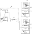
- FIG. 1 is a circuit schematic diagram 1 of a serial communication device provided by the present invention.
- FIG. 2 is a circuit schematic diagram 2 of a serial communication device provided by the present invention.
- FIG. 3 is a circuit schematic diagram 3 of a serial communication device provided by the present invention.
- FIG. 4 is a schematic circuit diagram 4 of a serial communication device provided by the present invention.
- FIG. 5 is a circuit schematic diagram 1 of a serial communication device according to Embodiment 1 of the present invention.
- FIG. 6 is a circuit schematic diagram 2 of a serial communication device according to Embodiment 1 of the present invention.
- FIG. 7 is a circuit schematic diagram 3 of a serial communication device according to Embodiment 1 of the present invention.
- FIG. 8 is a circuit schematic diagram 1 of a serial communication device according to Embodiment 2 of the present invention.
- FIG. 9 is a circuit schematic diagram 2 of a serial communication device according to Embodiment 2 of the present invention.
- FIG. 10 is a circuit principle diagram 3 of a serial communication device according to Embodiment 2 of the present invention.
- FIG. 11 is a circuit schematic diagram 1 of a serial communication device according to Embodiment 3 of the present invention.
- FIG. 12 is a circuit schematic diagram 2 of a serial communication device according to Embodiment 3 of the present invention.
- FIG. 13 is a circuit principle diagram 3 of a serial communication device according to Embodiment 3 of the present invention.
- FIG. 14 is a flowchart of a serial communication method provided by the present invention.
- the serial communication device provided by the present invention is used to meet the requirements of sending control information matched with each chip of the radio frequency front-end module, or to satisfy convenient and fast one-way communication between the chips of the radio frequency front-end module and between the chips.
- the inventor refers to the serial communication device as a SIPI (scalable intraperipheral interface) interface.
- SIPI scalable intraperipheral interface
- the serial communication device provided by the present invention is directly referred to by the SIPI interface.
- the SIPI interface includes a radio frequency front-end module 10 and a radio frequency device 20.
- the first input interface and the second input interface of the radio frequency front-end module 10 are correspondingly connected to the output interface of the main control module.
- Signal bus connection when the first output interface of the radio frequency front-end module 10 is connected to the first input interface of at least one radio frequency device 20 through the first signal bus SA, the second output interface of the radio frequency front-end module 10 is connected through the second signal bus SB It is connected to a second input interface of at least one radio frequency device 20, or at least one second output interface of the radio frequency front-end module 10 is connected to a second input interface of at least one radio frequency device 20 through a second signal bus SB.
- the SIPI interface may also be that at least one first output interface of the radio frequency front-end module 10 is connected to a first input interface of at least one radio frequency device 20 through a first signal bus SA, and at least one of the radio frequency front-end module 10
- the second output interface is connected to the second input interface of the at least one radio frequency device 20 through the second signal bus SB.
- the connection relationship between the first input interface and the second input interface of the radio frequency front-end module 10 is the same as above, and is not repeated here.
- the latest valid SIPI data of the radio frequency device 20 is enabled to generate the first clock signal, otherwise, the system clock signal SCLK and the system data signal SDATA are received again; valid SIPI data is extracted according to the first clock signal sampling and the valid SIPI is set according to a preset rule.
- the data is sent to each radio frequency device 20 in parallel to realize the decoding and configuration of the effective SIPI data (configuration of various uses, such as adjusting current / voltage), so that each radio frequency device 20 can update the effective SIPI data in real time and synchronously.
- the SIPI interface may also be a first output interface of the radio frequency front-end module 10 connected to a first input interface of the first radio frequency device 20 through a first signal bus SA, and a second output interface of the radio frequency front-end module 10. It is connected to the second input interface of the first radio frequency device 20 through the second signal bus SB.
- each radio frequency device 20 is connected in turn through the first signal bus SA and the second signal bus SB (that is, Adjacent radio frequency devices 20 are connected via a first signal bus SA and a second signal bus SB).
- the connection relationship between the first input interface and the second input interface of the radio frequency front-end module 10 is the same as above, and is not repeated here.
- the data is sent one by one (cascaded serial) to each RF device 20 to realize the decoding and configuration of the effective SIPI data (configuration of various uses, such as adjusting current / voltage), so that the RF device 20 sequentially realizes the real-time synchronous update of the effective SIPI. data.
- the structure and principle of the SIPI interface will be described in detail below with reference to FIGS. 5 to 13 and taking the radio frequency front-end module 10 in parallel to transmit the latest valid SIP data to each radio frequency device 20 as an example.
- the method of implementing effective unidirectional transmission of effective SIPI data in parallel it is not difficult to obtain a method of implementing effective unidirectional transmission of effective SIPI data in a cascaded serial manner, and the radio frequency front-end module 10 and each radio frequency using the cascaded serial SIPI interface
- the structure of the device 20 is the same as the structure of the radio frequency front-end module 10 and each radio frequency device 20 using SIPI interfaces in parallel, and details are not described herein again.
- the radio frequency front-end module 10 may include a first detection circuit 100, a first clock generation circuit 102, and a transmission circuit (transmitting circuit TX) 101.
- An input interface and a second input interface are correspondingly connected to the output interface of the main control module (connected through the existing signal bus), and the output interface of the first detection circuit 100 is connected to the first clock generation circuit through one or more clock enable buses
- the input interface of 102 is connected, the output interface of the first clock generation circuit 102 is connected to the first input interface of the transmission circuit 101 (connected through the existing signal bus), and the output interface of the first detection circuit 100 is connected to the second of the transmission circuit 101 Input interface connection.
- the main control module may be any main control chip, baseband chip, etc. having a control function; the first input interface and the second input interface of the first detection circuit 100 (that is, the first input interface and the second input of the radio frequency front-end module 10).
- the interface can be any serial communication device, such as a MIPI interface or a GIPO interface, as long as it can receive the system clock signal SCLK and the system data signal SDATA sent by the main control module.
- the first detection circuit 100 receives the system clock signal SCLK and the system data signal SDATA sent by the main control module, and determines whether there is the latest valid SIPI data of each radio frequency device 20 (effective control information matching each radio frequency device 20); if there is The latest valid SIPI data DATA_S of each radio frequency device 20 controls the first clock generating circuit 102 to generate a first clock signal (SIPI clock signal) of a certain frequency to the sending circuit 101 through the clock enable bus to turn on the clock signal and turn off the clock signal.
- SIPI clock signal SIPI clock signal
- the preset rule may be encoding, sorting, intercepting, and encrypting the valid SIPI data.
- a first power-on reset (Power-on Reset (POR) circuit (not shown in the figure).
- the first power-on reset circuit is connected to the sending circuit 101 and is used to generate a reset signal to reset the sending circuit 101, so that the sending circuit 101 can receive valid SIPI data only after the reset. .
- each radio frequency device 20 When the valid SIPI data received by each radio frequency device 20 includes a clock signal, each radio frequency device 20 includes a second power-on reset (POR) circuit 202, a receiving circuit (receiving circuit RX) 201, and a second power-on
- the reset circuit 202 is connected to the receiving circuit 201 and is used to generate a reset signal to reset the receiving circuit 201, so that the receiving circuit 201 can receive valid SIPI data only after resetting; when the first input interface of the receiving circuit 201 in each radio frequency device 20 is respectively When connected to the first output interface of the transmitting circuit 101 through the first signal bus SA, the second input interface of the receiving circuit 201 in each radio frequency device 20 may be connected to the second output interface of the transmitting circuit 101 through the second signal bus SB, respectively.
- the second input interface of the receiving circuit 201 in each radio frequency device 20 may be connected to the second output interface corresponding to the transmitting circuit 101 through the second signal bus SB; when the first of the receiving circuit 201 in each radio frequency device 20 When the input interface is connected to the first output interface corresponding to the transmitting circuit 101 through the first signal bus SA, the receiving circuit 201 in each radio frequency device 20 Two input interfaces 101 may be a second output is connected to a second signal bus SB to be transmitted through the circuit, respectively.
- the receiving circuit 201 includes a second detection circuit 2010 for sampling and extracting valid SIPI data received by the receiving circuit 201, and realizing decoding and configuration (configuration of various uses) of the valid SIPI data, so that each radio frequency device 20 Real-time synchronization updates valid SIPI data.
- each radio frequency device 20 When the valid SIPI data received by each radio frequency device 20 does not contain a clock signal, each radio frequency device 20 includes a second power-on reset (POR) circuit 202, a receiving circuit (receiving circuit RX) 201, and a second clock
- the generating circuit 203, the second power-on reset circuit 202 is connected to the receiving circuit 201, and its function is the same as above, and will not be repeated;
- the output interface of the receiving circuit 201 is connected to the input of the second clock generating circuit 203 through one or more clock enable buses Interface connection, the output interface of the second clock generating circuit 203 is connected to the input interface of the receiving circuit 201 (connected through the existing signal bus); when the receiving circuit 201 receives valid SIPI data, it will turn on the clock signal through the clock enabling bus And turn off the clock signal to control the second clock generating circuit 203 to generate a second clock signal CLK_i with a certain frequency and send it to the receiving circuit 201.
- POR power-on reset
- the second input interface of the receiving circuit 201 in each radio frequency device 20 may be respectively It is connected to the second output interface of the transmitting circuit 101 through the second signal bus SB; or, the second input interface of the receiving circuit 201 in each radio frequency device 20 may be respectively corresponding to the second output of the transmitting circuit 101 through the second signal bus SB Interface connection; when the first input interface of the receiving circuit 201 in each radio frequency device 20 is connected to the first output interface corresponding to the transmitting circuit 101 through the first signal bus SA, the second of the receiving circuit 201 in each radio frequency device 20 The input interface may be connected to a second output interface corresponding to the transmitting circuit 101 through a second signal bus SB, respectively.
- the receiving circuit 201 includes a second detection circuit 2010 for sampling and extracting valid SIPI data received by the receiving circuit 201 according to the second clock signal CLK_i, so as to decode and configure the valid SIPI data (configure various uses).
- the radio frequency device may be a power amplifier chip / module, a radio frequency switch, a radio frequency chip / module, and the like.
- the radio frequency front-end module 10 may include a first detection circuit 100, a first clock generation circuit 102, and a transmission circuit (transmitting circuit TX) 101; the radio frequency device 20 includes a second Power-on reset (POR) circuit 202, receiving circuit (SIPI receiving circuit RX) 201, the receiving circuit 201 includes a second detection circuit 2010; the first input interface and the second input interface of the first detection circuit 100 Taking the MIPI interface as an example, the connection relationship between the various parts of the SIPI interface provided in this embodiment is as follows: the first input interface CLOCK and the second input interface DATA of the first detection circuit 100 are correspondingly connected to the output interface of the main control module ( (Connected through an existing signal bus), the first detection circuit 100 is connected to an input interface corresponding to the first clock generation circuit 102 through a clock enable bus CLK_ENABLE and a clock enable bus CLK_DISABLE, and an output interface of the first clock generation circuit 102 is passed a
- the second power-on reset circuit 202 generates a reset signal to reset the receiving circuit 201, so that the reset receiving circuit 201 is in a state to receive valid SIPI data; at this time, the system sent by the main control module is received through the first detection circuit 100
- the clock signal SCLK and the system data signal SDATA, and real-time detection and decoding of the received system clock signal SCLK and the system data signal SDATA, and the address information matching the radio frequency device 20 pre-stored in the first detection circuit 100 In order to determine whether there is the latest valid SIPI data of the RF device 20 (effective control information matching each RF device 20); if there is the latest valid SIPI data DATA_S of the RF device 20, the clock enable bus CLK_ENABLE and the clock enable
- the bus CLK_DISABLE corresponds to the open clock signal and the closed clock signal to control the first clock generating circuit 102 to generate a first clock signal (SIPI clock signal) of a certain frequency to the sending circuit 101, and sends the latest valid SIPI data DATA_S
- the sending circuit 101 extracts valid SIPI data according to the first clock signal sample.
- the valid SIPI data is sent to the receiving circuit 201 by means of encoding, sorting, intercepting, and encryption.
- the valid SIPI data received by the receiving circuit 201 includes a clock signal and a data signal. Therefore, the first signal bus SA may be a clock bus. Used for transmitting clock signals; the second signal bus SB may be a data bus for transmitting data signals; and the clock signals and data signals received by the receiving circuit 201 are sampled by the second detection circuit 2010 to extract valid SIPI data, and
- the SIPI data is decoded and configured (configured for various uses), so that the radio frequency device 20 implements real-time synchronization to update valid SIPI data.
- the second detection circuit 2010 can also determine whether the received clock signal and data signal match the radio frequency device.
- the valid SIPI data required by the radio frequency device 20 may be split into a plurality of pieces, and the plurality of receiving circuits 201 may receive the corresponding Multiple valid SIPI data; that is, correspondingly increasing the number of the second output interface DATA of the transmitting circuit 101 and the number of the receiving circuits 201, and the multiple second output interfaces DATA of the transmitting circuit 101 via the corresponding second signal bus SB and the corresponding receiving circuit
- the second input interface DATA of 201 is connected to efficiently and quickly send multiple valid SIPI data (the split multiple valid SIPI data) to the radio frequency device 20 through the multiple second output interfaces DATA of the sending circuit 101.
- each receiving circuit 201 needs to be connected to the second power-on reset circuit 202.
- the second power-on reset circuit 202 generates a reset signal to reset each receiving circuit 201, so that the reset receiving circuit 201 is in Status of valid SIPI data to be received.
- the valid SIPI data DATA [x: 0] required by the radio frequency device 20 is split into valid SIPI data DATA [x: y] and valid SIPI data DATA [y: 0]; then
- the number of the second output interface and the receiving circuit of the transmitting circuit 101 is increased to two, that is, the second output interface of the transmitting circuit 1011 is the second output interface DATA0 and the second output interface DATA1; the receiving circuit is the receiving circuit 201 ′ and The receiving circuit 201 ′′; the second output interface DATA0 is connected to the second input interface DATA of the receiving circuit 201 ′ through the second signal bus SB, and the second output interface DATA1 is connected to the second input interface of the receiving circuit 201 ′′ through the second signal bus SB DATA connection.
- the first output interface CLK of the transmitting circuit 101 is connected to the first input interface CLK of the receiving circuit 201 ′ and the receiving circuit 201 ′′ through the first signal bus SA, respectively.
- a reset signal generated by the second power-on reset circuit 202 resets the receiving circuit 201 ′ and the receiving circuit 201 ′′, respectively, so that the reset receiving circuit 201 ′ and the receiving circuit 201 ′′ are in a state to receive valid SIPI data; at this time,
- the first detection circuit 100 receives the system clock signal SCLK and the system data signal SDATA sent by the main control module, and performs real-time detection and decoding on the received system clock signal SCLK and the system data signal SDATA.
- Pre-stored address information matching the RF device 20 in order to determine whether there is the latest valid SIPI data DATA [x: 0] of the RF device 20; if there is the latest valid SIPI data DATA [x: 0] of the RF device 20, Then, the clock enable bus CLK_ENABLE corresponding to the open clock signal and the closed clock signal is used to control the first clock generating circuit 102 to generate a first clock signal (SIPI clock signal) of a certain frequency to the sending circuit 101, and send the latest valid SIPI data DATA [x: 0] is sent to the sending circuit 101, so that the sending circuit 101 extracts valid SIPI data DATA [x: y] and After the SIPI data DATA [y: 0], the valid SIPI data DATA [x: y] and the valid SIPI data DATA [y: 0] are sent to the receiving circuit 201 ′ and the receiving circuit by coding sorting, interception, encryption, and the like.
- the corresponding valid SIPI data is sampled and extracted by the second detection circuit 2010 of each receiving circuit, so as to decode and configure the extracted valid SIPI data (configure various uses), so that the radio frequency device 20 can achieve real-time synchronous update Valid SIPI data.
- the first output interface and the second output interface of the sending circuit 101 may be used to send the valid SIPI data to each radio frequency device 20. That is, the first input interface of the receiving circuit 201 in each radio frequency device 20 is connected to the first output interface of the transmitting circuit 101 through the first signal bus SA, respectively. The second input interface of the receiving circuit 201 in each radio frequency device 20 can be respectively passed through The second signal bus SB is connected to a second output interface of the transmission circuit 101.
- the reset signal generated by the second power-on reset circuit 202 is used to reset each receiving circuit 201 so that The reset receiving circuit 201 is in a state to receive valid SIPI data; at this time, the first detection circuit 100 receives the system clock signal SCLK and the system data signal SDATA sent by the main control module, and sends the received system clock signal SCLK Real-time detection and decoding with the system data signal SDATA, and the address information that matches the RF device 20 pre-stored in the first detection circuit 100 can be used to determine whether there is the latest valid SIPI data of the RF device 20 DATA [x: 0 ]; If there is the latest valid SIPI data DATA [x: 0] of the radio frequency device 20, the first clock generation circuit 102 is controlled to generate a first clock signal of a certain frequency through the clock enable bus CLK_ENABLE corresponding to the open clock signal and the closed clock signal.
- SIPI clock signal SIPI clock signal
- the sending circuit 101 sends the latest valid SIPI data DATA [x: 0] to the sending circuit 101, so that the sending circuit 101
- the valid SIPI data DATA [x: 0] is encoded, sorted, intercepted, encrypted, etc., and corresponds to the first output interface CLK and the second output interface DATA.
- the corresponding effective SIPI data DATA [x: 0] is sampled and extracted by the second detection circuit 2010 of each receiving circuit, so as to decode and configure the extracted effective SIPI data DATA [x: 0] (Configure various uses), so that the RF device 20 realizes real-time synchronous update of valid SIPI data, and greatly simplifies the serial communication device of all RF devices 20 (the first input interface and the second input interface of the RF device) Complexity.
- the effective SIPI data required by each radio frequency device 20 can be freely and serially allocated in the entire effective SIPI data.
- the radio frequency front-end module 10 may include a first detection circuit 100, a first clock generation circuit 102, and a transmission circuit (SIPI transmission circuit TX) 101; the radio frequency device 20 includes a first Two power-on reset (POR) circuit 202, receiving circuit (SIPI receiving circuit RX) 201, and second clock generating circuit 203; the receiving circuit 201 includes a second detection circuit 2010;
- the MIPI interface is used as an input interface and the second input interface as an example.
- the connection relationship between the various parts of the SIPI interface provided in this embodiment is as follows: the first input interface CLOCK and the second input interface DATA of the first detection circuit 100 and the main The output interface of the control module is connected correspondingly (connected through the existing signal bus).
- the first detection circuit 100 is connected to the input interface corresponding to the first clock generation circuit 102 through the clock enable bus CLK_ENABLE and the clock enable bus CLK_DISABLE.
- the output interface of the generating circuit 102 is connected to the first input interface of the transmitting circuit 101 through the signal bus 104, and the output interface of the first detection circuit 100 is connected to the signal bus 103 through the signal bus 103.
- the second input interface of the transmitting circuit 101 is connected; the first output interface DATA0 of the transmitting circuit 101 is connected to the first input interface DATA0 of the receiving circuit 201 through a first signal bus SA, and the second output interface DATA1 of the transmitting circuit 101 is connected through a second signal
- the bus SB is connected to the second input interface DATA1 of the receiving circuit 201, and the receiving circuit 201 is connected to the second power-on reset circuit 202.
- the second power-on reset circuit 202 generates a reset signal to reset the receiving circuit 201, so that the reset receiving circuit 201 is in a state to receive valid SIPI data; at this time, the system sent by the main control module is received through the first detection circuit 100
- the clock signal SCLK and the system data signal SDATA, and real-time detection and decoding of the received system clock signal SCLK and the system data signal SDATA, and the address information matching the radio frequency device 20 pre-stored in the first detection circuit 100 In order to determine whether there is the latest valid SIPI data of the RF device 20 (effective control information matching each RF device 20); if there is the latest valid SIPI data DATA_S of the RF device 20, the clock enable bus CLK_ENABLE and the clock enable
- the bus CLK_DISABLE corresponds to the open clock signal and the closed clock signal to control the first clock generating circuit 102 to generate a first clock signal (SIPI clock signal) of a certain frequency to the sending circuit 101, and sends the latest valid SIPI data DATA_S
- the sending circuit 101 extracts valid SIPI data according to the first clock signal sample.
- the valid SIPI data is sent to the receiving circuit 201 by means of encoding sorting, interception, encryption, etc .; the valid SIPI data received by the receiving circuit 201 includes only data signals. Therefore, the first signal bus SA may be the first data bus.
- the second signal bus SB may be a second data bus and also used for transmitting data signals; and the data signals transmitted through the first data bus and the data signals transmitted through the second data bus can be sampled from each other Valid SIPI data; since the valid SIPI data includes a data frame header signal, a data signal, and a data frame tail signal, the receiving circuit 201 may pass the data frame header signal or data frame tail signal of the received valid SIPI data and pass The clock enable bus CLK_ENABLE and the clock enable bus CLK_DISABLE correspond to turning on the clock signal and turning off the clock signal to control the second clock generating circuit 203 to generate a second clock signal CLK_i (SIPI clock signal) of a certain frequency to the receiving circuit 201 for the second detection
- the circuit 2010 samples the valid SIPI data according to the second clock signal sampling,
- the data can be decoded efficiently with SIPI configuration (various uses), so that the RF device 20 for real-time synchronous update SIPI valid data.
- the second detection circuit 2010 can also realize whether
- the reset signal generated by the second power-on reset circuit 202 is used to reset each receiving circuit 201 so that the reset The subsequent receiving circuit 201 is in a state to receive valid SIPI data; at this time, the first detection circuit 100 receives the system clock signal SCLK and the system data signal SDATA sent by the main control module, and sends the received system clock signal SCLK and the system The data signal SDATA is detected and decoded in real time, and the address information matched with the RF device 20 pre-stored in the first detection circuit 100 can be used to determine whether there is the latest valid SIPI data DATA [x: 0] of the RF device 20; If there is the latest valid SIPI data DATA [x: 0] of the radio frequency device 20, the first clock generation circuit 102 is controlled to generate a first clock signal of a certain frequency (SIPI) through the clock enable bus CLK_ENABLE corresponding to the open clock signal and the closed clock
- SIPI a certain frequency
- the effective SIPI data DATA [x: 0] is encoded, sorted, intercepted, encrypted, etc., and passed through two sets of data buses (the first data bus DATA0A and the second data
- the bus DATA1A, the first data bus DATA0B, and the second data bus DATA1B) are correspondingly sent to each receiving circuit 201; each receiving circuit 201 may transmit the data frame header signal or data frame tail signal according to the received valid SIPI data, and pass the clock
- the enable bus CLK_ENABLE and the clock enable bus CLK_DISABLE correspond to turning on the clock signal and turning off the clock signal to control the second clock generation circuit 203 to generate a second clock signal CLK_i (SIPI clock signal) of a certain frequency to the receiving circuit 201 so that the second detection circuit
- CLK_i SIPI clock signal
- the transmission circuit 101 may use Unified dual output interface (first output interface and second output interface). For example, as shown in FIG.
- the reset signal generated by the second power-on reset circuit 202 is used to reset each receiving circuit 201 so that The reset receiving circuit 201 is in a state to receive valid SIPI data; at this time, the first detection circuit 100 receives the system clock signal SCLK and the system data signal SDATA sent by the main control module, and sends the received system clock signal SCLK Real-time detection and decoding with the system data signal SDATA, and the address information that matches the RF device 20 pre-stored in the first detection circuit 100 can be used to determine whether there is the latest valid SIPI data of the RF device 20 DATA [x: 0 ]; If there is the latest valid SIPI data DATA [x: 0] of the radio frequency device 20, the first clock generation circuit 102 is controlled to generate a first clock signal of a certain frequency through the clock enable bus CLK_ENABLE corresponding to the open clock signal and the closed clock signal.
- SIPI clock signal SIPI clock signal
- the sending circuit 101 sends the latest valid SIPI data DATA [x: 0] to the sending circuit 101 so that the sending circuit 101 can
- a clock signal is sampled to extract the valid SIPI data DATA [x: 0]
- the valid SIPI data DATA [x: 0] is encoded, sorted, intercepted, encrypted, etc., and corresponds to the first output interface DATA0 and the second output interface DATA1.
- Send to each receiving circuit 201; each receiving circuit 201 can turn on the clock signal and close it by the clock enable bus CLK_ENABLE and the clock enable bus CLK_DISABLE according to the data frame header signal or data frame tail signal of the valid SIPI data received.
- the clock signal is used to control the second clock generating circuit 203 to generate a second clock signal CLK_i (SIPI clock signal) with a certain frequency to the receiving circuit 201, so that the second detection circuit 2010 extracts valid SIPI data according to the second clock signal sampling, and
- the effective SIPI data is decoded and configured (configured for various uses), so that each radio frequency device 20 can update the effective SIPI data in real time and synchronously.
- the valid SIPI data required by the radio frequency device 20 may be split into a plurality of pieces, and the plurality of receiving circuits 201 may receive the corresponding Multiple valid SIPI data; that is, the number of the first output interface DATA0, the second output interface DATA1, and the receiving circuit 201 of the sending circuit 101 is increased correspondingly, and the multiple first output interfaces DATA0 of the sending circuit 101 pass the corresponding first signal bus
- the SA is connected to the first input interface DATA0 of the corresponding receiving circuit 201, and the plurality of second output interfaces DATA1 of the transmitting circuit 101 are connected to the second input interface DATA1 of the corresponding receiving circuit 201 through the corresponding second signal bus SB to realize Through the multiple first output interfaces DATA0 and the second output interface DATA1 of the sending circuit 101, a plurality of valid SIPI data (the split multiple valid SIPI data) are respectively transmitted to a plurality of receiving circuits of the radio frequency device
- Each receiving circuit 201 may enable the bus CLK_ENABLE and the bus CLK_ENABLE according to the received data frame header signal or data frame tail signal of valid SIPI data.
- the clock enable bus CLK_DISABLE corresponds to the open clock signal and the closed clock signal to control the second clock generating circuit 203 to generate a second clock signal CLK_i (SIPI clock signal) of a certain frequency to the receiving circuit 201, so that the second detection circuit 2010 according to the second clock
- the valid SIPI data is decoded and configured (configured for various purposes), so that the radio frequency device 20 can update the valid SIPI data in real time and synchronously.
- each receiving circuit 201 needs to be connected to the second power-on reset circuit 202.
- the second power-on reset circuit 202 generates a reset signal to reset each receiving circuit 201, so that the reset receiving circuit 201 is in Status of valid SIPI data to be received.
- the radio frequency front-end module 10 may include a first detection circuit 100, a first clock generation circuit 102, and a transmission circuit (transmitting circuit TX) 101;
- the radio frequency device 20 includes a second Power-on reset (POR) circuit 202, receiving circuit (SIPI receiving circuit RX) 201, and second clock generating circuit 203;
- the receiving circuit 201 includes a second detection circuit 2010;
- the MIPI interface is used as an input interface and the second input interface as an example.
- the connection relationship between the various parts of the SIPI interface provided in this embodiment is as follows: the first input interface CLOCK and the second input interface DATA of the first detection circuit 100 and the main The output interface of the control module is connected correspondingly (connected through the existing signal bus).
- the first detection circuit 100 is connected to the input interface corresponding to the first clock generation circuit 102 through the clock enable bus CLK_ENABLE and the clock enable bus CLK_DISABLE.
- the output interface of the generating circuit 102 is connected to the first input interface of the transmitting circuit 101 through the signal bus 104, and the output interface of the first detection circuit 100 is connected to the first input interface of the transmitting circuit 101 through the signal bus 103.
- the second input interface of the transmitting circuit 101 is connected; the first output interface DATA of the transmitting circuit 101 is connected to the first input interface DATA of the receiving circuit 201 through a first signal bus SA, and the second output interface SE of the transmitting circuit 101 is connected through a second signal
- the bus SB is connected to the second input interface SE of the receiving circuit 201, and the receiving circuit 201 is connected to the second power-on reset circuit 202.
- the second power-on reset circuit 202 generates a reset signal to reset the receiving circuit 201, so that the reset receiving circuit 201 is in a state to receive valid SIPI data; at this time, the system sent by the main control module is received through the first detection circuit 100
- the clock signal SCLK and the system data signal SDATA, and real-time detection and decoding of the received system clock signal SCLK and the system data signal SDATA, and the address information matching the radio frequency device 20 pre-stored in the first detection circuit 100 In order to determine whether there is the latest valid SIPI data of the RF device 20 (effective control information matching each RF device 20); if there is the latest valid SIPI data DATA_S of the RF device 20, the clock enable bus CLK_ENABLE and the clock enable
- the bus CLK_DISABLE corresponds to the open clock signal and the closed clock signal to control the first clock generating circuit 102 to generate a first clock signal (SIPI clock signal) of a certain frequency to the sending circuit 101, and sends the latest valid SIPI data DATA_S
- the sending circuit 101 extracts valid SIPI data according to the first clock signal sample.
- the effective SIPI data is sent to the receiving circuit 201 by means of encoding, sorting, intercepting, and encryption.
- the effective SIPI data received by the receiving circuit 201 includes a data signal and an enable signal.
- the first signal bus SA may be data The bus is used for transmitting data signals; the second signal bus SB may be an enable bus and also used for transmitting an enable signal; and the data signal transmitted by the data bus and the enable signal transmitted by the enable bus can be mutually sampled to be effective SIPI data; since the valid SIPI data includes a data frame header signal, a data signal, and a data frame trailer signal, the receiving circuit 201 may pass the clock according to the received data frame header signal or data frame trailer signal of the valid SIPI data, and pass the clock.
- the enable bus CLK_ENABLE and the clock enable bus CLK_DISABLE correspond to turning on the clock signal and turning off the clock signal to control the second clock generation circuit 203 to generate a second clock signal CLK_i (SIPI clock signal) of a certain frequency to the receiving circuit 201 so that the second detection circuit After extracting valid SIPI data according to the second clock signal sampling, and then valid SIP I data is decoded and configured (configured for various uses), so that the radio frequency device 20 implements real-time synchronization to update valid SIPI data.
- the second detection circuit 2010 can also determine whether the received data signal matches the radio frequency device; the data frame header signal and the data frame tail signal are respectively used to determine the start and end positions of the data bits of the valid SIPI data.
- the valid SIPI data required by the radio frequency device 20 may be split into a plurality of pieces, and the plurality of receiving circuits 201 may receive the corresponding Multiple valid SIPI data; that is, correspondingly increasing the number of the second output interface SE of the sending circuit 101 and the receiving circuit 201, and the multiple second output interfaces SE of the sending circuit 101 through the corresponding second signal bus SB and the corresponding receiving circuit
- the second input interface SE of 201 is connected so as to efficiently and quickly send multiple valid SIPI data (the split multiple valid SIPI data) to the radio frequency device 20 through the multiple second output interfaces SE of the sending circuit 101.
- each receiving circuit 201 can turn on the clock signal and close it correspondingly through the clock enable bus CLK_ENABLE and the clock enable bus CLK_DISABLE according to the data frame header signal or data frame tail signal of the valid SIPI data received.
- a second clock extraction circuit 2010 efficient SIPI sampled data signal, and decodes the configuration (various uses) the SIPI valid data, so that the RF device 20 to achieve an effective real-time synchronization SIPI updated data.
- each receiving circuit 201 needs to be connected to the second power-on reset circuit 202.
- the second power-on reset circuit 202 generates a reset signal to reset each receiving circuit 201, so that the reset receiving circuit 201 is in Status of valid SIPI data to be received.
- the valid SIPI data DATA [x: 0] required by the radio frequency device 20 is split into valid SIPI data DATA [x: y] and valid SIPI data DATA [y: 0]; then
- the number of the second output interface and the receiving circuit of the sending circuit 101 is increased to two, that is, the second output interface of the sending circuit 1011 is the second output interface SE0 and the second output interface SE1; the receiving circuit is the receiving circuit 201 ′ and The receiving circuit 201 ′′;
- the second output interface SE0 is connected to the second input interface SE0 of the receiving circuit 201 ′ through the second signal bus SB, and the second output interface SE1 is connected to the second input interface of the receiving circuit 201 ′′ through the second signal bus SB SE1 is connected, and the first output interface DATA of the transmitting circuit 101 is connected to the first input interface DATA of the receiving circuit 201 ′ and the receiving circuit 201 ′′ through the first signal bus SA, respectively.
- a reset signal generated by the second power-on reset circuit 202 resets the receiving circuit 201 ′ and the receiving circuit 201 ′′, respectively, so that the reset receiving circuit 201 ′ and the receiving circuit 201 ′′ are in a state to receive valid SIPI data; at this time,
- the first detection circuit 100 receives the system clock signal SCLK and the system data signal SDATA sent by the main control module, and performs real-time detection and decoding on the received system clock signal SCLK and the system data signal SDATA.
- Pre-stored address information matching the RF device 20 in order to determine whether there is the latest valid SIPI data DATA [x: 0] of the RF device 20; if there is the latest valid SIPI data DATA [x: 0] of the RF device 20, Then, the clock enable bus CLK_ENABLE corresponding to the open clock signal and the closed clock signal is used to control the first clock generating circuit 102 to generate a first clock signal (SIPI clock signal) of a certain frequency to the sending circuit 101, and send the latest valid SIPI data DATA [x: 0] is sent to the sending circuit 101, so that the sending circuit 101 extracts valid SIPI data DATA [x: y] and After validating the SIPI data DATA [y: 0], the valid SIPI data DATA [x: y] and the valid SIPI data DATA [y: 0] are sent to the receiving circuit 201 ′ and received correspondingly by encoding sorting, interception, and encryption.
- SIPI clock signal a first clock signal
- the circuit 201 ′′; the receiving circuit 201 ′ and the receiving circuit 201 ′′ may turn on the clock signal according to the received data frame header signal or data frame tail signal of the valid SIPI data, and correspondingly enable the clock enable bus CLK_ENABLE and the clock enable bus CLK_DISABLE.
- the transmission circuit 101 may use Unified dual output interface (first output interface DATA and second output interface SE). For example, as shown in FIG.
- the reset signal generated by the second power-on reset circuit 202 is used to reset each receiving circuit 201 so that The reset receiving circuit 201 is in a state to receive valid SIPI data; at this time, the first detection circuit 100 receives the system clock signal SCLK and the system data signal SDATA sent by the main control module, and sends the received system clock signal SCLK Real-time detection and decoding with the system data signal SDATA, and the address information that matches the RF device 20 pre-stored in the first detection circuit 100 can be used to determine whether there is the latest valid SIPI data of the RF device 20 DATA [x: 0 ]; If there is the latest valid SIPI data DATA [x: 0] of the radio frequency device 20, the first clock generation circuit 102 is controlled to generate a first clock signal of a certain frequency through the clock enable bus CLK_ENABLE corresponding to the open clock signal and the closed clock signal.
- SIPI clock signal SIPI clock signal
- the sending circuit 101 sends the latest valid SIPI data DATA [x: 0] to the sending circuit 101 so that the sending circuit 101 can
- a clock signal is sampled to extract the valid SIPI data DATA [x: 0]
- the valid SIPI data DATA [x: 0] is encoded, sorted, intercepted, encrypted, etc., and corresponds to the first output interface DATA and the second output interface SE.
- Send to each receiving circuit 201; each receiving circuit 201 can turn on the clock signal and close it by the clock enable bus CLK_ENABLE and the clock enable bus CLK_DISABLE according to the data frame header signal or data frame tail signal of the valid SIPI data received.
- the clock signal is used to control the second clock generating circuit 203 to generate a second clock signal CLK_i (SIPI clock signal) with a certain frequency to the receiving circuit 201, so that the second detection circuit 2010 extracts valid SIPI data according to the second clock signal sampling, and
- the effective SIPI data is decoded and configured (configured for various uses), so that each radio frequency device 20 can update the effective SIPI data in real time and synchronously.
- the serial communication device detects and extracts valid SIPI data required by each radio frequency device through a radio frequency front-end module, and sends the valid SIPI data quickly and efficiently in a parallel or cascaded serial manner. For each radio frequency device, it can meet the needs of convenient and fast unidirectional communication between the chips of the radio frequency front-end module and between the chips, while reducing the communication complexity and having higher transmission efficiency.
- the present invention also provides a serial communication method. As shown in FIG. 14, the serial communication method includes the following steps:
- Step S1 judging whether the received system clock signal and system data signal have the latest valid SIPI data through the radio frequency front-end module;
- Step S2 if there is the latest valid SIPI data, enable the generation of the first clock signal; otherwise, receive the system clock signal and the system data signal again;
- Step S3 the radio frequency front-end module extracts valid SIPI data according to the first clock signal sampling, and sends the valid SIPI data to each radio frequency device in parallel or serially according to a preset rule;
- Step S4 if the valid SIPI data received by each radio frequency device includes a clock signal, decode and configure the valid SIPI data; otherwise, enable the generation of a second clock signal and extract the valid SIPI data according to the second clock signal sampling Perform decoding and configuration.
- the serial communication device provided by the present invention can be used in a semiconductor device (such as a radio frequency chip or a radio frequency module) for satisfying sending control information matching the semiconductor device to the semiconductor device, or for satisfying each semiconductor device and within the semiconductor device. Convenient and fast one-way communication needs. The specific structure of the semiconductor device will not be described in detail here.
Landscapes
- Engineering & Computer Science (AREA)
- Theoretical Computer Science (AREA)
- Physics & Mathematics (AREA)
- General Engineering & Computer Science (AREA)
- General Physics & Mathematics (AREA)
- Computer Networks & Wireless Communication (AREA)
- Signal Processing (AREA)
- Telephone Function (AREA)
- Transceivers (AREA)
- Mobile Radio Communication Systems (AREA)
- Synchronisation In Digital Transmission Systems (AREA)
Abstract
本发明公开了一种串行通信装置及串行通信方法。该串行通信装置包括射频前端模块和射频器件,射频前端模块的第一输入接口和第二输入接口与主控模块的输出接口对应连接,射频前端模块的第一输出接口通过第一信号总线与至少一个射频器件的第一输入接口连接时,射频前端模块的第二输出接口通过第二信号总线与至少一个射频器件的第二输入接口连接。本发明可以满足射频前端模块的各个芯片之间以及芯片内部之间便捷、快速的单向通信需求,同时还降低了通信复杂度,具有更高的传输效率。
Description
本发明涉及一种串行通信装置,同时也涉及相应的串行通信方法。
随着射频前端(RF Front-end)的应用越来越复杂,所需要的功率放大器、射频开关、低噪声功率放大器、滤波器等芯片的数量也越来越多。那么,射频前端模块的各个芯片都需要通过各自的控制信号来切换在实际应用中的状态。对于各个芯片的状态不是太多的情况,现有技术中普遍采用GPIO(General purpose input output)接口,通过高电平“1”和低电平“0”的状态组合来控制各个芯片的状态变化。
但是,随着射频前端的应用日益复杂和功能不断增多,每个芯片的功能也越来越多,进一步增加GPIO控制信号线的数量是不现实的。因此,在手机领域出现了MIPI(Mobile Industry Processor Interface)接口,然而在成本压力日益提高的情况下,射频前端模块内部的芯片之间相互通信采用MIPI接口反而会增加芯片复杂度,从而降低内部通信的效率。
发明内容
针对现有技术的不足,本发明所要解决的首要技术问题在于提供一种串行通信装置。
本发明所要解决的另一技术问题在于提供一种串行通信方法。
本发明所要解决的又一技术问题在于提供一种包括上述串行通信装置的半导体器件。
为了实现上述目的,本发明采用下述的技术方案:
根据本发明实施例的第一方面,提供一种串行通信装置,包括射频前端模块和射频器件,所述射频前端模块的第一输入接口和第二输入接口与主控模块的输出接口对应连接,所述射频前端模块的第一输出接口通过第一信号总线与至少一个所述射频器件的第一输入接口连接时,所述射频前端模块的第二输出接口通过第二信号总线与至少一 个所述射频器件的第二输入接口连接。
根据本发明实施例的第二方面,提供一种串行通信装置,包括射频前端模块和射频器件,所述射频前端模块的第一输入接口和第二输入接口与主控模块的输出接口对应连接,所述射频前端模块的至少一个第一输出接口通过第一信号总线与至少一个所述射频器件的第一输入接口连接,所述射频前端模块的至少一个第二输出接口通过第二信号总线与至少一个所述射频器件的第二输入接口连接。
根据本发明实施例的第三方面,提供一种串行通信装置,包括射频前端模块和射频器件,所述射频前端模块的第一输入接口和第二输入接口与主控模块的输出接口对应连接,所述射频前端模块的第一输出接口通过第一信号总线与首个所述射频器件的第一输入接口连接,所述射频前端模块的第二输出接口通过第二信号总线与首个所述射频器件的第二输入接口连接,从首个所述射频器件开始,各所述射频器件之间依次分别通过第一信号总线和第二信号总线连接。
其中较优地,所述射频前端模块包括第一检测电路、第一时钟产生电路及发送电路,所述第一检测电路的第一输入接口和第二输入接口与所述主控模块的输出接口对应连接,所述第一检测电路的输出接口通过一根或多根时钟使能总线与所述第一时钟产生电路的输入接口连接,所述第一时钟产生电路的输出接口与所述发送电路的第一输入接口连接,所述第一检测电路的输出接口与所述发送电路的第二输入接口连接。
其中较优地,所述第一输入接口和所述第二输入接口包括但不限于MIPI接口或GIPO接口。
其中较优地,所述射频前端模块还包括第一上电复位电路,所述第一上电复位电路与所述发送电路连接。
其中较优地,当各所述射频器件接收的有效SIPI数据中含有时钟信号时,所述射频器件包括第二上电复位电路、接收电路,所述第二上电复位电路与所述接收电路连接,所述接收电路的第一输入接口通过所述第一信号总线与发送电路的第一输出接口连接时,所述接收电路的第二输入接口分别通过所述第二信号总线与所述发送电路的第二输出接口连接,或者,所述接收电路的第二输入接口通过所述第二信 号总线与所述发送电路对应的第二输出接口连接。
其中较优地,当各所述射频器件接收的有效SIPI数据中含有时钟信号时,所述射频器件包括第二上电复位电路、接收电路,所述第二上电复位电路与所述接收电路连接,所述接收电路的第一输入接口通过所述第一信号总线与发送电路对应的第一输出接口连接,所述接收电路的第二输入接口通过第二信号总线与所述发送电路对应的第二输出接口连接。
其中较优地,当各所述射频器件接收的有效SIPI数据中含有时钟信号时,所述射频器件包括第二上电复位电路、接收电路,所述第二上电复位电路与所述接收电路连接,首个所述射频器件的接收电路的第一输入接口通过所述第一信号总线与发送电路的第一输出接口连接,首个所述射频器件的接收电路的第二输入接口通过所述第二信号总线与发送电路的第二输出接口连接,从首个所述射频器件开始,各所述射频器件的接收电路之间依次分别通过第一信号总线和第二信号总线连接。
其中较优地,根据每个所述射频器件所需的有效SIPI数据的数据位宽,调整所述发送电路的第二输出接口及每个所述射频器件的接收电路的数量。
其中较优地,当各所述射频器件接收的有效SIPI数据中不含有时钟信号时,所述射频器件包括第二上电复位电路、接收电路及第二时钟产生电路,所述第二上电复位电路与所述接收电路连接,所述接收电路的输出接口通过一根或多根时钟使能总线与所述第二时钟产生电路的输入接口连接,所述第二时钟产生电路的输出接口与所述接收电路的输入接口连接,所述接收电路的第一输入接口通过所述第一信号总线与发送电路的第一输出接口连接时,所述接收电路的第二输入接口分别通过所述第二信号总线与所述发送电路的第二输出接口连接,或者,所述接收电路的第二输入接口通过所述第二信号总线与所述发送电路对应的第二输出接口连接。
其中较优地,当各所述射频器件接收的有效SIPI数据中不含有时钟信号时,所述射频器件包括第二上电复位电路、接收电路及第二时钟产生电路,所述第二上电复位电路与所述接收电路连接,所述接收 电路的输出接口通过一根或多根时钟使能总线与所述第二时钟产生电路的输入接口连接,所述第二时钟产生电路的输出接口与所述接收电路的输入接口连接,所述接收电路的第一输入接口通过所述第一信号总线与发送电路对应的第一输出接口连接,所述接收电路的第二输入接口通过第二信号总线与所述发送电路对应的第二输出接口连接。
其中较优地,当各所述射频器件接收的有效SIPI数据中不含有时钟信号时,所述射频器件包括第二上电复位电路、接收电路及第二时钟产生电路,所述第二上电复位电路与所述接收电路连接,所述接收电路的输出接口通过一根或多根时钟使能总线与所述第二时钟产生电路的输入接口连接,所述第二时钟产生电路的输出接口与所述接收电路的输入接口连接,首个所述射频器件的接收电路的第一输入接口通过所述第一信号总线与发送电路的第一输出接口连接,首个所述射频器件的接收电路的第二输入接口通过所述第二信号总线与发送电路的第二输出接口连接,从首个所述射频器件开始,各所述射频器件的接收电路之间依次分别通过第一信号总线和第二信号总线连接。
其中较优地,根据每个所述射频器件所需的有效SIPI数据的数据位宽,调整所述发送电路的第一输出接口、第二输出接口及每个所述射频器件的接收电路的数量。
其中较优地,根据每个所述射频器件所需的有效SIPI数据的数据位宽,调整所述发送电路的第二输出接口及每个所述射频器件的接收电路的数量。
其中较优地,所述接收电路包括第二检测电路,用于将所述接收电路接收的有效SIPI数据进行采样提取,实现对有效SIPI数据的解码与配置。
根据本发明实施例的第四方面,提供一种串行通信方法,包括如下步骤:
通过射频前端模块判断所接收的系统时钟信号和系统数据信号中是否有最新的有效SIPI数据;
如果有最新的有效SIPI数据,则使能产生第一时钟信号;否则重新接收系统时钟信号和系统数据信号;
射频前端模块根据第一时钟信号提取有效SIPI数据,并按照预设规 则将该有效SIPI数据并行或串行发送到各射频器件中;
如果各射频器件所接收的有效SIPI数据包含有时钟信号,则对有效SIPI数据进行解码与配置;否则,使能产生第二时钟信号,并根据该第二时钟信号提取有效SIPI数据进行解码与配置。
根据本发明实施例的第五方面,提供一种半导体器件,该半导体芯片中包括上述的串行通信装置。
本发明所提供的串行通信装置,通过射频前端模块实施侦测并提取出各射频器件所需的有效SIPI数据,并以并行或级联串行的方式将该有效SIPI数据快速、高效地发送给各射频器件,可以满足射频前端模块的各个芯片之间以及芯片内部之间便捷、快速的单向通信需求,同时还降低了通信复杂度,具有更高的传输效率。
图1为本发明所提供的串行通信装置的电路原理图1;
图2为本发明所提供的串行通信装置的电路原理图2;
图3为本发明所提供的串行通信装置的电路原理图3;
图4为本发明所提供的串行通信装置的电路原理图4;
图5为本发明实施例1所提供的串行通信装置的电路原理图1;
图6为本发明实施例1所提供的串行通信装置的电路原理图2;
图7为本发明实施例1所提供的串行通信装置的电路原理图3;
图8为本发明实施例2所提供的串行通信装置的电路原理图1;
图9为本发明实施例2所提供的串行通信装置的电路原理图2;
图10为本发明实施例2所提供的串行通信装置的电路原理图3;
图11为本发明实施例3所提供的串行通信装置的电路原理图1;
图12为本发明实施例3所提供的串行通信装置的电路原理图2;
图13为本发明实施例3所提供的串行通信装置的电路原理图3;
图14为本发明所提供的串行通信方法的流程图。
下面结合附图和具体实施例对本发明的技术内容做进一步的详细说明。
本发明所提供的串行通信装置用于满足向射频前端模块的各个芯片发送与其匹配的控制信息,或者满足射频前端模块的各个芯片之间 以及芯片内部之间便捷、快速的单向通信需求。为了便于描述,发明人将该串行通信装置称为SIPI(scalable intra peripheral interface)接口。在本发明中,将以SIPI接口直接指代本发明所提供的串行通信装置。
如图1和图2所示,本SIPI接口包括射频前端模块10和射频器件20,射频前端模块10的第一输入接口和第二输入接口与主控模块的输出接口对应连接(可以通过现有的信号总线连接),射频前端模块10的第一输出接口通过第一信号总线SA与至少一个射频器件20的第一输入接口连接时,射频前端模块10的第二输出接口通过第二信号总线SB与至少一个射频器件20的第二输入接口连接,或者,射频前端模块10的至少一个第二输出接口通过第二信号总线SB与至少一个射频器件20的第二输入接口连接。
如图3所示,本SIPI接口还可以是由射频前端模块10的至少一个第一输出接口通过第一信号总线SA与至少一个射频器件20的第一输入接口连接,射频前端模块10的至少一个第二输出接口通过第二信号总线SB与至少一个射频器件20的第二输入接口连接;其中,射频前端模块10的第一输入接口和第二输入接口的连接关系同上,在此不再赘述。
通过射频前端模块10接收主控模块发送的系统时钟信号SCLK和系统数据信号SDATA,判断是否有各射频器件20最新的有效SIPI数据(与各射频器件20相匹配的有效控制信息);如果有各射频器件20最新的有效SIPI数据,则使能产生第一时钟信号,否则重新接收系统时钟信号SCLK和系统数据信号SDATA;根据第一时钟信号采样提取有效SIPI数据并按照预设规则将该有效SIPI数据并行发送到各射频器件20中,实现对有效SIPI数据的解码与配置(配置各项用途,如调整电流/电压),从而使得各射频器件20实现实时同步更新有效SIPI数据。
如图4所示,本SIPI接口还可以是由射频前端模块10的第一输出接口通过第一信号总线SA与首个射频器件20的第一输入接口连接,射频前端模块10的第二输出接口通过第二信号总线SB与首个射频器件20的第二输入接口连接,从首个射频器件20开始,各射频器件20 之间依次分别通过第一信号总线SA和第二信号总线SB连接(即相邻射频器件20之间通过第一信号总线SA和第二信号总线SB连接);其中,射频前端模块10的第一输入接口和第二输入接口的连接关系同上,在此不再赘述。
通过射频前端模块10接收主控模块发送的系统时钟信号SCLK和系统数据信号SDATA,判断是否有各射频器件20最新的有效SIPI数据(与各射频器件20相匹配的有效控制信息);如果有各射频器件20最新的有效SIPI数据,则使能产生第一时钟信号,否则重新接收系统时钟信号SCLK和系统数据信号SDATA;根据第一时钟信号采样提取有效SIPI数据并按照预设规则将该有效SIPI数据逐个发送(级联串行)到各射频器件20中,实现对有效SIPI数据的解码与配置(配置各项用途,如调整电流/电压),从而使得射频器件20依次实现实时同步更新有效SIPI数据。
下面结合图5~图13,并以射频前端模块10采用并行方式向各射频器件20传输最新的有效SIP数据为例,对本SIPI接口的结构和原理进行详细说明。根据采用并行方式实现单向传输有效SIPI数据的方法不难得到采用级联串行方式实现单向传输有效SIPI数据的方法,并且采用级联串行方式的SIPI接口的射频前端模块10和各射频器件20的结构与采用并行方式的SIPI接口的射频前端模块10和各射频器件20的结构相同,在此就不再赘述了。
如图5~图13所示,在本SIPI接口中,射频前端模块10可以包括第一检测电路100、第一时钟产生电路102及发送电路(发送电路TX)101,第一检测电路100的第一输入接口和第二输入接口与主控模块的输出接口对应连接(通过现有的信号总线连接),第一检测电路100输出接口通过一根或多根时钟使能总线与第一时钟产生电路102的输入接口连接,第一时钟产生电路102的输出接口与发送电路101的第一输入接口连接(通过现有的信号总线连接),第一检测电路100的输出接口与发送电路101的第二输入接口连接。其中,主控模块可以是任何具有控制功能的主控芯片、基带芯片等;第一检测电路100的第一输入接口和第二输入接口(即射频前端模块10的第一输入接口和第二输入接口)可以是任何串行通信装置,例如MIPI接口或GIPO 接口,只要能接收主控模块发送的系统时钟信号SCLK和系统数据信号SDATA即可。
通过第一检测电路100接收主控模块发送的系统时钟信号SCLK和系统数据信号SDATA,判断是否有各射频器件20最新的有效SIPI数据(与各射频器件20相匹配的有效控制信息);如果有各射频器件20最新的有效SIPI数据DATA_S,则通过时钟使能总线打开时钟信号和关闭时钟信号来控制第一时钟产生电路102产生一定频率的第一时钟信号(SIPI时钟信号)给发送电路101,并将该最新的有效SIPI数据DATA_S发送给发送电路101,以便发送电路101根据第一时钟信号采样提取有效SIPI数据后,将该有效SIPI数据按照预设规则发送到各射频器件20中;其中,预设规则可以是对有效SIPI数据进行编码排序、截取、加密等。
为了确定射频前端模块10的发送电路101是否处于稳态,以保证该发送电路101每次接收的有效SIPI数据DATA_S的准确性,可以在射频前端模块10中设置第一上电复位(Power-on Reset,POR)电路(图中未示出),第一上电复位电路与发送电路101连接,用于产生复位信号去复位发送电路101,从而使得发送电路101经复位后才能接收有效SIPI数据DATA_S。
当各射频器件20接收的有效SIPI数据中含有时钟信号时,各射频器件20包括第二上电复位(Power-on Reset,POR)电路202、接收电路(接收电路RX)201,第二上电复位电路202与接收电路201连接,用于产生复位信号去复位接收电路201,从而使得接收电路201经复位后才能接收有效SIPI数据;当各射频器件20中的接收电路201的第一输入接口分别通过第一信号总线SA与发送电路101的第一输出接口连接时,各射频器件20中的接收电路201的第二输入接口可以分别通过第二信号总线SB与发送电路101的第二输出接口连接;或者,各射频器件20中的接收电路201的第二输入接口可以分别通过第二信号总线SB与发送电路101对应的第二输出接口连接;当各射频器件20中的接收电路201的第一输入接口分别通过第一信号总线SA与发送电路101对应的第一输出接口连接时,各射频器件20中的接收电路201的第二输入接口可以分别通过第二信号总线SB与发送电路101对 应的第二输出接口连接。其中,接收电路201包括第二检测电路2010,用于将接收电路201接收的有效SIPI数据进行采样提取,实现对该有效SIPI数据的解码与配置(配置各种用途),从而使得各射频器件20实现实时同步更新有效SIPI数据。
当各射频器件20接收的有效SIPI数据中不含有时钟信号时,各射频器件20包括第二上电复位(Power-on Reset,POR)电路202、接收电路(接收电路RX)201及第二时钟产生电路203,第二上电复位电路202与接收电路201连接,其作用同上,不再赘述;接收电路201的输出接口通过一根或多根时钟使能总线与第二时钟产生电路203的输入接口连接,第二时钟产生电路203的输出接口与接收电路201的输入接口连接(通过现有的信号总线连接);当接收电路201接收到有效SIPI数据后,会通过时钟使能总线打开时钟信号和关闭时钟信号来控制第二时钟产生电路203产生一定频率的第二时钟信号CLK_i发给接收电路201。当各射频器件20中的接收电路201的第一输入接口分别通过第一信号总线SA与发送电路101的第一输出接口连接时,各射频器件20中的接收电路201的第二输入接口可以分别通过第二信号总线SB与发送电路101的第二输出接口连接;或者,各射频器件20中的接收电路201的第二输入接口可以分别通过第二信号总线SB与发送电路101对应的第二输出接口连接;当各射频器件20中的接收电路201的第一输入接口分别通过第一信号总线SA与发送电路101对应的第一输出接口连接时,各射频器件20中的接收电路201的第二输入接口可以分别通过第二信号总线SB与发送电路101对应的第二输出接口连接。其中,接收电路201包括第二检测电路2010,用于根据第二时钟信号CLK_i将接收电路201接收的有效SIPI数据进行采样提取,实现对该有效SIPI数据的解码与配置(配置各种用途)。其中,射频器件可以是功放芯片/模块、射频开关、射频芯片/模块等。
下面,分别以射频器件20的数量为1个和2个为例,并结合图5~图16,对上述的SIPI接口的结构和原理进行详细说明。
实施例1
如图5所示,本实施例所提供的SIPI接口中,射频前端模块10可以包括第一检测电路100、第一时钟产生电路102及发送电路(发 送电路TX)101;射频器件20包括第二上电复位(Power-on Reset,POR)电路202、接收电路(SIPI接收电路RX)201,接收电路201包括第二检测电路2010;以第一检测电路100的第一输入接口和第二输入接口采用MIPI接口为例,本实施例所提供的SIPI接口各部分之间的连接关系如下:第一检测电路100的第一输入接口CLOCK和第二输入接口DATA与主控模块的输出接口对应连接(通过现有的信号总线连接),第一检测电路100通过时钟使能总线CLK_ENABLE和时钟使能总线CLK_DISABLE与第一时钟产生电路102对应的输入接口连接,第一时钟产生电路102的输出接口通过信号总线104与发送电路101的第一输入接口连接,第一检测电路100的输出接口通过信号总线103与发送电路101的第二输入接口连接;发送电路101的第一输出接口CLK通过第一信号总线SA与接收电路201的第一输入接口CLK连接,发送电路101的第二输出接口DATA通过第二信号总线SB与接收电路201的第二输入接口DATA连接,接收电路201与第二上电复位电路202连接。
通过第二上电复位电路202产生复位信号去复位接收电路201,使得经复位后的接收电路201处于待接收有效SIPI数据的状态;此时,通过第一检测电路100接收主控模块发送的系统时钟信号SCLK和系统数据信号SDATA,并将所接收的系统时钟信号SCLK和系统数据信号SDATA进行实时侦测解码,并可以通过第一检测电路100中预存的与射频器件20相匹配的地址信息,以实现判断是否有射频器件20最新的有效SIPI数据(与各射频器件20相匹配的有效控制信息);如果有射频器件20最新的有效SIPI数据DATA_S,则通过时钟使能总线CLK_ENABLE和时钟使能总线CLK_DISABLE对应打开时钟信号和关闭时钟信号来控制第一时钟产生电路102产生一定频率的第一时钟信号(SIPI时钟信号)给发送电路101,并将该最新的有效SIPI数据DATA_S发送给发送电路101,以便发送电路101根据第一时钟信号采样提取有效SIPI数据后,将该有效SIPI数据采用编码排序、截取、加密等方式发送到接收电路201;其中,接收电路201接收的有效SIPI数据包括时钟信号和数据信号,因此,第一信号总线SA可以为时钟总线,用于传输时钟信号;第二信号总线SB可以为数据总线,用于传输数据 信号;并且接收电路201接收的时钟信号和数据信号通过第二检测电路2010采样提取出有效SIPI数据,并对该有效SIPI数据进行解码与配置(配置各种用途),从而使得射频器件20实现实时同步更新有效SIPI数据。其中,第二检测电路2010还可以实现判断所接收的时钟信号和数据信号是否与本射频器件相匹配。
当本实施例的射频器件20所需的有效SIPI数据的数据位宽较长时,可以将该射频器件20所需的有效SIPI数据拆分成多个,并通过多个接收电路201对应接收该多个有效SIPI数据;即相应的增加发送电路101的第二输出接口DATA及接收电路201的数量,发送电路101的多个第二输出接口DATA通过相应的第二信号总线SB与对应的接收电路201的第二输入接口DATA连接,以实现通过发送电路101的多个第二输出接口DATA高效快速的将多个有效SIPI数据(所拆分的多个有效SIPI数据)分别对应发送给射频器件20的多个接收电路201,并通过各接收电路201的第二检测电路2010采样提取出对应的有效SIPI数据,对所提取的有效SIPI数据进行解码与配置(配置各种用途),从而使得射频器件20实现实时同步更新有效SIPI数据。需要强调的是,每个接收电路201都需要与第二上电复位电路202连接,通过第二上电复位电路202产生复位信号去复位每个接收电路201,使得经复位后的接收电路201处于待接收有效SIPI数据的状态。
例如,如图6所示,假设本射频器件20所需的有效SIPI数据DATA[x:0]被拆分成有效SIPI数据DATA[x:y]和有效SIPI数据DATA[y:0];那么,发送电路101的第二输出接口和接收电路的数量分别增加至两个,即发送电路1011的第二输出接口为第二输出接口DATA0和第二输出接口DATA1;接收电路为接收电路201′和接收电路201″;第二输出接口DATA0通过第二信号总线SB与接收电路201′的第二输入接口DATA连接,第二输出接口DATA1通过第二信号总线SB与接收电路201″的第二输入接口DATA连接,发送电路101的第一输出接口CLK通过第一信号总线SA分别与接收电路201′和接收电路201″的第一输入接口CLK连接。
通过第二上电复位电路202产生复位信号分别去复位接收电路201′和接收电路201″,使得经复位后的接收电路201′和接收电路201″处于待接收有效SIPI数据的状态;此时,通过第一检测电路100接收主控模块发送的系统时钟信号SCLK和系统数据信号SDATA,并将所接收的系统时钟信号SCLK和系统数据信号SDATA进行实时侦测解码,并可以通过第一检测电路100中预存的与射频器件20相匹配的地址信息,以实现判断是否有射频器件20最新的有效SIPI数据DATA[x:0];如果有射频器件20最新的有效SIPI数据DATA[x:0],则通过时钟使能总线CLK_ENABLE对应打开时钟信号和关闭时钟信号来控制第一时钟产生电路102产生一定频率的第一时钟信号(SIPI时钟信号)给发送电路101,并将该最新的有效SIPI数据DATA[x:0]发送给发送电路101,以便发送电路101根据第一时钟信号采样提取有效SIPI数据DATA[x:y]和有效SIPI数据DATA[y:0]后,将该有效SIPI数据DATA[x:y]和有效SIPI数据DATA[y:0]采用编码排序、截取、加密等方式对应发送到接收电路201′和接收电路201″;通过各接收电路的第二检测电路2010采样提取出对应的有效SIPI数据,实现对所提取的有效SIPI数据进行解码与配置(配置各种用途),从而使得射频器件20实现实时同步更新有效SIPI数据。
当本实施例的射频器件20所需的有效SIPI数据的数据位宽不太长时,可以采用发送电路101的第一输出接口和第二输出接口将有效SIPI数据发送给各个射频器件20。即将各个射频器件20中的接收电路201的第一输入接口分别通过第一信号总线SA与发送电路101的第一输出接口连接,各射频器件20中的接收电路201的第二输入接口可以分别通过第二信号总线SB与发送电路101的第二输出接口连接。
例如,如图7所示,假设各射频器件20所需的有效SIPI数据均为DATA[x:0],那么,通过第二上电复位电路202产生复位信号分别去复位各个接收电路201,使得经复位后的接收电路201处于待接收有效SIPI数据的状态;此时,通过第一检测电路100接收主控模块发送的系统时钟信号SCLK和系统数据信号SDATA,并将所接收的系统时钟信号SCLK和系统数据信号SDATA进行实时侦测解码,并可以通过第 一检测电路100中预存的与射频器件20相匹配的地址信息,以实现判断是否有射频器件20最新的有效SIPI数据DATA[x:0];如果有射频器件20最新的有效SIPI数据DATA[x:0],则通过时钟使能总线CLK_ENABLE对应打开时钟信号和关闭时钟信号来控制第一时钟产生电路102产生一定频率的第一时钟信号(SIPI时钟信号)给发送电路101,并将该最新的有效SIPI数据DATA[x:0]发送给发送电路101,以便发送电路101根据第一时钟信号采样提取有效SIPI数据DATA[x:0]后,将该有效SIPI数据DATA[x:0]采用编码排序、截取、加密等方式并通过第一输出接口CLK和第二输出接口DATA对应发送到各接收电路201;通过各接收电路的第二检测电路2010采样提取出对应的有效SIPI数据DATA[x:0],实现对所提取的有效SIPI数据DATA[x:0]进行解码与配置(配置各种用途),从而使得射频器件20实现实时同步更新有效SIPI数据,并很大程度上简化了所有射频器件20的串行通信装置(射频器件的第一输入接口和第二输入接口)的复杂度。其中,各射频器件20所需的有效SIPI数据可以自由串行分配在整个有效SIPI数据中。
实施例2
如图8所示,本实施例所提供的SIPI接口中,射频前端模块10可以包括第一检测电路100、第一时钟产生电路102及发送电路(SIPI发送电路TX)101;射频器件20包括第二上电复位(Power-on Reset,POR)电路202、接收电路(SIPI接收电路RX)201及第二时钟产生电路203;接收电路201包括第二检测电路2010;以第一检测电路100的第一输入接口和第二输入接口采用MIPI接口为例,本实施例所提供的SIPI接口各部分之间的连接关系如下:第一检测电路100的第一输入接口CLOCK和第二输入接口DATA与主控模块的输出接口对应连接(通过现有的信号总线连接),第一检测电路100通过时钟使能总线CLK_ENABLE和时钟使能总线CLK_DISABLE与第一时钟产生电路102对应的输入接口连接,第一时钟产生电路102的输出接口通过信号总线104与发送电路101的第一输入接口连接,第一检测电路100的输出接口通过信号总线103与发送电路101的第二输入接口连接;发送电路101的第一输出接口DATA0通过第一信号总线SA与接收电路201的 第一输入接口DATA0连接,发送电路101的第二输出接口DATA1通过第二信号总线SB与接收电路201的第二输入接口DATA1连接,接收电路201与第二上电复位电路202连接。
通过第二上电复位电路202产生复位信号去复位接收电路201,使得经复位后的接收电路201处于待接收有效SIPI数据的状态;此时,通过第一检测电路100接收主控模块发送的系统时钟信号SCLK和系统数据信号SDATA,并将所接收的系统时钟信号SCLK和系统数据信号SDATA进行实时侦测解码,并可以通过第一检测电路100中预存的与射频器件20相匹配的地址信息,以实现判断是否有射频器件20最新的有效SIPI数据(与各射频器件20相匹配的有效控制信息);如果有射频器件20最新的有效SIPI数据DATA_S,则通过时钟使能总线CLK_ENABLE和时钟使能总线CLK_DISABLE对应打开时钟信号和关闭时钟信号来控制第一时钟产生电路102产生一定频率的第一时钟信号(SIPI时钟信号)给发送电路101,并将该最新的有效SIPI数据DATA_S发送给发送电路101,以便发送电路101根据第一时钟信号采样提取有效SIPI数据后,将该有效SIPI数据采用编码排序、截取、加密等方式发送到接收电路201;其中,接收电路201接收的有效SIPI数据仅包括数据信号,因此,第一信号总线SA可以为第一数据总线,用于传输数据信号;第二信号总线SB可以为第二数据总线,也用于传输数据信号;并且通过第一数据总线传输的数据信号和第二数据总线传输的数据信号之间能够相互采样得到有效SIPI数据;由于该有效SIPI数据包括数据帧头信号、数据信号和数据帧尾信号,那么,接收电路201可以根据所接收到的有效SIPI数据的数据帧头信号或数据帧尾信号,并通过时钟使能总线CLK_ENABLE和时钟使能总线CLK_DISABLE对应打开时钟信号和关闭时钟信号来控制第二时钟产生电路203产生一定频率的第二时钟信号CLK_i(SIPI时钟信号)给接收电路201,以便第二检测电路2010根据第二时钟信号采样提取有效SIPI数据后,并对该有效SIPI数据进行解码与配置(配置各种用途),从而使得射频器件20实现实时同步更新有效SIPI数据。其中,第二检测电路2010还可以实现判断所接收的数据信号是否与本射频器件相匹配;数据帧头信号和数据帧尾信号分别用于判断有效SIPI数据的数据位开始和 结束的位置。
如图9所示,假设各射频器件20所需的有效SIPI数据均为DATA[x:0],那么,通过第二上电复位电路202产生复位信号分别去复位各个接收电路201,使得经复位后的接收电路201处于待接收有效SIPI数据的状态;此时,通过第一检测电路100接收主控模块发送的系统时钟信号SCLK和系统数据信号SDATA,并将所接收的系统时钟信号SCLK和系统数据信号SDATA进行实时侦测解码,并可以通过第一检测电路100中预存的与射频器件20相匹配的地址信息,以实现判断是否有射频器件20最新的有效SIPI数据DATA[x:0];如果有射频器件20最新的有效SIPI数据DATA[x:0],则通过时钟使能总线CLK_ENABLE对应打开时钟信号和关闭时钟信号来控制第一时钟产生电路102产生一定频率的第一时钟信号(SIPI时钟信号)给发送电路101,并将该最新的有效SIPI数据DATA[x:0]发送给发送电路101,以便发送电路101根据第一时钟信号采样提取有效SIPI数据DATA[x:0]后,将该有效SIPI数据DATA[x:0]采用编码排序、截取、加密等方式并通过两组数据总线(第一数据总线DATA0A和第二数据总线DATA1A及第一数据总线DATA0B和第二数据总线DATA1B)对应发送到各接收电路201;各接收电路201可以根据所接收到的有效SIPI数据的数据帧头信号或数据帧尾信号,并通过时钟使能总线CLK_ENABLE和时钟使能总线CLK_DISABLE对应打开时钟信号和关闭时钟信号来控制第二时钟产生电路203产生一定频率的第二时钟信号CLK_i(SIPI时钟信号)给接收电路201,以便第二检测电路2010根据第二时钟信号采样提取有效SIPI数据后,并对该有效SIPI数据进行解码与配置(配置各种用途),从而使得各射频器件20实现实时同步更新有效SIPI数据。在该情况下,有效SIPI数据的使用效率和传输效率会较高,而且传输的有效控制信息也会比较多。
另外,为了简化射频前端模块10与各射频器件20之间的通信复杂度,并能实现向各射频器件发送更多的有效SIPI数据,同时还能具有更高的传输效率,发送电路101可以采用统一的双输出接口(第一输出接口和第二输出接口)。例如,如图10所示,假设各射频器件20所需的有效SIPI数据均为DATA[x:0],那么,通过第二上电复位电路 202产生复位信号分别去复位各个接收电路201,使得经复位后的接收电路201处于待接收有效SIPI数据的状态;此时,通过第一检测电路100接收主控模块发送的系统时钟信号SCLK和系统数据信号SDATA,并将所接收的系统时钟信号SCLK和系统数据信号SDATA进行实时侦测解码,并可以通过第一检测电路100中预存的与射频器件20相匹配的地址信息,以实现判断是否有射频器件20最新的有效SIPI数据DATA[x:0];如果有射频器件20最新的有效SIPI数据DATA[x:0],则通过时钟使能总线CLK_ENABLE对应打开时钟信号和关闭时钟信号来控制第一时钟产生电路102产生一定频率的第一时钟信号(SIPI时钟信号)给发送电路101,并将该最新的有效SIPI数据DATA[x:0]发送给发送电路101,以便发送电路101根据第一时钟信号采样提取有效SIPI数据DATA[x:0]后,将该有效SIPI数据DATA[x:0]采用编码排序、截取、加密等方式并通过第一输出接口DATA0和第二输出接口DATA1对应发送到各接收电路201;各接收电路201可以根据所接收到的有效SIPI数据的数据帧头信号或数据帧尾信号,并通过时钟使能总线CLK_ENABLE和时钟使能总线CLK_DISABLE对应打开时钟信号和关闭时钟信号来控制第二时钟产生电路203产生一定频率的第二时钟信号CLK_i(SIPI时钟信号)给接收电路201,以便第二检测电路2010根据第二时钟信号采样提取有效SIPI数据后,并对该有效SIPI数据进行解码与配置(配置各种用途),从而使得各射频器件20实现实时同步更新有效SIPI数据。
当本实施例的射频器件20所需的有效SIPI数据的数据位宽较长时,可以将该射频器件20所需的有效SIPI数据拆分成多个,并通过多个接收电路201对应接收该多个有效SIPI数据;即相应的增加发送电路101的第一输出接口DATA0、第二输出接口DATA1及接收电路201的数量,发送电路101的多个第一输出接口DATA0通过相应的第一信号总线SA与对应的接收电路201的第一输入接口DATA0连接,发送电路101的多个第二输出接口DATA1通过相应的第二信号总线SB与对应的接收电路201的第二输入接口DATA1连接,以实现通过发送电路101的多个第一输出接口DATA0和第二输出接口DATA1高效快速的将多个有效SIPI数据(所拆分的多个有效SIPI数据)分别对应发送给射频 器件20的多个接收电路201,各接收电路201可以根据所接收到的有效SIPI数据的数据帧头信号或数据帧尾信号,并通过时钟使能总线CLK_ENABLE和时钟使能总线CLK_DISABLE对应打开时钟信号和关闭时钟信号来控制第二时钟产生电路203产生一定频率的第二时钟信号CLK_i(SIPI时钟信号)给接收电路201,以便第二检测电路2010根据第二时钟信号采样提取有效SIPI数据后,并对该有效SIPI数据进行解码与配置(配置各种用途),从而使得射频器件20实现实时同步更新有效SIPI数据。需要强调的是,每个接收电路201都需要与第二上电复位电路202连接,通过第二上电复位电路202产生复位信号去复位每个接收电路201,使得经复位后的接收电路201处于待接收有效SIPI数据的状态。
实施例3
如图11所示,本实施例所提供的SIPI接口中,射频前端模块10可以包括第一检测电路100、第一时钟产生电路102及发送电路(发送电路TX)101;射频器件20包括第二上电复位(Power-on Re set,POR)电路202、接收电路(SIPI接收电路RX)201及第二时钟产生电路203;接收电路201包括第二检测电路2010;以第一检测电路100的第一输入接口和第二输入接口采用MIPI接口为例,本实施例所提供的SIPI接口各部分之间的连接关系如下:第一检测电路100的第一输入接口CLOCK和第二输入接口DATA与主控模块的输出接口对应连接(通过现有的信号总线连接),第一检测电路100通过时钟使能总线CLK_ENABLE和时钟使能总线CLK_DISABLE与第一时钟产生电路102对应的输入接口连接,第一时钟产生电路102的输出接口通过信号总线104与发送电路101的第一输入接口连接,第一检测电路100的输出接口通过信号总线103与发送电路101的第二输入接口连接;发送电路101的第一输出接口DATA通过第一信号总线SA与接收电路201的第一输入接口DATA连接,发送电路101的第二输出接口SE通过第二信号总线SB与接收电路201的第二输入接口SE连接,接收电路201与第二上电复位电路202连接。
通过第二上电复位电路202产生复位信号去复位接收电路201,使得经复位后的接收电路201处于待接收有效SIPI数据的状态;此时, 通过第一检测电路100接收主控模块发送的系统时钟信号SCLK和系统数据信号SDATA,并将所接收的系统时钟信号SCLK和系统数据信号SDATA进行实时侦测解码,并可以通过第一检测电路100中预存的与射频器件20相匹配的地址信息,以实现判断是否有射频器件20最新的有效SIPI数据(与各射频器件20相匹配的有效控制信息);如果有射频器件20最新的有效SIPI数据DATA_S,则通过时钟使能总线CLK_ENABLE和时钟使能总线CLK_DISABLE对应打开时钟信号和关闭时钟信号来控制第一时钟产生电路102产生一定频率的第一时钟信号(SIPI时钟信号)给发送电路101,并将该最新的有效SIPI数据DATA_S发送给发送电路101,以便发送电路101根据第一时钟信号采样提取有效SIPI数据后,将该有效SIPI数据采用编码排序、截取、加密等方式发送到接收电路201;其中,接收电路201接收的有效SIPI数据包括数据信号和使能信号,因此,第一信号总线SA可以为数据总线,用于传输数据信号;第二信号总线SB可以为使能总线,也用于传输使能信号;并且数据总线传输的数据信号和使能总线传输的使能信号之间能够相互采样得到有效SIPI数据;由于该有效SIPI数据包括数据帧头信号、数据信号和数据帧尾信号,那么,接收电路201可以根据所接收到的有效SIPI数据的数据帧头信号或数据帧尾信号,并通过时钟使能总线CLK_ENABLE和时钟使能总线CLK_DISABLE对应打开时钟信号和关闭时钟信号来控制第二时钟产生电路203产生一定频率的第二时钟信号CLK_i(SIPI时钟信号)给接收电路201,以便第二检测电路2010根据第二时钟信号采样提取有效SIPI数据后,并对该有效SIPI数据进行解码与配置(配置各种用途),从而使得射频器件20实现实时同步更新有效SIPI数据。其中,第二检测电路2010还可以实现判断所接收的数据信号是否与本射频器件相匹配;数据帧头信号和数据帧尾信号分别用于判断有效SIPI数据的数据位开始和结束的位置。
当本实施例的射频器件20所需的有效SIPI数据的数据位宽较长时,可以将该射频器件20所需的有效SIPI数据拆分成多个,并通过多个接收电路201对应接收该多个有效SIPI数据;即相应的增加发送电路101的第二输出接口SE及接收电路201的数量,发送电路101的多个第二输出接口SE通过相应的第二信号总线SB与对应的接收电路 201的第二输入接口SE连接,以实现通过发送电路101的多个第二输出接口SE高效快速的将多个有效SIPI数据(所拆分的多个有效SIPI数据)分别对应发送给射频器件20的多个接收电路201,各接收电路201可以根据所接收到的有效SIPI数据的数据帧头信号或数据帧尾信号,并通过时钟使能总线CLK_ENABLE和时钟使能总线CLK_DISABLE对应打开时钟信号和关闭时钟信号来控制第二时钟产生电路203产生一定频率的第二时钟信号CLK_i(SIPI时钟信号)给接收电路201,以便第二检测电路2010根据第二时钟信号采样提取有效SIPI数据后,并对该有效SIPI数据进行解码与配置(配置各种用途),从而使得射频器件20实现实时同步更新有效SIPI数据。需要强调的是,每个接收电路201都需要与第二上电复位电路202连接,通过第二上电复位电路202产生复位信号去复位每个接收电路201,使得经复位后的接收电路201处于待接收有效SIPI数据的状态。
例如,如图12所示,假设本射频器件20所需的有效SIPI数据DATA[x:0]被拆分成有效SIPI数据DATA[x:y]和有效SIPI数据DATA[y:0];那么,发送电路101的第二输出接口和接收电路的数量分别增加至两个,即发送电路1011的第二输出接口为第二输出接口SE0和第二输出接口SE1;接收电路为接收电路201′和接收电路201″;第二输出接口SE0通过第二信号总线SB与接收电路201′的第二输入接口SE0连接,第二输出接口SE1通过第二信号总线SB与接收电路201″的第二输入接口SE1连接,发送电路101的第一输出接口DATA通过第一信号总线SA分别与接收电路201′和接收电路201″的第一输入接口DATA连接。
通过第二上电复位电路202产生复位信号分别去复位接收电路201′和接收电路201″,使得经复位后的接收电路201′和接收电路201″处于待接收有效SIPI数据的状态;此时,通过第一检测电路100接收主控模块发送的系统时钟信号SCLK和系统数据信号SDATA,并将所接收的系统时钟信号SCLK和系统数据信号SDATA进行实时侦测解码,并可以通过第一检测电路100中预存的与射频器件20相匹配的地址信息,以 实现判断是否有射频器件20最新的有效SIPI数据DATA[x:0];如果有射频器件20最新的有效SIPI数据DATA[x:0],则通过时钟使能总线CLK_ENABLE对应打开时钟信号和关闭时钟信号来控制第一时钟产生电路102产生一定频率的第一时钟信号(SIPI时钟信号)给发送电路101,并将该最新的有效SIPI数据DATA[x:0]发送给发送电路101,以便发送电路101根据第一时钟信号采样提取有效SIPI数据DATA[x:y]和有效SIPI数据DATA[y:0]后,将该有效SIPI数据DATA[x:y]和有效SIPI数据DATA[y:0]采用编码排序、截取、加密等方式对应发送到接收电路201′和接收电路201″;接收电路201′和接收电路201″可以根据所接收到的有效SIPI数据的数据帧头信号或数据帧尾信号,并通过时钟使能总线CLK_ENABLE和时钟使能总线CLK_DISABLE对应打开时钟信号和关闭时钟信号来控制第二时钟产生电路203产生一定频率的第二时钟信号CLK_i(SIPI时钟信号)给接收电路201′和接收电路201″,以便第二检测电路2010根据第二时钟信号采样提取有效SIPI数据后,并对该有效SIPI数据进行解码与配置(配置各种用途),从而使得射频器件20实现实时同步更新有效SIPI数据。
另外,为了简化射频前端模块10与各射频器件20之间的通信复杂度,并能实现向各射频器件发送更多的有效SIPI数据,同时还能具有更高的传输效率,发送电路101可以采用统一的双输出接口(第一输出接口DATA和第二输出接口SE)。例如,如图13所示,假设各射频器件20所需的有效SIPI数据均为DATA[x:0],那么,通过第二上电复位电路202产生复位信号分别去复位各个接收电路201,使得经复位后的接收电路201处于待接收有效SIPI数据的状态;此时,通过第一检测电路100接收主控模块发送的系统时钟信号SCLK和系统数据信号SDATA,并将所接收的系统时钟信号SCLK和系统数据信号SDATA进行实时侦测解码,并可以通过第一检测电路100中预存的与射频器件20相匹配的地址信息,以实现判断是否有射频器件20最新的有效SIPI数据DATA[x:0];如果有射频器件20最新的有效SIPI数据DATA[x:0],则通过时钟使能总线CLK_ENABLE对应打开时钟信号和关闭时钟信号来控制第一时钟产生电路102产生一定频率的第一时钟信号(SIPI时 钟信号)给发送电路101,并将该最新的有效SIPI数据DATA[x:0]发送给发送电路101,以便发送电路101根据第一时钟信号采样提取有效SIPI数据DATA[x:0]后,将该有效SIPI数据DATA[x:0]采用编码排序、截取、加密等方式并通过第一输出接口DATA和第二输出接口SE对应发送到各接收电路201;各接收电路201可以根据所接收到的有效SIPI数据的数据帧头信号或数据帧尾信号,并通过时钟使能总线CLK_ENABLE和时钟使能总线CLK_DISABLE对应打开时钟信号和关闭时钟信号来控制第二时钟产生电路203产生一定频率的第二时钟信号CLK_i(SIPI时钟信号)给接收电路201,以便第二检测电路2010根据第二时钟信号采样提取有效SIPI数据后,并对该有效SIPI数据进行解码与配置(配置各种用途),从而使得各射频器件20实现实时同步更新有效SIPI数据。
本发明所提供的串行通信装置,通过射频前端模块实施侦测并提取出各射频器件所需的有效SIPI数据,并以并行或级联串行的方式将该有效SIPI数据快速、高效地发送给各射频器件,可以满足射频前端模块的各个芯片之间以及芯片内部之间便捷、快速的单向通信需求,同时还降低了通信复杂度,具有更高的传输效率。
基于上述实施例所提供的串行通信装置,本发明还提供了一种串行通信方法。如图14所示,该串行通信方法包括如下步骤:
步骤S1:通过射频前端模块判断所接收的系统时钟信号和系统数据信号中是否有最新的有效SIPI数据;
步骤S2:如果有最新的有效SIPI数据,则使能产生第一时钟信号;否则重新接收系统时钟信号和系统数据信号;
步骤S3:射频前端模块根据第一时钟信号采样提取有效SIPI数据,并按照预设规则将该有效SIPI数据并行或串行发送到各射频器件中;
步骤S4:如果各射频器件所接收的有效SIPI数据包含有时钟信号,则对有效SIPI数据进行解码与配置;否则,使能产生第二时钟信号,并根据该第二时钟信号采样提取有效SIPI数据进行解码与配置。
本串行通信方法中所提到的射频前端模块和射频器件的结构,及 本串行通信方法已在上述实施例中具体描述,在此不再赘述。
本发明所提供的串行通信装置可以被用在半导体器件(例如射频芯片或射频模组)中,用于满足向半导体器件发送与其匹配的控制信息,或者满足各个半导体器件之间以及半导体器件内部之间便捷、快速的单向通信需求。对于该半导体器件的具体结构,在此就不再一一详述了。
以上对本发明所提供的串行通信装置及其串行通信方法进行了详细的说明。对本领域的一般技术人员而言,在不背离本发明实质精神的前提下对它所做的任何显而易见的改动,都将属于本发明专利权的保护范围。
Claims (18)
- 一种串行通信装置,其特征在于包括射频前端模块和射频器件,所述射频前端模块的第一输入接口和第二输入接口与主控模块的输出接口对应连接,所述射频前端模块的第一输出接口通过第一信号总线与至少一个所述射频器件的第一输入接口连接时,所述射频前端模块的第二输出接口通过第二信号总线与至少一个所述射频器件的第二输入接口连接。
- 一种串行通信装置,其特征在于包括射频前端模块和射频器件,所述射频前端模块的第一输入接口和第二输入接口与主控模块的输出接口对应连接,所述射频前端模块的至少一个第一输出接口通过第一信号总线与至少一个所述射频器件的第一输入接口连接,所述射频前端模块的至少一个第二输出接口通过第二信号总线与至少一个所述射频器件的第二输入接口连接。
- 一种串行通信装置,其特征在于包括射频前端模块和射频器件,所述射频前端模块的第一输入接口和第二输入接口与主控模块的输出接口对应连接,所述射频前端模块的第一输出接口通过第一信号总线与首个所述射频器件的第一输入接口连接,所述射频前端模块的第二输出接口通过第二信号总线与首个所述射频器件的第二输入接口连接,从首个所述射频器件开始,各所述射频器件之间依次分别通过第一信号总线和第二信号总线连接。
- 如权利要求1~3中任意一项所述的串行通信装置,其特征在于:所述射频前端模块包括第一检测电路、第一时钟产生电路及发送电路,所述第一检测电路的第一输入接口和第二输入接口与所述主控模块的输出接口对应连接,所述第一检测电路的输出接口通过一根或多根时钟使能总线与所述第一时钟产生电路的输入接口连接,所述第一时钟产生电路的输出接口与所述发送电路的第一输入接口连接,所述第一检测电路的输出接口与所述发送电路的第二输入接口连接。
- 如权利要求4所述的串行通信装置,其特征在于:所述第一输入接口和所述第二输入接口包括但不限于MIPI接口 或GIPO接口。
- 如权利要求4所述的串行通信装置,其特征在于:所述射频前端模块还包括第一上电复位电路,所述第一上电复位电路与所述发送电路连接。
- 如权利要求1所述的串行通信装置,其特征在于:当各所述射频器件接收的有效SIPI数据中含有时钟信号时,所述射频器件包括第二上电复位电路、接收电路,所述第二上电复位电路与所述接收电路连接,所述接收电路的第一输入接口通过所述第一信号总线与发送电路的第一输出接口连接时,所述接收电路的第二输入接口分别通过所述第二信号总线与所述发送电路的第二输出接口连接,或者,所述接收电路的第二输入接口通过所述第二信号总线与所述发送电路对应的第二输出接口连接。
- 如权利要求2所述的串行通信装置,其特征在于:当各所述射频器件接收的有效SIPI数据中含有时钟信号时,所述射频器件包括第二上电复位电路、接收电路,所述第二上电复位电路与所述接收电路连接,所述接收电路的第一输入接口通过所述第一信号总线与发送电路对应的第一输出接口连接,所述接收电路的第二输入接口通过第二信号总线与所述发送电路对应的第二输出接口连接。
- 如权利要求3所述的串行通信装置,其特征在于:当各所述射频器件接收的有效SIPI数据中含有时钟信号时,所述射频器件包括第二上电复位电路、接收电路,所述第二上电复位电路与所述接收电路连接,首个所述射频器件的接收电路的第一输入接口通过所述第一信号总线与发送电路的第一输出接口连接,首个所述射频器件的接收电路的第二输入接口通过所述第二信号总线与发送电路的第二输出接口连接,从首个所述射频器件开始,各所述射频器件的接收电路之间依次分别通过第一信号总线和第二信号总线连接。
- 如权利要求7~9中任意一项所述的串行通信装置,其特征在于:根据每个所述射频器件所需的有效SIPI数据的数据位宽,调整所述发送电路的第二输出接口及每个所述射频器件的接收电路的数量。
- 如权利要求1所述的串行通信装置,其特征在于:当各所述射频器件接收的有效SIPI数据中不含有时钟信号时,所述射频器件包括第二上电复位电路、接收电路及第二时钟产生电路,所述第二上电复位电路与所述接收电路连接,所述接收电路的输出接口通过一根或多根时钟使能总线与所述第二时钟产生电路的输入接口连接,所述第二时钟产生电路的输出接口与所述接收电路的输入接口连接,所述接收电路的第一输入接口通过所述第一信号总线与发送电路的第一输出接口连接时,所述接收电路的第二输入接口分别通过所述第二信号总线与所述发送电路的第二输出接口连接,或者,所述接收电路的第二输入接口通过所述第二信号总线与所述发送电路对应的第二输出接口连接。
- 如权利要求2所述的串行通信装置,其特征在于:当各所述射频器件接收的有效SIPI数据中不含有时钟信号时,所述射频器件包括第二上电复位电路、接收电路及第二时钟产生电路,所述第二上电复位电路与所述接收电路连接,所述接收电路的输出接口通过一根或多根时钟使能总线与所述第二时钟产生电路的输入接口连接,所述第二时钟产生电路的输出接口与所述接收电路的输入接口连接,所述接收电路的第一输入接口通过所述第一信号总线与发送电路对应的第一输出接口连接,所述接收电路的第二输入接口通过第二信号总线与所述发送电路对应的第二输出接口连接。
- 如权利要求3所述的串行通信装置,其特征在于:当各所述射频器件接收的有效SIPI数据中不含有时钟信号时,所述射频器件包括第二上电复位电路、接收电路及第二时钟产生电路,所述第二上电复位电路与所述接收电路连接,所述接收电路的输出接口通过一根或多根时钟使能总线与所述第二时钟产生电路的输入接口连接,所述第二时钟产生电路的输出接口与所述接收电路的输入接口连接,首个所述射频器件的接收电路的第一输入接口通过所述第一信号总线与发送电路的第一输出接口连接,首个所述射频器件的接收电路的第二输入接口通过所述第二信号总线与发送电路的第二输出接口连接,从首个所述射频器件开始,各所述射频器件的接收电路之间依次分别通过第一信号总线和第二信号总线连接。
- 如权利要求11~13中任意一项所述的串行通信装置,其特征 在于:根据每个所述射频器件所需的有效SIPI数据的数据位宽,调整所述发送电路的第一输出接口、第二输出接口及每个所述射频器件的接收电路的数量。
- 如权利要求11~13中任意一项所述的串行通信装置,其特征在于:根据每个所述射频器件所需的有效SIPI数据的数据位宽,调整所述发送电路的第二输出接口及每个所述射频器件的接收电路的数量。
- 如权利要求10或15所述的串行通信装置,其特征在于:所述接收电路包括第二检测电路,用于将所述接收电路接收的有效SIPI数据进行采样提取,实现对有效SIPI数据的解码与配置。
- 一种串行通信方法,其特征在于包括如下步骤:通过射频前端模块判断所接收的系统时钟信号和系统数据信号中是否有最新的有效SIPI数据;如果有最新的有效SIPI数据,则使能产生第一时钟信号;否则重新接收系统时钟信号和系统数据信号;射频前端模块根据第一时钟信号提取有效SIPI数据,并按照预设规则将该有效SIPI数据并行或串行发送到各射频器件中;如果各射频器件所接收的有效SIPI数据包含有时钟信号,则对有效SIPI数据进行解码与配置;否则,使能产生第二时钟信号,并根据该第二时钟信号提取有效SIPI数据进行解码与配置。
- 一种半导体器件,其特征在于所述半导体器件中包括权利要求1~16中任意一项所述的串行通信装置。
Priority Applications (2)
| Application Number | Priority Date | Filing Date | Title |
|---|---|---|---|
| EP19826970.6A EP3816807A4 (en) | 2018-06-30 | 2019-06-28 | SERIAL COMMUNICATION DEVICE AND SERIAL COMMUNICATION METHOD |
| US17/138,530 US11442888B2 (en) | 2018-06-30 | 2020-12-30 | Serial communication apparatus for unidirectional communication between chips of radio frequency front-end module and inside the chips |
Applications Claiming Priority (2)
| Application Number | Priority Date | Filing Date | Title |
|---|---|---|---|
| CN201810703855.9 | 2018-06-30 | ||
| CN201810703855.9A CN109032980B (zh) | 2018-06-30 | 2018-06-30 | 串行通信装置及串行通信方法 |
Related Child Applications (1)
| Application Number | Title | Priority Date | Filing Date |
|---|---|---|---|
| US17/138,530 Continuation US11442888B2 (en) | 2018-06-30 | 2020-12-30 | Serial communication apparatus for unidirectional communication between chips of radio frequency front-end module and inside the chips |
Publications (1)
| Publication Number | Publication Date |
|---|---|
| WO2020001598A1 true WO2020001598A1 (zh) | 2020-01-02 |
Family
ID=65522201
Family Applications (1)
| Application Number | Title | Priority Date | Filing Date |
|---|---|---|---|
| PCT/CN2019/093618 Ceased WO2020001598A1 (zh) | 2018-06-30 | 2019-06-28 | 串行通信装置及串行通信方法 |
Country Status (4)
| Country | Link |
|---|---|
| US (1) | US11442888B2 (zh) |
| EP (1) | EP3816807A4 (zh) |
| CN (1) | CN109032980B (zh) |
| WO (1) | WO2020001598A1 (zh) |
Families Citing this family (6)
| Publication number | Priority date | Publication date | Assignee | Title |
|---|---|---|---|---|
| CN109032980B (zh) * | 2018-06-30 | 2023-12-26 | 唯捷创芯(天津)电子技术股份有限公司 | 串行通信装置及串行通信方法 |
| US11223575B2 (en) * | 2019-12-23 | 2022-01-11 | Advanced Micro Devices, Inc. | Re-purposing byte enables as clock enables for power savings |
| CN111143897B (zh) * | 2019-12-24 | 2023-11-17 | 海光信息技术股份有限公司 | 数据安全处理装置、系统及处理方法 |
| CN116015333B (zh) * | 2022-12-30 | 2024-04-16 | 广州慧智微电子股份有限公司 | 射频前端芯片、串行通信方法、设备及存储介质 |
| CN116860684A (zh) * | 2023-05-23 | 2023-10-10 | 唯捷创芯(天津)电子技术股份有限公司 | 串行同步通信装置及其方法 |
| CN117370238A (zh) * | 2023-11-28 | 2024-01-09 | 唯捷创芯(天津)电子技术股份有限公司 | 一种不同mipi总线控制同一寄存器的数字电路及电子设备 |
Citations (5)
| Publication number | Priority date | Publication date | Assignee | Title |
|---|---|---|---|---|
| CN104348510A (zh) * | 2013-08-08 | 2015-02-11 | 中兴通讯股份有限公司 | 控制信息的收发装置和方法 |
| CN106933762A (zh) * | 2015-09-30 | 2017-07-07 | 天工方案公司 | 内部串行接口 |
| CN106933770A (zh) * | 2015-12-30 | 2017-07-07 | 联发科技(新加坡)私人有限公司 | 数据处理系统及其操作方法和无线通信单元 |
| US20180121384A1 (en) * | 2016-11-01 | 2018-05-03 | Peregrine Semiconductor Corporation | Serial-Bus Interface for Mutli-Die Module |
| CN109032980A (zh) * | 2018-06-30 | 2018-12-18 | 唯捷创芯(天津)电子技术股份有限公司 | 串行通信装置及串行通信方法 |
Family Cites Families (6)
| Publication number | Priority date | Publication date | Assignee | Title |
|---|---|---|---|---|
| US8667317B1 (en) * | 2009-09-17 | 2014-03-04 | Rf Micro Devices, Inc. | Circuitry including an RF front end circuit |
| US8775714B2 (en) * | 2012-01-30 | 2014-07-08 | Infineon Technologies Ag | System and method for a bus interface |
| US9059779B2 (en) * | 2012-11-27 | 2015-06-16 | Aviacomm Inc. | Serial digital interface between an RF transceiver and a baseband chip |
| CN107819483B (zh) * | 2017-11-02 | 2019-03-19 | 京信通信系统(中国)有限公司 | 信号传输装置及其测试设备、直放站通信设备 |
| CN107733457B (zh) * | 2017-11-14 | 2023-05-30 | 上海坤锐电子科技有限公司 | 一种射频前端芯片及射频信号的处理方法 |
| US10705557B2 (en) * | 2018-03-30 | 2020-07-07 | Qualcomm Incorporated | On-chip clock generator calibration |
-
2018
- 2018-06-30 CN CN201810703855.9A patent/CN109032980B/zh active Active
-
2019
- 2019-06-28 WO PCT/CN2019/093618 patent/WO2020001598A1/zh not_active Ceased
- 2019-06-28 EP EP19826970.6A patent/EP3816807A4/en active Pending
-
2020
- 2020-12-30 US US17/138,530 patent/US11442888B2/en active Active
Patent Citations (5)
| Publication number | Priority date | Publication date | Assignee | Title |
|---|---|---|---|---|
| CN104348510A (zh) * | 2013-08-08 | 2015-02-11 | 中兴通讯股份有限公司 | 控制信息的收发装置和方法 |
| CN106933762A (zh) * | 2015-09-30 | 2017-07-07 | 天工方案公司 | 内部串行接口 |
| CN106933770A (zh) * | 2015-12-30 | 2017-07-07 | 联发科技(新加坡)私人有限公司 | 数据处理系统及其操作方法和无线通信单元 |
| US20180121384A1 (en) * | 2016-11-01 | 2018-05-03 | Peregrine Semiconductor Corporation | Serial-Bus Interface for Mutli-Die Module |
| CN109032980A (zh) * | 2018-06-30 | 2018-12-18 | 唯捷创芯(天津)电子技术股份有限公司 | 串行通信装置及串行通信方法 |
Non-Patent Citations (1)
| Title |
|---|
| See also references of EP3816807A4 * |
Also Published As
| Publication number | Publication date |
|---|---|
| EP3816807A1 (en) | 2021-05-05 |
| EP3816807A4 (en) | 2021-09-15 |
| CN109032980B (zh) | 2023-12-26 |
| CN109032980A (zh) | 2018-12-18 |
| US11442888B2 (en) | 2022-09-13 |
| US20210117366A1 (en) | 2021-04-22 |
Similar Documents
| Publication | Publication Date | Title |
|---|---|---|
| WO2020001598A1 (zh) | 串行通信装置及串行通信方法 | |
| US8549203B2 (en) | Multi-protocol bus interface device | |
| EP2423806B1 (en) | Method and device for transmitting universal serial bus audio data through a wireless data terminal | |
| KR20090090394A (ko) | 향상된 무선 usb 프로토콜 및 허브 | |
| CN104391672A (zh) | 基于虚拟化桌面的耳麦虚拟化实现系统及其音频传输方法 | |
| CN106302071B (zh) | 一种适配器、网络设备以及端口配置的方法 | |
| CN105682085A (zh) | 在移动终端实现双卡同时使用通信网络的方法和装置 | |
| WO2014134947A1 (zh) | 控制信息的收发装置和方法 | |
| US10374608B1 (en) | Bridged integrated circuits | |
| TWI279156B (en) | Wireless audio system using wireless LAN | |
| CN110365361B (zh) | 射频接口控制器、通信方法、基带芯片和通信系统 | |
| CN104052505B (zh) | 单芯片无线发射机、发射芯片及信号发射方法 | |
| CN106851811B (zh) | 一种通信设备及增益控制方法 | |
| US10886923B1 (en) | Bridged integrated circuits | |
| CN108900412A (zh) | 支持遥测多协议的智能网关设备及其工作方法 | |
| CN209731582U (zh) | 一种多协议通信网络接入系统 | |
| CN103220410B (zh) | 一种移动智能设备上利用蓝牙共享fm广播的方法 | |
| CN206602511U (zh) | 基于dmr和gsm‑r双模通信的控制系统 | |
| CN113824649A (zh) | 面向固定帧长的数据流量控制装置 | |
| CN100555252C (zh) | 多功能计算机外设无线电通讯接口适配器 | |
| CN204795096U (zh) | 基于无线分组数据信道的无线路由器 | |
| CN221746462U (zh) | 射频模式控制电路、射频控制芯片和射频芯片 | |
| CN204498129U (zh) | 一种100gecfp双收光模块装置 | |
| US8780962B2 (en) | Method for emulating low frequency serial clock data recovery RF control bus operation using high frequency data | |
| CN201032726Y (zh) | 带fm功能的无线上网卡 |
Legal Events
| Date | Code | Title | Description |
|---|---|---|---|
| 121 | Ep: the epo has been informed by wipo that ep was designated in this application |
Ref document number: 19826970 Country of ref document: EP Kind code of ref document: A1 |
|
| NENP | Non-entry into the national phase |
Ref country code: DE |
|
| ENP | Entry into the national phase |
Ref document number: 2019826970 Country of ref document: EP Effective date: 20210129 |