WO2020027268A1 - インダクター素子およびそれを含む機器 - Google Patents
インダクター素子およびそれを含む機器 Download PDFInfo
- Publication number
- WO2020027268A1 WO2020027268A1 PCT/JP2019/030236 JP2019030236W WO2020027268A1 WO 2020027268 A1 WO2020027268 A1 WO 2020027268A1 JP 2019030236 W JP2019030236 W JP 2019030236W WO 2020027268 A1 WO2020027268 A1 WO 2020027268A1
- Authority
- WO
- WIPO (PCT)
- Prior art keywords
- spin
- inductor element
- int
- current
- metal medium
- Prior art date
- Legal status (The legal status is an assumption and is not a legal conclusion. Google has not performed a legal analysis and makes no representation as to the accuracy of the status listed.)
- Ceased
Links
Images



Classifications
-
- H—ELECTRICITY
- H01—ELECTRIC ELEMENTS
- H01F—MAGNETS; INDUCTANCES; TRANSFORMERS; SELECTION OF MATERIALS FOR THEIR MAGNETIC PROPERTIES
- H01F10/00—Thin magnetic films, e.g. of one-domain structure
- H01F10/08—Thin magnetic films, e.g. of one-domain structure characterised by magnetic layers
- H01F10/10—Thin magnetic films, e.g. of one-domain structure characterised by magnetic layers characterised by the composition
- H01F10/18—Thin magnetic films, e.g. of one-domain structure characterised by magnetic layers characterised by the composition being compounds
- H01F10/193—Magnetic semiconductor compounds
-
- H—ELECTRICITY
- H01—ELECTRIC ELEMENTS
- H01F—MAGNETS; INDUCTANCES; TRANSFORMERS; SELECTION OF MATERIALS FOR THEIR MAGNETIC PROPERTIES
- H01F17/00—Fixed inductances of the signal type
- H01F17/04—Fixed inductances of the signal type with magnetic core
- H01F17/045—Fixed inductances of the signal type with magnetic core with core of cylindric geometry and coil wound along its longitudinal axis, i.e. rod or drum core
-
- H—ELECTRICITY
- H01—ELECTRIC ELEMENTS
- H01F—MAGNETS; INDUCTANCES; TRANSFORMERS; SELECTION OF MATERIALS FOR THEIR MAGNETIC PROPERTIES
- H01F10/00—Thin magnetic films, e.g. of one-domain structure
- H01F10/32—Spin-exchange-coupled multilayers, e.g. nanostructured superlattices
- H01F10/324—Exchange coupling of magnetic film pairs via a very thin non-magnetic spacer, e.g. by exchange with conduction electrons of the spacer
- H01F10/329—Spin-exchange coupled multilayers wherein the magnetisation of the free layer is switched by a spin-polarised current, e.g. spin torque effect
-
- H—ELECTRICITY
- H01—ELECTRIC ELEMENTS
- H01F—MAGNETS; INDUCTANCES; TRANSFORMERS; SELECTION OF MATERIALS FOR THEIR MAGNETIC PROPERTIES
- H01F17/00—Fixed inductances of the signal type
-
- H—ELECTRICITY
- H01—ELECTRIC ELEMENTS
- H01F—MAGNETS; INDUCTANCES; TRANSFORMERS; SELECTION OF MATERIALS FOR THEIR MAGNETIC PROPERTIES
- H01F27/00—Details of transformers or inductances, in general
- H01F27/24—Magnetic cores
-
- H—ELECTRICITY
- H01—ELECTRIC ELEMENTS
- H01F—MAGNETS; INDUCTANCES; TRANSFORMERS; SELECTION OF MATERIALS FOR THEIR MAGNETIC PROPERTIES
- H01F27/00—Details of transformers or inductances, in general
- H01F27/28—Coils; Windings; Conductive connections
- H01F27/2823—Wires
-
- B—PERFORMING OPERATIONS; TRANSPORTING
- B82—NANOTECHNOLOGY
- B82Y—SPECIFIC USES OR APPLICATIONS OF NANOSTRUCTURES; MEASUREMENT OR ANALYSIS OF NANOSTRUCTURES; MANUFACTURE OR TREATMENT OF NANOSTRUCTURES
- B82Y25/00—Nanomagnetism, e.g. magnetoimpedance, anisotropic magnetoresistance, giant magnetoresistance or tunneling magnetoresistance
-
- H—ELECTRICITY
- H01—ELECTRIC ELEMENTS
- H01F—MAGNETS; INDUCTANCES; TRANSFORMERS; SELECTION OF MATERIALS FOR THEIR MAGNETIC PROPERTIES
- H01F17/00—Fixed inductances of the signal type
- H01F17/04—Fixed inductances of the signal type with magnetic core
Definitions
- the present disclosure relates to an inductor element and a device including the same. More specifically, the present disclosure relates to an inductor element using an electron spin structure and a device including the same.
- passive elements of an electric circuit that provide a linear relationship between applied voltage and current are generally R (resistance), C (electric capacitance), and L (inductance) elements.
- the physical action of each element is generation of heat accompanying electric current (R), energy storage by electric charge (C), and energy storage by magnetic field (L).
- the element (inductor element) which bears the inductance L is delayed in miniaturization.
- the present disclosure aims to solve at least some of the above problems.
- the present disclosure provides a principle of a novel inductor element that utilizes a quantum phenomenon exhibited by conduction electrons between the electron and the spin structure of the electron, so that an electronic circuit employing the inductor element and a device including the same can be reduced in size and heightened. It contributes to density.
- the inventor of the present invention has difficulty in reducing the size of an inductor element as long as it operates according to the principle of operation of a conventional inductor element, that is, the principle of operation of coupling magnetic energy current generated in a space or a magnetic body. I came to think. Then, the principle and configuration of a completely different inductor element utilizing the degree of freedom of electron spin were created, and the present disclosure was completed.
- a metal medium in which ordered spins are spatially oriented so as to have a non-collinear spin structure when tracing in a certain direction is provided, and the current has a projected component in that direction.
- the inductor element includes an element or a device also called a reactance element, a reactor, or the like.
- the term “vector” may be added to the alphabet indicating a variable in the text to replace the display of an arrow above the alphabet.
- h-bar may be described in the text, and h-bar may mean a value obtained by dividing the Planck constant h by 2 ⁇ .
- academic conventions such as displaying variables in italics among constants and variables are not expressed in character strings, but are expressed only in embedded images.
- an inductor element that can be easily reduced in size and an electronic device including the inductor element are provided based on a novel operation principle.
- FIG. 1 is an explanatory diagram for explaining the operation principle of a conventional inductor element.
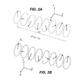
- FIG. 2 is an explanatory diagram illustrating a helical spin structure proposed in an embodiment of the present disclosure, in which the arrangement of the spins before the current flows (FIG. 2A), the spins generated as a result of the interaction with the conduction electrons. (FIG. 2B).
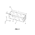
- FIG. 3 is a configuration diagram illustrating a configuration example of the inductor element according to the embodiment of the present disclosure. 4, in embodiments of the present disclosure is an explanatory diagram showing collectively elevation phi 0 in each range of the angular frequency omega.
- FIG. 1 is an explanatory diagram for explaining the operation principle of a conventional inductor element.
- FIG. 2 is an explanatory diagram illustrating a helical spin structure proposed in an embodiment of the present disclosure, in which the arrangement of the spins before the current flows (FIG. 2A), the spins generated as a result of the interaction with the conduction electrons. (FIG
- FIG. 5 is an explanatory diagram illustrating a non-collinear spin structure according to an embodiment of the present disclosure, and shows a cycloidal structure spin structure (FIG. 5B) as compared with a spiral structure (FIG. 5A).
- FIG. 6 is an SEM (scanning electron microscope) image of a sample of the inductor element in the embodiment of the present disclosure.
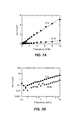
- FIG. 7 is a graph showing the measurement results of the frequency characteristic of the voltage drop of the sample of the inductor element according to the embodiment of the present disclosure, which is on a linear scale (FIG. 7A) and on a logarithmic scale (FIG. 7B).
- FIG. 1 is an explanatory diagram for explaining the operation principle of a conventional inductor element.
- a potential difference V proportional to a time change of the current I is generated by electromagnetic induction.
- the relationship is determined by using the inductance L Is expressed as
- the most typical inductor element is the coil shown in FIG.
- Electrons behave as small magnets due to their angular momentum h-bar / 2.
- h-bar is a value obtained by dividing the Planck constant h by 2 ⁇ .
- the spin of an electron is a component for a higher-order structure (magnetic structure or magnetic order) that expresses the magnetic properties of a substance such as ferromagnetism.
- What determines the magnetic order in a material is the arrangement of ordered electron spins (ordered spin), that is, the spin structure.
- the ordered spin that can take a spin structure is typically a localized electron spin (localized spin) or a conduction electron spin when the conduction electron itself forms magnetic order.
- the spin structure may have a parallel (parallel) spin structure or an anti-parallel spin structure.
- the parallel spin structure and the antiparallel spin structure are the origins of the ferromagnetic order and the antiferromagnetic order, respectively, and are both spatially uniform. Structures that are spatially uniform and parallel or antiparallel, such as a parallel spin structure and an antiparallel spin structure, are also called collinear spin structures. On the other hand, it is also known that a tilted spin structure in which near spins are neither parallel nor antiparallel is realized in a substance, and is called a non-collinear spin structure (non-collinear spin structure). I have.
- the operation of the inductor element of the present embodiment involves the non-collinear spin structure.
- the wave function of conduction electrons propagating there is influenced by the spatial structure of the ordered spin through Hund coupling, and a spinberry phase occurs.
- the spinberry phase acts similarly to the vector potential of the electromagnetic field.
- the action of the spinberry phase on the conduction electrons can be described by an electromagnetic field ("emergent electromagnetic fields"), which is a vector potential having an equivalent action.
- a vector n representing a spin structure created by the spin orientation of localized electrons in a substance is introduced.
- the vector n has one direction for each position in the xyz rectangular coordinate system, and has time dependency.
- the generating magnetic field that describes the effect that has on conduction electrons is Can be generally described as
- subscript i, j, k are orthogonal coordinates x, y, is selected cyclically indicates whether a component of any of the axes of z, e i, b i are respectively wound generator field, the emergent field
- the components, i i and t t are the partial derivative at spatial coordinate i and the partial derivative at time t, respectively.
- the motion of the conduction electrons is determined according to the superposition of the generated magnetic field generated in this way in addition to the external electromagnetic field.
- the wound power generating field vector e (e x, e y , e z) as the resistivity [rho, Create a current density J vector of The voltage drop V generated in the conduction electrons accordingly Towards, the current density vector J and the direction of the line through which the current flows coincide, the component of the direction of the generating power generation field vector e is e, and the length of the line is l.
- Non-Patent Document 4 it is known that a voltage drop in a helical structure is caused by deforming a helical spin structure by a magnetic field.
- the present inventor has noticed that when a current is applied to a substance having a non-collinear spin structure, emf is generated therein, and the spin structure itself is also deformed. Moreover, the inventors have realized that the voltage drop is not a simple resistance but can lead to an operation of an inductance. In particular, it has also been found that the inductor element that performs such an operation has a performance dependency on the element size which is advantageous for miniaturization.
- FIG. 2 is an explanatory diagram illustrating a spin structure of a spiral structure proposed in the present embodiment, and FIG. 2A shows an arrangement of ordered spins before a current flows.
- the position of the ordered spin is fixed at, for example, a lattice point (such as an atom) not shown.
- the ordered spin at each position points in the plane of a certain plane (xy plane), and if the direction is traced in a direction perpendicular to the plane (the direction of the z axis), the order is proportional to the distance. Rotate in the xy plane.
- ⁇ for a half rotation is the distance required for the spin to be reversed, and corresponds to the thickness of the domain wall separating two adjacent magnetic domains in the ferromagnetic order.
- Non-patent Document 2 Non-patent Document 2
- Non-patent Document 3 observation in which a potential difference occurs in the domain wall portion by applying a conventional magnetic field
- the domain wall parallel to the xy plane is used.
- 2B shows the deformation of the spin structure resulting from the interaction with conduction electrons, that is, the rise of ordered spins in the z-axis direction (perpendicular to the plane).
- the effect of accumulating energy as magnetic field energy appears as a voltage drop (Equation (1))
- the deformation of the rise of the localized spin of the helical structure occurs. Is responsible for energy storage. At that time, the conduction electrons that carry the current that caused the energy storage detect a voltage drop due to the generating field.
- FIG. 3 is a configuration diagram illustrating a configuration example of the inductor element of the present embodiment.
- the inductor element 10 includes a metal medium 2 having a non-collinear spin structure inside. If the spin structure is a helical structure, the outer shape of the metal medium 2 will most typically be oriented along the z-axis so that current is directed along the z-axis (FIG. 2A), which is the direction of the wave number Q of the helical structure. It extends along it. A current I flows through the metal medium 2 in the direction in which the current I extends.
- the current I generates a generating field, and the conduction electrons carrying the current I detect it.
- the direction of the current I is more generally any direction that can generate a generating field from the current by the non-collinear spin structure.
- the localized spins are spatially oriented so as to have a non-collinear spin structure when tracing in a certain direction (the z-axis direction in FIG. 3)
- the outer shape of the metal medium 2 flows therethrough.
- the current is formed to have a component projected in the direction of the z-axis giving a non-collinear spin structure.
- FIG. 3 illustrates, by way of example, the configuration of an inductor element 10 that employs a metal medium 2 having a non-collinear spin structure having a helical structure shown in FIG. 2, and changes the spin direction shown in FIG. Although the arrows are not shown, they represent the representation of the disk 4 containing spins.
- the metal medium 2 has a cross-sectional area A and a length 1 at least locally, and a current I flows across the length 1 across the cross-sectional area. Since the inductor element 10 is generally connected to an electric circuit, the current I is a current flowing through the inductor element 10 by the electric circuit.
- FIG. 3 illustrates the metal medium 2 as a rectangular parallelepiped, the metal medium 2 can take any shape or form as long as the above relationship with the non-collinear spin structure is satisfied. And may have any other pattern or outer shape.
- a vector n indicating the structure of the helical spin shown in FIG. 2A is determined only in z in the xyz rectangular coordinates, and the vectors e 1 , e 2 , and e 3 are defined as unit vectors in the xyz rectangular coordinates, respectively. Is described.
- the vector n indicating the direction of the localized spin is oriented in the xy plane when m is 0, and at each position having a length of 1 depending on the direction z and the magnitude Q of the helical wave vector, Is a vector.
- the vector tip draws a spiral.
- m is a component of rising in the z-axis direction, and if m is non-zero, it means having rising.
- the translational coordinate X of the helical structure is introduced with respect to the position of the z-axis, And X reflects ⁇ representing the phase of the helical structure maintaining the wave number Q, and can be said to indicate the centroid position of the helical structure.
- the equation of motion followed by spin is also known as the LLG (Landau-Lifshitz-Gilbert) equation. Taking into account the interaction of the current by conduction electrons, the equation of motion for the spin structure is as follows: ⁇ 0 is defined as the angle (elevation angle) at which the spin occurs from the xy plane in the plane perpendicular z direction.
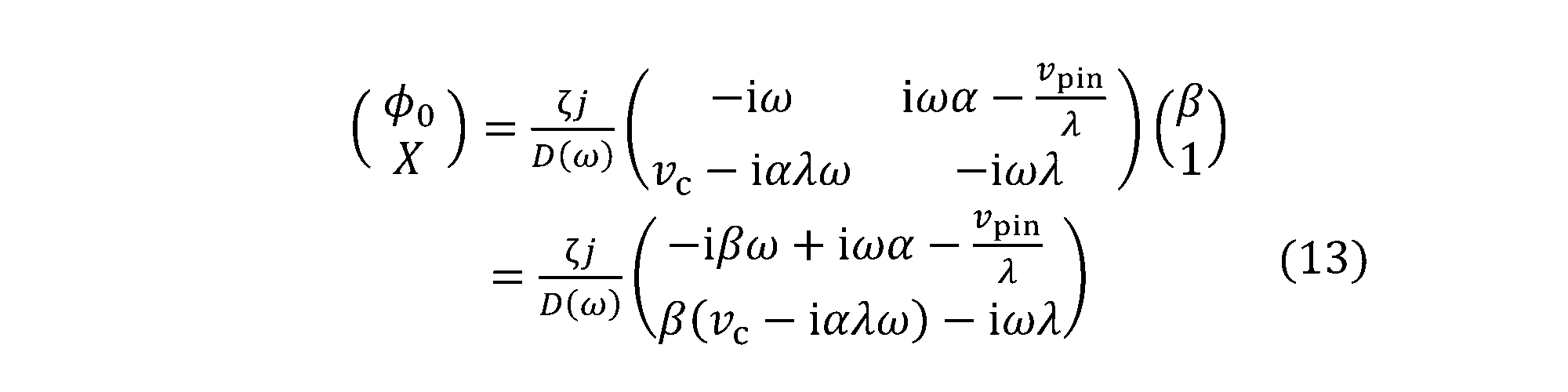
- Equation (11) is linearized using time dependency exp ( ⁇ i ⁇ t) (where i is an imaginary unit) assuming that the required physical quantity is represented by the real part of a complex number, And can be organized.
- Equation (15) is a general equation for deformation of the spin structure.
- two physical quantities based on physical considerations are introduced. These have the same physical dimension (dimension) as the current density j, and have a threshold aspect based on the pinning action, as follows.
- j int is a current density corresponding to a threshold value that overcomes spin anisotropy of the spin structure itself.
- j pin is a current density corresponding to a threshold value that overcomes pinning due to impurities.
- the spin of the anisotropy K ⁇ of intrinsic pinning is about 0.03K ⁇ 2.4K.
- the intrinsic pinning is a function of pinning the spin so as not to cause the spin to rise in the z-axis direction, and the anisotropy K ⁇ gives a strong restoring force. This is the amount that must be won for the spin to actually rise.
- L is proportional to A as shown in Expression (2), whereas in the inductor element of the present embodiment, Expressions (31) and (32) are used. ), L is inversely proportional to A. That is, the inductor element that operates according to the principle of the present embodiment has a property that is extremely favorable for element miniaturization, in which L can be increased by decreasing the cross-sectional area A.
- FIG. 5 shows a cycloidal spin structure in comparison with a helical structure (also known as a proper helix structure, FIG. 5A) (FIG. 5B).
- the spin number at each position is included in the xz plane, and the wave number of the periodic structure is oriented in the z-axis direction.
- the elevation angle phi 0 is generated in the helical axis direction.
- an elevation angle ⁇ 1 (not shown) from the xz plane to the y-axis direction is generated.
- ⁇ ⁇ The voltage drop does not depend on the spin rotation plane. This is because the inductance always appears in the same direction with respect to the current flowing in the direction of the spin modulation vector.
- a structure in which a spiral structure and a cycloidal structure are combined can be used as an inductor element. For example, in FIG. 3, if a multi-dimensional spin structure is considered, for example, a combination structure such as a spiral structure in the z-axis direction and a cycloidal structure in the y-axis direction can be adopted.
- a spin structure having a large wave number occurs in the spin when viewed in a certain direction of the zy plane, and when following the direction, the disk rotates on a disk inclined from the direction of the wave number vector. It becomes a spin structure.
- the inductor element of the present embodiment includes Can function as
- non-collinear spin structures can be adopted for the inductor element of the present embodiment.
- a cone (conical) spin structure that rises from a helical structure so as to have a certain angle of elevation in advance, or a slope in which the spin is directed along a conical surface that has a cone axis inclined from the wavenumber direction of the periodic structure
- the inductor element of the present embodiment can be similarly implemented using a material exhibiting a conical spin structure.
- the spiral structure, cycloidal structure, conical spin structure, inclined conical spin structure, and fan structure are all non-collinear spin structures, but there are also skyrmions and spin structures with three-dimensional frustration. It can be employed to implement the inductor element of the present embodiment.
- FIG. 6 is an SEM (scanning electron microscope) image of a sample of the inductor element 10 in the present embodiment.
- a metal medium 102 was obtained by forming a thin film of Gd 3 Ru 4 Al 12 having a thickness of 0.3 ⁇ m into a rectangle having a width of 10 ⁇ m and a length of 20 ⁇ m.
- rectangular Gd 3 Ru 4 Al 12 was formed on a silicon substrate by a microsampling method using a focused ion beam.
- electrodes 114 to 128 made of tungsten were formed on both short sides (entire width) and both long sides (positions where the distance between the electrodes was 7 ⁇ m on each side) of the metal medium 102.
- Gold thin film wirings 134, 136, 142, 144, 146, and 148 for connection to an external circuit are connected to each electrode.
- the gold thin film wirings 134, 136, 142, 144, 146, and 148 were formed by electron beam evaporation and patterned by UV lithography and lift-off.
- the electrodes 114 to 128 were formed so as to connect the thin metal wirings 134, 136, 142, 144, 146, and 148 to the metal medium 102 by a focused ion beam assisted vapor deposition method.
- the short sides are the drive electrodes 114 and 116 for passing a current through the inductor element sample 110, and the long sides are the probe electrodes 122, 124, 126 and 128 for measuring the voltage drop in the length direction.
- the measurement target is a voltage drop between the probe electrodes 122 and 124 or between the probe electrodes 126 and 128 when an alternating current is applied between the drive electrodes 114 and 116.
- the voltage drop measures a component having the same frequency as that of the applied AC current.
- FIG. 7 is a graph showing the measurement results of the frequency characteristics of the voltage drop of the inductor element sample 110, which are on a linear scale (FIG. 7A) and on a logarithmic scale (FIG. 7B).
- the vertical axis represents the voltage drop ( ⁇ phase component) appearing in the imaginary part (phase advance component) of the AC potential difference between the probe electrodes 122 and 124. ImV).
- the frequency ⁇ was measured from 0 to 10 KHz
- the alternating current applied between the drive electrodes 114 and 116 was set to a current density of 3.3 ⁇ 10 8 A / m 2 .
- the temperature environment was measured at each of 5K and 15K in order to secure operation stability and measurement accuracy.
- the voltage drop V is determined by the inductance L of the inductor element, the current I, and the angular frequency ⁇ .
- ImV ⁇ LI (34) Holds.
- the measurement result of FIG. 7 in which a voltage drop proportional to the frequency is observed in the frequency band of 0 to 10 kHz indicates that the inductor element sample 110 actually functions as an inductance element.
- the inductance (L) at that time is substantially constant.
- the size and mass of the inductor element sample 110 are extremely small.
- its mass is less than or equal to 1 ngram or 10 ⁇ 9 g.
- the size of only the metal medium 102 is about 0.65 ng.
- the inductor element provided in the present embodiment can have an equivalent inductance value with a size and mass of about 10 ⁇ 6 of the conventional inductor element.
- [Pt (3 nm) / Co (0.9 nm) / Ta (4 nm)] 15 is a composite material heterostructure of a platinum-based heterostructure having a unit structure of Pt / Co / Ta.
- Each metal layer in the unit structure has a thickness (nm unit) in parentheses, and is manufactured in a laminated structure in which 15 unit structures are repeatedly laminated. [Ir (10) / Fe (0-6) / Co (4-6) / Pt (10)] 20 and [Pt (3nm) / Co (0.9nm) / Ta (4nm)] 15 domain walls
- the lower limit of the width is about 80 nm (Non-Patent Document 6) and about 90 nm (Non-Patent Document 7). For this reason, it can be expected that the pitch of the spiral structure can be considerably shortened.
- a substance having a non-collinear spin structure can be adopted.
- the non-collinear spin structure is a spin structure of a localized spin that has been modulated from ferromagnetic order by a spin-orbit interaction represented by the Jaroshinsky-Moriya interaction, and is selected from those described above, for example, a helical structure. .
- Such materials can typically be selected from alloys containing transition metals.
- a substance that realizes a non-collinear spin structure between localized spins as a result of RKKY interaction, which is another generation mechanism different from spin-orbit interaction, can also be used.
- the non-collinear spin structure is realized between localized spins by magnetic frustration, and a material suitable for the inductor element of the present embodiment can be selected from such a substance group.
- Device The present disclosure also includes a device on which an electric / electronic circuit including the above-described inductor element is mounted.
- the integrator element of the embodiment described above can be employed as a basic element for a general electric / electronic circuit including, for example, a resonance circuit and a filter circuit.
- the above-mentioned inductor elements can be applied in principle without limitation, they include general electric / electronic devices including these electronic circuits, regardless of industrial or home use, electric / electronic devices, communication devices, Includes audiovisual equipment and medical electronic equipment. Since the inductor element provided in the present disclosure can be made lightweight and compact, it can also be applied to hearing aids, cardiac pacemakers, and microelectromechanical systems (MEMS).
- MEMS microelectromechanical systems
- the present disclosure can be used for any device including an inductor element in a circuit.
Landscapes
- Engineering & Computer Science (AREA)
- Power Engineering (AREA)
- Microelectronics & Electronic Packaging (AREA)
- Chemical & Material Sciences (AREA)
- Crystallography & Structural Chemistry (AREA)
- Materials Engineering (AREA)
- Coils Or Transformers For Communication (AREA)
- Hall/Mr Elements (AREA)
- Hard Magnetic Materials (AREA)
- Thin Magnetic Films (AREA)
Abstract
Description
1-1.従来のインダクター素子での微細化の困難性
図1は、従来のインダクター素子の動作原理を説明するための説明図である。インダクター素子では、電磁誘導によって電流Iの時間変化に比例した電位差Vを生じさせる。その関係はインダクタンスLを用いて


本実施形態においては、利用する動作原理が従来のものとは全く異なり、電子のスピンと伝導電子との相互作用を利用する。




図2は、本実施形態にて提案されるらせん構造のスピン構造を例示する説明図であり、図2Aは電流を流す前の秩序スピンの配置を示している。秩序スピンは、例えば図示しない格子点(原子など)に位置が固定されている。ある時刻において、各位置の秩序スピンはある平面(xy平面)の面内を向いており、その向きを、当該平面に垂直な向き(z軸の向き)にたどると、その距離に比例してxy平面内で回転する。このらせん軸の向きに位置的な周期2λでスピンの向きが一周するとき、らせん構造の波数QがQ=2π/(2λ)と決定できる。なお、半回転分のλは、スピンが反転するのに要する距離であり、強磁性秩序において隣り合う2つの磁区を仕切る磁壁の厚みに対応している。z軸をそのらせん構造のもつ周期構造の波数Qの軸に定めても一般性は失われないので、本開示での説明はそのような向きに直交座標を仮定している。なお、従来の磁場を印加して磁壁部分に電位差が生じる理論的予測(非特許文献2)や、観測(非特許文献3)では、図2Aに示したらせん構造において、xy平面に平行な磁壁がz軸に垂直な向き(例えばx軸)に向いた外部磁場の作用によりz方向に動くことが確かめられている。これらは、磁場のみによって磁区を制御することのみを開示している。
本発明者は、らせん軸の向きであるz軸方向に時間的に変動する交流電流を流す配置において、創発電場e(式(4))により電圧降下(式(6))が効率良く生じることを見出した。そのような電流を流すと、電流を担う伝導電子はスピン構造と相互作用する。その1つは図2Aのz軸回りにスピン構造全体を回すような回転作用である。さらに、回転するスピン構造には、伝導電子との相互作用によりそれ自体にも変形が生じる。図2Bは、伝導電子との相互作用の結果生じるスピン構造の変形、つまり秩序スピンのz軸方向(面直方向)への起き上がりを示している。従前のインダクター素子では磁場エネルギーとしてエネルギーを蓄積する作用が電圧降下(式(1))となって現われていたのに対し、本実施形態のインダクター素子では、らせん構造の局在スピンの起き上がりの変形がエネルギーの蓄積を担う。その際に、そのエネルギー蓄積の原因となった電流を担っている伝導電子は、創発電場による電圧降下を検知するのである。
ここで、本実施形態のインダクター素子の構成を説明する。図3は、本実施形態のインダクター素子の構成例を示す構成図である。インダクター素子10は、内部に非共線スピン構造を備える金属媒体2を備えている。スピン構造がらせん構造であれば、最も典型的には、そのらせん構造の波数Qの方向であるz軸(図2A)にそって電流が導かれるように、金属媒体2の外形はz軸にそって延びるようになっている。金属媒体2には電流Iがその延びる向きに向かって流される。これにより、らせん構造(より一般には非共線スピン構造)の秩序スピンに対し、電流Iが創発電場を生じさせ、電流Iを担う伝導電子がそれを検知することとなる。電流Iの方向は、より一般には、非共線スピン構造によって電流から創発電場を生成できる任意の向きである。例えば、ある方向(図3においてz軸方向)にたどったときに局在スピンが非共線スピン構造をもつように空間的に配向しているものでは、金属媒体2の外形は、そこを流れる電流が非共線スピン構造を与えるz軸の方向に射影した成分をもつように形成される。図3には、例示として、図2に示したらせん構造の非共線スピン構造をもつような金属媒体2を採用したインダクター素子10の構成を描いており、図2に示したスピンの向きを示す矢印は示していないが、スピンが含まれている円盤4の表現を描いている。金属媒体2は少なくとも局所的には断面積Aと長さlをもっておりこの断面積を横切るように長さlにわたって電流Iが流される。インダクター素子10は一般には電気回路に接続されるため、電流Iはその電気回路がインダクター素子10に流す電流である。なお、図3では金属媒体2は直方体に描いているが、非共線スピン構造との上記関係が満たされる限り任意の形状や形態を取ることができ、例えば薄膜、フィルム、配線とすることができ、他の任意のパターンや外形形状をもちうる。








jint:intrinsic pinningによる閾値電流密度
ζjint=vc/2
jpin:extrinsic pinningによる閾値電流密度
ζβjpin=vpin
ここでjintは、スピン構造自体がもつスピンの異方性に打ち勝つ閾値に対応する電流密度である。これに対しjpinは、不純物によるピンニングに打ち勝つ閾値に対応する電流密度である。さらに特徴的な2つの周波数
νint=vc/λ
νpin=vpin/λ
でこれらを置き換えると、式(15)は

A-(i) ω≪νpin/α≪νint
この場合、
分母≒-νpinνint
となるので、

A-(ii) νpin/α≪ω≪νint
この場合、
分母≒iαωνint、分子≒iω(β-α)
となるので、

A-(iii) νint≪ω
この場合、
分母≒ω2、分子≒iω(β-α)
となるので、

B-(i) ω≪ανint≪νpin≪νint
この場合、
分母≒iαωνint-νpinνint≒-νpinνint
(∵iαωνint≪iα2νint)
分子≒νpin
となるので、

B-(ii) ανint≪ω≪(νpinνint)1/2
この場合、
分母≒-νpinνint
分子:αω/νpin≪α(νint/νpin)1/2≪α(1/α)1/2=α1/2
∴分子≒νpin
となるので、

B-(iii) (νpinνint)1/2≪ω≪νint
この場合、
分母≒ω2
分子:αω/νpin≫(νint/νpin)1/2≫1
∴分子≒iω(β-α)
となるので、

創発電場をらせんのスピン構造に対応して整理するには、式(6)に示したスピン磁場構造に対して式(4)を求めればよい。

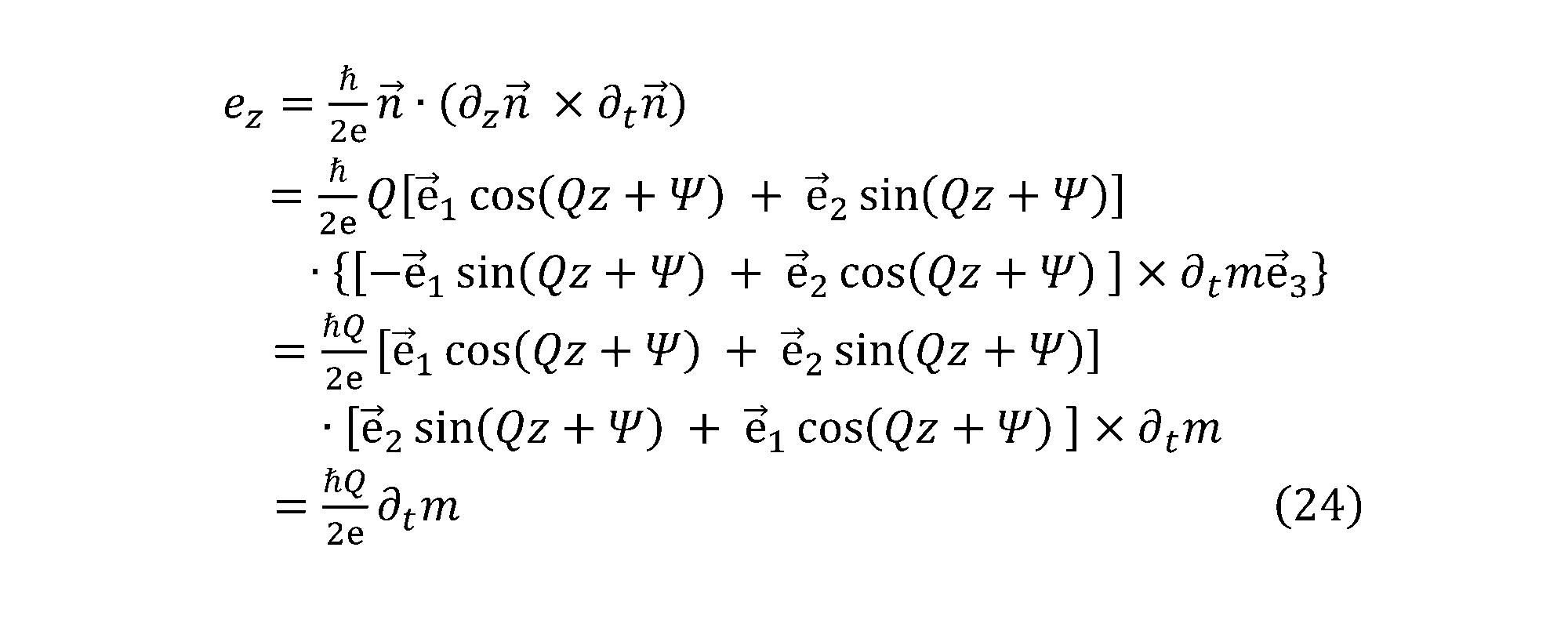

定式化した各関係式に、実際の物質についての物理量の値や現実的値、定数値などを適用して関連する各物理量を見積り、インダクター素子の性能を予測した。
まず、intrinsic pinningのスピンの異方性K⊥が0.03K~2.4K程度である。このintrinsic pinningは、スピンをz軸方向に向かって起き上がらせないようにスピンをピン止めしている作用であり、異方性K⊥は復元力の強さを与える。スピンが実際に起き上がるためにはこれに勝つ必要がある量といえる。vc∽K⊥の関係に基づき、閾値電流密度jintすなわちピン止めに打ち勝つために必要な最小限の電流閾値を求めると、jint=5×10¹¹~4×10¹³A/m2と見積もることができる。ただしこの値は、DC(直流)の電流で起き上がらせるために最小限必要となる電流密度であるため、AC(交流)電流を印加する場合には、電流値に比例した量だけスピンの起き上がりが生じる。

λ=20nm=2×10⁻⁸m
e=1.6×10⁻¹⁹C
h-bar=10-31J・sec
の各値を用いると、

V=lez=1.5×10⁻⁷×ν×10-3(Volt)
=1.5×10⁻¹⁰×ν(Volt)
となる。検出電圧下限をnVolt(10-9V)とすると、周波数ν(=ω/2π)の下限は数Hz程度から検出が可能となり、創発電場の発現は実験的に確認可能である。
次にνint、νpinの値を見積もる。一方のνintについては、一般的な金属の伝導特性をもつ物質を想定すると、局在スピンの大きさS~1、電子密度n、格子定数aとして、na3~1、閾値電流密度jint~1012A/m2となって、
vc/2=ζjint=a3Pjint/2eS
となる。P=0.1、a=4nmを用いると、
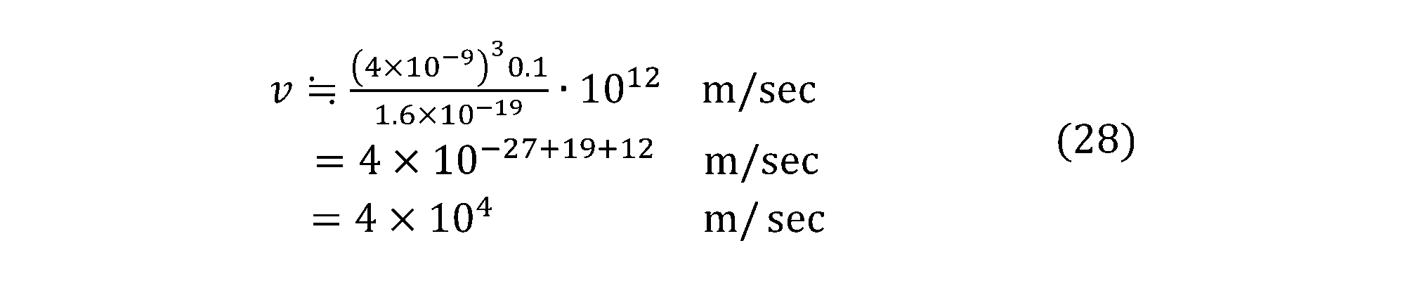
νint=vC/λ=(4×104)/(2×10-8)=2×1012sec-1
と見積もることができる。
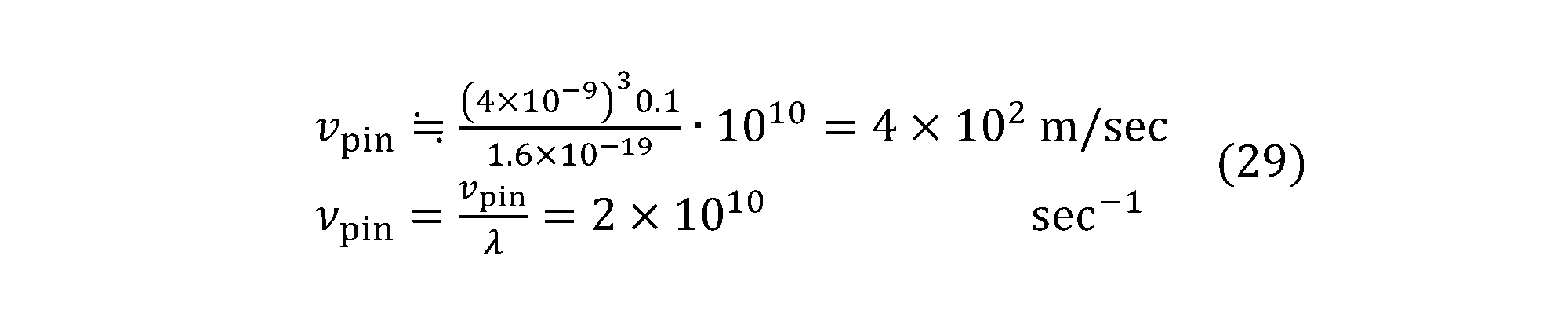
つぎにインダクター素子としての特性を説明する。断面積A、長さlの線状導体、その延びる向きをらせん構造の波数方向にあわせて作製した場合(図3)のインダクタンスLを見積もる。式(1)において、V=lez、電流値I=jAとし、


L≒1/2×10-10[Henry]
と算出される。
本実施形態のインダクター素子の性能予測のために、さらにインダクター素子の性能指標であるQ値を算出する。
Q=Lω/R=2πLν/R
であり、
R=ρl/A
であるため、これらに式(32)を代入すれば、

図4に戻り、仰角φ0についての知見のいくつかを説明する。仰角φ0が角周波数ωに対してどのように振る舞うかは図4に示した通りである。時間項の角周波数ωが小さくDCに近い動作では、ケースA、Bのいずれにおいても、電流密度jのintrinsic pinningの閾値電流密度jintに対する割合が仰角φ0のスケールを決定している。これが、DCで閾値電流密度jintが重要となる理由である。ただし、高周波ではむしろ閾値電流密度jintは無関係である。また、仰角φ0がβ-αに比例しているケースがある(A-(ii)A-(iii)B-(iii))。これは、減衰項であるαと非断熱効果項βが等しくなるという特殊な条件が満たされた場合、仰角φ0が生じないことを意味する。その仰角φ0が生じない場合には、スピン構造に含まれる各秩序スピンは伝導電子の電流に応じて起き上がろうとはしない。この場合のらせん構造のスピン構造は、z軸方向に平行移動するのみである。なお、仰角にかかわらず、らせん構造のz軸周りの単純な回転は、z軸周りにらせん構造自体が平行移動したものと区別できず、同視される。また、仰角φ0が生じない場合にはインダクタンスも生じない。しかし、実際のスピン構造ではβ≠αと考えて良いため、仰角φ0が生じるともに、インダクタンスが生じることが十分に期待できる。
本実施形態のインダクター素子は、らせん構造以外の非共線スピン構造を採用しても同様に機能しうる。そのようなスピン構造の1つが、サイクロイダル構造である。図5に、らせん構造(別名、プロパーヘリックス構造、図5A)と対比してサイクロイダル構造のスピン構造を示している(図5B)。
発明者は、この発明分野に関し国立研究開発法人日本科学技術振興機構戦略的創造研究推進事業(CREST)課題として、基礎出願後の2018年に採択された後に、本実施形態で提案されるインダクター素子の動作実証を行った。図6は、本実施形態においてインダクター素子10のサンプルのSEM(走査型電子顕微鏡)像である。インダクター素子サンプル110ではGd3Ru4Al12の厚み0.3μmの薄膜を幅10μm、長さ20μmの矩形に形成したものを金属媒体102とした。具体的には、シリコン基板に収束イオンビームによるマイクロサンプリング法により矩形のGd3Ru4Al12を形成した。さらに、金属媒体102の両短辺(全幅)と両長辺(各辺において電極間距離7μmとなる位置)にはタングステンによる電極114~128を形成した。各電極には、外部回路との接続のための金薄膜配線134、136、142、144、146、148を接続している。具体的には、金薄膜配線134、136、142、144、146、148は、電子ビーム蒸着法により成膜し、UVリソグラフィーとリフトオフ法によりパターニングした。また、電極114~128は、収束イオンビームアシスト蒸着法により、金薄膜配線134、136、142、144、146、148と金属媒体102とをつなぐように形成した。短辺のものはインダクター素子サンプル110に電流を流す駆動電極114、116、長辺のものは、長さ方向での電圧降下を計測するためのプローブ電極122、124、126、128である。
ImV=ωLI (34)
の関係が成り立つ。これを考慮すれば、0~10kHzの周波数帯で周波数に比例した電圧降下が観測された図7の測定結果が示しているのは、インダクター素子サンプル110が実際にインダクタンス素子として機能していること、およびその際のインダクタンス(L)が略一定であることである。
0.3μm×10μm×7μm=21×10-9mm3
であり、その質量は1nグラムつまり10-9g以下である。具体的に密度と体積から質量を計算すると、Gd3Ru4Al12の密度(10.8g/cm3)とサンプルにおける体積(およそ10×20×0.3μm3)から、電極や基板を含めない金属媒体102だけのサイズをみると0.65ng程度になる。
(0.6mm×0.3mm×0.3mm)=54×10-3mm3
程度である。このように、本実施形態にて提供されるインダクター素子は、従来のインダクター素子の10-6程度のサイズおよび質量で同等なインタクタンス値をもちうる。
次に、非共線スピン構造を実現し、本実施形態のインダクター素子として動作させうる材料について説明する。上述した説明から、隣接するスピンどうしがほぼ強磁性秩序(概ね平行に向く秩序)をもち、そこからの変調の結果として非共線スピン構造を実現しており、実用的な電気伝導度を示す金属材料、が典型的な選択基準である。このような性質を満たす非限定的な材料の例を表1に示す。
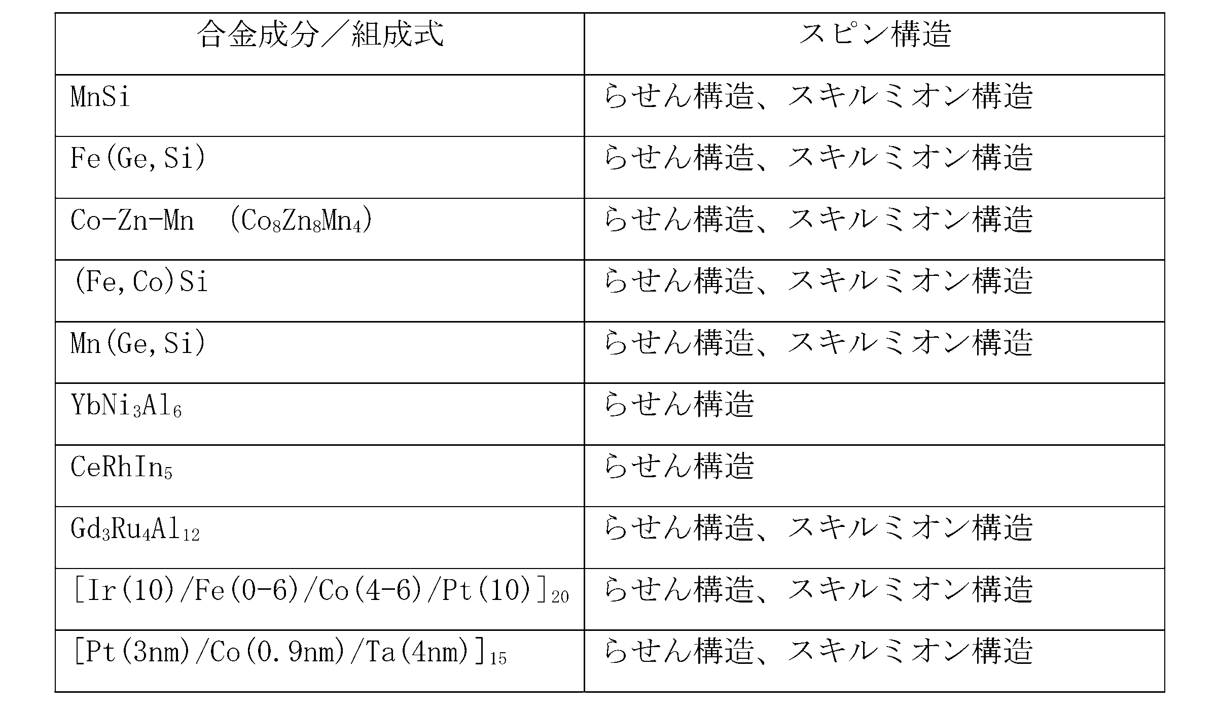
これらの一例として、MnSiは、カイラル磁性体であり、らせん構造を取ることができる。なお、MnSiは特定の条件ではスキルミオン構造も取りうる。[Ir(10)/Fe(0-6)/Co(4-6)/Pt(10)]20は、Ir/Co/PtまたはIr/Fe/Co/Ptの単位構造をそなえるプラチナ系のヘテロ構造体の複合素材であり、単位構造内では各金属層が括弧内の厚み(単位:オングストローム=0.1nm)をもつ。この例では、20単位構造を繰り返し積層した積層構造をもつ。また、[Pt(3nm)/Co(0.9nm)/Ta(4nm)]15は、Pt/Co/Taの単位構造を備えるプラチナ系のヘテロ構造体の複合素材ヘテロ構造体である。単位構造内で各金属層が括弧内の厚み(nm単位)をもち、15単位構造を繰り返し積層した積層構造に作製される。[Ir(10)/Fe(0-6)/Co(4-6)/Pt(10)]20、および[Pt(3nm)/Co(0.9nm)/Ta(4nm)]15のドメイン壁幅の下限値はそれぞれ80nm程度(非特許文献6)、および90nm程度(非特許文献7)である。このため、らせん構造のピッチを相当程度短くできることが期待できる。
本開示は、上述したインダクター素子を含む電気・電子回路を搭載する機器も含んでいる。上述した実施形態のインタクター素子は、例えば共振回路、フィルター回路を含む一般的な電気・電子回路のための基本素子として採用することができる。上述したインダクター素子が原理的に適用可能なものは特段限定されないが、これらの電子回路を含む一般の電気・電子機器を含み、産業用または家庭用を問わず、電気・電子機器、通信機器、オーディオ・ビジュアル機器、医療関係の電子機器を含んでいる。本開示で提供されるインダクター素子は軽量かつコンパクトに作製しうるため、補聴器、心臓ペースメーカー、およびMEMS(microelectromechanical systems)への適用も可能である。
2 金属媒体
4 円盤(非共線スピン構造を示す)
110 インダクター素子サンプル
102 金属媒体
114、116、122、124、126、128 電極
134、136、142、144、146、148 金薄膜配線
Claims (5)
- ある方向にたどったときに非共線スピン構造をもつように秩序スピンが空間的に配向している金属媒体を備え、電流が該方向の射影成分をもつように該金属媒体を流されるインダクター素子。
- 前記金属媒体は、前記方向を波数方向としてもつらせん構造の前記空間的配向をもつ材質である
請求項1に記載のインダクター素子。 - 前記金属媒体は、前記方向を波数方向としてもつサイクロイダル構造の前記空間的配向をもつ材質である
請求項1に記載のインダクター素子。 - 前記金属媒体は、前記秩序スピンの隣接するもの同士がほぼ強磁性秩序をもっているものである
請求項1に記載のインダクター素子。 - 請求項1に記載のインダクター素子を含む機器。
Priority Applications (4)
| Application Number | Priority Date | Filing Date | Title |
|---|---|---|---|
| CN201980050902.7A CN112514012B (zh) | 2018-08-01 | 2019-08-01 | 电感元件以及包括该电感元件的器件 |
| US17/264,510 US12362085B2 (en) | 2018-08-01 | 2019-08-01 | Inductor element and apparatus including same |
| EP19844237.8A EP3832676B1 (en) | 2018-08-01 | 2019-08-01 | Inductor element and apparatus including same |
| JP2020534743A JP7385283B2 (ja) | 2018-08-01 | 2019-08-01 | インダクター素子およびそれを含む機器 |
Applications Claiming Priority (2)
| Application Number | Priority Date | Filing Date | Title |
|---|---|---|---|
| JP2018145483 | 2018-08-01 | ||
| JP2018-145483 | 2018-08-01 |
Publications (1)
| Publication Number | Publication Date |
|---|---|
| WO2020027268A1 true WO2020027268A1 (ja) | 2020-02-06 |
Family
ID=69231157
Family Applications (1)
| Application Number | Title | Priority Date | Filing Date |
|---|---|---|---|
| PCT/JP2019/030236 Ceased WO2020027268A1 (ja) | 2018-08-01 | 2019-08-01 | インダクター素子およびそれを含む機器 |
Country Status (5)
| Country | Link |
|---|---|
| US (1) | US12362085B2 (ja) |
| EP (1) | EP3832676B1 (ja) |
| JP (1) | JP7385283B2 (ja) |
| CN (1) | CN112514012B (ja) |
| WO (1) | WO2020027268A1 (ja) |
Cited By (5)
| Publication number | Priority date | Publication date | Assignee | Title |
|---|---|---|---|---|
| JP2022118907A (ja) * | 2021-02-03 | 2022-08-16 | 国立研究開発法人理化学研究所 | インダクター素子およびそれを含む機器 |
| WO2023238334A1 (ja) * | 2022-06-09 | 2023-12-14 | Tdk株式会社 | スピンインダクタ |
| WO2025009050A1 (ja) * | 2023-07-04 | 2025-01-09 | Tdk株式会社 | スピンインダクタ |
| WO2026033583A1 (ja) * | 2024-08-05 | 2026-02-12 | Tdk株式会社 | スピンインダクタ |
| WO2026033584A1 (ja) * | 2024-08-05 | 2026-02-12 | Tdk株式会社 | スピンインダクタ |
Families Citing this family (1)
| Publication number | Priority date | Publication date | Assignee | Title |
|---|---|---|---|---|
| CN118841235B (zh) * | 2024-07-11 | 2025-05-06 | 南京大学 | 无线圈式质子型电感器、设计方法及调控方法 |
Citations (1)
| Publication number | Priority date | Publication date | Assignee | Title |
|---|---|---|---|---|
| WO2015118748A1 (ja) * | 2014-02-10 | 2015-08-13 | 国立研究開発法人理化学研究所 | スキルミオンの駆動方法および駆動装置 |
Family Cites Families (12)
| Publication number | Priority date | Publication date | Assignee | Title |
|---|---|---|---|---|
| JP4690675B2 (ja) * | 2004-07-30 | 2011-06-01 | 株式会社東芝 | 磁気抵抗効果素子、磁気ヘッド、および磁気記録再生装置 |
| CN101903792A (zh) * | 2007-12-21 | 2010-12-01 | 皇家飞利浦电子股份有限公司 | 具有层合铁磁核和用于抑制涡流磁场的超导膜的电磁体 |
| DE102009021400A1 (de) | 2009-05-14 | 2010-11-18 | Forschungszentrum Jülich GmbH | Magnetoelektronische Bauelemente und Messverfahren |
| JP6450389B2 (ja) | 2014-08-07 | 2019-01-09 | 国立研究開発法人理化学研究所 | 磁気記憶媒体およびデータ記録装置 |
| JP6312925B2 (ja) | 2015-03-31 | 2018-04-18 | 国立研究開発法人科学技術振興機構 | スキルミオン生成装置、スキルミオン生成方法、および磁気記憶装置 |
| US9773540B2 (en) * | 2015-07-17 | 2017-09-26 | The Johns Hopkins University | Skyrmion based universal memory operated by electric current |
| CL2015003361A1 (es) | 2015-11-16 | 2017-08-04 | Univ Santiago Chile | Nanogenerador de campo magnético alterno que utiliza un nanohilo que permite ser aplicado en la generación corriente alterna a nivel de nanoescala; y método asociado |
| US9899071B2 (en) * | 2016-01-20 | 2018-02-20 | The Johns Hopkins University | Heavy metal multilayers for switching of magnetic unit via electrical current without magnetic field, method and applications |
| US20170260634A1 (en) * | 2016-01-29 | 2017-09-14 | John Timothy Sullivan | Enhanced Exothermic Reaction (EER) Reactor |
| WO2017222588A1 (en) * | 2016-06-21 | 2017-12-28 | Intel Corporation | In-plane current driven magnetic skyrmion spin oscillator |
| WO2019155957A1 (ja) * | 2018-02-06 | 2019-08-15 | 国立大学法人東北大学 | 磁気抵抗効果素子、回路装置及び回路ユニット |
| GB201806425D0 (en) * | 2018-04-20 | 2018-06-06 | Provost Fellows Found Scholars And The Other Members Of Board Of The College Of The Holy And Undivid | Single magnetic-layer microwave oscillator |
-
2019
- 2019-08-01 US US17/264,510 patent/US12362085B2/en active Active
- 2019-08-01 CN CN201980050902.7A patent/CN112514012B/zh active Active
- 2019-08-01 JP JP2020534743A patent/JP7385283B2/ja active Active
- 2019-08-01 EP EP19844237.8A patent/EP3832676B1/en active Active
- 2019-08-01 WO PCT/JP2019/030236 patent/WO2020027268A1/ja not_active Ceased
Patent Citations (1)
| Publication number | Priority date | Publication date | Assignee | Title |
|---|---|---|---|---|
| WO2015118748A1 (ja) * | 2014-02-10 | 2015-08-13 | 国立研究開発法人理化学研究所 | スキルミオンの駆動方法および駆動装置 |
Non-Patent Citations (8)
| Title |
|---|
| "LQP03TN_02 series", MURATA MANUFACTURING CO., 18 July 2019 (2019-07-18), Retrieved from the Internet <URL:https://www.murata.com/en-global/products/emiconfun/inductor/2014/02/27/en-20140227-p1> |
| ANJAN SOUMYANARAYANAN ET AL.: "Tunable room-temperature magnetic skyrmions in Ir/Fe/Co/Pt multilayers", NATURE MATERIALS, vol. 16, 2017, pages 898 - 904 |
| GEN TATARAHIROSHI KOHNO: "Theory of Current-Driven Domain Wall Motion: Spin Transfer versus Momentum Transfer", PHYS. REV. LETT., vol. 92, 2004, pages 086601 |
| JUN-ICHIRO KISHINE ET AL.: "Coherent sliding dynamics and spin motive force driven by crossed magnetic fields in a chiral helimagnet", PHYS. REV. B, vol. 86, 2012, pages 214426 |
| PHAM NAM HAI ET AL.: "Electromotive force and huge magnetoresistance in magnetic tunnel junctions", NATURE, vol. 458, 2009, pages 489 - 492 |
| S. E. BARNESS. MAEKAWA: "Generalization of Faraday's Law to Include Nonconservative Spin Forces", PHYS. REV. LETT., vol. 98, 2007, pages 246601 |
| See also references of EP3832676A4 |
| SEONGHOON WOO ET AL.: "Observation of room-temperature magnetic skyrmions and their current-driven dynamics in ultrathin metallic ferromagnets", NATURE MATERIALS, vol. 15, 2016, pages 501 - 506, XP055750344, DOI: 10.1038/nmat4593 |
Cited By (6)
| Publication number | Priority date | Publication date | Assignee | Title |
|---|---|---|---|---|
| JP2022118907A (ja) * | 2021-02-03 | 2022-08-16 | 国立研究開発法人理化学研究所 | インダクター素子およびそれを含む機器 |
| JP7560871B2 (ja) | 2021-02-03 | 2024-10-03 | 国立研究開発法人理化学研究所 | インダクター素子およびそれを含む機器 |
| WO2023238334A1 (ja) * | 2022-06-09 | 2023-12-14 | Tdk株式会社 | スピンインダクタ |
| WO2025009050A1 (ja) * | 2023-07-04 | 2025-01-09 | Tdk株式会社 | スピンインダクタ |
| WO2026033583A1 (ja) * | 2024-08-05 | 2026-02-12 | Tdk株式会社 | スピンインダクタ |
| WO2026033584A1 (ja) * | 2024-08-05 | 2026-02-12 | Tdk株式会社 | スピンインダクタ |
Also Published As
| Publication number | Publication date |
|---|---|
| JPWO2020027268A1 (ja) | 2021-09-09 |
| CN112514012A (zh) | 2021-03-16 |
| EP3832676B1 (en) | 2025-04-23 |
| US12362085B2 (en) | 2025-07-15 |
| US20210383955A1 (en) | 2021-12-09 |
| EP3832676A4 (en) | 2022-05-04 |
| CN112514012B (zh) | 2024-03-08 |
| JP7385283B2 (ja) | 2023-11-22 |
| EP3832676A1 (en) | 2021-06-09 |
Similar Documents
| Publication | Publication Date | Title |
|---|---|---|
| JP7385283B2 (ja) | インダクター素子およびそれを含む機器 | |
| Soumyanarayanan et al. | Tunable room-temperature magnetic skyrmions in Ir/Fe/Co/Pt multilayers | |
| Uchida et al. | Observation of anisotropic magneto-Peltier effect in nickel | |
| Kanazawa et al. | Noncentrosymmetric magnets hosting magnetic skyrmions | |
| Hervé et al. | Stabilizing spin spirals and isolated skyrmions at low magnetic field exploiting vanishing magnetic anisotropy | |
| Gomonay et al. | Spintronics of antiferromagnetic systems | |
| Seki et al. | Skyrmions in magnetic materials | |
| Niimi et al. | Reciprocal spin Hall effects in conductors with strong spin–orbit coupling: a review | |
| US9088243B2 (en) | Magnetic field feedback based spintronic oscillator | |
| JP6611167B2 (ja) | 熱電変換デバイス及び熱電変換素子 | |
| JP7055480B2 (ja) | 低電力テラヘルツ磁気ナノ発振素子 | |
| Huang et al. | Layer-dependent magnetism and spin fluctuations in atomically thin van der Waals magnet CrPS4 | |
| Zhang et al. | Room-temperature highly-tunable coercivity and highly-efficient multi-states magnetization switching by small current in single 2D ferromagnet Fe3GaTe2 | |
| Birch et al. | Dynamic transition and Galilean relativity of current-driven skyrmions | |
| Lopez-Polin et al. | High-power-density energy-harvesting devices based on the anomalous Nernst effect of Co/Pt magnetic multilayers | |
| Kammerbauer et al. | Controlling the interlayer Dzyaloshinskii–Moriya interaction by electrical currents | |
| Han et al. | Spin pumping and probe in permalloy dots-topological insulator bilayers | |
| Yokouchi et al. | Emergent electric field induced by current-driven domain wall motion in a room-temperature antiferromagnet FeSn2 | |
| Zhou et al. | Orbital torque in Mn/FM bilayer systems | |
| WO2020090719A1 (ja) | スピントルク発生素子、その製造方法、及び、磁化制御装置 | |
| JP7560871B2 (ja) | インダクター素子およびそれを含む機器 | |
| Büttner et al. | Magnetic skyrmion dynamics | |
| JP2017112365A (ja) | スピントロニクスデバイス及びこれを用いた記憶装置 | |
| Kurebayashi et al. | Observation of a Berry phase anti-damping spin-orbit torque | |
| Xu et al. | Anisotropic anomalous Nernst effect of metallic nickel assembled by aligned nanowires |
Legal Events
| Date | Code | Title | Description |
|---|---|---|---|
| 121 | Ep: the epo has been informed by wipo that ep was designated in this application |
Ref document number: 19844237 Country of ref document: EP Kind code of ref document: A1 |
|
| ENP | Entry into the national phase |
Ref document number: 2020534743 Country of ref document: JP Kind code of ref document: A |
|
| NENP | Non-entry into the national phase |
Ref country code: DE |
|
| ENP | Entry into the national phase |
Ref document number: 2019844237 Country of ref document: EP Effective date: 20210301 |
|
| WWG | Wipo information: grant in national office |
Ref document number: 2019844237 Country of ref document: EP |
|
| WWG | Wipo information: grant in national office |
Ref document number: 17264510 Country of ref document: US |