WO2020031257A1 - 分布整合回路、分布整合終端回路、分布整合方法、分布整合終端方法および光伝送システム - Google Patents
分布整合回路、分布整合終端回路、分布整合方法、分布整合終端方法および光伝送システム Download PDFInfo
- Publication number
- WO2020031257A1 WO2020031257A1 PCT/JP2018/029578 JP2018029578W WO2020031257A1 WO 2020031257 A1 WO2020031257 A1 WO 2020031257A1 JP 2018029578 W JP2018029578 W JP 2018029578W WO 2020031257 A1 WO2020031257 A1 WO 2020031257A1
- Authority
- WO
- WIPO (PCT)
- Prior art keywords
- circuit
- information
- signal
- look
- signal point
- Prior art date
- Legal status (The legal status is an assumption and is not a legal conclusion. Google has not performed a legal analysis and makes no representation as to the accuracy of the status listed.)
- Ceased
Links
Images


Classifications
-
- H—ELECTRICITY
- H04—ELECTRIC COMMUNICATION TECHNIQUE
- H04L—TRANSMISSION OF DIGITAL INFORMATION, e.g. TELEGRAPHIC COMMUNICATION
- H04L27/00—Modulated-carrier systems
- H04L27/32—Carrier systems characterised by combinations of two or more of the types covered by groups H04L27/02, H04L27/10, H04L27/18 or H04L27/26
- H04L27/34—Amplitude- and phase-modulated carrier systems, e.g. quadrature-amplitude modulated carrier systems
- H04L27/3405—Modifications of the signal space to increase the efficiency of transmission, e.g. reduction of the bit error rate, bandwidth, or average power
- H04L27/3411—Modifications of the signal space to increase the efficiency of transmission, e.g. reduction of the bit error rate, bandwidth, or average power reducing the peak to average power ratio or the mean power of the constellation; Arrangements for increasing the shape gain of a signal set
-
- H—ELECTRICITY
- H04—ELECTRIC COMMUNICATION TECHNIQUE
- H04L—TRANSMISSION OF DIGITAL INFORMATION, e.g. TELEGRAPHIC COMMUNICATION
- H04L1/00—Arrangements for detecting or preventing errors in the information received
- H04L1/0078—Avoidance of errors by organising the transmitted data in a format specifically designed to deal with errors, e.g. location
- H04L1/009—Avoidance of errors by organising the transmitted data in a format specifically designed to deal with errors, e.g. location arrangements specific to transmitters
-
- H—ELECTRICITY
- H04—ELECTRIC COMMUNICATION TECHNIQUE
- H04B—TRANSMISSION
- H04B10/00—Transmission systems employing electromagnetic waves other than radio-waves, e.g. infrared, visible or ultraviolet light, or employing corpuscular radiation, e.g. quantum communication
- H04B10/50—Transmitters
- H04B10/516—Details of coding or modulation
- H04B10/5161—Combination of different modulation schemes
-
- H—ELECTRICITY
- H04—ELECTRIC COMMUNICATION TECHNIQUE
- H04L—TRANSMISSION OF DIGITAL INFORMATION, e.g. TELEGRAPHIC COMMUNICATION
- H04L27/00—Modulated-carrier systems
- H04L27/32—Carrier systems characterised by combinations of two or more of the types covered by groups H04L27/02, H04L27/10, H04L27/18 or H04L27/26
- H04L27/34—Amplitude- and phase-modulated carrier systems, e.g. quadrature-amplitude modulated carrier systems
- H04L27/36—Modulator circuits; Transmitter circuits
Definitions
- the present invention relates to a distributed matching circuit, a distributed matching termination circuit, a distributed matching method, a distributed matching termination method, and an optical transmission system using the same, which perform stochastic shaping of a signal point arrangement used for communication.
- QAM quadrature amplitude modulation
- Techniques for shaping the arrangement of signal points include geometric shaping (Geometric @ Shaping) for shaping the position of each of a plurality of signal points, and probabilistic shaping (Probabilistic @ Shaping) for shaping the probability that each of the plurality of signal points can take. ) And exists.
- geometric shaping Geometric @ Shaping
- Probabilistic @ Shaping probabilistic shaping
- Non-Patent Document 1 describes a method combining stochastic shaping and error correction.
- distribution matching which is processing on the transmission side in stochastic shaping
- systematic error correction processing is performed on the assumption of systematic (systematic) error correction processing.
- Distribution matching termination (Distribution @ DeMatching; invDM), which is processing, is performed downstream of error correction decoding.
- “matching” means matching of a communication signal to a Gaussian channel having a certain SNR. Since it is extremely difficult to achieve ideal matching, the processing actually performed is substantially equivalent to increasing the minimum distance between signal points with respect to the average power of the transmission signal as much as possible.
- Non-Patent Document 1 the same composition distribution matching (Constant @ Composition @ DM) described in Non-Patent Document 2 or described in Non-Patent Document 3 is used for the distribution matching and the distribution matching termination in stochastic shaping.
- the m code (m-out-of-n @ Code) in n is used.
- Non-Patent Literatures 2 and 3 it is necessary to perform integer multiplication or integer addition many times in order, and not only the size of each arithmetic circuit is large but also the execution speed. Is slow. In order to reduce the processing delay caused by the execution speed, it is necessary to mount a plurality of arithmetic circuits in parallel. Therefore, there is a problem that the circuit scale of the distributed matching circuit and the distributed matching termination circuit is very large.
- the present invention has been made to solve the above problems, and has as its object to provide a distributed matching circuit and a distributed matching termination circuit that can reduce the circuit scale.
- the distributed matching circuit and the distributed matching termination circuit according to the present invention each include a plurality of lookup tables hierarchized in a tree shape.
- the look-up table in the uppermost layer of the distributed matching circuit stores a part of information to be communicated (external input information) input as a client signal or a framed signal from the outside into a plurality of look-up tables in a hierarchy immediately below.
- the look-up table of each hierarchy up to a plurality of look-up tables of the immediately lower hierarchy is composed of a bit sequence composed of a part of the external input information and the designation information input from the lookup table belonging to the immediately higher hierarchy. Converts the specified information into the specified information that specifies the combination of the signal point groups in the signal space managed by each.
- Output to each of the number of look-up tables, and each of the plurality of lower-level look-up tables converts a bit sequence composed of a part of external input information and designated information input from the look-up table of the immediately upper layer. Is converted into signal point information indicating a signal point arrangement in a signal space managed by each of the plurality of lookup tables in the lowermost layer, and signal point information is output.
- the process in the distributed matching termination circuit is a process in which the input and the output are switched with respect to the process in the distributed matching circuit.
- the output data of the plurality of lookup tables sequentially designates a combination of signal point groups in the signal space managed by the lookup table in the immediately lower layer, and distribution matching is performed for each lookup table in the lowest layer.
- the subsequent signal point information is output.
- the process in the distributed matching termination circuit is a process in which input and output are switched with respect to the process in the distributed matching circuit.
- FIG. 2 is a block diagram illustrating a configuration of a distributed matching circuit according to the first embodiment.
- 5 is a flowchart illustrating a distribution matching method according to the first embodiment.
- FIG. 3 is an image diagram showing an outline of a distribution matching method according to the first embodiment.
- FIG. 9 is a block diagram illustrating a configuration of a distributed matching termination circuit according to a second embodiment. 9 is a flowchart illustrating a distribution matching termination method according to the second embodiment.
- FIG. 13 is an image diagram showing an outline of a distributed matching termination method according to the second embodiment.
- FIG. 7A is a block diagram showing a hardware configuration for realizing the function of the distributed matching circuit according to the first embodiment or the distributed matching termination circuit according to the second embodiment.
- FIG. 7A is a block diagram showing a hardware configuration for realizing the function of the distributed matching circuit according to the first embodiment or the distributed matching termination circuit according to the second embodiment.
- FIG. 7B is a block diagram illustrating a hardware configuration that executes software for realizing the function of the distributed matching circuit according to the first embodiment or the distributed matching termination circuit according to the second embodiment.
- FIG. 13 is a block diagram illustrating a configuration of an optical transmission system according to a third embodiment.
- FIG. 9 is a block diagram illustrating a configuration of an encoding circuit in FIG. 8.
- FIG. 9 is a block diagram illustrating a configuration of the decoding circuit in FIG. 8.
- FIG. 14 is a block diagram illustrating a configuration of an encoding circuit according to Embodiment 4.
- FIG. 14 is a block diagram illustrating a configuration of a decoding circuit according to a fourth embodiment.
- FIG. 21 is a block diagram illustrating a configuration of an encoding circuit according to Embodiment 5.
- FIG. 15 is a block diagram illustrating a configuration of a decoding circuit according to a fifth embodiment.
- FIG. 1 is a block diagram showing a configuration of the distributed matching circuit 1 according to the first embodiment.
- the distribution matching circuit 1 is provided in, for example, an optical transmitter, and matches the probability distribution of signal points in optical modulation of a transmission signal performed by the optical transmitter.
- the distribution matching circuit 1 includes a lookup table 2-0, a lookup table 3-0, a lookup table 3-1, a lookup table 4-0, a lookup table 4-1, a lookup table 4-2, and a lookup table.
- Table 4-3 is provided. These lookup tables are hierarchized in a tree shape as shown in FIG.
- the lookup table is abbreviated as LUT. In each of these LUTs, data associated with addresses is registered.
- FIG. 1 shows a distributed matching circuit 1 having LUTs hierarchized in a three-layer tree shape.
- the LUT 2-0 is a second-layer LUT, which is the uppermost layer.
- the LUT 3-0 and the LUT 3-1 are LUTs of the first layer, which is an intermediate layer.
- the LUT 2-0 is connected to the LUT 3-0 and the LUT 3-1 of the immediately lower layer.
- LUT4-0, LUT4-1, LUT4-2 and LUT4-3 are LUTs of the 0th layer which is the lowest layer.
- the LUT 3-0 is connected to the LUT 4-0 and the LUT 4-1 in the immediately lower hierarchy, and the LUT 3-1 is connected to the LUT 4-2 and the LUT 4-3 in the immediately lower hierarchy.
- LUT2-0, LUT3-0, LUT3-1, LUT4-0, LUT4-1, LUT4-2 and LUT4-3 each manage a signal space.
- the signal space managed by the LUT 4-0 is the space (S0) of two QAM signals
- the signal space managed by the LUT 4-1 is the space (S1) of another two QAM signals
- the signal space managed by the LUT 4-3 is the space (S2) of another two QAM signals
- the signal space managed by the LUT 4-3 is the space (S3) of another two QAM signals.
- the signal spaces managed by LUT3-0 are signal spaces S0 and S1 managed by LUT4-0 and LUT4-1, and the signal spaces managed by LUT3-1 are managed by LUT4-2 and LUT4-3.
- the signal spaces managed by the LUT 2-0 are the signal spaces S0, S1, S2 and S3 managed by the LUT 3-0 and the LUT 3-1.
- a signal point is a point of a complex amplitude value in a signal space diagram.
- the external input information is an information bit sequence to be communicated, and is externally input to the distribution matching circuit 1 as a client signal or a framed signal.
- the total value of the number of bits of the external input information is a number represented by an arbitrary positive integer.
- the clock cycle is, for example, 2 nanoseconds when the operating frequency of the logic circuit is 500 MHz.
- the number of input bits to each LUT is an arbitrary integer of 0 or more.
- the LUT 2-0 of the second layer which is the uppermost layer, stores a part of the external input information by combining signal point groups in the signal space managed by the LUT 3-0 of the first layer, which is the immediately lower layer, and the LUT 3-1. Is converted into designation information for designating, and the designation information is output to the LUTs 3-0 and 3-1 of the first layer, which is the intermediate layer.
- This conversion processing is performed by table lookup.
- the table lookup is a process in which the relationship between an address and data is stored in advance, and when an address is specified, data corresponding to the address is read.
- the input to the LUT corresponds to the address of the LUT, and the output from the LUT corresponds to the data of the LUT.
- the relationship between address and data usually corresponds one-to-one.
- the first layer LUT 3-0 is a layer immediately below a bit sequence composed of a part of external input information and signal point group designation information from the second layer LUT 2-0 which is the layer immediately above.
- the designated information is converted into designation information for designating a combination of signal point groups in the signal space managed by the LUT4-0 and the LUT4-1 in the 0th layer, and the designation information is output to the LUT4-0 and the LUT4-1 in the lowermost layer. . That is, a part of the LUT input address is the LUT output data of the immediately higher layer, and the rest of the LUT input address is a part of the external input information, and the designation information is formed from each of these.
- the LUT 3-1 manages a bit sequence composed of a part of the external input information and the designation information of the signal point group from the LUT 2-0 in the immediately upper layer, and the LUT 4-2 and LUT 4-3 in the immediately lower layer manage the bit sequence. Is converted into designation information that designates a combination of signal point groups in the signal space to be designated, and the designation information is output to the LUT 4-2 and LUT 4-3 in the lowermost layer.
- the LUT 4-0 and LUT 4-1 of the 0th layer, which is the lowest layer, are composed of a part of the external input information and the designation information of the signal point group from the LUT 3-0 of the 1st layer, which is the layer immediately above.
- the bit sequence is converted into signal point information indicating a signal point arrangement in a signal space managed by the LUT 4-0 and the LUT 4-1 and the signal point information is output to the outside.
- the LUT 4-2 and the LUT 4-3 manage a bit sequence composed of external input information and designation information of a signal point group from the LUT 3-1 in the immediately upper layer, by the LUT 4-2 and the LUT 4-3.
- the signal point information indicating the signal point arrangement in the signal space is converted, and the signal point information is output to the outside.
- the number of bits output in one clock cycle is generally larger than the number of bits of external input information input in one clock cycle.
- the distribution matching circuit 1 matches the distribution of communication signals by this redundancy.
- the external input information can be generally regarded as a bit sequence having a mark rate of about 0.5 and no temporal correlation. In the case of an Ethernet (registered trademark) signal, the mark rate may be close to 0. In such a case, the mark rate is often adjusted to about 0.5 by externally performing bit scrambling.
- external input information can be regarded as a bit sequence having no temporal correlation, whereas ideally, the probability distribution of signal points modulated by QAM or the like based on an output bit sequence becomes a target. Match the Gaussian channel.
- the probability distribution of signal points such as QAM is such that the probability of signal points with low power is high and the probability of signal points with high power is low. Controlled, the minimum distance between signal points with respect to the average power of the modulated signal is enlarged.
- the number of input / output bits of each LUT included in the distribution matching circuit 1 is set so that the number of input bits and the number of output bits are the same or the number of output bits is larger than the number of input bits.
- Select output interface parameters In FIG. 1, the number of branches between layers is two, but the number of branches may be any positive integer.
- the number of branches is the number of LUTs in the immediately lower hierarchy connected to the LUTs in the immediately higher hierarchy.
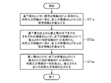
- FIG. 2 is a flowchart illustrating the distribution matching method according to the first embodiment.
- FIG. 3 is an image diagram showing an outline of the distribution matching method according to the first embodiment.
- the distribution matching method according to the first embodiment will be described with reference to the image shown in FIG.
- the number of layers of the LUT is Lm + 1, and Lm is an integer of 0 or more.
- the uppermost layer is the Lm layer, and the lowermost layer is the 0th layer.
- the 0th to M [Lm-1] LUTs belong to the (Lm-1) th layer, and the 0th to M [1] LUTs belong to the 1st layer. belong to.
- the 0th layer belongs to the 0th to M [0] th LUTs.
- LUT (Lm-1) -0 is the 0th LUT of the (Lm-1) th layer
- LUT0-M [0] is the Mth [0] th LUT of the 0th layer. .
- the LUT in the top layer converts a part of the external input information into specification information for specifying a combination of signal point groups in a signal space managed by each of the plurality of LUTs in the immediately lower layer, and converts the specification information to the immediately lower level.
- Output to each of the plurality of LUTs in the hierarchy (step ST1). This processing is "designation of the uppermost layer signal" in FIG.
- the LUT in the Lmth layer converts a part of the bit sequence of the external input information into a signal space set in the 0th to Mth [Lm-1] th LUTs in the (Lm-1) th layer.
- the signal point group designating bits are converted to signal point group designating bits, which are designation information for designating a point group combination, and the signal point group designating bits are output to each of the 0th to Mth [Lm-1] LUTs.
- the LUT of each layer from immediately below the uppermost layer to immediately above the lowermost layer converts a bit sequence composed of a part of the external input information and the designation information input from the LUT of the immediately upper layer into a plurality of bits of the immediately lower layer.
- the LUT is converted into designation information designating a combination of signal point groups in a signal space managed by each of the LUTs, and the designation information is output to each of a plurality of LUTs in the immediately lower hierarchy (step ST2). This process is "intermediate layer signal designation" in FIG.
- the LUTs from the 0th layer in the (Lm-1) th layer to the Mth [0] th layer in the first layer are composed of a part of the external input information and the signal point group designation bits input from the LUT in the immediately upper layer.
- the configured bit sequence is converted into signal point group designation bits, which are designation information for designating a combination of signal point groups in a signal space managed by each of the plurality of LUTs in the immediately lower hierarchy, and the signal point group designation bits are converted. Is output to each of a plurality of LUTs in the immediately lower hierarchy.
- Each of the lowermost LUTs converts a bit sequence composed of a part of the external input information and the designated information input from the LUT of the immediately upper layer into signal point information and outputs signal point information (step). ST3). This process is "designation of the lowest signal" in FIG.
- Each of the 0th to M [0] th LUTs in the 0th layer is composed of a part of external input information and signal point group designation bits input from the LUT in the first layer, which is the layer immediately above.
- the converted bit sequence is converted into signal point information, and the signal point information is output to the outside.
- the signal point information is information indicating the signal point arrangement in the signal space set in each of the 0th to Mth [0] th LUTs in the 0th layer, and is located downstream of the distribution matching circuit 1 in the optical transmitter. This is input information for the symbol mapping circuit to be arranged.
- a plurality of LUT output data hierarchized in a tree shape sequentially designates a combination of signal point groups in a signal space managed by the LUT of the immediately lower hierarchy. Then, signal point information after distribution matching is output for each LUT in the lowermost layer.
- the distribution matching circuit 1 may be configured to have only the uppermost layer LUT and the lowermost layer LUT shown in FIG. 1 without the intermediate layer LUT shown in FIG.
- the distribution matching circuit 1 includes a plurality of LUTs hierarchized into two layers.
- the upper-layer LUT 2-0 converts a part of the external input information into a combination of signal point groups in a signal space managed by each of the LUTs 4-0, LUT4-1, LUT4-2, and LUT4-3 belonging to the immediately lower layer.
- the specified information is converted to specified information, and the specified information is output to each of the LUTs 4-0, LUT4-1, LUT4-2, and LUT4-3 in the immediately lower layer.
- Each of the LUTs 4-0, LUT4-1, LUT4-2, and LUT4-3 in the lower layer represents a bit sequence composed of a part of the external input information and the designation information input from the LUT 2-0 in the immediately higher layer.
- the LUT 4-0, LUT4-1, LUT4-2, and LUT4-3 in the lowermost layer are converted into signal point information indicating a signal point arrangement in a signal space managed by each of the LUTs, and the signal point information is output.
- the specific operation of the LUT is the same as the operation described in the first embodiment.
- the distribution matching circuit 1 may not include the LUT of the uppermost layer and the LUT of the intermediate layer shown in FIG. 1 and may include only the LUT of the lowermost layer.
- the distribution matching circuit 1 includes LUT4-0, LUT4-1, LUT4-2 and LUT4-3 belonging to one layer.
- Each of the LUT4-0, LUT4-1, LUT4-2 and LUT4-3 of the layer has a part of the external input information and the LUT4-0, LUT4-1, LUT4-2 and LUT4-3 of the layer.
- Designation information for designating a combination of signal point groups in a signal space managed by each of them is input, and a bit sequence composed of a part of external input information and the designation information is converted into LUT4-0, LUT4- 1.
- the signal point information is converted to signal point information indicating the signal point arrangement in the signal space managed by each of the LUT 4-2 and the LUT 4-3, and the signal point information is output to the outside. Also in this configuration, the specific operation of the LUT is the same as the operation described in the first embodiment.
- FIG. 4 is a block diagram showing a configuration of the distributed matching termination circuit 5 according to the second embodiment.
- the distributed matching termination circuit 5 is provided in, for example, an optical receiving device, and performs distributed matching termination on signal point information included in a received signal received from the optical transmitting device, so that external input information input to the distributed matching circuit 1 is output. To restore.
- the distributed matching termination circuit 5 includes an LUT 6-0, LUT 6-1, LUT 6-2, LUT 6-3, LUT 7-0, LUT 7-1, and LUT 8-0. These LUTs are hierarchized in a tree shape, and data associated with addresses is registered in each LUT.
- FIG. 4 illustrates a distributed matching termination circuit 5 having LUTs hierarchized into three layers.
- the number of layers of the LUT may be two or less or four or more as long as the number of layers is the same as that of the distribution matching circuit 1.
- LUT 6-0, LUT 6-1, LUT 6-2, and LUT 6-3 are LUTs in the 0th layer, which is the lowest layer.
- the LUTs 7-0 and 7-1 are LUTs of the first layer which is an intermediate layer.
- the LUT 7-0 is connected to the LUT 6-0 and the LUT 6-1 in the immediately lower hierarchy, and the LUT 7-1 is connected to the LUT 6-2 and the LUT 6-3 in the immediately lower hierarchy.
- the LUT 8-0 is a second-layer LUT that is the uppermost layer. To the LUT 8-0, the LUT 7-0 and the LUT 7-1 in the immediately lower hierarchy are connected.
- LUT6-0, LUT6-1, LUT6-2, LUT6-3, LUT7-0, LUT7-1, and LUT8-0 each manage a signal space.
- the signal space managed by the LUT 6-0 is the space (S0) of two QAM signals
- the signal space managed by the LUT 6-1 is the space (S1) of another two QAM signals
- the LUT 6- 2 is a space (S2) for another two QAM signals
- a signal space managed by the LUT 6-3 is a space (S3) for another two QAM signals.
- the signal space managed by the LUT 7-0 is the signal spaces S0 and S1 managed by the LUT 6-0 and the LUT 6-1.
- the signal space managed by the LUT 7-1 is managed by the LUT 6-2 and the LUT 6-3.
- the signal spaces managed by the LUT 8-0 are the signal spaces S0, S1, S2 and S3 managed by the LUTs 7-0 and 7-1.
- a signal point is a point of a complex amplitude value in a signal space diagram.
- LUT 6-0, LUT6-1, LUT6-2, and LUT6-3 Signal point information from the LUTs 4-0, LUT4-1, LUT4-2, and LUT4-3 in the distribution matching circuit 1 is input to the LUT 6-0, LUT6-1, LUT6-2, and LUT6-3.
- the LUT 6-0 and the LUT 6-1 are based on the bit sequence of the signal point information, from a part of the external input information input to the LUT 4-0 and the LUT 4-1 in the distribution matching circuit 1, and from the LUT 3-0 of the immediately higher layer. And restore the specified information.
- the LUT 6-2 and the LUT 6-3 are based on the bit sequence of the signal point information, from a part of the external input information input to the LUT 4-2 and the LUT 4-3 in the distribution matching circuit 1, and from the LUT 3-1 in the immediately higher layer. And restore the specified information.
- the LUT 7-0 of the first layer which is the intermediate layer, uses a part of the external input information in the distribution matching circuit 1 and the LUT 7-0 of the second layer from the bit sequence of the designated information restored by the LUT 6-0 and the LUT 6-1 immediately below.
- the designated information from the LUT 2-0 is restored.
- the first layer LUT 7-1 is obtained from the bit sequence of the designated information restored by the LUT 6-2 and the LUT 6-3, from the external input part in the distribution matching circuit 1 and the second layer LUT 2-0. And restore the specified information.
- the LUT 8-0 of the second layer which is the uppermost layer, is input to the LUT 2-0 of the second layer in the distribution matching circuit 1 from the bit sequence of the designated information restored by the LUT 7-0 of the immediately lower layer and the LUT 7-1. A part of the restored external input information is restored, and all the restored external input information is output to the outside.
- the number of bits output in one clock cycle is usually smaller than the number of bits input in one clock cycle.
- distribution matching is terminated for a bit sequence obtained by demapping a signal that is made redundant by distribution matching and has a bias in the probability distribution of signal points modulated by QAM or the like, and an information bit sequence to be communicated is restored.
- the information bit sequence to be communicated corresponds to external input information in distribution matching, and is usually a bit sequence having a mark rate of about 0.5 and having no temporal correlation.
- the number of branches between layers is two, but the number of branches may be any positive integer.
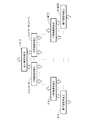
- FIG. 5 is a flowchart showing a distributed matching termination method according to the second embodiment.
- FIG. 6 is an image diagram showing an outline of the distributed matching termination method according to the second embodiment.
- the distributed matching termination method according to the second embodiment will be described with reference to the image shown in FIG.
- the number of layers of the LUT is Lm + 1, and Lm is an integer of 0 or more.
- the uppermost layer is the Lm layer, and the lowermost layer is the 0th layer.
- the 0th to Mth [Lm-1] LUTs belong, and in the 1st layer, the 0th to Mth [1] LUTs. belong to.
- the 0th layer belongs to the 0th to M [0] th LUTs.
- LUT (Lm-1) -0 is the 0th LUT of the (Lm-1) th layer
- LUT0-M [0] is the Mth [0] th LUT of the 0th layer. .
- Each of the plurality of LUTs belonging to the lowermost layer is output from the distribution matching circuit 1 and, based on the bit sequence of the signal point information obtained via an arbitrary communication propagation path, from the external input information and the LUT of the immediately upper layer Is restored (step ST1a).
- This process is the “restoration of lowermost layer signal” in FIG.
- the communication channel includes a symbol mapping circuit on the transmitting side and a symbol demapping circuit on the receiving side.
- Each of the 0th to M [0] th LUTs in the 0th layer converts a bit sequence constituting the signal point information into a signal in a signal space managed by the 1st layer LUT, which is a layer immediately above.
- This conversion processing is performed by table lookup.
- the input to the LUT corresponds to an address
- the output from the LUT corresponds to data.
- the relationship between address and data usually corresponds one-to-one.
- Part of the restored data of the external input information is obtained by restoring the external input information input to the 0th layer LUT in the distribution matching circuit 1.
- the LUT of each layer from immediately above the lowermost layer to immediately below the uppermost layer is obtained by extracting a part of the external input information from the bit sequence of the designated information restored by the LUT of the immediately lower layer and the LUT from the LUT of the immediately upper layer.
- the designated information is restored (step ST2a). This process is "intermediate layer signal restoration" in FIG.
- the LUTs from the 0th layer in the first layer to the Mth [Lm-1] th layer in the (Lm-1) th layer represent bit sequences constituting signal point group designation bits restored by the LUTs in the immediately lower layer, Restoration of signal point group designation bits by converting into signal point group designation bit restoration data that designates a combination of signal point groups in the signal space of the LUT of the immediately higher hierarchy and restoration data of a part of external input information
- the data is output to the LUT at the immediately upper layer, and a part of the restored data of the external input information is output to the outside.
- a part of the restored data of the external input information is obtained by restoring the external input information input to the corresponding LUT of the first layer to the (Lm-1) th layer in the distribution matching circuit 1.
- the LUT in the uppermost layer restores a part of the external input information in the distribution matching circuit 1 from the bit sequence of the designated information restored in the LUT in the immediately lower layer, and outputs all the restored external input information to the outside.
- Output step ST3a.
- This process is the uppermost layer signal restoration in FIG.
- the LUT in the Lm-th layer converts the signal point group designation bits input from the 0th to Mth [Lm-1] th LUTs in the (Lm-1) th layer into restored data of a part of the external input information. After conversion, a part of the restored data of the external input information is output to the outside.
- This external input information is obtained by restoring the external input information input to the LUT of the Lm-th layer in the distribution matching circuit 1.
- the plurality of LUTs hierarchized in a tree form is a part of the external input information input to the LUT of the corresponding hierarchy in the distributed matching circuit 1.
- the LUT of the uppermost layer restores and outputs the external input information input to the LUT of the corresponding layer in the distribution matching circuit 1. Since a plurality of hierarchized LUTs are used, it is not necessary to perform integer multiplication or integer addition many times in order at the distribution matching termination, and it is not necessary to implement a plurality of arithmetic circuits in parallel. Thereby, the circuit scale and power consumption of the distributed matching termination circuit can be reduced.
- the external input information in the distribution matching circuit 1 can be partially restored, so that the number of errors in the signal after termination of the distribution matching does not become significant. For this reason, in the related art, error correction of the signal after the termination of the distributed matching is impossible, but error correction of the signal after the termination of the distributed matching by the distributed matching termination circuit 5 is possible.
- the distribution matching circuit 1 includes a processing circuit for executing the processing from step ST1 to step ST3 shown in FIG.
- the distributed matching termination circuit 5 includes a processing circuit for executing the processing from step ST1a to step ST3a shown in FIG.
- the processing circuit may be dedicated hardware, or may be a CPU (Central Processing Unit) that executes a program stored in the memory.
- CPU Central Processing Unit
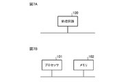
- FIG. 7A is a block diagram showing a hardware configuration for realizing the function of the distributed matching circuit 1 or the distributed matching termination circuit 5.
- FIG. 7B is a block diagram illustrating a hardware configuration that executes software for realizing the functions of the distributed matching circuit 1 or the distributed matching termination circuit 5.
- the processing circuit is the dedicated hardware processing circuit 100 illustrated in FIG. 7A
- the processing circuit 100 includes, for example, a single circuit, a composite circuit, a programmed processor, a parallel programmed processor, and an ASIC (Application Specific Integrated). Circuit, FPGA (Field-Programmable Gate Array), or a combination thereof.
- the function of the LUT in the distributed matching circuit 1 or the function of the LUT in the distributed matching termination circuit 5 may be realized by separate processing circuits, or these functions may be realized by a single processing circuit.
- the processing circuit is the processor 101 shown in FIG. 7B
- the function of the LUT in the distributed matching circuit 1 or the function of the LUT in the distributed matching termination circuit 5 is realized by software, firmware, or a combination of software and firmware.
- the software or firmware is described as a program and stored in the memory 102.
- the processor 101 implements the function of the LUT in the distributed matching circuit 1 or the function of the LUT in the distributed matching termination circuit 5 by reading and executing the program stored in the memory 102. That is, the distribution matching circuit 1 includes a memory 102 for storing a program that, when executed by the processor 101, results in the processing of steps ST1 to ST3 shown in FIG. Similarly, the distributed matching termination circuit 5 includes a memory 102 for storing a program that, when executed by the processor 101, results in the processing from step ST1a to step ST3a shown in FIG.
- the memory 102 may be a computer-readable storage medium in which a program for causing a computer to function as the LUT in the distributed matching circuit 1 or the LUT in the distributed matching termination circuit 5 is stored.
- the memory 102 includes, for example, a RAM (Random Access Memory), a ROM (Read Only Memory), a flash memory, an EPROM (Erasable Programmable Read Only Memory), a nonvolatile semiconductor memory such as an EEPROM (Electrically-EROM), or the like.
- RAM Random Access Memory
- ROM Read Only Memory
- flash memory an EPROM (Erasable Programmable Read Only Memory)
- nonvolatile semiconductor memory such as an EEPROM (Electrically-EROM), or the like.
- a magnetic disk, a flexible disk, an optical disk, a compact disk, a mini disk, a DVD, and the like are applicable.
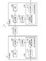
- FIG. 8 is a block diagram illustrating a configuration of the optical transmission system 9 according to the third embodiment.
- the optical transmission system 9 includes an optical transmission device 10, an optical reception device 11, and an optical transmission line 12.
- the optical transmission device 10 outputs an optical signal obtained by encoding external input information to the optical transmission line 12.
- the external input information is a client signal or a frame signal. That is, the optical transmission device 10 generates an optical signal obtained by encoding a client signal or a frame signal, and outputs the optical signal to the optical transmission line 12.
- the optical receiver 11 decodes external input information based on the optical signal received via the optical transmission line 12. For example, the optical receiver 11 converts an optical signal received from the optical transmitter 10 into a client signal or a frame signal and outputs the converted signal to the outside.
- the optical transmission line 12 is a transmission line for transmitting an optical signal from the optical transmission device 10 to the optical reception device 11, and includes, for example, an optical fiber, an optical amplifier, a wavelength multiplexer, a wavelength separator, an optical power monitor, and a wavelength selection device. It has a switch.
- the optical transmission device 10 includes a transmission signal processing circuit 1100, a DA converter 1200, a light source 1300, and an optical modulator 1400.
- the transmission signal processing circuit 1100 performs signal processing on a client signal or a frame signal, which is external input information, and outputs the result to the DA converter 1200.
- the transmission signal processing circuit 1100 includes an encoding circuit 1110 and a transmission signal compensation processing circuit 1120.
- the encoding circuit 1110 performs an encoding process on the client signal or the frame signal input from the outside, and outputs the signal after the encoding process to the transmission signal compensation processing circuit 1120.
- the transmission signal compensation processing circuit 1120 performs signal spectrum shaping and non-linear response compensation for the optical transmission device 10 on the encoded signal input from the encoding circuit 1110, and converts the compensated signal into a DA converter. 1200.
- the DA converter 1200 performs digital-to-analog conversion processing and electrical amplification on the digital signal input from the transmission signal processing circuit 1100, and outputs the digital signal to the optical modulator 1400.
- the light source 1300 is a transmission light source that generates continuous light and outputs the light to the optical modulator 1400.
- the continuous light is, for example, continuous light oscillated at a wavelength of 1550 nm.
- the optical modulator 1400 modulates continuous light input from the light source 1300 with an electric signal input from the DA converter 1200 and outputs the modulated optical signal to the optical transmission line 12.
- the optical modulator 1400 for example, a polarization multiplexing Mach-Zehnder type quadrature optical modulator using lithium niobate is used.
- the optical receiver 11 includes a received signal processing circuit 2100, an AD converter 2200, a light source 2300, and an optical receiver 2400, as shown in FIG.
- the light source 2300 is a local oscillation light source that generates continuous light and outputs it to the optical receiver 2400.
- the continuous light is, for example, continuous light oscillated at a wavelength of 1550 nm.
- the optical receiver 2400 causes the optical signal received from the optical transmitter 10 via the optical transmission line 12 to interfere with the continuous light input from the light source 2300, and photoelectrically converts the optical signal to the AD converter 2200. Output.
- a polarization phase diversity type coherent receiver is used as the optical receiver 2400.
- the AD converter 2200 amplifies the electric signal input from the optical receiver 2400, performs analog-to-digital conversion, and outputs the result to the reception signal processing circuit 2100.
- the received signal processing circuit 2100 restores a client signal or a frame signal, which is external input information, based on the digital signal input from the AD converter 2200, and outputs the same to the outside.
- the received signal processing circuit 2100 includes a decoding circuit 2110 and a received signal compensation processing circuit 2120.
- the received signal compensation processing circuit 2120 performs sampling phase synchronization, waveform equalization, restoration of carrier frequency and phase on the digital signal input from the AD converter 2200, and outputs the digital signal to the decoding circuit 2110.
- the decoding circuit 2110 performs a decoding process on the digital signal input from the received signal compensation processing circuit 2120, and outputs the restored client signal or frame signal to the outside.
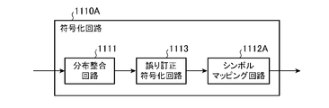
- FIG. 9 is a block diagram showing a configuration of the encoding circuit 1110 of FIG.
- the encoding circuit 1110 includes a distribution matching circuit 1111 and a symbol mapping circuit 1112, as shown in FIG.
- the distribution matching circuit 1111 is the distribution matching circuit 1 described in the first embodiment.
- the distribution matching circuit 1111 receives a client signal or a frame signal as external input information, performs the distribution matching described in the first embodiment, and performs the distribution matching.
- the obtained signal point information is output to symbol mapping circuit 1112.
- the symbol mapping circuit 1112 converts the signal point information input from the distribution matching circuit 1111 into a modulation symbol, and outputs the modulation symbol to the transmission signal compensation processing circuit 1120.
- the symbol mapping circuit 1112 combines signal point information from the LUT in the lowermost layer of the distribution matching circuit 1111 by 3 bits to generate a single-sided pulse amplitude modulation symbol having an 8-level amplitude.
- the eight amplitude values are -7, -5, -3, -1, 1, 3, 5, and 7. At this time, if the amplitude value differs by one stage, a Gray code in which the input bits differ by one bit is used.
- the signal point information output from each of the LUTs 4-0, LUT4-1, LUT4-2, and LUT4-3 of the 0th layer which is the lowermost layer is, for example, , May be sorted into a list under the following conditions.
- the listed signal point information is associated with the address with the smallest address.
- Sorting is performed in ascending order of modulation symbol power defined after signal point information is converted into modulation symbols by the symbol mapping circuit 1112.
- Sorting is performed in descending order of the number of 0s included in the signal point information.
- the LUT belonging to the layer immediately above may limit the table lookup in the LUT belonging to the layer immediately below.
- the first layer LUT imposes restrictions on table lookup in the zeroth layer LUT.
- “Constraining the table lookup” means specifying a signal point group that can be taken in the signal space.
- the signal point group designating bits output from the LUT belonging to the immediately higher hierarchy to the LUT belonging to the immediately lower hierarchy are sorted under the following conditions.
- the sorted signal point group designation bits are associated with the address having the smaller address.
- Sorting is performed in ascending order of expected modulation symbol power values defined after the signal point information is converted into modulation symbols by the symbol mapping circuit 1112.
- the modulation symbol obtained by inputting the signal point information generated by defining the address-data relationship of the LUT to the symbol mapping circuit 1112 as described above has, for example, a high probability of taking a signal point with a small power and a large signal with a large power.
- the bias is such that the probability of taking a signal point is low.
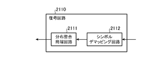
- FIG. 10 is a block diagram showing a configuration of the decoding circuit 2110 in FIG.
- the decoding circuit 2110 includes a distribution matching termination circuit 2111 and a symbol demapping circuit 2112 as shown in FIG.
- the symbol demapping circuit 2112 generates a soft decision likelihood or performs a hard decision on the digital signal input from the received signal compensation processing circuit 2120.
- the soft decision likelihood is the received bit likelihood
- the hard decision value is a received bit sequence.
- the symbol demapping circuit 2112 considers the occurrence probability of the modulation symbol generated by the encoding circuit 1110. For example, when outputting a soft decision value, the log posterior probability ratio (posterior L-value) is represented by three or more values, and when performing a hard decision, the hard decision value is represented by a binary value (1 bit). The likelihood or hard decision value obtained by the symbol demapping circuit 2112 is output to the distribution matching termination circuit 2111.
- the log posterior probability ratio posterior L-value
- the hard decision value is represented by a binary value (1 bit).
- the distributed matching termination circuit 2111 is the distributed matching termination circuit 5 described in the second embodiment.
- the distributed matching termination circuit 2111 performs the distributed matching termination described in Embodiment 2 on the signal input from the symbol demapping circuit 2112, and outputs a client signal or a frame signal restored by the distributed matching termination to the outside.
- the number of input / output bits of the LUT needs to be paired between the distributed matching circuit 1111 included in the optical transmitting device 10 and the distributed matching termination circuit 2111 included in the optical receiving device 11.
- the distributed matching circuit 1111 is the distributed matching circuit 1 shown in FIG. 1
- the distributed matching terminal circuit 2111 is the distributed matching terminal circuit 5 shown in FIG.
- the number of input bits of the 0th LUT 3-0 is equal to the number of output bits of the same number (0th) LUT 7-0 of the first layer in the distributed matching termination circuit 5.
- the number of output bits of the 0th LUT 3-0 of the first layer is equal to the number of input bits of the same numbered LUT 7-0 of the first layer.
- the number of information bits and the number of signal point group designation bits included in the input or output bits of the 0th LUT 3-0 in the first layer are equal to the same number of LUTs 7-0 in the first layer. . These relationships are common to the LUTs of the corresponding layers in the distributed matching circuit 1 and the distributed matching termination circuit 5.
- the relationship between the address and the data is reversed between the LUT included in the distribution matching circuit 1111 and the LUT included in the distribution matching termination circuit 2111.
- the distributed matching circuit 1111 is the distributed matching circuit 1 shown in FIG. 1
- the distributed matching termination circuit 2111 is the distributed matching termination circuit 5 shown in FIG. 4
- the LUT 3-0 of the first layer If the first address specifies the first data, the corresponding first layer LUT 7-0 has the first address, the second address, and the first address, the second address, in the corresponding first layer LUT 7-0. Data is specified.
- the LUT 3-0 designates the signal point group designating bit as the first data by the first address composed of the information bits of the external input information and the signal point group designating bit inputted from the LUT of the immediately upper layer.
- the first data is specified as the second address
- the second data is specified.
- parameters may be selected such that the number of output bits is larger than the number of input bits.
- the LUT included in the distributed matching circuit 1111 is a transmission LUT and the LUT included in the distributed matching termination circuit 2111 is a reception LUT, if the transmission LUT has more output bits than input bits. , The number of bits of the address of the LUT is larger in the receiving LUT than in the transmitting LUT. Therefore, there is a possibility that the LUT on the receiving side has an address that does not exist in the LUT on the transmitting side.
- the output data of the transmitting LUT completely corresponds to the address of the paired receiving LUT. This does not mean that an error remains in the signal to be transmitted.
- the relationship between the address and the data that does not exist in the transmitting LUT is defined by the receiving LUT. That is, the address list of the distributed matching circuit 1111 is used as the data list of the distributed matching termination circuit 2111, and at least the data list of the distributed matching circuit 1111 is used as the address list of the distributed matching circuit 2111.
- the data corresponding to the address not included in the data list on the circuit 1111 side may be selected from the address list on the distributed matching termination circuit 2111 side while allowing duplication.
- the circuit mounting can be simplified.
- the received signal compensation processing circuit 2120 operates the equalizer and the carrier recovery circuit based on the known signal (for example, a pilot signal).
- the conditions (1), (2), and (3) above can greatly reduce the number of address-data relationship combinations stored in the LUT. As a result, the capacity of the original data that holds the address-data relationship can be reduced, writing to the LUT can be performed at the same time, and the time required for writing the LUT can be reduced. In addition, by sharing the interface conditions of the LUT, the designed circuit can be reused.
- the condition (4) directly contributes to the reduction in the size of each LUT. When the number of input bits of the LUT is increased, the number of addresses increases exponentially. Therefore, the LUT is hierarchized to reduce the number of input bits per one.
- the number of input bits on the distribution matching side corresponds to the number of output bits on the distribution matching termination side
- the number of output bits on the distribution matching side corresponds to the number of input bits on the distribution matching termination side. It is desirable to keep the number of output bits small.
- the condition (5) is that, even if the signal point arrangement or the occurrence probability of each signal point is flexibly changed, it is desirable that the recovery processing of various signals operates normally. This corresponds to the fact that processing that can operate independently of conditions is more desirable.
- the distribution matching circuit 1111 may have a configuration in which a plurality of transmission systems, which are a plurality of LUTs hierarchized in a tree shape, are arranged in parallel.
- the distributed matching termination circuit 2111 may have a configuration in which a plurality of reception systems, which are a plurality of LUTs hierarchized in a tree shape, are arranged in parallel.
- a clock cycle may be provided in which a main signal is not input, that is, input data is undefined.
- the main signal is a client signal or a frame signal.
- the circuit is operated at a frequency 1% faster than the operating frequency of the main signal, and while the main signal is input for 100 clock cycles, the input of the main signal is not performed for one clock cycle.
- the contents of the LUT may be updated in one clock cycle.
- the external input information may include both valid bits constituting information and invalid bits not constituting information.
- the optical transmission system 9 external input information obtained by rearranging valid bits and invalid bits upstream of the distribution matching circuit 1111 is input to the distribution matching circuit 1111. Further, the valid bits and the invalid bits of the external input information restored by the distributed matching termination circuit 2111 are rearranged downstream of the distributed matching termination circuit 2111.
- the symbol rate of the electric signal for driving the optical modulator 1400 may be, for example, 64 Gsymbol / s.
- the optical transmission device 10 includes the distribution matching circuit 1111 and the symbol mapping circuit 1112, and the optical reception device 11 includes the symbol demapping circuit 2112. , A distributed matching termination circuit 2111.
- the optical transmission system 9 can obtain the effects described in the first and second embodiments.
- FIG. 11 is a block diagram showing a configuration of an encoding circuit 1110A according to Embodiment 4. 11, the same components as those in FIG. 9 are denoted by the same reference numerals, and detailed description will be omitted.
- the encoding circuit 1110A is provided instead of the encoding circuit 1110 in the optical transmission device 10 shown in FIG.
- FIG. 12 is a block diagram showing a configuration of a decoding circuit 2110A according to the fourth embodiment. 12, the same components as those in FIG. 10 are denoted by the same reference numerals, and detailed description will be omitted.
- the decoding circuit 2110A is provided instead of the decoding circuit 2110 in the optical receiver 11 shown in FIG.
- the encoding circuit 1110A includes a distribution matching circuit 1111, a symbol mapping circuit 1112A, and an error correction encoding circuit 1113.
- Error correction coding circuit 1113 performs systematic error correction coding on the signal point information input from distribution matching circuit 1111 and outputs error correction information bits and error correction parity bits to symbol mapping circuit 1112A.
- the distribution matching circuit 1111 may use a signal output to the error correction encoding circuit 1113 in a frame format in which an error correction parity area is reserved in advance.
- Symbol mapping circuit 1112A generates a modulation symbol based on the error correction information bits and error correction parity bits input from error correction encoding circuit 1113, and outputs the modulation symbol to transmission signal compensation processing circuit 1120.
- the mark rate of error correction parity bits cannot be controlled (around 0.5), and stochastic shaping cannot be performed.
- the symbol mapping circuit 1112A assigns the error correction parity bits as code bits for controlling the positive and negative polarities of the modulation symbol. For example, in a single-sided pulse amplitude modulation symbol having an 8-level amplitude, the number of bits (so-called amplitude bits) affecting the amplitude of the modulation symbol is 2 bits.
- the symbol mapping circuit 1112A allocates parity bits while maintaining the combination of the two bits. However, when these restrictions cannot be satisfied, for example, error correction parity bits may be assigned to amplitude bits, or amplitude bits that are distributed and matched may be assigned to code bits.
- the decoding circuit 2110A includes a distributed matching termination circuit 2111A, a symbol demapping circuit 2112, and an error correction decoding circuit 2113.
- Error correction decoding circuit 2113 performs error correction decoding on the signal input from symbol demapping circuit 2112, and outputs the corrected error correction information bits to distribution matching termination circuit 2111A.
- the distributed matching termination circuit 2111A performs the distributed matching termination described in Embodiment 2 on the signal input from the error correction decoding circuit 2113, and outputs the restored client signal or frame signal to the outside. Further, the distributed matching termination circuit 2111A may treat the signal input from the error correction decoding circuit 2113 as a signal in a frame format in which an error correction parity area is reserved in advance.
- bits may be rearranged between the distribution matching circuit 1111 and the error correction coding circuit 1113.
- a low-density parity check code used for error correction coding has different levels of correction capability in a code space. For this reason, there is a case where a bit having lower performance among the modulation bits is arranged on a side having a higher correction ability, and a bit having higher performance among the modulation bits is arranged on a side having a lower correction ability.
- three bits are assigned to one 8-amplitude pulse amplitude modulation symbol, and performance differs between the bits. In this case, there are three bit levels.
- Bit level allocation to the error correction code space is called bit level mapping.
- the bit level mapping performed between the distribution matching circuit 1111 and the error correction encoding circuit 1113 is restored between the error correction decoding circuit 2113 and the distribution matching termination circuit 2111A. This process is called bit-level demapping.
- the encoding circuit 1110A according to Embodiment 4 includes the error correction encoding circuit 1113, and the symbol mapping circuit 1112A converts the signal point information encoded by the error correction encoding circuit 1113. Convert to modulation symbols.
- the decoding circuit 2110A according to the fourth embodiment includes an error correction decoding circuit 2113, and the distributed matching termination circuit 2111A restores external input information based on the result of the error correction decoding performed by the error correction decoding circuit 2113.
- the decoding circuit 2110A according to Embodiment 4 can partially decode even if an error remains in the signal input to the distributed matching termination circuit 2111A. Thereby, it is possible to correct the error remaining in the signal.
- FIG. 13 is a block diagram showing a configuration of an encoding circuit 1110B according to Embodiment 5. 13, the same components as those in FIG. 9 are denoted by the same reference numerals, and detailed description will be omitted.
- the encoding circuit 1110B is provided instead of the encoding circuit 1110 in the optical transmission device 10 illustrated in FIG.
- FIG. 14 is a block diagram showing a configuration of a decoding circuit 2110B according to the fifth embodiment. 14, the same components as those in FIG. 10 are denoted by the same reference numerals, and detailed description will be omitted.
- the decoding circuit 2110B is provided instead of the decoding circuit 2110 in the optical receiver 11 shown in FIG.
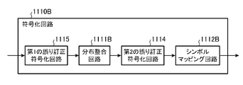
- the encoding circuit 1110B includes a distribution matching circuit 1111B, a symbol mapping circuit 1112B, a second error correction encoding circuit 1114, and a first error correction encoding circuit 1115.
- the first error correction encoding circuit 1115 performs arbitrary error correction encoding on a client signal or a frame signal input from the outside, and outputs encoded bits to the distribution matching circuit 1111B.
- the error correction information bits obtained by the error correction encoding by the first error correction encoding circuit 1115 are called outer code error correction information bits.
- the distribution matching circuit 1111B performs the distribution matching described in the first embodiment on the signal input from the first error correction coding circuit 1115, and converts the signal point information obtained by the distribution matching into the second error. Output to the correction encoding circuit 1114.
- Second error correction coding circuit 1114 performs systematic error correction coding on the signal point information input from distribution matching circuit 1111B, and outputs error correction information bits and error correction parity bits to symbol mapping circuit 1112B. I do. Note that the error correction information bits and the error correction parity bits obtained by the error correction coding by the second error correction coding circuit 1114 are called inner code error correction information bits and inner code error correction parity bits.
- the symbol mapping circuit 1112B generates a modulation symbol based on the inner code error correction information bits and the inner code error correction parity bits input from the second error correction encoding circuit 1114, and outputs the modulation symbol to the transmission signal compensation processing circuit 1120. .
- the symbol mapping circuit 1112B sets the inner code error correction parity bit as a code bit for controlling the positive / negative polarity of the modulation symbol. Assign parity bits.
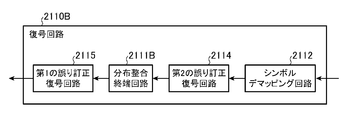
- the decoding circuit 2110B includes a distribution matching termination circuit 2111B, a symbol demapping circuit 2112, a second error correction decoding circuit 2114, and a first error correction decoding circuit 2115.
- Second error correction decoding circuit 2114 performs error correction decoding on the signal input from symbol demapping circuit 2112, and outputs the error correction information bits obtained by the error correction decoding to distribution matching termination circuit 2111B.
- the error correction information bits obtained by the error correction decoding by the second error correction decoding circuit 2114 are called inner code error correction information bits.
- the distributed matching termination circuit 2111B performs the distributed matching termination described in the second embodiment on the inner code error correction information bits input from the second error correction decoding circuit 2114 and restores the client signal or the client signal restored by the distributed matching termination.
- the frame signal is output to first error correction decoding circuit 2115.
- First error correction decoding circuit 2115 performs error correction decoding on the signal input from distributed matching termination circuit 2111B, and outputs the obtained error correction information bits to the outside as a restored client signal or frame signal.
- the error correction information bits obtained by the error correction decoding by the first error correction decoding circuit 2115 are called outer code error correction information bits.
- the coding circuit 1110B includes the first error correction coding circuit 1115 and the second error correction coding circuit 1114.
- the distribution matching circuit 1111B inputs the external input information error-correction-coded by the first error correction coding circuit 1115 and outputs signal point information, and the symbol mapping circuit 1112B generates the second error-correction coding circuit.
- the signal point information that has been error-correction coded by 1114 is converted into a modulation symbol.
- the decoding circuit 2110B according to the fifth embodiment includes a first error correction decoding circuit 2115 and a second error correction decoding circuit 2114.
- the distributed matching termination circuit 2111B restores the external input information based on the inner code error correction information bits obtained by the second error correction decoding circuit 2114.
- the external input information output from the distributed matching termination circuit 2111B is subjected to error correction decoding by a first error correction decoding circuit 2115, and the outer code error correction information bits are output to the outside as restored external input information.
- the required SNR can be reduced by, for example, 0.3 to 1.1 dB.
- the circuit resources required for the distributed matching circuit and the distributed matching termination circuit are a small-sized RAM or ROM for LUT, a flip-flop and a selector for delay adjustment, and add processing and multiplication requiring bit precision. No processing is required. Thereby, it is not necessary to mount a plurality of arithmetic circuits in parallel, and it is possible to reduce the circuit scale and power consumption of the distributed matching circuit. It is also useful for large-capacity optical transmission.
- the distribution matching circuit according to the present invention can be used for an optical transmission device of an optical transmission system because the circuit scale can be reduced.
- 1,1111,1111B distribution matching circuit 1,1111,1111B distribution matching circuit, 2-0,3-0,3-1,4-0,4-1,4-2,4-3,6-0,6-1,6-2,6 -3, 7-0, 7-1, 8-0 look-up table (LUT), 5, 211, 1111A, 2111B distributed matching termination circuit, 9 optical transmission system, 10 optical transmitter, 11 optical receiver, 12 optical Transmission line, 100 processing circuit, 101 processor, 102 memory, 1100 transmission signal processing circuit, 1110, 1110A, 1110B coding circuit, 1112, 1112A, 1112B symbol mapping circuit, 1113 error correction coding circuit, 1114 second error correction Coding circuit, 1115 first error correction coding circuit, 1120 transmission signal compensation processing circuit, 1200 DA converter, 1300, 300 light source, 1400 light modulator, 2100 reception signal processing circuit, 2110, 2110A, 2110B decoding circuit, 2112 symbol demapping circuit, 2113 error correction decoding circuit, 2114 second error correction decoding circuit, 2115 first error correction decoding Circuit
Landscapes
- Engineering & Computer Science (AREA)
- Computer Networks & Wireless Communication (AREA)
- Signal Processing (AREA)
- Physics & Mathematics (AREA)
- Electromagnetism (AREA)
- Optical Communication System (AREA)
Abstract
分布整合回路(1)において、ツリー状に階層化された複数のLUT出力データが、直下の階層のLUTが管理する信号空間における信号点群の組み合わせを順次指定し、最下層でLUTごとに分布整合後の信号点情報を出力する。
Description
本発明は、通信に用いる信号点配置の確率的整形を行う分布整合回路、分布整合終端回路、分布整合方法、分布整合終端方法、および、それらを用いた光伝送システムに関する。
光通信で高いスループットを実現するためには、例えば、変調多値度を増加させることが有効である。変調多値度を増加させる場合、信号通信の送信側では直交振幅変調(Quadrature Amplitude Modulation;以下、QAMと記載する)を行い、受信側ではコヒーレント検波およびデジタル信号処理を行うことが通常である。
一方、QAM信号に載せるビット数を増加させると、信号点の数も増加し、信号の平均電力に対する信号点間の最小距離が縮小していく。これによって、一定の通信品質を得るために必要な信号対雑音比(Signal-to-Noise Ratio;以下、SNRと記載する)が増加し、適用可能な伝送条件が制限される。
光通信では誤り率の許容値が非常に小さいケースが多く、ハイエンドの機器において、誤り訂正を行うことが通常である。特に、性能を重視する場合、軟判定誤り訂正が用いられる。これまで多値QAMと軟判定誤り訂正との組み合わせが検討されてきたが、さらに確率的整形(Probabilistic Shaping)を組み合わせることが検討されている。
信号点の配置を整形する技術には、複数の信号点のそれぞれの位置を整形する幾何的整形(Geometric Shaping)と、複数の信号点のそれぞれがとり得る確率を整形する確率的整形(Probabilistic Shaping)とが存在する。いずれであってもSNRに対する伝送容量の関係をシャノン限界に漸近させることが可能である。これは、例えば、与えられた伝送条件において、クライアント信号の通信容量を増加させることに寄与する。
例えば、非特許文献1には、確率的整形と誤り訂正とを組み合わせた方法が記載されている。この方法では、確率的整形における送信側の処理である分布整合(Distribution Matching;DM)を誤り訂正符号化よりも上流で行い、組織的(システマティック)な誤り訂正処理を仮定して、受信側の処理である分布整合終端(Distribution DeMatching;invDM)を誤り訂正復号よりも下流で行っている。ここでいう「整合」は、あるSNRをもつガウシアンチャネルへの、通信信号の整合を意味する。理想的に整合させることは極めて困難であるため、実際に行われる処理は、送信信号の平均電力に対する信号点間の最小距離を可能な限り拡大させることに概ね等価である。
非特許文献1に記載された方法において、確率的整形における分布整合および分布整合終端には、非特許文献2に記載される同一組成分布整合(Constant Composition DM)または非特許文献3に記載されるn中のmコード(m-out-of-n Code)が用いられる。
G. Bocherer, P. Schulte and F. Steiner, "Bandwidth Efficient and Rate-Matched Low-Check Coded Modulation", IEEE Transactions on Communications, vol.63, no. 12, pp. 4651-4665, December 2015.
P. Schulte and G. Bocherer, "Constant Composition Distribution Matching", IEEE Transactions on Information Theory, vol. 62, no. 1, pp. 430-434, January 2016.
T. V. Ramabadran, "A Coding Scheme for m-out-of-n Codes", IEEE Transactions on Communications, vol. 38, no. 8, pp. 1156-1163, August 1990.
非特許文献2および非特許文献3に記載される分布整合および分布整合終端では、整数乗算または整数加算を順序立てて多数回行う必要があり、個々の演算回路の規模が大きいだけでなく実行速度が遅い。実行速度に起因した処理の遅延を低減するには複数の演算回路を並列実装する必要がある。そのため、分布整合回路および分布整合終端回路の回路規模が非常に大きいという課題があった。
本発明は上記課題を解決するものであって、回路規模を低減することができる分布整合回路および分布整合終端回路を得ることを目的とする。
本発明に係る分布整合回路および分布整合終端回路は、それぞれツリー状に階層化された複数のルックアップテーブルを備える。分布整合回路の最上層のルックアップテーブルは、外部からクライアント信号またはフレーム化された信号として入力される通信対象の情報(外部入力情報)の一部を、直下の階層の複数のルックアップテーブルのそれぞれが管理する信号空間での信号点群の組み合わせを指定する指定情報に変換して、指定情報を直下の階層の複数のルックアップテーブルのそれぞれに出力し、最上層の直下から最下層の直上までのそれぞれの階層のルックアップテーブルは、外部入力情報の一部と直上の階層に属するルックアップテーブルから入力した指定情報とにより構成されるビット系列を、直下の階層の複数のルックアップテーブルのそれぞれが管理する信号空間での信号点群の組み合わせを指定する指定情報に変換して、指定情報を直下の階層の複数のルックアップテーブルのそれぞれに出力し、最下層の複数のルックアップテーブルのそれぞれは、外部入力情報の一部と直上の階層のルックアップテーブルから入力した指定情報とにより構成されるビット系列を、最下層の複数のルックアップテーブルのそれぞれが管理する信号空間の信号点配置を示す信号点情報に変換して、信号点情報を出力する。分布整合終端回路における処理は、分布整合回路における処理に対して、入力と出力を入れ替えた処理である。
本発明によれば、複数のルックアップテーブルの出力データが、直下の階層のルックアップテーブルが管理する信号空間での信号点群の組み合わせを順次指定し、最下層でルックアップテーブルごとに分布整合後の信号点情報を出力する。分布整合終端回路における処理は、分布整合回路における処理に対して入力と出力を入れ替えた処理である。階層化された複数のルックアップテーブルを用いることで、分布整合において整数乗算または整数加算を順序立てて多数回行う必要がなく、複数の演算回路を並列実装しなくてもよい。これにより、分布整合回路および分布整合終端回路の回路規模を低減することができる。
以下、本発明をより詳細に説明するため、本発明を実施するための形態について、添付の図面に従って説明する。
実施の形態1.
図1は、実施の形態1に係る分布整合回路1の構成を示すブロック図である。分布整合回路1は、例えば、光送信装置に設けられ、光送信装置が行う送信信号の光変調において信号点の確率分布を整合させる。分布整合回路1は、ルックアップテーブル2-0、ルックアップテーブル3-0、ルックアップテーブル3-1、ルックアップテーブル4-0、ルックアップテーブル4-1、ルックアップテーブル4-2およびルックアップテーブル4-3を備える。これらのルックアップテーブルは、図1に示すように、ツリー状に階層化されている。以降では、ルックアップテーブルをLUTと略して記載する。これらのLUTのそれぞれには、アドレスに対応付けられたデータが登録されている。
図1には、3層のツリー状に階層化されたLUTを有する分布整合回路1が記載されている。ただし、LUTの階層数は、2層以下または4層以上であってもよい。LUT2-0は、最上層である第2層のLUTである。LUT3-0およびLUT3-1は、中間層である第1層のLUTであり、LUT2-0には、直下の階層のLUT3-0とLUT3-1とが接続されている。LUT4-0、LUT4-1、LUT4-2およびLUT4-3は、最下層である第0層のLUTである。LUT3-0には、直下の階層のLUT4-0とLUT4-1とが接続され、LUT3-1には、直下の階層のLUT4-2とLUT4-3とが接続されている。
LUT2-0、LUT3-0、LUT3-1、LUT4-0、LUT4-1、LUT4-2およびLUT4-3のそれぞれは、信号空間を管理する。例えば、LUT4-0が管理する信号空間は、2つのQAM信号の空間(S0)であり、LUT4-1が管理する信号空間は、別の2つのQAM信号の空間(S1)であり、LUT4-2が管理する信号空間は、また別の2つのQAM信号の空間(S2)であり、LUT4-3が管理する信号空間は、さらに別の2つのQAM信号の空間(S3)である。このとき、LUT3-0が管理する信号空間は、LUT4-0およびLUT4-1が管理する信号空間S0およびS1であり、LUT3-1が管理する信号空間は、LUT4-2およびLUT4-3が管理する信号空間S2およびS3である。LUT2-0が管理する信号空間は、LUT3-0およびLUT3-1が管理する信号空間S0、S1、S2およびS3である。信号点は、信号空間ダイヤグラムにおける複素振幅値の点である。
LUT2-0、LUT3-0、LUT3-1、LUT4-0、LUT4-1、LUT4-2およびLUT4-3のそれぞれには、外部入力情報の一部が入力される。外部入力情報は、通信対象の情報ビット系列であり、外部から、クライアント信号またはフレーム化された信号として分布整合回路1に入力される。一つのクロックサイクルにて、外部入力情報のビット数の合計値は、任意の正の整数で表される数である。クロックサイクルは、例えば、論理回路の動作周波数を500MHzとすると、2ナノ秒である。各LUTへの入力ビット数は、0以上の任意の整数である。
最上層である第2層のLUT2-0は、外部入力情報の一部を、直下の階層である第1層のLUT3-0とLUT3-1とが管理する信号空間での信号点群の組み合わせを指定する指定情報に変換して、指定情報を、中間層である第1層のLUT3-0とLUT3-1に出力する。この変換処理は、テーブル引きにより行われる。なお、テーブル引きは、アドレスとデータの関係を事前に格納しておき、アドレスが指定されると、そのアドレスに対応するデータが読み出される処理である。LUTへの入力がLUTのアドレスに相当し、LUTからの出力がLUTのデータに相当する。アドレスとデータの関係は、通常、一対一で対応する。
第1層のLUT3-0は、外部入力情報の一部と直上の階層である第2層のLUT2-0からの信号点群の指定情報とにより構成されるビット系列を、直下の階層である第0層のLUT4-0とLUT4-1とが管理する信号空間での信号点群の組み合わせを指定する指定情報に変換して、指定情報を最下層のLUT4-0とLUT4-1に出力する。すなわち、LUT入力アドレスの一部は、直上の階層のLUT出力データであり、LUT入力アドレスの残りは、外部入力情報の一部であり、これらのそれぞれから指定情報が構成される。LUT3-1は、外部入力情報の一部と直上の階層のLUT2-0からの信号点群の指定情報とにより構成されるビット系列を、直下の階層のLUT4-2とLUT4-3とが管理する信号空間での信号点群の組み合わせを指定する指定情報に変換して、指定情報を最下層のLUT4-2とLUT4-3に出力する。
最下層である第0層のLUT4-0とLUT4-1は、外部入力情報の一部と、直上の階層である第1層のLUT3-0からの信号点群の指定情報とにより構成されるビット系列を、LUT4-0とLUT4-1とが管理する信号空間の信号点配置を示す信号点情報に変換して、信号点情報を外部に出力する。LUT4-2とLUT4-3とは、外部入力情報と、直上の階層のLUT3-1からの信号点群の指定情報とにより構成されるビット系列を、LUT4-2とLUT4-3とが管理する信号空間の信号点配置を示す信号点情報に変換して、信号点情報を外部に出力する。
なお、分布整合回路1全体では、一つのクロックサイクルで入力される外部入力情報のビット数よりも、一つのクロックサイクルで出力されるビット数の方が、通常多い。
分布整合回路1は、この冗長化により通信信号の分布を整合させる。外部入力情報は、通常、マーク率が約0.5で、時間的に相関のないビット系列とみなせる。
イーサネット(登録商標)信号ではマーク率が0に近い場合もあるが、その場合には、外部でビットスクランブルを行ってマーク率を0.5近傍に整える場合が多い。
外部入力情報が時間的に相関のないビット系列とみなせることが通常であるのに対し、理想的には、出力ビット系列に基づいてQAMなどで変調された信号点の確率分布では、ターゲットとなるガウシアンチャネルに整合する。実際には完全に整合させることは困難であるが、QAMなどの信号点の確率分布は、電力の小さな信号点のとり得る確率が高く、電力の大きな信号点のとり得る確率が低くなるように制御され、変調信号の平均電力に対する信号点間の最小距離が拡大したものとなる。
また、分布整合回路1が備える個々のLUTの入出力ビット数については、入力ビット数と出力ビット数が同一であるか、もしくは、入力ビット数に対して出力ビット数が多くなるように、入出力インタフェースのパラメータを選択する。また、図1では、階層間の分岐数が2であったが、分岐数は、任意の正の整数であればよい。
なお、分岐数は、直上の階層のLUTに接続する直下の階層のLUTの数である。
なお、分岐数は、直上の階層のLUTに接続する直下の階層のLUTの数である。
次に動作について説明する。
図2は、実施の形態1に係る分布整合方法を示すフローチャートである。図3は、実施の形態1に係る分布整合方法の概要を示すイメージ図である。以下、図3に示すイメージを参照して実施の形態1に係る分布整合方法を説明する。図3において、LUTの階層数はLm+1であり、Lmは0以上の整数である。最上層は第Lm層であり、最下層が第0層である。第(Lm-1)層には、第0番目から第M[Lm-1]番目までのLUTが属しており、第1層には、第0番目から第M[1]番目までのLUTが属している。第0層には、第0番目から第M[0]番目までのLUTが属している。また、LUT(Lm-1)-0は、第(Lm-1)層の第0番目のLUTであり、LUT0-M[0]は、第0層の第M[0]番目のLUTである。
図2は、実施の形態1に係る分布整合方法を示すフローチャートである。図3は、実施の形態1に係る分布整合方法の概要を示すイメージ図である。以下、図3に示すイメージを参照して実施の形態1に係る分布整合方法を説明する。図3において、LUTの階層数はLm+1であり、Lmは0以上の整数である。最上層は第Lm層であり、最下層が第0層である。第(Lm-1)層には、第0番目から第M[Lm-1]番目までのLUTが属しており、第1層には、第0番目から第M[1]番目までのLUTが属している。第0層には、第0番目から第M[0]番目までのLUTが属している。また、LUT(Lm-1)-0は、第(Lm-1)層の第0番目のLUTであり、LUT0-M[0]は、第0層の第M[0]番目のLUTである。
最上層のLUTが、外部入力情報の一部を、直下の階層の複数のLUTのそれぞれが管理する信号空間での信号点群の組み合わせを指定する指定情報に変換して、指定情報を直下の階層の複数のLUTのそれぞれに出力する(ステップST1)。この処理が、図3における“最上層信号指定”である。第Lm層のLUTは、外部入力情報のビット系列の一部を、第(Lm-1)層の第0番目から第M[Lm-1]番目までのLUTに設定された信号空間での信号点群の組み合わせを指定する指定情報である信号点群指定ビットに変換して、信号点群指定ビットを第0番目から第M[Lm-1]番目までのLUTのそれぞれに出力する。
最上層の直下から最下層の直上までのそれぞれの階層のLUTが、外部入力情報の一部と直上の階層のLUTから入力した指定情報とによって構成されるビット系列を、直下の階層の複数のLUTのそれぞれが管理する信号空間での信号点群の組み合わせを指定する指定情報に変換して、指定情報を直下の階層の複数のLUTのそれぞれに出力する(ステップST2)。この処理が、図3における“中間層信号指定”である。第(Lm-1)層の第0番目から第1層の第M[0]番目までのLUTは、外部入力情報の一部と、直上の階層のLUTから入力した信号点群指定ビットとで構成されたビット系列を、直下の階層の複数のLUTのそれぞれが管理する信号空間での信号点群の組み合わせを指定する指定情報である信号点群指定ビットに変換して、信号点群指定ビットを直下の階層の複数のLUTのそれぞれに出力する。
最下層の複数のLUTのそれぞれが、外部入力情報の一部と直上の階層のLUTから入力した指定情報とにより構成されるビット系列を信号点情報に変換して信号点情報を出力する(ステップST3)。この処理が、図3における“最下層信号指定”である。第0層の第0番目から第M[0]番目までのそれぞれのLUTは、外部入力情報の一部と、直上の階層である第1層のLUTから入力した信号点群指定ビットとで構成されたビット系列を、信号点情報に変換して、信号点情報を外部に出力する。信号点情報は、第0層の第0番目から第M[0]番目までのLUTにそれぞれ設定された信号空間の信号点配置を示す情報であり、光送信装置において分布整合回路1の後段に配置されるシンボルマッピング回路に対する入力情報である。
以上のように、実施の形態1に係る分布整合回路1において、ツリー状に階層化された複数のLUT出力データが、直下の階層のLUTが管理する信号空間における信号点群の組み合わせを順次指定して、最下層でLUTごとに分布整合後の信号点情報を出力する。階層化された複数のLUTを用いることで、分布整合において整数乗算または整数加算を順序立てて多数回行う必要がなく、複数の演算回路を並列実装しなくてもよい。これにより、分布整合回路の回路規模を低減することができる。また、回路規模が低減するので、分布整合回路の消費電力も低減することができる。
なお、分布整合回路1は、図1に示した中間層のLUTがなく、図1に示した最上層のLUTおよび最下層のLUTのみを備えた構成であってもよい。例えば、分布整合回路1が、2層に階層化された複数のLUTを備える。上層のLUT2-0は、外部入力情報の一部を、直下の階層に属するLUT4-0、LUT4-1、LUT4-2およびLUT4-3のそれぞれが管理する信号空間での信号点群の組み合わせを指定する指定情報に変換して、指定情報を直下の階層のLUT4-0、LUT4-1、LUT4-2およびLUT4-3のそれぞれに出力する。下層のLUT4-0、LUT4-1、LUT4-2およびLUT4-3のそれぞれは、外部入力情報の一部と、直上の階層のLUT2-0から入力した指定情報とにより構成されるビット系列を、最下層のLUT4-0、LUT4-1、LUT4-2およびLUT4-3のそれぞれが管理する信号空間の信号点配置を示す信号点情報に変換して信号点情報を出力する。なお、LUTの具体的な動作は、実施の形態1で説明した動作内容と同様である。
さらに、分布整合回路1は、図1に示した最上層のLUTと中間層のLUTとがなく、最下層のLUTのみを備えた構成であってもよい。例えば、分布整合回路1が、1層に属するLUT4-0、LUT4-1、LUT4-2およびLUT4-3を備える。当該層のLUT4-0、LUT4-1、LUT4-2およびLUT4-3のそれぞれには、外部入力情報の一部と、当該層のLUT4-0、LUT4-1、LUT4-2およびLUT4-3のそれぞれが管理する信号空間での信号点群の組み合わせを指定する指定情報とが入力され、外部入力情報の一部と指定情報とにより構成されるビット系列を、当該層のLUT4-0、LUT4-1、LUT4-2およびLUT4-3のそれぞれが管理する信号空間の信号点配置を示す信号点情報に変換して信号点情報を外部に出力する。この構成においても、LUTの具体的な動作は、実施の形態1で説明した動作内容と同様である。
実施の形態2.
図4は、実施の形態2に係る分布整合終端回路5の構成を示すブロック図である。分布整合終端回路5は、例えば、光受信装置に設けられ、光送信装置から受信した受信信号に含まれる信号点情報に分布整合終端を行うことにより、分布整合回路1に入力された外部入力情報を復元する。分布整合終端回路5は、図4に示すように、LUT6-0、LUT6-1、LUT6-2、LUT6-3、LUT7-0、LUT7-1およびLUT8-0を備える。これらのLUTはツリー状に階層化されており、各LUTには、アドレスに対応付けられたデータが登録されている。
図4は、実施の形態2に係る分布整合終端回路5の構成を示すブロック図である。分布整合終端回路5は、例えば、光受信装置に設けられ、光送信装置から受信した受信信号に含まれる信号点情報に分布整合終端を行うことにより、分布整合回路1に入力された外部入力情報を復元する。分布整合終端回路5は、図4に示すように、LUT6-0、LUT6-1、LUT6-2、LUT6-3、LUT7-0、LUT7-1およびLUT8-0を備える。これらのLUTはツリー状に階層化されており、各LUTには、アドレスに対応付けられたデータが登録されている。
図4には、3層に階層化されたLUTを有する分布整合終端回路5が記載されている。ただし、LUTの階層数は、分布整合回路1と同じ階層数であれば、2層以下または4層以上であってもよい。LUT6-0、LUT6-1、LUT6-2およびLUT6-3は、最下層である第0層のLUTである。LUT7-0およびLUT7-1は、中間層である第1層のLUTである。LUT7-0には、直下の階層のLUT6-0とLUT6-1とが接続され、LUT7-1には、直下の階層のLUT6-2とLUT6-3とが接続されている。LUT8-0は、最上層である第2層のLUTである。LUT8-0には、直下の階層のLUT7-0とLUT7-1とが接続されている。
LUT6-0、LUT6-1、LUT6-2、LUT6-3、LUT7-0、LUT7-1およびLUT8-0のそれぞれは、信号空間を管理する。例えば、LUT6-0が管理する信号空間は、2つのQAM信号の空間(S0)であり、LUT6-1が管理する信号空間は、別の2つのQAM信号の空間(S1)であり、LUT6-2が管理する信号空間は、また別の2つのQAM信号の空間(S2)であり、LUT6-3が管理する信号空間は、さらに別の2つのQAM信号の空間(S3)である。このとき、LUT7-0が管理する信号空間は、LUT6-0およびLUT6-1が管理する信号空間S0およびS1であり、LUT7-1が管理する信号空間は、LUT6-2およびLUT6-3が管理する信号空間S2およびS3である。LUT8-0が管理する信号空間は、LUT7-0およびLUT7-1が管理する信号空間S0、S1、S2およびS3である。信号点は、信号空間ダイヤグラムにおける複素振幅値の点である。
LUT6-0、LUT6-1、LUT6-2およびLUT6-3には、分布整合回路1における、LUT4-0、LUT4-1、LUT4-2およびLUT4-3からの信号点情報が入力される。LUT6-0およびLUT6-1は、信号点情報のビット系列から、分布整合回路1における、LUT4-0およびLUT4-1に入力された外部入力情報の一部と、直上の階層のLUT3-0からの指定情報とを復元する。LUT6-2およびLUT6-3は、信号点情報のビット系列から、分布整合回路1における、LUT4-2およびLUT4-3に入力された外部入力情報の一部と、直上の階層のLUT3-1からの指定情報とを復元する。
中間層である第1層のLUT7-0は、直下のLUT6-0およびLUT6-1により復元された指定情報のビット系列から、分布整合回路1における、外部入力情報の一部と第2層のLUT2-0からの指定情報とを復元する。同様に、第1層のLUT7-1は、LUT6-2およびLUT6-3により復元された指定情報のビット系列から、分布整合回路1における、外部入力情報一部と第2層のLUT2-0からの指定情報とを復元する。最上層である第2層のLUT8-0は、直下の階層のLUT7-0およびLUT7-1により復元された指定情報のビット系列から、分布整合回路1における、第2層のLUT2-0に入力された外部入力情報の一部を復元し、復元された全ての外部入力情報を外部に出力する。
なお、分布整合終端回路5全体では、一つのクロックサイクルで入力されるビット数よりも、一つのクロックサイクルで出力されるビット数の方が、通常少ない。これは、分布整合にて冗長化され、QAMなどで変調された信号点の確率分布に偏りがある信号をデマッピングしたビット系列について分布整合を終端して、通信対象の情報ビット系列を復元することに対応する。通信対象の情報ビット系列は、分布整合における外部入力情報に相当し、通常、マーク率が約0.5であり、時間的に相関のないビット系列である。また、図4では、階層間の分岐数が2であったが、分岐数は任意の正の整数であればよい。
次に動作について説明する。
図5は、実施の形態2に係る分布整合終端方法を示すフローチャートである。図6は、実施の形態2に係る分布整合終端方法の概要を示すイメージ図である。以下、図6に示すイメージを参照して、実施の形態2に係る分布整合終端方法を説明する。図6において、LUTの階層数はLm+1であり、Lmは0以上の整数である。最上層は第Lm層であり、最下層が第0層である。第(Lm-1)層には、第0番目から第M[Lm-1]番目までのLUTが属しており、第1層には、第0番目から第M[1]番目までのLUTが属している。第0層には、第0番目から第M[0]番目までのLUTが属している。また、LUT(Lm-1)-0は、第(Lm-1)層の第0番目のLUTであり、LUT0-M[0]は、第0層の第M[0]番目のLUTである。
図5は、実施の形態2に係る分布整合終端方法を示すフローチャートである。図6は、実施の形態2に係る分布整合終端方法の概要を示すイメージ図である。以下、図6に示すイメージを参照して、実施の形態2に係る分布整合終端方法を説明する。図6において、LUTの階層数はLm+1であり、Lmは0以上の整数である。最上層は第Lm層であり、最下層が第0層である。第(Lm-1)層には、第0番目から第M[Lm-1]番目までのLUTが属しており、第1層には、第0番目から第M[1]番目までのLUTが属している。第0層には、第0番目から第M[0]番目までのLUTが属している。また、LUT(Lm-1)-0は、第(Lm-1)層の第0番目のLUTであり、LUT0-M[0]は、第0層の第M[0]番目のLUTである。
最下層に属する複数のLUTのそれぞれが、分布整合回路1から出力され、任意の通信用伝搬路を経由して得られた信号点情報のビット系列から、外部入力情報と直上の階層のLUTからの指定情報とを復元する(ステップST1a)。この処理が、図6における“最下層信号復元”である。なお、上記通信用伝搬路には、送信側のシンボルマッピング回路が含まれ、さらに受信側のシンボルデマッピング回路が含まれる。第0層の第0番目から第M[0]番目までのそれぞれのLUTは、上記信号点情報を構成するビット系列を、直上の階層である第1層のLUTが管理する信号空間での信号点群の組み合わせを指定する信号点群指定ビットの復元データと、外部入力情報の一部の復元データとに変換して、信号点群指定ビットの復元データを第1層のLUTに出力し、外部入力情報の一部の復元データを外部に出力する。この変換処理は、テーブル引きにより行われる。LUTへの入力がアドレスに相当し、LUTからの出力がデータに相当する。アドレスとデータの関係は、通常、一対一で対応する。この外部入力情報の一部の復元データは、分布整合回路1において第0層のLUTに入力された外部入力情報を復元したものである。
最下層の直上から最上層の直下までのそれぞれの階層のLUTが、直下の階層のLUTにて復元された指定情報のビット系列から、外部入力情報の一部と、直上の階層のLUTからの指定情報とを復元する(ステップST2a)。この処理が、図6における“中間層信号復元”である。第1層の第0番目から第(Lm-1)層の第M[Lm-1]番目までのLUTは、直下の階層のLUTで復元された信号点群指定ビットを構成するビット系列を、直上の階層のLUTの信号空間での信号点群の組み合わせを指定する信号点群指定ビットの復元データと、外部入力情報の一部の復元データとに変換して、信号点群指定ビットの復元データを直上の階層のLUTに出力し、外部入力情報の一部の復元データを外部に出力する。この外部入力情報の一部の復元データは、分布整合回路1において対応する第1層から第(Lm-1)層のLUTに入力された外部入力情報を復元したものである。
最上層のLUTが、直下の階層のLUTにて復元された指定情報のビット系列から、分布整合回路1における外部入力情報の一部を復元して、復元された全ての外部入力情報を外部に出力する(ステップST3a)。この処理が、図6における最上層信号復元である。第Lm層のLUTは、第(Lm-1)層の第0番目から第M[Lm-1]番目までのLUTから入力した信号点群指定ビットを、外部入力情報の一部の復元データに変換して、外部入力情報の一部の復元データを外部に出力する。この外部入力情報は、分布整合回路1における第Lm層のLUTに入力された外部入力情報を復元したものである。
以上のように、実施の形態2に係る分布整合終端回路5において、ツリー状に階層化された複数のLUTが、分布整合回路1において対応する階層のLUTに入力された外部入力情報の一部と指定情報を復元し、最上層のLUTが、分布整合回路1において対応する階層のLUTに入力された外部入力情報を復元して出力する。階層化された複数のLUTを用いるので、分布整合終端において整数乗算または整数加算を順序立てて多数回行う必要がなく、複数の演算回路を並列実装しなくてもよい。これにより、分布整合終端回路の回路規模および消費電力を低減することができる。また、信号点情報を含む受信信号に誤りがあっても、分布整合回路1における外部入力情報を部分的に復元できるので、分布整合終端後の信号における誤り数が顕著なものとはならない。このため、従来技術では、分布整合終端後の信号に対する誤り訂正が不可能であったが、分布整合終端回路5による分布整合終端後の信号は、誤り訂正が可能である。
次に、分布整合回路1または分布整合終端回路5の機能を実現するハードウェア構成について説明する。
分布整合回路1におけるLUTの機能および分布整合終端回路5におけるLUTの機能は、処理回路によって実現される。すなわち、分布整合回路1は、図2に示したステップST1からステップST3までの処理を実行するための処理回路を備える。また、分布整合終端回路5は、図5に示したステップST1aからステップST3aまでの処理を実行するための処理回路を備える。処理回路は、専用のハードウェアであってもよいが、メモリに記憶されたプログラムを実行するCPU(Central Processing Unit)であってもよい。
分布整合回路1におけるLUTの機能および分布整合終端回路5におけるLUTの機能は、処理回路によって実現される。すなわち、分布整合回路1は、図2に示したステップST1からステップST3までの処理を実行するための処理回路を備える。また、分布整合終端回路5は、図5に示したステップST1aからステップST3aまでの処理を実行するための処理回路を備える。処理回路は、専用のハードウェアであってもよいが、メモリに記憶されたプログラムを実行するCPU(Central Processing Unit)であってもよい。
図7Aは、分布整合回路1または分布整合終端回路5の機能を実現するハードウェア構成を示すブロック図である。図7Bは、分布整合回路1または分布整合終端回路5の機能を実現するソフトウェアを実行するハードウェア構成を示すブロック図である。
処理回路が、図7Aに示す専用のハードウェアの処理回路100である場合、処理回路100は、例えば、単一回路、複合回路、プログラム化したプロセッサ、並列プログラム化したプロセッサ、ASIC(Application Specific Integrated Circuit)、FPGA(Field-Programmable Gate Array)、または、これらを組み合わせたものが該当する。分布整合回路1におけるLUTの機能または分布整合終端回路5におけるLUTの機能を、別々の処理回路で実現してもよく、これらの機能をまとめて1つの処理回路で実現してもよい。
処理回路が、図7Aに示す専用のハードウェアの処理回路100である場合、処理回路100は、例えば、単一回路、複合回路、プログラム化したプロセッサ、並列プログラム化したプロセッサ、ASIC(Application Specific Integrated Circuit)、FPGA(Field-Programmable Gate Array)、または、これらを組み合わせたものが該当する。分布整合回路1におけるLUTの機能または分布整合終端回路5におけるLUTの機能を、別々の処理回路で実現してもよく、これらの機能をまとめて1つの処理回路で実現してもよい。
処理回路が、図7Bに示すプロセッサ101である場合、分布整合回路1におけるLUTの機能または分布整合終端回路5におけるLUTの機能は、ソフトウェア、ファームウェアまたはソフトウェアとファームウェアとの組み合わせによって実現される。なお、ソフトウェアまたはファームウェアは、プログラムとして記述されてメモリ102に記憶される。プロセッサ101は、メモリ102に記憶されたプログラムを読み出して実行することによって、分布整合回路1におけるLUTの機能または分布整合終端回路5におけるLUTの機能を実現する。すなわち、分布整合回路1は、プロセッサ101によって実行されるときに、図2に示したステップST1からステップST3までの処理が結果的に実行されるプログラムを記憶するためのメモリ102を備える。同様に、分布整合終端回路5は、プロセッサ101によって実行されるときに、図5に示したステップST1aからステップST3aまでの処理が結果的に実行されるプログラムを記憶するためのメモリ102を備える。
これらのプログラムは、分布整合回路1におけるLUTまたは分布整合終端回路5におけるLUTの手順または方法を、コンピュータに実行させる。メモリ102は、コンピュータを、分布整合回路1におけるLUTまたは分布整合終端回路5におけるLUTとして機能させるためのプログラムが記憶されたコンピュータ可読記憶媒体であってもよい。
メモリ102には、例えば、RAM(Random Access Memory)、ROM(Read Only Memory)、フラッシュメモリ、EPROM(Erasable Programmable Read Only Memory)、EEPROM(Electrically-EPROM)などの不揮発性または揮発性の半導体メモリ、磁気ディスク、フレキシブルディスク、光ディスク、コンパクトディスク、ミニディスク、DVDなどが該当する。
実施の形態3.
図8は、実施の形態3に係る光伝送システム9の構成を示すブロック図である。図8において、光伝送システム9は、光送信装置10、光受信装置11および光伝送路12を備える。光送信装置10は、外部入力情報を符号化した光信号を光伝送路12に出力する。外部入力情報は、クライアント信号またはフレーム信号である。すなわち、光送信装置10は、クライアント信号またはフレーム信号を符号化した光信号を生成して光伝送路12に出力する。
図8は、実施の形態3に係る光伝送システム9の構成を示すブロック図である。図8において、光伝送システム9は、光送信装置10、光受信装置11および光伝送路12を備える。光送信装置10は、外部入力情報を符号化した光信号を光伝送路12に出力する。外部入力情報は、クライアント信号またはフレーム信号である。すなわち、光送信装置10は、クライアント信号またはフレーム信号を符号化した光信号を生成して光伝送路12に出力する。
光受信装置11は、光伝送路12を介して受信した光信号に基づいて、外部入力情報を復号する。例えば、光受信装置11は、光送信装置10から受信した光信号を、クライアント信号またはフレーム信号に変換して外部に出力する。光伝送路12は、光送信装置10から光受信装置11への光信号を伝送する伝送路であり、例えば、光ファイバ、光増幅器、波長多重器、波長分離器、光パワーモニタ、および波長選択スイッチを備える。
光送信装置10は、図8に示すように、送信信号処理回路1100、DA変換器1200、光源1300および光変調器1400を備える。送信信号処理回路1100は、外部入力情報であるクライアント信号またはフレーム信号に信号処理を行ってDA変換器1200に出力する。送信信号処理回路1100は、符号化回路1110および送信信号補償処理回路1120を備える。
符号化回路1110は、外部から入力したクライアント信号またはフレーム信号に対して符号化処理を行い、符号化処理後の信号を送信信号補償処理回路1120に出力する。送信信号補償処理回路1120は、符号化回路1110から入力した符号処理後の信号に対して、信号スペクトルの整形および光送信装置10についての非線形応答補償を行い、補償後の信号を、DA変換器1200に出力する。DA変換器1200は、送信信号処理回路1100から入力したデジタル信号に対してデジタルアナログ変換処理と電気増幅とを行って光変調器1400に出力する。
光源1300は、連続光を生成して光変調器1400に出力する送信光源である。連続光は、例えば、波長1550nmで発振された連続光である。光変調器1400は、光源1300から入力した連続光を、DA変換器1200から入力した電気信号で変調して、変調後の光信号を光伝送路12に出力する。光変調器1400としては、例えば、ニオブ酸リチウムを用いた偏波多重マッハツェンダ(Mach-Zehnder)型の直交位相光変調器を利用する。
光受信装置11は、図8に示すように、受信信号処理回路2100、AD変換器2200、光源2300および光受信器2400を備える。光源2300は、連続光を生成して光受信器2400に出力する局部発振光源である。連続光は、例えば、波長1550nmで発振された連続光である。光受信器2400は、光伝送路12を介して光送信装置10から受信した光信号と光源2300から入力した連続光とを混合干渉させ、この光信号を光電変換してからAD変換器2200に出力する。光受信器2400としては、例えば、偏波位相ダイバーシチ型コヒーレントレシーバを利用する。
AD変換器2200は、光受信器2400から入力した電気信号を増幅させた後、アナログデジタル変換を施して受信信号処理回路2100に出力する。受信信号処理回路2100は、AD変換器2200から入力したデジタル信号に基づいて、外部入力情報であるクライアント信号またはフレーム信号を復元して外部に出力する。
受信信号処理回路2100は、復号回路2110および受信信号補償処理回路2120を備える。受信信号補償処理回路2120は、AD変換器2200から入力したデジタル信号に対して、サンプリング位相同期、波形等化、搬送波周波数と位相との復元を行い、復号回路2110に出力する。復号回路2110は、受信信号補償処理回路2120から入力したデジタル信号に復号処理を行い、復元したクライアント信号またはフレーム信号を外部に出力する。
図9は、図8の符号化回路1110の構成を示すブロック図である。符号化回路1110は、図9に示すように、分布整合回路1111およびシンボルマッピング回路1112を備える。分布整合回路1111は、実施の形態1で示した分布整合回路1であり、外部入力情報であるクライアント信号またはフレーム信号を入力して、実施の形態1で示した分布整合を行い、分布整合により得られた信号点情報をシンボルマッピング回路1112に出力する。
シンボルマッピング回路1112は、分布整合回路1111から入力した信号点情報を変調シンボルに変換し、変調シンボルを送信信号補償処理回路1120に出力する。例えば、シンボルマッピング回路1112は、分布整合回路1111の最下層のLUTからの信号点情報を3ビットずつまとめて振幅8値の片側パルス振幅変調シンボルを生成する。8つの振幅値は-7、-5、-3、-1、1、3、5、7である。このとき、振幅値が1段違う場合、入力ビットが1ビットだけ異なるグレイ符号を用いられる。
分布整合回路1111が図1に示した構成である場合、最下層である第0層のLUT4-0、LUT4-1、LUT4-2およびLUT4-3のそれぞれから出力される信号点情報を、例えば、下記の条件でソートしてリスト化してもよい。リスト化した信号点情報には、アドレスが小さい側から対応付けられる。
(1)シンボルマッピング回路1112によって信号点情報が変調シンボルに変換された後に定義される変調シンボル電力が小さい順にソートする。
(2)信号点情報に含まれる0の数が多い順にソートする。
(3)信号点情報に含まれる1の数が多い順にソートする。
(1)シンボルマッピング回路1112によって信号点情報が変調シンボルに変換された後に定義される変調シンボル電力が小さい順にソートする。
(2)信号点情報に含まれる0の数が多い順にソートする。
(3)信号点情報に含まれる1の数が多い順にソートする。
また、直上の階層に属するLUTが、直下の階層に属するLUTにおけるテーブル引きに制約を与えてもよい。分布整合回路1111が図1に示した構成である場合、例えば、第1層のLUTが、第0層のLUTでのテーブル引きに制約を与える。“テーブル引きに制約を与える”とは、信号空間でとり得る信号点群を指定することを意味する。例えば、直上の階層に属するLUTが、直下の階層に属するLUTに出力する信号点群指定ビットを、下記の条件でソートする。ソートされた信号点群指定ビットには、アドレスが小さい側から対応付けられる。
(1)シンボルマッピング回路1112によって信号点情報が変調シンボルに変換された後に定義される変調シンボル電力の期待値が小さい順にソートする。
(2)信号点情報に含まれる0の数の期待値が多い順にソートする。
(3)信号点情報に含まれる1の数の期待値が多い順にソートする。
(1)シンボルマッピング回路1112によって信号点情報が変調シンボルに変換された後に定義される変調シンボル電力の期待値が小さい順にソートする。
(2)信号点情報に含まれる0の数の期待値が多い順にソートする。
(3)信号点情報に含まれる1の数の期待値が多い順にソートする。
このようにLUTのアドレス対データの関係を規定して生成した信号点情報をシンボルマッピング回路1112に入力して得られる変調シンボルは、例えば、電力の小さな信号点をとる確率が高く、電力の大きな信号点をとる確率が低くなるような偏りをもつ。
図10は、図8の復号回路2110の構成を示すブロック図である。復号回路2110は、図10に示すように、分布整合終端回路2111およびシンボルデマッピング回路2112を備える。シンボルデマッピング回路2112は、受信信号補償処理回路2120から入力したデジタル信号に対して軟判定尤度の生成または硬判定を行う。軟判定尤度が受信ビット尤度であり、硬判定値は、受信ビット系列である。
シンボルデマッピング回路2112では、符号化回路1110によって生成された変調シンボルの生起確率が考慮される。例えば、軟判定値を出力する場合、対数事後確率比(事後L-value)を3値以上で表現し、硬判定を行う場合には、硬判定値を2値(1ビット)で表現する。シンボルデマッピング回路2112によって得られた尤度または硬判定値は、分布整合終端回路2111に出力される。
分布整合終端回路2111は、実施の形態2で示した分布整合終端回路5である。分布整合終端回路2111は、シンボルデマッピング回路2112から入力した信号に対し、実施の形態2で示した分布整合終端を行い、分布整合終端により復元されたクライアント信号またはフレーム信号を外部に出力する。
なお、光伝送システム9において、光送信装置10が備える分布整合回路1111と、光受信装置11が備える分布整合終端回路2111とで、LUTの入出力ビット数を対にしておく必要がある。例えば、分布整合回路1111が、図1に示した分布整合回路1であり、分布整合終端回路2111が、図4に示した分布整合終端回路5である場合、分布整合回路1における第1層の第0番目のLUT3-0の入力ビット数は、分布整合終端回路5における第1層の同一番号(第0番目)のLUT7-0の出力ビット数と等しい。また、第1層の第0番目のLUT3-0の出力ビット数は、第1層の同一番号のLUT7-0の入力ビット数と等しい。さらに、第1層の第0番目のLUT3-0の入力ビットまたは出力ビットに含まれる情報ビットのビット数と信号点群指定ビットのビット数は、第1層の同一番号のLUT7-0と等しい。これらの関係は、分布整合回路1と分布整合終端回路5とで対応する階層のLUTにおいて共通する。
分布整合回路1111が備えるLUTと分布整合終端回路2111が備えるLUTとでは、アドレスとデータの関係が逆になっている。例えば、分布整合回路1111が、図1に示した分布整合回路1であり、分布整合終端回路2111が、図4に示した分布整合終端回路5である場合、第1層のLUT3-0において、第1のアドレスで第1のデータが指定される関係であれば、対応する第1層のLUT7-0では、第1のデータである第2のアドレスで、第1のアドレスである第2のデータが指定される。すなわち、LUT3-0が、外部入力情報の情報ビットと直上の階層のLUTから入力した信号点群指定ビットとによって構成される第1のアドレスによって、第1のデータとして信号点群指定ビットを指定する場合、LUT7-0では、第1のデータを第2のアドレスとして、第1のアドレスである第2のデータが指定される。これらの関係は、分布整合回路1と分布整合終端回路5とで対応する階層のLUTにおいて共通する。
分布整合回路1111が備えるLUTの入出力インタフェースにおいて、入力ビット数よりも出力ビット数が多くなるようにパラメータ選択してもよい。例えば、分布整合回路1111が備えるLUTを送信側のLUTとし、分布整合終端回路2111が備えるLUTを受信側のLUTとした場合に、送信側のLUTが入力ビット数よりも出力ビット数を多いと、LUTのアドレスのビット数は、送信側のLUTよりも、受信側のLUTの方が多くなる。従って、受信側のLUTには、送信側のLUTにないアドレスが存在する可能性がある。
分布整合終端回路2111に入力される信号に誤りが全くない場合は、送信側のLUTの出力データが、対になる受信側のLUTのアドレスに完全に対応するが、分布整合終端回路2111に入力される信号に誤りが残留しているとその限りではない。そこで、光伝送システム9では、送信側のLUTに存在しないアドレスとデータの関係を、受信側のLUTで定義する。すなわち、分布整合終端回路2111側のデータリストとして分布整合回路1111側のアドレスリストを用い、分布整合終端回路2111側のアドレスリストとして、少なくとも分布整合回路1111側のデータリストを用い、さらに、分布整合回路1111側のデータリストにないアドレスに対するデータとしては、分布整合終端回路2111側のアドレスリストから重複を許容して選択してもよい。
例えば、LUT4-0のアドレスが2ビットで表現され、データが3ビットで表現される場合、アドレスは2の2乗で4通りとなり、それぞれに対応した3ビットの出力データが割り当てられる。例えば、アドレス0、1、2、3に対して、それぞれデータ0、1、2、4が割り当てられると仮定する。このとき、受信側で対応するLUT6-0は、アドレスが3ビットであり、データが2ビットとなる。LUT6-0でとり得るアドレスは、2の3乗で8通り(0、1、2、3、4、5、6、7)となるが、LUT4-0から出力されるデータは、8通り中の4通り(0、1、2、4)である。ここで、LUT4-0からLUT6-0に対して信号転送する際に誤りが生じ得ることを考慮すると、LUT4-0の出力データリスト(0、1、2、4)に存在しないものについても、LUT6-0の入力アドレスリストには含める必要がある。ここでは、3、5、6、7が該当する。LUT4-0の出力データにない3、5、6、7は、当然、それに対応する入力アドレスも存在しない。従って、LUT6-0の入力アドレス3、5、6、7に対する出力データは、LUT6-0通過後の誤りが少なくなるように、0、1、2、3から適切に選ばれる。例えば、重複することも許容して、1、2、3、3とする。
さらに、光伝送システム9を下記の条件で構成すると、回路実装を簡単化できる。
(1)分布整合回路および分布整合終端回路のそれぞれについて、同一階層に属するLUTでは、アドレスとデータの関係を固定する。
(2)分布整合回路および分布整合終端回路のそれぞれについて、同一階層に属するLUTでは、入力ビット数を固定する。
(3)分布整合回路および分布整合終端回路のそれぞれについて、同一階層に属するLUTでは、出力ビット数を固定する。
(4)LUTの入力ビット数および出力ビット数を16以下とする。
(5)受信信号補償処理回路2120では、既知信号(例えば、パイロット信号)に基づいて、等化器および搬送波の復元回路を動作させる。
(1)分布整合回路および分布整合終端回路のそれぞれについて、同一階層に属するLUTでは、アドレスとデータの関係を固定する。
(2)分布整合回路および分布整合終端回路のそれぞれについて、同一階層に属するLUTでは、入力ビット数を固定する。
(3)分布整合回路および分布整合終端回路のそれぞれについて、同一階層に属するLUTでは、出力ビット数を固定する。
(4)LUTの入力ビット数および出力ビット数を16以下とする。
(5)受信信号補償処理回路2120では、既知信号(例えば、パイロット信号)に基づいて、等化器および搬送波の復元回路を動作させる。
上記の(1)、(2)、(3)の条件は、LUTに格納するアドレス対データの関係の組み合わせの数を大幅に減少させることができる。これにより、アドレス対データの関係を保持する元データの容量を圧縮することができ、LUTへの書き込みを同時に行うことができ、LUTの書き込みに要する時間を縮小することも可能である。また、LUTのインタフェース条件を共通化することにより、設計済み回路の使い回しが可能となる。(4)の条件は、直接的に個々のLUTの規模縮小に寄与する。LUTの入力ビット数を増加させるとアドレス数が指数関数的に増加するため、LUTを階層化して一つ当たりの入力ビット数を抑える。分布整合側の入力ビット数は、分布整合終端側の出力ビット数に対応し、分布整合側の出力ビット数は、分布整合終端側の入力ビット数に対応することから、双方の入力ビット数、出力ビット数ともに小さく抑えるのが望ましい。(5)の条件は、信号点配置または各信号点の生起確率を柔軟に変更しても、各種信号の回復処理が正常動作することが望ましく、信号点条件に依存した処理よりも、信号点条件に無依存で動作できる処理の方が望ましいことに対応する。
光伝送システム9において、分布整合回路1111が、ツリー状に階層化された複数のLUTである複数の送信系統が並列に配置された構成であってもよい。さらに、分布整合終端回路2111が、ツリー状に階層化された複数のLUTである複数の受信系統が並列に配置された構成であってもよい。これにより、分布整合回路1111のLUTを用いた処理を並行して行うことができ、同様に分布整合終端回路2111のLUTを用いた処理を並行して行うことができるので、効率的に処理を行うことが可能である。
分布整合回路1111および分布整合終端回路2111において、主信号を入力しない、すなわち、入力データが不定になるクロックサイクルを設けてもよい。主信号は、クライアント信号またはフレーム信号である。例えば、主信号の動作周波数よりも1%高速の周波数で回路を動作させ、100クロックサイクル分、主信号を入力させるのに対して1クロックサイクル分は主信号の入力を行わないものとし、その1クロックサイクルにてLUTの内容を更新してもよい。
さらに、外部入力情報には、情報を構成する有効なビットと、情報を構成しない無効なビットとの両方を含めてもよい。例えば、光伝送システム9において、分布整合回路1111の上流において有効なビットと無効なビットとの並べ替えを行った外部入力情報を、分布整合回路1111に入力する。また、分布整合終端回路2111の下流において分布整合終端回路2111によって復元された外部入力情報の有効なビットと無効なビットとの並べ替えを行う。なお、光変調器1400を駆動させる電気信号のシンボルレートは、例えば64Gsymbol/sとすればよい。
以上のように、実施の形態3に係る光伝送システム9において、光送信装置10が、分布整合回路1111と、シンボルマッピング回路1112とを有し、光受信装置11が、シンボルデマッピング回路2112と、分布整合終端回路2111とを有する。この構成を有することで、光伝送システム9は、実施の形態1および実施の形態2で示した効果を得ることができる。
実施の形態4.
図11は、実施の形態4に係る符号化回路1110Aの構成を示すブロック図である。図11において、図9と同一の構成要素には同一の符号を付して詳細な説明を省略する。符号化回路1110Aは、図8に示した光送信装置10において、符号化回路1110の代わりに設けられる。図12は、実施の形態4に係る復号回路2110Aの構成を示すブロック図である。図12において、図10と同一の構成要素には同一の符号を付して詳細な説明を省略する。復号回路2110Aは、図8に示した光受信装置11において、復号回路2110の代わりに設けられる。
図11は、実施の形態4に係る符号化回路1110Aの構成を示すブロック図である。図11において、図9と同一の構成要素には同一の符号を付して詳細な説明を省略する。符号化回路1110Aは、図8に示した光送信装置10において、符号化回路1110の代わりに設けられる。図12は、実施の形態4に係る復号回路2110Aの構成を示すブロック図である。図12において、図10と同一の構成要素には同一の符号を付して詳細な説明を省略する。復号回路2110Aは、図8に示した光受信装置11において、復号回路2110の代わりに設けられる。
符号化回路1110Aは、図11に示すように、分布整合回路1111、シンボルマッピング回路1112Aおよび誤り訂正符号化回路1113を備える。誤り訂正符号化回路1113は、分布整合回路1111から入力した信号点情報に対して、システマティックな誤り訂正符号化を行い、誤り訂正情報ビットおよび誤り訂正パリティビットをシンボルマッピング回路1112Aに出力する。なお、分布整合回路1111は、誤り訂正符号化回路1113に出力する信号を、誤り訂正パリティ領域を事前に確保したフレーム形式としてもよい。
シンボルマッピング回路1112Aは、誤り訂正符号化回路1113から入力した誤り訂正情報ビットおよび誤り訂正パリティビットに基づいて、変調シンボルを生成し、送信信号補償処理回路1120に出力する。誤り訂正パリティビットのマーク率は、制御できないことが通常であり(0.5付近)、確率的整形ができない。この場合、シンボルマッピング回路1112Aは、変調シンボルの正負の極性を制御する符号ビットとして、上記誤り訂正パリティビットを割り当てる。例えば、振幅8値の片側パルス振幅変調シンボルでは、変調シンボルの振幅に影響を与えるビット(いわゆる振幅ビット)は、2ビットである。シンボルマッピング回路1112Aは、この2ビットの組み合わせを維持して、パリティビットの割り当てを行う。ただし、これら制約を満たせない場合には、例えば誤り訂正パリティビットを振幅ビットに割り当てるか、分布整合した振幅ビットを符号ビット割り当ててもよい。
復号回路2110Aは、図12に示すように、分布整合終端回路2111A、シンボルデマッピング回路2112および誤り訂正復号回路2113を備える。誤り訂正復号回路2113は、シンボルデマッピング回路2112から入力した信号に対して誤り訂正復号を行い、訂正後の誤り訂正情報ビットを分布整合終端回路2111Aに出力する。
分布整合終端回路2111Aは、誤り訂正復号回路2113から入力した信号に対し、実施の形態2で示した分布整合終端を行い、復元したクライアント信号もしくはフレーム信号を外部に出力する。また、分布整合終端回路2111Aは、誤り訂正復号回路2113から入力した信号を、誤り訂正パリティ領域が事前に確保されたフレーム形式の信号として扱ってもよい。
また、分布整合回路1111と誤り訂正符号化回路1113との間でビットの並べ替えを行ってもよい。例えば、誤り訂正符号化に用いられる低密度パリティ検査符号は、符号空間上で訂正能力の強弱が存在する。このため、変調ビットのうち性能に劣るビットを訂正能力が高い側に配置し、変調ビットのうち性能に勝るビットを訂正能力が低い側に配置することがある。例えば、一つの振幅8値のパルス振幅変調シンボルには3ビットが割り当てられており、そのビット間では性能が異なる。この場合、ビットレベルが3つある。誤り訂正の符号空間に対するビットレベルの割り付けはビットレベルマッピングと呼ばれる。分布整合回路1111と誤り訂正符号化回路1113との間で行われたビットレベルマッピングは、誤り訂正復号回路2113と分布整合終端回路2111Aとの間で元に戻される。この処理はビットレベルデマッピングと呼ばれる。
以上のように、実施の形態4に係る符号化回路1110Aは、誤り訂正符号化回路1113を有し、シンボルマッピング回路1112Aが、誤り訂正符号化回路1113により誤り訂正符号化された信号点情報を変調シンボルに変換する。実施の形態4に係る復号回路2110Aは、誤り訂正復号回路2113を有し、分布整合終端回路2111Aが、誤り訂正復号回路2113により誤り訂正復号された結果に基づいて、外部入力情報を復元する。従来の技術では、分布整合終端を行う信号に誤りが残存すると、復号が不可能となり、1ワード分が全体的に誤ることになる。これに対して、実施の形態4に係る復号回路2110Aでは、分布整合終端回路2111Aに入力される信号に誤りが残存しても部分的に復号できる。これにより、信号に残存した誤りを訂正することが可能である。
実施の形態5.
図13は、実施の形態5に係る符号化回路1110Bの構成を示すブロック図である。図13において、図9と同一の構成要素には同一の符号を付して詳細な説明を省略する。符号化回路1110Bは、図8に示した光送信装置10において、符号化回路1110の代わりに設けられる。図14は、実施の形態5に係る復号回路2110Bの構成を示すブロック図である。図14において、図10と同一の構成要素には同一の符号を付して詳細な説明を省略する。復号回路2110Bは、図8に示した光受信装置11において、復号回路2110の代わりに設けられる。
図13は、実施の形態5に係る符号化回路1110Bの構成を示すブロック図である。図13において、図9と同一の構成要素には同一の符号を付して詳細な説明を省略する。符号化回路1110Bは、図8に示した光送信装置10において、符号化回路1110の代わりに設けられる。図14は、実施の形態5に係る復号回路2110Bの構成を示すブロック図である。図14において、図10と同一の構成要素には同一の符号を付して詳細な説明を省略する。復号回路2110Bは、図8に示した光受信装置11において、復号回路2110の代わりに設けられる。
符号化回路1110Bは、図13に示すように、分布整合回路1111B、シンボルマッピング回路1112B、第2の誤り訂正符号化回路1114、第1の誤り訂正符号化回路1115を備える。第1の誤り訂正符号化回路1115は、外部から入力したクライアント信号またはフレーム信号に対し任意の誤り訂正符号化を行い、符号化後のビットを、分布整合回路1111Bに出力する。第1の誤り訂正符号化回路1115による誤り訂正符号化で得られた誤り訂正情報ビットを、外符号誤り訂正情報ビットと呼ぶ。
分布整合回路1111Bは、第1の誤り訂正符号化回路1115から入力した信号に対して、実施の形態1で示した分布整合を行い、分布整合によって得られた信号点情報を、第2の誤り訂正符号化回路1114に出力する。第2の誤り訂正符号化回路1114は、分布整合回路1111Bから入力した信号点情報に対して、システマティックな誤り訂正符号化を行い、誤り訂正情報ビットおよび誤り訂正パリティビットをシンボルマッピング回路1112Bに出力する。なお、第2の誤り訂正符号化回路1114による誤り訂正符号化で得られる誤り訂正情報ビットおよび誤り訂正パリティビットを、内符号誤り訂正情報ビットおよび内符号誤り訂正パリティビットと呼ぶ。
シンボルマッピング回路1112Bは、第2の誤り訂正符号化回路1114から入力した内符号誤り訂正情報ビットおよび内符号誤り訂正パリティビットに基づいて、変調シンボルを生成し、送信信号補償処理回路1120に出力する。このとき、内符号誤り訂正パリティビットのマーク率が0.5付近となって確率的整形ができない場合、シンボルマッピング回路1112Bは、変調シンボルの正負の極性を制御する符号ビットとして、内符号誤り訂正パリティビットを割り当てる。
復号回路2110Bは、図14に示すように、分布整合終端回路2111B、シンボルデマッピング回路2112、第2の誤り訂正復号回路2114および第1の誤り訂正復号回路2115を備える。第2の誤り訂正復号回路2114は、シンボルデマッピング回路2112から入力した信号に対して誤り訂正復号を行い、誤り訂正復号で得られた誤り訂正情報ビットを、分布整合終端回路2111Bに出力する。第2の誤り訂正復号回路2114による誤り訂正復号で得られる誤り訂正情報ビットを、内符号誤り訂正情報ビットと呼ぶ。
分布整合終端回路2111Bは、第2の誤り訂正復号回路2114から入力した内符号誤り訂正情報ビットに対して、実施の形態2で示した分布整合終端を行い、分布整合終端によって復元したクライアント信号もしくはフレーム信号を、第1の誤り訂正復号回路2115に出力する。第1の誤り訂正復号回路2115は、分布整合終端回路2111Bから入力した信号に対して誤り訂正復号を行い、得られた誤り訂正情報ビットを、復元したクライアント信号またはフレーム信号として外部に出力する。第1の誤り訂正復号回路2115による誤り訂正復号で得られる誤り訂正情報ビットを、外符号誤り訂正情報ビットと呼ぶ。
以上のように、実施の形態5に係る符号化回路1110Bは、第1の誤り訂正符号化回路1115と、第2の誤り訂正符号化回路1114とを有する。分布整合回路1111Bが、第1の誤り訂正符号化回路1115により誤り訂正符号化された外部入力情報を入力して信号点情報を出力し、シンボルマッピング回路1112Bが、第2の誤り訂正符号化回路1114により誤り訂正符号化された信号点情報を変調シンボルに変換する。実施の形態5に係る復号回路2110Bは、第1の誤り訂正復号回路2115と第2の誤り訂正復号回路2114とを有する。分布整合終端回路2111Bは、第2の誤り訂正復号回路2114により得られた内符号誤り訂正情報ビットに基づいて外部入力情報を復元する。分布整合終端回路2111Bから出力された外部入力情報は、第1の誤り訂正復号回路2115によって誤り訂正復号され、外符号誤り訂正情報ビットが、復元された外部入力情報として外部に出力される。
実施の形態3から実施の形態5までに示した光伝送システムで確率的整形を行うことにより、確率的整形を行わずに同一の周波数利用効率を達成する信号に対し、通常の通信品質を得るために必要なSNRを、例えば0.3~1.1dBだけ低減することができる。
また、分布整合回路と分布整合終端回路とに必要な回路リソースは、小規模なLUT用のRAMまたはROM、遅延調整用のフリップフロップおよびセレクタといったものであり、ビット精度が必要な加算処理および乗算処理が不要である。これにより、複数の演算回路を並列実装しなくてもよく、分布整合回路の回路規模の低減と消費電力の低減を実現することが可能である。また、大容量光伝送に有用である。
また、分布整合回路と分布整合終端回路とに必要な回路リソースは、小規模なLUT用のRAMまたはROM、遅延調整用のフリップフロップおよびセレクタといったものであり、ビット精度が必要な加算処理および乗算処理が不要である。これにより、複数の演算回路を並列実装しなくてもよく、分布整合回路の回路規模の低減と消費電力の低減を実現することが可能である。また、大容量光伝送に有用である。
なお、本発明は上記実施の形態に限定されるものではなく、本発明の範囲内において、実施の形態のそれぞれの自由な組み合わせまたは実施の形態のそれぞれの任意の構成要素の変形もしくは実施の形態のそれぞれにおいて任意の構成要素の省略が可能である。
本発明に係る分布整合回路は、回路規模を低減することができるので、光伝送システムの光送信装置に利用可能である。
1,1111,1111B 分布整合回路、2-0,3-0,3-1,4-0,4-1,4-2,4-3,6-0,6-1,6-2,6-3,7-0,7-1,8-0 ルックアップテーブル(LUT)、5,2111,2111A,2111B 分布整合終端回路、9 光伝送システム、10 光送信装置、11 光受信装置、12 光伝送路、100 処理回路、101 プロセッサ、102 メモリ、1100 送信信号処理回路、1110,1110A,1110B 符号化回路、1112,1112A,1112B シンボルマッピング回路、1113 誤り訂正符号化回路、1114 第2の誤り訂正符号化回路、1115 第1の誤り訂正符号化回路、1120 送信信号補償処理回路、1200 DA変換器、1300,2300 光源、1400 光変調器、2100 受信信号処理回路、2110,2110A,2110B 復号回路、2112 シンボルデマッピング回路、2113 誤り訂正復号回路、2114 第2の誤り訂正復号回路、2115 第1の誤り訂正復号回路、2120 受信信号補償処理回路、2200 AD変換器、2400 光受信器。
Claims (22)
- ツリー状に階層化された複数のルックアップテーブルを備え、
最上層のルックアップテーブルは、外部入力情報の一部を、直下の階層の複数のルックアップテーブルのそれぞれが管理する信号空間での信号点群の組み合わせを指定する指定情報に変換して、指定情報を直下の階層の複数のルックアップテーブルのそれぞれに出力し、
最上層の直下から最下層の直上までの中間層のルックアップテーブルは、外部入力情報の一部と直上の階層に属するルックアップテーブルから入力した指定情報とにより構成されるビット系列を、直下の階層の複数のルックアップテーブルのそれぞれが管理する信号空間での信号点群の組み合わせを指定する指定情報に変換して、指定情報を直下の階層の複数のルックアップテーブルのそれぞれに出力し、
最下層の複数のルックアップテーブルのそれぞれは、外部入力情報の一部と直上の階層のルックアップテーブルから入力した指定情報とにより構成されるビット系列を、最下層の複数のルックアップテーブルのそれぞれが管理する信号空間の信号点配置を示す信号点情報に変換して、信号点情報を出力すること
を特徴とする分布整合回路。 - 同一の階層のルックアップテーブルは、入力ビット数、出力ビット数、直上の階層のルックアップテーブルに接続する直下の階層のルックアップテーブルの数、およびアドレスとデータとの関係がそれぞれ固定されていること
を特徴とする請求項1記載の分布整合回路。 - 外部入力情報は、情報を構成する有効なビットと、情報を構成しない無効なビットとの両方を含むこと
を特徴とする請求項1記載の分布整合回路。 - 主信号が入力されないクロックサイクルを有すること
を特徴とする請求項1記載の分布整合回路。 - 複数のルックアップテーブルを備え、
複数のルックアップテーブルは、外部入力情報の一部と、複数のルックアップテーブルのそれぞれが管理する信号空間での信号点群の組み合わせを指定する指定情報とによって構成されるビット系列を、複数のルックアップテーブルのそれぞれが管理する信号空間の信号点配置を示す信号点情報に変換して、信号点情報を出力すること
を特徴とする分布整合回路。 - 複数のルックアップテーブルは、ツリー状に2層に階層化され、
上層のルックアップテーブルは、外部入力情報の一部を、下層の複数のルックアップテーブルのそれぞれが管理する信号空間での信号点群の組み合わせを指定する指定情報に変換して、指定情報を下層の複数のルックアップテーブルのそれぞれに出力し、
下層の複数のルックアップテーブルのそれぞれは、外部入力情報の一部と上層のルックアップテーブルから入力した指定情報とによって構成されるビット系列を、下層の複数のルックアップテーブルのそれぞれが管理する信号空間の信号点配置を示す信号点情報に変換して、信号点情報を出力すること
を特徴とする請求項5記載の分布整合回路。 - ツリー状に階層化された複数のルックアップテーブルを備え、
最下層の複数のルックアップテーブルのそれぞれは、請求項1記載の分布整合回路から出力され、通信用伝搬路を経由して得られた信号点情報のビット系列から、前記分布整合回路が備える最下層の複数のルックアップテーブルにおける、外部入力情報の一部と、直上の階層のルックアップテーブルからの指定情報とを復元し、
最下層の直上から最上層の直下までの中間層のルックアップテーブルは、直下の階層のルックアップテーブルにて復元された指定情報のビット系列から、前記分布整合回路が備える直上の階層のルックアップテーブルにおける、外部入力情報の一部と、直上の階層のルックアップテーブルからの指定情報とを復元し、
最上層のルックアップテーブルは、直下の階層のルックアップテーブルにて復元された指定情報のビット系列から、前記分布整合回路が備える最上層のルックアップテーブルにおける外部入力情報の一部を復元し、復元された全ての外部入力情報を出力すること
を特徴とする分布整合終端回路。 - 同一の階層のルックアップテーブルは、入力ビット数、出力ビット数、直上の階層のルックアップテーブルに接続する直下の階層のルックアップテーブルの数、およびアドレスとデータとの関係がそれぞれ固定されていること
を特徴とする請求項7記載の分布整合終端回路。 - 外部入力情報は、情報を構成する有効なビットと、情報を構成しない無効なビットとの両方を含むこと
を特徴とする請求項7記載の分布整合終端回路。 - 主信号が入力されないクロックサイクルを有すること
を特徴とする請求項7記載の分布整合終端回路。 - ツリー状に階層化された複数のルックアップテーブルを備えた分布整合回路の分布整合方法であって、
最上層のルックアップテーブルが、外部入力情報の一部を、直下の階層の複数のルックアップテーブルのそれぞれが管理する信号空間での信号点群の組み合わせを指定する指定情報に変換して、指定情報を直下の階層の複数のルックアップテーブルのそれぞれに出力するステップと、
最上層の直下から最下層の直上までの中間層のルックアップテーブルが、外部入力情報の一部と直上の階層に属するルックアップテーブルから入力した指定情報とにより構成されるビット系列を、直下の階層の複数のルックアップテーブルのそれぞれが管理する信号空間での信号点群の組み合わせを指定する指定情報に変換して、指定情報を直下の階層の複数のルックアップテーブルのそれぞれに出力するステップと、
最下層の複数のルックアップテーブルのそれぞれが、外部入力情報の一部と直上の階層のルックアップテーブルから入力した指定情報とにより構成されるビット系列を、最下層の複数のルックアップテーブルのそれぞれが管理する信号空間の信号点配置を示す信号点情報に変換して、信号点情報を出力するステップとを備えたこと
を特徴とする分布整合方法。 - ツリー状に階層化された複数のルックアップテーブルを備えた分布整合終端回路の分布整合終端方法であって、
最下層の複数のルックアップテーブルのそれぞれが、請求項1記載の分布整合回路から出力され、通信用伝搬路を経由して得られた信号点情報のビット系列から、前記分布整合回路が備える最下層の複数のルックアップテーブルにおける、外部入力情報の一部と、直上の階層のルックアップテーブルからの指定情報とを復元するステップと、
最下層の直上から最上層の直下までの中間層のルックアップテーブルが、直下の階層のルックアップテーブルにて復元された指定情報のビット系列から、前記分布整合回路が備える直上の階層のルックアップテーブルにおける、外部入力情報の一部と、直上の階層のルックアップテーブルからの指定情報とを復元するステップと、
最上層のルックアップテーブルが、直下の階層のルックアップテーブルにて復元された指定情報のビット系列から、前記分布整合回路が備える最上層のルックアップテーブルにおける外部入力情報の一部を復元し、復元された全ての外部入力情報を出力するステップと、を備えたこと
を特徴とする分布整合終端方法。 - 外部入力情報を符号化した光信号を生成する光送信装置と、前記光送信装置から受信した光信号に基づいて外部入力情報を復元する光受信装置とを備え、
前記光送信装置は、
外部入力情報を入力して信号点情報を出力する、請求項1記載の分布整合回路と、
信号点情報を変調シンボルに変換するシンボルマッピング回路と、を有し、
前記光受信装置は、
前記光送信装置から受信した光信号に含まれる変調シンボルを、受信ビット系列または受信ビット尤度に変換するシンボルデマッピング回路と、
前記受信ビット系列または前記受信ビット尤度に基づいて、外部入力情報を復元する、請求項7記載の分布整合終端回路と、を有すること
を特徴とする光伝送システム。 - 前記光送信装置は、
信号点情報に誤り訂正符号化を行う誤り訂正符号化回路を有し、
前記シンボルマッピング回路は、
前記誤り訂正符号化回路によって誤り訂正符号化された信号点情報を、変調シンボルに変換し、
前記光受信装置は、
前記シンボルデマッピング回路から入力した前記受信ビット系列または前記受信ビット尤度に誤り訂正復号を行う誤り訂正復号回路を有し、
前記分布整合終端回路は、
前記誤り訂正復号回路によって誤り訂正復号された前記受信ビット系列または前記受信ビット尤度に基づいて、外部入力情報を復元すること
を特徴とする請求項13記載の光伝送システム。 - 前記光送信装置は、
外部入力情報に誤り訂正符号化を行う第1の誤り訂正符号化回路と、
信号点情報に誤り訂正符号化を行う第2の誤り訂正符号化回路と、を有し、
前記分布整合回路は、
前記第1の誤り訂正符号化回路によって誤り訂正符号化された外部入力情報を入力して信号点情報を出力し、
前記シンボルマッピング回路は、
前記第2の誤り訂正符号化回路によって誤り訂正符号化された信号点情報を、変調シンボルに変換し、
前記光受信装置は、
前記分布整合終端回路によって復元された外部入力情報に誤り訂正復号を行う第1の誤り訂正復号回路と、
前記シンボルデマッピング回路から入力した前記受信ビット系列または前記受信ビット尤度に誤り訂正復号を行う第2の誤り訂正復号回路と、を有し、
前記分布整合終端回路は、
前記第2の誤り訂正復号回路によって誤り訂正復号された前記受信ビット系列または前記受信ビット尤度に基づいて、外部入力情報を復元すること
を特徴とする請求項13記載の光伝送システム。 - 前記分布整合回路は、最下層の複数のルックアップテーブルのそれぞれから出力された複数の信号点情報を、前記シンボルマッピング回路によって変調シンボルに変換された後に定義される変調シンボル電力が小さい順、信号点情報に含まれる0の数が多い順および信号点情報に含まれる1の数の期待値が多い順のいずれかの条件でソートし、アドレスが小さい側から対応付けること
を特徴とする請求項13記載の光伝送システム。 - 前記分布整合回路は、最上層から最下層の直上までの階層のルックアップテーブルからの指定情報を、前記シンボルマッピング回路によって変調シンボルに変換された後に定義される変調シンボル電力の期待値が小さい順、信号点情報に含まれる0の数の期待値が多い順および信号点情報に含まれる1の数の期待値が多い順のいずれかの条件でソートし、アドレスが小さい側から対応付けること
を特徴とする請求項13記載の光伝送システム。 - 前記分布整合回路が備える複数のルックアップテーブルのそれぞれは、入力ビット数と出力ビット数が同一、もしくは、入力ビット数よりも出力ビット数が多く、前記分布整合終端回路が備える複数のルックアップテーブルのそれぞれは、入力ビット数と出力ビット数が同一、もしくは、入力ビット数よりも出力ビット数が少ないこと
を特徴とする請求項13記載の光伝送システム。 - 前記分布整合回路および前記分布整合終端回路がそれぞれ備えるルックアップテーブルは、直上の階層のルックアップテーブルに接続される直下の階層のルックアップテーブルの数が同一であり、同一階層かつ同一番号のルックアップテーブル同士では、前記分布整合回路側の入力ビット数と前記分布整合終端回路側の出力ビット数とが同一であり、前記分布整合回路側の出力ビット数と前記分布整合終端回路側の入力ビット数とが同一であり、前記分布整合終端回路側のデータリストとして前記分布整合回路側のアドレスリストを用い、前記分布整合終端回路側のアドレスリストとして、少なくとも前記分布整合回路側のデータリストを用い、さらに、前記分布整合回路側のデータリストにないアドレスに対するデータとしては、前記分布整合終端回路側のアドレスリストから重複を許容して選択すること
を特徴とする請求項13記載の光伝送システム。 - 前記シンボルマッピング回路は、前記誤り訂正符号化回路から入力された誤り訂正情報ビットと誤り訂正パリティビットに基づいて、前記信号点情報を変調シンボルに変換し、変調シンボルの符号ビットに前記誤り訂正パリティビットを割り当てること
を特徴とする請求項14記載の光伝送システム。 - 前記分布整合回路は、ツリー状に階層化された複数のルックアップテーブルから構成された複数の送信系統が並列に配置され、
前記分布整合終端回路は、ツリー状に階層化された複数のルックアップテーブルから構成された複数の受信系統が並列に配置されていること
を特徴とする請求項13記載の光伝送システム。 - 前記分布整合回路および前記分布整合終端回路がそれぞれ備えるルックアップテーブルは、入力ビット数および出力ビット数がそれぞれ16以下であること
を特徴とする請求項13記載の光伝送システム。
Priority Applications (5)
| Application Number | Priority Date | Filing Date | Title |
|---|---|---|---|
| EP18929173.5A EP3800848A4 (en) | 2018-08-07 | 2018-08-07 | DISTRIBUTION MATCHING, DISTRIBUTION MATCHING CLOSING, DISTRIBUTION MATCHING METHOD, DISTRIBUTION MATCHING CLOSING METHOD, AND OPTICAL TRANSMISSION SYSTEM |
| PCT/JP2018/029578 WO2020031257A1 (ja) | 2018-08-07 | 2018-08-07 | 分布整合回路、分布整合終端回路、分布整合方法、分布整合終端方法および光伝送システム |
| CN201880095775.8A CN112514337B (zh) | 2018-08-07 | 2018-08-07 | 分布匹配电路、分布解匹配电路、分布匹配方法、分布解匹配方法以及光传输系统 |
| JP2020535367A JP6820131B2 (ja) | 2018-08-07 | 2018-08-07 | 分布整合回路、分布整合終端回路、分布整合方法、分布整合終端方法および光伝送システム |
| US17/118,902 US11509421B2 (en) | 2018-08-07 | 2020-12-11 | Distribution matching circuit, distribution dematching circuit, distribution matching method, distribution dematching method, and optical transmission system |
Applications Claiming Priority (1)
| Application Number | Priority Date | Filing Date | Title |
|---|---|---|---|
| PCT/JP2018/029578 WO2020031257A1 (ja) | 2018-08-07 | 2018-08-07 | 分布整合回路、分布整合終端回路、分布整合方法、分布整合終端方法および光伝送システム |
Related Child Applications (1)
| Application Number | Title | Priority Date | Filing Date |
|---|---|---|---|
| US17/118,902 Continuation US11509421B2 (en) | 2018-08-07 | 2020-12-11 | Distribution matching circuit, distribution dematching circuit, distribution matching method, distribution dematching method, and optical transmission system |
Publications (1)
| Publication Number | Publication Date |
|---|---|
| WO2020031257A1 true WO2020031257A1 (ja) | 2020-02-13 |
Family
ID=69414289
Family Applications (1)
| Application Number | Title | Priority Date | Filing Date |
|---|---|---|---|
| PCT/JP2018/029578 Ceased WO2020031257A1 (ja) | 2018-08-07 | 2018-08-07 | 分布整合回路、分布整合終端回路、分布整合方法、分布整合終端方法および光伝送システム |
Country Status (5)
| Country | Link |
|---|---|
| US (1) | US11509421B2 (ja) |
| EP (1) | EP3800848A4 (ja) |
| JP (1) | JP6820131B2 (ja) |
| CN (1) | CN112514337B (ja) |
| WO (1) | WO2020031257A1 (ja) |
Cited By (5)
| Publication number | Priority date | Publication date | Assignee | Title |
|---|---|---|---|---|
| JP7019879B1 (ja) * | 2021-05-27 | 2022-02-15 | 三菱電機株式会社 | 情報ビット列分配装置、情報ビット列変換回路、情報ビット列分配方法、情報ビット列復号装置、情報ビット列逆変換回路及び光通信システム |
| US11695523B2 (en) | 2019-02-26 | 2023-07-04 | Mitsubishi Electric Corporation | Distribution shaping method, distribution deshaping method, distribution shaping encoder, distribution shaping decoder, and transmission system |
| US11757557B2 (en) | 2019-07-26 | 2023-09-12 | Mitsubishi Electric Corporation | Subchannel encoding device, subchannel decoding device, subchannel encoding method, subchannel decoding method, and subchannel multiplexing optical communication system |
| WO2024042664A1 (ja) | 2022-08-25 | 2024-02-29 | 三菱電機株式会社 | 誤り訂正復号装置及び誤り訂正復号方法 |
| US12057983B2 (en) | 2021-07-27 | 2024-08-06 | Mitsubishi Electric Research Laboratories, Inc. | Systems and methods for dual coding concatenation in probabilistic amplitude shaping |
Families Citing this family (7)
| Publication number | Priority date | Publication date | Assignee | Title |
|---|---|---|---|---|
| WO2020031257A1 (ja) * | 2018-08-07 | 2020-02-13 | 三菱電機株式会社 | 分布整合回路、分布整合終端回路、分布整合方法、分布整合終端方法および光伝送システム |
| WO2022085137A1 (ja) | 2020-10-21 | 2022-04-28 | 三菱電機株式会社 | 送信符号処理装置、送信符号処理方法、及び光送信器 |
| EP4378130A4 (en) * | 2021-07-30 | 2025-03-26 | QUALCOMM Incorporated | Parallel qdm encoding |
| CN117171159A (zh) * | 2022-05-27 | 2023-12-05 | 中国移动通信有限公司研究院 | 一种数据处理方法、装置、光通信设备和存储介质 |
| CN120883582A (zh) | 2023-03-09 | 2025-10-31 | 三菱电机株式会社 | 概率整形解码电路和概率整形解码方法 |
| WO2024185108A1 (ja) | 2023-03-09 | 2024-09-12 | 三菱電機株式会社 | 確率整形符号化回路及び確率整形符号化方法 |
| WO2026000444A1 (en) * | 2024-06-29 | 2026-01-02 | Qualcomm Incorporated | Look-up-table-based distribution |
Citations (1)
| Publication number | Priority date | Publication date | Assignee | Title |
|---|---|---|---|---|
| WO2015137049A1 (ja) * | 2014-03-13 | 2015-09-17 | 三菱電機株式会社 | 尤度生成装置およびその方法 |
Family Cites Families (20)
| Publication number | Priority date | Publication date | Assignee | Title |
|---|---|---|---|---|
| DE19824233B4 (de) * | 1998-05-29 | 2005-10-06 | Telefonaktiebolaget Lm Ericsson (Publ) | Amplitudenbegrenzung |
| JP2000261324A (ja) | 1999-03-10 | 2000-09-22 | Fuji Film Microdevices Co Ltd | ハフマン復号化回路 |
| JP2001007706A (ja) | 1999-06-24 | 2001-01-12 | Toshiba Corp | 可変長符号復号化装置 |
| JP2002304818A (ja) * | 2001-04-09 | 2002-10-18 | Ricoh Co Ltd | 再生装置 |
| WO2003019792A1 (en) * | 2001-08-23 | 2003-03-06 | Nortel Networks Limited | System and method performing quadrature amplitude modulation by combining co-sets and strongly coded co-set identifiers |
| US8306139B2 (en) * | 2007-01-30 | 2012-11-06 | Texas Instruments Incorporated | Systems and methods for low-complexity MIMO detection using leaf-node prediction via look-up tables |
| TWI413910B (zh) * | 2008-01-25 | 2013-11-01 | Univ Nat Taiwan | 數值資料範圍區間查詢方法及系統 |
| JP5059949B2 (ja) * | 2008-11-28 | 2012-10-31 | 株式会社日立製作所 | 光電界送信器及び光伝送システム |
| WO2011083773A1 (ja) * | 2010-01-07 | 2011-07-14 | パナソニック株式会社 | マルチキャリア変調信号受信装置及び集積回路 |
| JP2012253528A (ja) * | 2011-06-02 | 2012-12-20 | Hitachi Ltd | パケットトランスポート用再生中継装置 |
| US9698939B2 (en) * | 2013-06-13 | 2017-07-04 | Ciena Corporation | Variable spectral efficiency optical modulation schemes |
| US10148465B2 (en) * | 2015-12-08 | 2018-12-04 | Zte Corporation | Training assisted joint equalization |
| US9673907B1 (en) * | 2016-03-29 | 2017-06-06 | Fujitsu Limited | Constellation shaping of modulation formats for optical communication systems |
| US20180083716A1 (en) * | 2016-09-19 | 2018-03-22 | Alcatel-Lucent Usa Inc. | Probabilistic signal shaping and codes therefor |
| US10027424B2 (en) * | 2016-11-22 | 2018-07-17 | Ciena Corporation | Low-latency adjustment of flexible transceivers using pilot signal |
| US10326634B2 (en) * | 2017-02-08 | 2019-06-18 | Acacia Communications, Inc. | Modulation systems and methods in optical transceivers |
| US9929813B1 (en) * | 2017-03-06 | 2018-03-27 | Tyco Electronics Subsea Communications Llc | Optical communication system and method using a nonlinear reversible code for probablistic constellation shaping |
| CN107566312B (zh) * | 2017-09-13 | 2019-09-06 | 北京邮电大学 | 一种基于循环迭代编码的正交振幅调制方法及装置 |
| US11381257B2 (en) * | 2018-05-23 | 2022-07-05 | Maxlinear, Inc. | Capacity achieving multicarrier modulation and coding systems and methods |
| WO2020031257A1 (ja) * | 2018-08-07 | 2020-02-13 | 三菱電機株式会社 | 分布整合回路、分布整合終端回路、分布整合方法、分布整合終端方法および光伝送システム |
-
2018
- 2018-08-07 WO PCT/JP2018/029578 patent/WO2020031257A1/ja not_active Ceased
- 2018-08-07 CN CN201880095775.8A patent/CN112514337B/zh active Active
- 2018-08-07 JP JP2020535367A patent/JP6820131B2/ja active Active
- 2018-08-07 EP EP18929173.5A patent/EP3800848A4/en active Pending
-
2020
- 2020-12-11 US US17/118,902 patent/US11509421B2/en active Active
Patent Citations (1)
| Publication number | Priority date | Publication date | Assignee | Title |
|---|---|---|---|---|
| WO2015137049A1 (ja) * | 2014-03-13 | 2015-09-17 | 三菱電機株式会社 | 尤度生成装置およびその方法 |
Non-Patent Citations (6)
| Title |
|---|
| G. BOCHERERP. SCHULTEF. STEINER: "Bandwidth Efficient and Rate-Matched Low-Check Coded Modulation", IEEE TRANSACTIONS ON COMMUNICATIONS, vol. 63, no. 12, December 2015 (2015-12-01), pages 4651 - 4665, XP011593618, DOI: 10.1109/TCOMM.2015.2494016 |
| G. BOECHERER ET AL.: "Bandwidth Efficient and Rate-Matched Low-Density Parity-Check Coded Modulation", IEEE TRANSACTION ON COMMUNICATIONS, vol. 63, no. 12, December 2015 (2015-12-01), pages 4651 - 4665, XP011593618, DOI: 10.1109/TCOMM.2015.2494016 * |
| J. CHO ET AL.: "Low-Complexity Shaping for Enhanced Nonlinearity Tolerance", EUROPEAN CONFERENCE AND EXHIBITION ON OPTICAL COMMUNICAITONS 2016, 22 September 2016 (2016-09-22), pages 467 - 469, XP055545123 * |
| P. SCHULTEG. BOCHERER: "Constant Composition Distribution Matching", IEEE TRANSACTIONS ON INFORMATION THEORY, vol. 62, no. 1, January 2016 (2016-01-01), pages 430 - 434 |
| See also references of EP3800848A4 |
| T. V. RAMABADRAN: "A Coding Scheme for m-out-of-n Codes", IEEE TRANSACTIONS ON COMMUNICATIONS, vol. 38, no. 8, August 1990 (1990-08-01), pages 1156 - 1163, XP000162507, DOI: 10.1109/26.58748 |
Cited By (6)
| Publication number | Priority date | Publication date | Assignee | Title |
|---|---|---|---|---|
| US11695523B2 (en) | 2019-02-26 | 2023-07-04 | Mitsubishi Electric Corporation | Distribution shaping method, distribution deshaping method, distribution shaping encoder, distribution shaping decoder, and transmission system |
| US11757557B2 (en) | 2019-07-26 | 2023-09-12 | Mitsubishi Electric Corporation | Subchannel encoding device, subchannel decoding device, subchannel encoding method, subchannel decoding method, and subchannel multiplexing optical communication system |
| JP7019879B1 (ja) * | 2021-05-27 | 2022-02-15 | 三菱電機株式会社 | 情報ビット列分配装置、情報ビット列変換回路、情報ビット列分配方法、情報ビット列復号装置、情報ビット列逆変換回路及び光通信システム |
| WO2022249382A1 (ja) * | 2021-05-27 | 2022-12-01 | 三菱電機株式会社 | 情報ビット列分配装置、情報ビット列変換回路、情報ビット列分配方法、情報ビット列復号装置、情報ビット列逆変換回路及び光通信システム |
| US12057983B2 (en) | 2021-07-27 | 2024-08-06 | Mitsubishi Electric Research Laboratories, Inc. | Systems and methods for dual coding concatenation in probabilistic amplitude shaping |
| WO2024042664A1 (ja) | 2022-08-25 | 2024-02-29 | 三菱電機株式会社 | 誤り訂正復号装置及び誤り訂正復号方法 |
Also Published As
| Publication number | Publication date |
|---|---|
| CN112514337A (zh) | 2021-03-16 |
| JP6820131B2 (ja) | 2021-01-27 |
| US20210135778A1 (en) | 2021-05-06 |
| EP3800848A1 (en) | 2021-04-07 |
| CN112514337B (zh) | 2024-05-14 |
| JPWO2020031257A1 (ja) | 2020-12-17 |
| EP3800848A4 (en) | 2021-05-26 |
| US11509421B2 (en) | 2022-11-22 |
Similar Documents
| Publication | Publication Date | Title |
|---|---|---|
| JP6820131B2 (ja) | 分布整合回路、分布整合終端回路、分布整合方法、分布整合終端方法および光伝送システム | |
| EP4295489B1 (en) | Protograph quasi-cyclic polar codes and related low-density generator matrix family | |
| US9996418B2 (en) | Error-correction encoding and decoding | |
| US10411808B2 (en) | Probabilistically shaped multi-level pulse modulation with gray code mapping | |
| US9698939B2 (en) | Variable spectral efficiency optical modulation schemes | |
| EP4248594A1 (en) | Systems and methods for dual coding concatenation in probabilistic amplitude shaping | |
| EP3324583B1 (en) | Data processing method, apparatus and system | |
| US10084482B2 (en) | Systems and methods for interleaved coded modulation with convolutional coding-based low-density parity check codes | |
| CN110192366A (zh) | 转换或再转换数据信号的方法以及用于数据传输和/或数据接收的方法和系统 | |
| JPWO2019130475A1 (ja) | 通信路分極を用いた誤り訂正符号化方法および装置、復号方法および装置 | |
| CN118176707A (zh) | 位信道合路器和组合式概率星座整形和极化编码器 | |
| EP4109765B1 (en) | Error-correction encoding device, error-correction decoding device, control circuit, storage medium, error-correction encoding method, and error-correction decoding method | |
| EP3413523A1 (en) | Distribution matcher and method of operating a distribution matcher | |
| JP6077612B1 (ja) | 送信システム | |
| EP3547572A1 (en) | A method for generating optical signal, and associated optical transmitter and optical receiver | |
| US20070011564A1 (en) | Multi-channel LDPC decoder architecture | |
| CN116325674A (zh) | 发送码处理装置、发送码处理方法及光发送器 | |
| CN106341211A (zh) | 一种针对多种信道环境的自适应译码方法 | |
| JP7618118B1 (ja) | 確率整形符号化回路及び確率整形符号化方法 | |
| US20250310026A1 (en) | Probabilistic shaping decoding circuit and probabilistic shaping decoding method | |
| CN113949453A (zh) | 调制编码、解调译码的方法、装置、设备及通信系统 | |
| JP7745779B2 (ja) | コンスタレーションを使用してデータを送信する方法及び送信機 | |
| WO2019109973A1 (en) | Multi-level quadrature amplitude modulation with geometric shaping | |
| Heidari et al. | Beyond group capacity in multi-terminal communications | |
| Ramezani et al. | Disjoint LDPC coding for Gaussian broadcast channels |
Legal Events
| Date | Code | Title | Description |
|---|---|---|---|
| 121 | Ep: the epo has been informed by wipo that ep was designated in this application |
Ref document number: 18929173 Country of ref document: EP Kind code of ref document: A1 |
|
| ENP | Entry into the national phase |
Ref document number: 2020535367 Country of ref document: JP Kind code of ref document: A |
|
| ENP | Entry into the national phase |
Ref document number: 2018929173 Country of ref document: EP Effective date: 20201229 |
|
| NENP | Non-entry into the national phase |
Ref country code: DE |