WO2020045403A1 - 銅/セラミックス接合体、絶縁回路基板、及び、銅/セラミックス接合体の製造方法、及び、絶縁回路基板の製造方法 - Google Patents
銅/セラミックス接合体、絶縁回路基板、及び、銅/セラミックス接合体の製造方法、及び、絶縁回路基板の製造方法 Download PDFInfo
- Publication number
- WO2020045403A1 WO2020045403A1 PCT/JP2019/033461 JP2019033461W WO2020045403A1 WO 2020045403 A1 WO2020045403 A1 WO 2020045403A1 JP 2019033461 W JP2019033461 W JP 2019033461W WO 2020045403 A1 WO2020045403 A1 WO 2020045403A1
- Authority
- WO
- WIPO (PCT)
- Prior art keywords
- copper
- ceramic
- circuit board
- bonding
- ceramic substrate
- Prior art date
- Legal status (The legal status is an assumption and is not a legal conclusion. Google has not performed a legal analysis and makes no representation as to the accuracy of the status listed.)
- Ceased
Links
Images


Classifications
-
- C—CHEMISTRY; METALLURGY
- C04—CEMENTS; CONCRETE; ARTIFICIAL STONE; CERAMICS; REFRACTORIES
- C04B—LIME, MAGNESIA; SLAG; CEMENTS; COMPOSITIONS THEREOF, e.g. MORTARS, CONCRETE OR LIKE BUILDING MATERIALS; ARTIFICIAL STONE; CERAMICS; REFRACTORIES; TREATMENT OF NATURAL STONE
- C04B37/00—Joining burned ceramic articles with other burned ceramic articles or other articles by heating
- C04B37/02—Joining burned ceramic articles with other burned ceramic articles or other articles by heating with metallic articles
- C04B37/023—Joining burned ceramic articles with other burned ceramic articles or other articles by heating with metallic articles characterised by the interlayer used
-
- C—CHEMISTRY; METALLURGY
- C04—CEMENTS; CONCRETE; ARTIFICIAL STONE; CERAMICS; REFRACTORIES
- C04B—LIME, MAGNESIA; SLAG; CEMENTS; COMPOSITIONS THEREOF, e.g. MORTARS, CONCRETE OR LIKE BUILDING MATERIALS; ARTIFICIAL STONE; CERAMICS; REFRACTORIES; TREATMENT OF NATURAL STONE
- C04B37/00—Joining burned ceramic articles with other burned ceramic articles or other articles by heating
- C04B37/02—Joining burned ceramic articles with other burned ceramic articles or other articles by heating with metallic articles
- C04B37/023—Joining burned ceramic articles with other burned ceramic articles or other articles by heating with metallic articles characterised by the interlayer used
- C04B37/026—Joining burned ceramic articles with other burned ceramic articles or other articles by heating with metallic articles characterised by the interlayer used consisting of metals or metal salts
-
- B—PERFORMING OPERATIONS; TRANSPORTING
- B23—MACHINE TOOLS; METAL-WORKING NOT OTHERWISE PROVIDED FOR
- B23K—SOLDERING OR UNSOLDERING; WELDING; CLADDING OR PLATING BY SOLDERING OR WELDING; CUTTING BY APPLYING HEAT LOCALLY, e.g. FLAME CUTTING; WORKING BY LASER BEAM
- B23K20/00—Non-electric welding by applying impact or other pressure, with or without the application of heat, e.g. cladding or plating
- B23K20/02—Non-electric welding by applying impact or other pressure, with or without the application of heat, e.g. cladding or plating by means of a press ; Diffusion bonding
- B23K20/023—Thermo-compression bonding
- B23K20/026—Thermo-compression bonding with diffusion of soldering material
-
- B—PERFORMING OPERATIONS; TRANSPORTING
- B23—MACHINE TOOLS; METAL-WORKING NOT OTHERWISE PROVIDED FOR
- B23K—SOLDERING OR UNSOLDERING; WELDING; CLADDING OR PLATING BY SOLDERING OR WELDING; CUTTING BY APPLYING HEAT LOCALLY, e.g. FLAME CUTTING; WORKING BY LASER BEAM
- B23K1/00—Soldering, e.g. brazing, or unsoldering
-
- B—PERFORMING OPERATIONS; TRANSPORTING
- B23—MACHINE TOOLS; METAL-WORKING NOT OTHERWISE PROVIDED FOR
- B23K—SOLDERING OR UNSOLDERING; WELDING; CLADDING OR PLATING BY SOLDERING OR WELDING; CUTTING BY APPLYING HEAT LOCALLY, e.g. FLAME CUTTING; WORKING BY LASER BEAM
- B23K20/00—Non-electric welding by applying impact or other pressure, with or without the application of heat, e.g. cladding or plating
-
- B—PERFORMING OPERATIONS; TRANSPORTING
- B23—MACHINE TOOLS; METAL-WORKING NOT OTHERWISE PROVIDED FOR
- B23K—SOLDERING OR UNSOLDERING; WELDING; CLADDING OR PLATING BY SOLDERING OR WELDING; CUTTING BY APPLYING HEAT LOCALLY, e.g. FLAME CUTTING; WORKING BY LASER BEAM
- B23K20/00—Non-electric welding by applying impact or other pressure, with or without the application of heat, e.g. cladding or plating
- B23K20/16—Non-electric welding by applying impact or other pressure, with or without the application of heat, e.g. cladding or plating with interposition of special material to facilitate connection of the parts, e.g. material for absorbing or producing gas
-
- B—PERFORMING OPERATIONS; TRANSPORTING
- B23—MACHINE TOOLS; METAL-WORKING NOT OTHERWISE PROVIDED FOR
- B23K—SOLDERING OR UNSOLDERING; WELDING; CLADDING OR PLATING BY SOLDERING OR WELDING; CUTTING BY APPLYING HEAT LOCALLY, e.g. FLAME CUTTING; WORKING BY LASER BEAM
- B23K20/00—Non-electric welding by applying impact or other pressure, with or without the application of heat, e.g. cladding or plating
- B23K20/22—Non-electric welding by applying impact or other pressure, with or without the application of heat, e.g. cladding or plating taking account of the properties of the materials to be welded
- B23K20/233—Non-electric welding by applying impact or other pressure, with or without the application of heat, e.g. cladding or plating taking account of the properties of the materials to be welded without ferrous layer
-
- C—CHEMISTRY; METALLURGY
- C04—CEMENTS; CONCRETE; ARTIFICIAL STONE; CERAMICS; REFRACTORIES
- C04B—LIME, MAGNESIA; SLAG; CEMENTS; COMPOSITIONS THEREOF, e.g. MORTARS, CONCRETE OR LIKE BUILDING MATERIALS; ARTIFICIAL STONE; CERAMICS; REFRACTORIES; TREATMENT OF NATURAL STONE
- C04B35/00—Shaped ceramic products characterised by their composition; Ceramics compositions; Processing powders of inorganic compounds preparatory to the manufacturing of ceramic products
- C04B35/515—Shaped ceramic products characterised by their composition; Ceramics compositions; Processing powders of inorganic compounds preparatory to the manufacturing of ceramic products based on non-oxide ceramics
- C04B35/58—Shaped ceramic products characterised by their composition; Ceramics compositions; Processing powders of inorganic compounds preparatory to the manufacturing of ceramic products based on non-oxide ceramics based on borides, nitrides, i.e. nitrides, oxynitrides, carbonitrides or oxycarbonitrides or silicides
- C04B35/581—Shaped ceramic products characterised by their composition; Ceramics compositions; Processing powders of inorganic compounds preparatory to the manufacturing of ceramic products based on non-oxide ceramics based on borides, nitrides, i.e. nitrides, oxynitrides, carbonitrides or oxycarbonitrides or silicides based on aluminium nitride
-
- C—CHEMISTRY; METALLURGY
- C04—CEMENTS; CONCRETE; ARTIFICIAL STONE; CERAMICS; REFRACTORIES
- C04B—LIME, MAGNESIA; SLAG; CEMENTS; COMPOSITIONS THEREOF, e.g. MORTARS, CONCRETE OR LIKE BUILDING MATERIALS; ARTIFICIAL STONE; CERAMICS; REFRACTORIES; TREATMENT OF NATURAL STONE
- C04B35/00—Shaped ceramic products characterised by their composition; Ceramics compositions; Processing powders of inorganic compounds preparatory to the manufacturing of ceramic products
- C04B35/622—Forming processes; Processing powders of inorganic compounds preparatory to the manufacturing of ceramic products
- C04B35/64—Burning or sintering processes
- C04B35/645—Pressure sintering
-
- H—ELECTRICITY
- H05—ELECTRIC TECHNIQUES NOT OTHERWISE PROVIDED FOR
- H05K—PRINTED CIRCUITS; CASINGS OR CONSTRUCTIONAL DETAILS OF ELECTRIC APPARATUS; MANUFACTURE OF ASSEMBLAGES OF ELECTRICAL COMPONENTS
- H05K3/00—Apparatus or processes for manufacturing printed circuits
- H05K3/38—Improvement of the adhesion between the insulating substrate and the metal
-
- H—ELECTRICITY
- H05—ELECTRIC TECHNIQUES NOT OTHERWISE PROVIDED FOR
- H05K—PRINTED CIRCUITS; CASINGS OR CONSTRUCTIONAL DETAILS OF ELECTRIC APPARATUS; MANUFACTURE OF ASSEMBLAGES OF ELECTRICAL COMPONENTS
- H05K3/00—Apparatus or processes for manufacturing printed circuits
- H05K3/38—Improvement of the adhesion between the insulating substrate and the metal
- H05K3/388—Improvement of the adhesion between the insulating substrate and the metal by the use of a metallic or inorganic thin film adhesion layer
-
- B—PERFORMING OPERATIONS; TRANSPORTING
- B23—MACHINE TOOLS; METAL-WORKING NOT OTHERWISE PROVIDED FOR
- B23K—SOLDERING OR UNSOLDERING; WELDING; CLADDING OR PLATING BY SOLDERING OR WELDING; CUTTING BY APPLYING HEAT LOCALLY, e.g. FLAME CUTTING; WORKING BY LASER BEAM
- B23K2101/00—Articles made by soldering, welding or cutting
- B23K2101/36—Electric or electronic devices
-
- B—PERFORMING OPERATIONS; TRANSPORTING
- B23—MACHINE TOOLS; METAL-WORKING NOT OTHERWISE PROVIDED FOR
- B23K—SOLDERING OR UNSOLDERING; WELDING; CLADDING OR PLATING BY SOLDERING OR WELDING; CUTTING BY APPLYING HEAT LOCALLY, e.g. FLAME CUTTING; WORKING BY LASER BEAM
- B23K2101/00—Articles made by soldering, welding or cutting
- B23K2101/36—Electric or electronic devices
- B23K2101/42—Printed circuits
-
- B—PERFORMING OPERATIONS; TRANSPORTING
- B23—MACHINE TOOLS; METAL-WORKING NOT OTHERWISE PROVIDED FOR
- B23K—SOLDERING OR UNSOLDERING; WELDING; CLADDING OR PLATING BY SOLDERING OR WELDING; CUTTING BY APPLYING HEAT LOCALLY, e.g. FLAME CUTTING; WORKING BY LASER BEAM
- B23K2103/00—Materials to be soldered, welded or cut
- B23K2103/08—Non-ferrous metals or alloys
- B23K2103/12—Copper or alloys thereof
-
- B—PERFORMING OPERATIONS; TRANSPORTING
- B23—MACHINE TOOLS; METAL-WORKING NOT OTHERWISE PROVIDED FOR
- B23K—SOLDERING OR UNSOLDERING; WELDING; CLADDING OR PLATING BY SOLDERING OR WELDING; CUTTING BY APPLYING HEAT LOCALLY, e.g. FLAME CUTTING; WORKING BY LASER BEAM
- B23K2103/00—Materials to be soldered, welded or cut
- B23K2103/18—Dissimilar materials
-
- B—PERFORMING OPERATIONS; TRANSPORTING
- B23—MACHINE TOOLS; METAL-WORKING NOT OTHERWISE PROVIDED FOR
- B23K—SOLDERING OR UNSOLDERING; WELDING; CLADDING OR PLATING BY SOLDERING OR WELDING; CUTTING BY APPLYING HEAT LOCALLY, e.g. FLAME CUTTING; WORKING BY LASER BEAM
- B23K2103/00—Materials to be soldered, welded or cut
- B23K2103/50—Inorganic materials other than metals or composite materials
- B23K2103/52—Ceramics
-
- C—CHEMISTRY; METALLURGY
- C04—CEMENTS; CONCRETE; ARTIFICIAL STONE; CERAMICS; REFRACTORIES
- C04B—LIME, MAGNESIA; SLAG; CEMENTS; COMPOSITIONS THEREOF, e.g. MORTARS, CONCRETE OR LIKE BUILDING MATERIALS; ARTIFICIAL STONE; CERAMICS; REFRACTORIES; TREATMENT OF NATURAL STONE
- C04B2235/00—Aspects relating to ceramic starting mixtures or sintered ceramic products
- C04B2235/02—Composition of constituents of the starting material or of secondary phases of the final product
- C04B2235/30—Constituents and secondary phases not being of a fibrous nature
- C04B2235/40—Metallic constituents or additives not added as binding phase
- C04B2235/401—Alkaline earth metals
-
- C—CHEMISTRY; METALLURGY
- C04—CEMENTS; CONCRETE; ARTIFICIAL STONE; CERAMICS; REFRACTORIES
- C04B—LIME, MAGNESIA; SLAG; CEMENTS; COMPOSITIONS THEREOF, e.g. MORTARS, CONCRETE OR LIKE BUILDING MATERIALS; ARTIFICIAL STONE; CERAMICS; REFRACTORIES; TREATMENT OF NATURAL STONE
- C04B2235/00—Aspects relating to ceramic starting mixtures or sintered ceramic products
- C04B2235/65—Aspects relating to heat treatments of ceramic bodies such as green ceramics or pre-sintered ceramics, e.g. burning, sintering or melting processes
- C04B2235/658—Atmosphere during thermal treatment
- C04B2235/6581—Total pressure below 1 atmosphere, e.g. vacuum
-
- C—CHEMISTRY; METALLURGY
- C04—CEMENTS; CONCRETE; ARTIFICIAL STONE; CERAMICS; REFRACTORIES
- C04B—LIME, MAGNESIA; SLAG; CEMENTS; COMPOSITIONS THEREOF, e.g. MORTARS, CONCRETE OR LIKE BUILDING MATERIALS; ARTIFICIAL STONE; CERAMICS; REFRACTORIES; TREATMENT OF NATURAL STONE
- C04B2237/00—Aspects relating to ceramic laminates or to joining of ceramic articles with other articles by heating
- C04B2237/02—Aspects relating to interlayers, e.g. used to join ceramic articles with other articles by heating
- C04B2237/12—Metallic interlayers
-
- C—CHEMISTRY; METALLURGY
- C04—CEMENTS; CONCRETE; ARTIFICIAL STONE; CERAMICS; REFRACTORIES
- C04B—LIME, MAGNESIA; SLAG; CEMENTS; COMPOSITIONS THEREOF, e.g. MORTARS, CONCRETE OR LIKE BUILDING MATERIALS; ARTIFICIAL STONE; CERAMICS; REFRACTORIES; TREATMENT OF NATURAL STONE
- C04B2237/00—Aspects relating to ceramic laminates or to joining of ceramic articles with other articles by heating
- C04B2237/02—Aspects relating to interlayers, e.g. used to join ceramic articles with other articles by heating
- C04B2237/12—Metallic interlayers
- C04B2237/124—Metallic interlayers based on copper
-
- C—CHEMISTRY; METALLURGY
- C04—CEMENTS; CONCRETE; ARTIFICIAL STONE; CERAMICS; REFRACTORIES
- C04B—LIME, MAGNESIA; SLAG; CEMENTS; COMPOSITIONS THEREOF, e.g. MORTARS, CONCRETE OR LIKE BUILDING MATERIALS; ARTIFICIAL STONE; CERAMICS; REFRACTORIES; TREATMENT OF NATURAL STONE
- C04B2237/00—Aspects relating to ceramic laminates or to joining of ceramic articles with other articles by heating
- C04B2237/02—Aspects relating to interlayers, e.g. used to join ceramic articles with other articles by heating
- C04B2237/12—Metallic interlayers
- C04B2237/126—Metallic interlayers wherein the active component for bonding is not the largest fraction of the interlayer
-
- C—CHEMISTRY; METALLURGY
- C04—CEMENTS; CONCRETE; ARTIFICIAL STONE; CERAMICS; REFRACTORIES
- C04B—LIME, MAGNESIA; SLAG; CEMENTS; COMPOSITIONS THEREOF, e.g. MORTARS, CONCRETE OR LIKE BUILDING MATERIALS; ARTIFICIAL STONE; CERAMICS; REFRACTORIES; TREATMENT OF NATURAL STONE
- C04B2237/00—Aspects relating to ceramic laminates or to joining of ceramic articles with other articles by heating
- C04B2237/30—Composition of layers of ceramic laminates or of ceramic or metallic articles to be joined by heating, e.g. Si substrates
- C04B2237/32—Ceramic
- C04B2237/36—Non-oxidic
-
- C—CHEMISTRY; METALLURGY
- C04—CEMENTS; CONCRETE; ARTIFICIAL STONE; CERAMICS; REFRACTORIES
- C04B—LIME, MAGNESIA; SLAG; CEMENTS; COMPOSITIONS THEREOF, e.g. MORTARS, CONCRETE OR LIKE BUILDING MATERIALS; ARTIFICIAL STONE; CERAMICS; REFRACTORIES; TREATMENT OF NATURAL STONE
- C04B2237/00—Aspects relating to ceramic laminates or to joining of ceramic articles with other articles by heating
- C04B2237/30—Composition of layers of ceramic laminates or of ceramic or metallic articles to be joined by heating, e.g. Si substrates
- C04B2237/32—Ceramic
- C04B2237/36—Non-oxidic
- C04B2237/366—Aluminium nitride
-
- C—CHEMISTRY; METALLURGY
- C04—CEMENTS; CONCRETE; ARTIFICIAL STONE; CERAMICS; REFRACTORIES
- C04B—LIME, MAGNESIA; SLAG; CEMENTS; COMPOSITIONS THEREOF, e.g. MORTARS, CONCRETE OR LIKE BUILDING MATERIALS; ARTIFICIAL STONE; CERAMICS; REFRACTORIES; TREATMENT OF NATURAL STONE
- C04B2237/00—Aspects relating to ceramic laminates or to joining of ceramic articles with other articles by heating
- C04B2237/30—Composition of layers of ceramic laminates or of ceramic or metallic articles to be joined by heating, e.g. Si substrates
- C04B2237/40—Metallic
- C04B2237/407—Copper
-
- C—CHEMISTRY; METALLURGY
- C04—CEMENTS; CONCRETE; ARTIFICIAL STONE; CERAMICS; REFRACTORIES
- C04B—LIME, MAGNESIA; SLAG; CEMENTS; COMPOSITIONS THEREOF, e.g. MORTARS, CONCRETE OR LIKE BUILDING MATERIALS; ARTIFICIAL STONE; CERAMICS; REFRACTORIES; TREATMENT OF NATURAL STONE
- C04B2237/00—Aspects relating to ceramic laminates or to joining of ceramic articles with other articles by heating
- C04B2237/50—Processing aspects relating to ceramic laminates or to the joining of ceramic articles with other articles by heating
-
- C—CHEMISTRY; METALLURGY
- C04—CEMENTS; CONCRETE; ARTIFICIAL STONE; CERAMICS; REFRACTORIES
- C04B—LIME, MAGNESIA; SLAG; CEMENTS; COMPOSITIONS THEREOF, e.g. MORTARS, CONCRETE OR LIKE BUILDING MATERIALS; ARTIFICIAL STONE; CERAMICS; REFRACTORIES; TREATMENT OF NATURAL STONE
- C04B2237/00—Aspects relating to ceramic laminates or to joining of ceramic articles with other articles by heating
- C04B2237/50—Processing aspects relating to ceramic laminates or to the joining of ceramic articles with other articles by heating
- C04B2237/70—Forming laminates or joined articles comprising layers of a specific, unusual thickness
-
- H—ELECTRICITY
- H05—ELECTRIC TECHNIQUES NOT OTHERWISE PROVIDED FOR
- H05K—PRINTED CIRCUITS; CASINGS OR CONSTRUCTIONAL DETAILS OF ELECTRIC APPARATUS; MANUFACTURE OF ASSEMBLAGES OF ELECTRICAL COMPONENTS
- H05K1/00—Printed circuits
- H05K1/02—Details
- H05K1/03—Use of materials for the substrate
-
- H—ELECTRICITY
- H05—ELECTRIC TECHNIQUES NOT OTHERWISE PROVIDED FOR
- H05K—PRINTED CIRCUITS; CASINGS OR CONSTRUCTIONAL DETAILS OF ELECTRIC APPARATUS; MANUFACTURE OF ASSEMBLAGES OF ELECTRICAL COMPONENTS
- H05K1/00—Printed circuits
- H05K1/02—Details
- H05K1/03—Use of materials for the substrate
- H05K1/0306—Inorganic insulating substrates, e.g. ceramic, glass
-
- H—ELECTRICITY
- H05—ELECTRIC TECHNIQUES NOT OTHERWISE PROVIDED FOR
- H05K—PRINTED CIRCUITS; CASINGS OR CONSTRUCTIONAL DETAILS OF ELECTRIC APPARATUS; MANUFACTURE OF ASSEMBLAGES OF ELECTRICAL COMPONENTS
- H05K3/00—Apparatus or processes for manufacturing printed circuits
- H05K3/0058—Laminating printed circuit boards onto other substrates, e.g. metallic substrates
- H05K3/0061—Laminating printed circuit boards onto other substrates, e.g. metallic substrates onto a metallic substrate, e.g. a heat sink
Definitions
- the present invention relates to a copper / ceramic joined body in which a copper member made of copper or a copper alloy and a ceramic member made of aluminum nitride are joined, an insulated circuit board, a method of manufacturing a copper / ceramic joined body, and an insulated circuit board And a method for producing the same.
- a copper / ceramic joined body in which a copper member made of copper or a copper alloy and a ceramic member made of aluminum nitride are joined, an insulated circuit board, a method of manufacturing a copper / ceramic joined body, and an insulated circuit board And a method for producing the same.
- the power module, the LED module, and the thermoelectric module have a structure in which a power semiconductor element, an LED element, and a thermoelectric element are joined to an insulating circuit board in which a circuit layer made of a conductive material is formed on one surface of an insulating layer.
- a power semiconductor element for large power control used for controlling wind power generation, electric vehicles, hybrid vehicles, and the like generates a large amount of heat during operation.
- an insulated circuit board including a ceramic substrate and a circuit layer formed by bonding a metal plate having excellent conductivity to one surface of the ceramic substrate has been widely used.
- an insulated circuit board there is also provided an insulated circuit board in which a metal plate is bonded to the other surface of a ceramics substrate to form a metal layer.
- Patent Literature 1 proposes an insulated circuit board in which a first metal plate and a second metal plate constituting a circuit layer and a metal layer are copper plates, and the copper plates are directly bonded to a ceramic substrate by a DBC method. I have. In this DBC method, the copper plate and the ceramic substrate are joined by using a eutectic reaction between copper and copper oxide to generate a liquid phase at the interface between the copper plate and the ceramic substrate.
- Patent Document 2 proposes an insulated circuit board in which a circuit layer and a metal layer are formed by joining a copper plate to one surface and the other surface of a ceramic substrate.
- a copper plate is arranged on one surface and the other surface of a ceramics substrate with an Ag-Cu-Ti-based brazing material interposed therebetween, and the copper plate is joined by performing a heat treatment (so-called copper plate).
- Active metal brazing method since the brazing material containing Ti, which is an active metal, is used, the wettability between the molten brazing material and the ceramic substrate is improved, and the ceramic substrate and the copper plate are joined well. Will be.
- Patent Document 3 proposes a paste containing a powder of a Cu—Mg—Ti alloy as a brazing filler metal used for bonding a copper plate and a ceramic substrate under a high-temperature nitrogen gas atmosphere. I have.
- the bonding is performed by heating at 560 to 800 ° C. in a nitrogen gas atmosphere, and Mg in the Cu—Mg—Ti alloy sublimates and does not remain at the bonding interface.
- titanium nitride (TiN) is not substantially formed.
- the joining temperature is set to 1065 ° C. or higher (the eutectic point temperature of copper and copper oxide or higher). Because of the necessity, the ceramic substrate may be deteriorated at the time of joining. Further, when bonding is performed in a nitrogen gas atmosphere or the like, there is a problem that an atmospheric gas remains at the bonding interface, and partial discharge easily occurs.
- the brazing material contains Ag, and Ag exists at the joining interface. Almost occurred and could not be used for high withstand voltage applications.
- the bonding temperature is relatively high at 900 ° C., the ceramic substrate may be deteriorated.
- a titanium nitride phase or an intermetallic compound phase containing Ti is generated in the vicinity of the bonding surface of the ceramic substrate, and cracks may occur in the ceramic substrate during high-temperature operation.
- Patent Document 3 when joining is performed in a nitrogen gas atmosphere using a joining brazing material made of a paste containing a powder of a Cu—Mg—Ti alloy, gas remains at the joining interface. However, there is a problem that partial discharge easily occurs. In addition, the organic matter contained in the paste may remain at the bonding interface, resulting in insufficient bonding. Further, an intermetallic compound phase containing Ti is generated in the vicinity of the bonding surface of the ceramic substrate, and there is a possibility that the ceramic substrate may crack during high-temperature operation.
- the present invention has been made in view of the above-described circumstances, and ensures that a copper member and a ceramic member are securely joined together, has excellent migration resistance, and can suppress the occurrence of ceramic cracks during high-temperature operation. It is an object of the present invention to provide a copper / ceramic bonded body, an insulated circuit board, a method for manufacturing the above-described copper / ceramic bonded body, and a method for manufacturing an insulated circuit board.
- a copper / ceramic joint according to the present invention is a copper / ceramic joint formed by joining a copper member made of copper or a copper alloy and a ceramic member made of aluminum nitride.
- / Ceramic bonded body characterized in that a Mg solid solution layer in which Mg is dissolved in a Cu matrix is formed between the copper member and the ceramic member.
- a Mg solid solution layer in which Mg is dissolved in a Cu matrix is formed between a copper member made of copper or a copper alloy and a ceramic member made of aluminum nitride. Therefore, Mg disposed between the ceramic member and the copper member is sufficiently diffused into the copper member side, and further, Cu and Mg are sufficiently reacted. Therefore, the interface reaction has sufficiently proceeded at the joining interface between the copper member and the ceramic member, and a copper / ceramic joined body in which the copper member and the ceramic member are securely joined can be obtained.
- Ti, Zr, Nb, and Hf do not exist at the joining interface between the Cu member and the ceramic member, a nitride phase of Ti, Zr, Nb, and Hf and an intermetallic compound containing Ti, Zr, Nb, and Hf are included. No phase is generated, and cracking of the ceramic member can be suppressed even during high-temperature operation. Further, since Ag does not exist at the joint interface between the Cu member and the ceramic member, the resistance to migration is excellent.
- the area ratio of the intermetallic compound phase in a region from the bonding surface of the ceramic member toward the copper member toward 50 ⁇ m is 15% or less.
- the area ratio of the intermetallic compound phase in the region from the joint surface of the ceramic member to the copper member side up to 50 ⁇ m is set to 15% or less, a hard and brittle material is formed near the joint surface of the ceramic member. Since there is not much intermetallic compound phase, cracking of the ceramic member during high-temperature operation can be reliably suppressed.
- the insulated circuit board of the present invention is an insulated circuit board in which a copper plate made of copper or a copper alloy is joined to a surface of a ceramics substrate made of aluminum nitride, and between the copper plate and the ceramics substrate, Cu It is characterized in that an Mg solid solution layer in which Mg forms a solid solution is formed in the mother phase.
- the copper plate and the ceramics board are securely joined together, have excellent migration resistance, and can be used with high reliability even under high withstand voltage conditions. Generation of cracks in the ceramic substrate during high-temperature operation can be suppressed, and the device can be used with high reliability even under high-temperature conditions.
- the area ratio of the intermetallic compound phase in a region from the joint surface of the ceramic substrate to the copper plate side to 50 ⁇ m is 15% or less.
- the area ratio of the intermetallic compound phase in the region from the joint surface of the ceramic substrate toward the copper plate side to 50 ⁇ m is 15% or less, a hard and brittle metal is formed near the joint surface of the ceramic substrate. Since there are not many inter-compound phases, cracking of the ceramic substrate during high-temperature operation can be reliably suppressed.
- the method for producing a copper / ceramic joined body of the present invention is a method for producing a copper / ceramic joined body for producing the above-mentioned copper / ceramic joined body, wherein Mg is arranged between the copper member and the ceramic member.
- Mg is arranged between the copper member and the ceramic member, and the heat treatment is performed in a vacuum atmosphere while pressing them in the laminating direction. In addition, no gas or organic residue remains at the bonding interface.
- the amount of Mg is in the range of 0.17 mg / cm 2 or more and 3.48 mg / cm 2 or less, so that a liquid phase necessary for the interfacial reaction can be sufficiently obtained. Therefore, it is possible to obtain a copper / ceramic joined body in which the copper member and the ceramic member are securely joined.
- a nitride phase of Ti, Zr, Nb, and Hf and an intermetallic compound phase containing Ti, Zr, Nb, and Hf are provided near the joining surface of the ceramic member. It is possible to obtain a copper / ceramic bonded body that does not exist and can suppress cracking of the ceramic member during high-temperature operation. Since Ag is not used for joining, a copper / ceramic joint having excellent migration resistance can be obtained.
- the pressing load in the joining step is in the range of 0.049 MPa to 3.4 MPa, and the heating temperature is in the range of 500 ° C. to 850 ° C. Is preferred.
- the pressing load in the joining step is in the range of 0.049 MPa or more and 3.4 MPa or less, the ceramic member, the copper member, and the Mg can be brought into close contact with each other. Can be promoted.
- the heating temperature in the bonding step is set to 500 ° C. or higher, which is higher than the eutectic temperature of Cu and Mg, a liquid phase can be sufficiently generated at the bonding interface.
- the heating temperature in the bonding step is set to 850 ° C. or lower, it is possible to suppress the excessive generation of the liquid phase. Further, the thermal load on the ceramic member is reduced, and the deterioration of the ceramic member can be suppressed.
- the method for manufacturing an insulated circuit board of the present invention is a method for manufacturing an insulated circuit board for manufacturing the above-described insulated circuit board, wherein, between the copper plate and the ceramic substrate, a Mg disposing step of disposing Mg, A laminating step of laminating the copper plate and the ceramic substrate via Mg, and bonding by heating in a vacuum atmosphere in a state where the copper plate and the ceramic substrate laminated via Mg are pressed in the laminating direction; A bonding step, wherein the amount of Mg is in the range of 0.17 mg / cm 2 or more and 3.48 mg / cm 2 or less in the Mg arranging step.
- Mg is arranged between the copper plate and the ceramics substrate, and is heated in a vacuum atmosphere in a state where these are pressed in the laminating direction. No residue of gas or organic matter remains.
- the amount of Mg is in the range of 0.17 mg / cm 2 or more and 3.48 mg / cm 2 or less, so that a liquid phase necessary for the interfacial reaction can be sufficiently obtained. Therefore, it is possible to obtain an insulated circuit board in which the copper plate and the ceramic substrate are securely bonded.
- a nitride phase of Ti, Zr, Nb, and Hf and an intermetallic compound phase containing Ti, Zr, Nb, and Hf are provided near the bonding surface of the ceramic substrate. Does not exist, and an insulated circuit board capable of suppressing cracking of the ceramic substrate during high-temperature operation can be obtained. Since Ag is not used for bonding, an insulated circuit board having excellent migration resistance can be obtained.
- the pressing load in the bonding step is in a range from 0.049 MPa to 3.4 MPa, and the heating temperature is in a range from 500 ° C. to 850 ° C. Is preferred.
- the pressing load in the joining step is in the range of 0.049 MPa or more and 3.4 MPa or less, the ceramic substrate, the copper plate, and the Mg can be brought into close contact with each other, and the interface reaction between them during heating is promoted. Can be done.
- the heating temperature in the bonding step is set to 500 ° C. or higher, which is higher than the eutectic temperature of Cu and Mg, a liquid phase can be sufficiently generated at the bonding interface.
- the heating temperature in the bonding step is set to 850 ° C. or lower, it is possible to suppress the excessive generation of the liquid phase. Further, the heat load on the ceramic substrate is reduced, and the deterioration of the ceramic substrate can be suppressed.
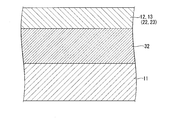
- FIG. 2 is a schematic view of a circuit interface (copper member) and a bonding interface between a metal layer (copper member) and a ceramic substrate (ceramic member) of an insulated circuit board (copper / ceramic joint) according to an embodiment of the present invention.
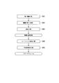
- It is a flowchart which shows the manufacturing method of the insulated circuit board (copper / ceramic bonding body) which is embodiment of this invention.
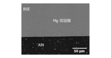
- 5 is an observation result of a bonding interface between a copper plate and a ceramic substrate in the copper / ceramic bonding body of Example 1 of the present invention.
- the copper / ceramic bonding body according to the present embodiment is formed by bonding a ceramic substrate 11 as a ceramic member, a copper plate 22 (circuit layer 12) and a copper plate 23 (metal layer 13) as copper members.
- the insulating circuit board 10 is provided.
- FIG. 1 shows an insulated circuit board 10 according to an embodiment of the present invention and a power module 1 using the insulated circuit board 10.
- the power module 1 includes an insulated circuit board 10, a semiconductor element 3 bonded to one side (upper side in FIG. 1) of the insulated circuit board 10 via a first solder layer 2, and the other side of the insulated circuit board 10. (The lower side in FIG. 1) and a heat sink 51 joined via the second solder layer 8.
- the insulating circuit board 10 includes a ceramic substrate 11, a circuit layer 12 provided on one surface (upper surface in FIG. 1) of the ceramic substrate 11, and a circuit layer 12 provided on the other surface (lower surface in FIG. 1) of the ceramic substrate 11. And a metal layer 13 provided.
- the ceramic substrate 11 prevents electrical connection between the circuit layer 12 and the metal layer 13, and in the present embodiment, is made of highly insulating aluminum nitride.
- the thickness of the ceramic substrate 11 is set in the range of 0.2 mm or more and 1.5 mm or less, and in the present embodiment, the thickness of the ceramic substrate 11 is preferably 0.635 mm.
- the circuit layer 12 is formed by joining a copper plate 22 made of copper or a copper alloy to one surface of the ceramic substrate 11 as shown in FIG.
- a rolled plate of oxygen-free copper is used as the copper plate 22 forming the circuit layer 12.
- a circuit pattern is formed on the circuit layer 12, and one surface thereof (the upper surface in FIG. 1) is a mounting surface on which the semiconductor element 3 is mounted.
- the thickness of the circuit layer 12 is set in the range of 0.1 mm or more and 1.0 mm or less, and in the present embodiment, the thickness of the circuit layer 12 is preferably 0.6 mm.
- the metal layer 13 is formed by joining a copper plate 23 made of copper or a copper alloy to the other surface of the ceramic substrate 11 as shown in FIG.
- a rolled plate of oxygen-free copper is used as the copper plate 23 forming the metal layer 13.
- the thickness of the metal layer 13 is set in the range of 0.1 mm or more and 1.0 mm or less, and in the present embodiment, the thickness of the metal layer 13 is preferably 0.6 mm.
- the heat sink 51 is for cooling the above-mentioned insulated circuit board 10, and in the present embodiment, is a heat radiating plate made of a material having good thermal conductivity. In the present embodiment, the heat sink 51 is preferably made of copper or a copper alloy having excellent thermal conductivity. The heat sink 51 and the metal layer 13 of the insulated circuit board 10 are joined via the second solder layer 8.
- the ceramic substrate 11 and the circuit layer 12 (copper plate 22), and the ceramic substrate 11 and the metal layer 13 (copper plate 23) are joined via an Mg film 25.
- an Mg film 25 At the bonding interface between the ceramic substrate 11 and the circuit layer 12 (copper plate 22) and the bonding interface between the ceramic substrate 11 and the metal layer 13 (copper plate 23), as shown in FIG. A dissolved Mg solid solution layer 32 is formed.
- the Mg content in the Mg solid solution layer 32 is in the range of 0.01 atomic% to 3 atomic%.
- the thickness of the Mg solid solution layer 32 is in the range of 0.1 ⁇ m to 150 ⁇ m, and preferably in the range of 0.1 ⁇ m to 80 ⁇ m.
- the Mg solid solution layer 32 has a concentration gradient such that the Mg concentration gradually increases from the circuit layer 12 (metal layer 13) toward the ceramic substrate 11 side.
- the area ratio of the intermetallic compound phase in a region up to 50 ⁇ m from the joint surface of the ceramic substrate 11 toward the copper plate 22 (circuit layer 12) and copper plate 23 (metal layer 13) is 15% or less. Is preferred. As described above, if the area ratio of the intermetallic compound phase at the bonding interface is suppressed, the Cu-Mg intermetallic compound phase containing Cu and Mg is dispersed inside the Mg solid solution layer 32. Good. Examples of the Cu—Mg intermetallic compound phase include Cu 2 Mg, CuMg 2 and the like.
- Mg placement step S01 As shown in FIG. 4, Mg is disposed between the copper plate 22 serving as the circuit layer 12 and the ceramic substrate 11 and between the copper plate 23 serving as the metal layer 13 and the ceramic substrate 11.
- the Mg film 25 is formed by evaporating Mg.
- the Mg content be placed in a 0.17 mg / cm 2 or more 3.48 mg / cm 2 within the following ranges.
- the pressing load in the joining step S03 is preferably in the range of 0.049 MPa or more and 3.4 MPa or less.
- the heating temperature in the bonding step S03 is preferably in the range of 500 ° C. or more and 850 ° C. or less.
- the degree of vacuum in the bonding step S03 is preferably in the range of 1 ⁇ 10 ⁇ 6 Pa to 5 ⁇ 10 ⁇ 2 Pa.
- the holding time at the heating temperature is preferably in the range of 5 min to 180 min.
- the cooling rate when the temperature is lowered from the heating temperature (bonding temperature) to 480 ° C. is not particularly limited, but is preferably 25 ° C./min or less, more preferably 20 ° C./min or less.
- the lower limit of the temperature decreasing rate is not particularly limited, but may be 3 ° C./min or more, or 5 ° C./min or more.
- the insulated circuit board 10 according to the present embodiment is manufactured by the Mg disposing step S01, the laminating step S02, and the joining step S03.
- Heat sink bonding step S04 Next, a heat sink 51 is joined to the other surface of the metal layer 13 of the insulated circuit board 10.
- the insulated circuit board 10 and the heat sink 51 are stacked via a solder material and charged into a heating furnace, and the insulated circuit board 10 and the heat sink 51 are solder-bonded via the second solder layer 8.
- semiconductor element bonding step S05 Next, the semiconductor element 3 is joined to one surface of the circuit layer 12 of the insulated circuit board 10 by soldering. Through the above steps, the power module 1 shown in FIG. 1 is produced.
- the copper plate 22 (circuit layer 12) and copper plate 23 (metal layer 13) made of oxygen-free copper and aluminum nitride And a ceramic layer 11 are bonded via a Mg film 25, and between the ceramic substrate 11 and the circuit layer 12 (copper plate 22) and between the ceramic substrate 11 and the metal layer 13 (copper plate 22). Since the Mg solid solution layer 32 in which Mg forms a solid solution in the mother phase of Cu is formed, it is disposed between the ceramic substrate 11 and the copper plate 22 (the circuit layer 12) and the copper plate 23 (the metal layer 13).
- Ti, Zr, Nb, and Hf do not exist at the bonding interface between the copper plate 22 (the circuit layer 12) and the copper plate 23 (the metal layer 13) and the ceramic substrate 11, the nitride phase of Ti, Zr, Nb, and Hf and the Ti , Zr, Nb, and Hf are not generated, and cracking of the ceramic substrate 11 can be suppressed even during high-temperature operation.
- the total content of Ti, Zr, Nb, and Hf at the joint interface between the copper plate 22 (the circuit layer 12) and the copper plate 23 (the metal layer 13) and the ceramic substrate 11 is preferably 0.3% by mass or less, and 0.1% by mass. It is more preferred that:
- the Ag content at the bonding interface between the copper plate 22 (the circuit layer 12) and the copper plate 23 (the metal layer 13) and the ceramic substrate 11 is preferably 0.2% by mass or less, and more preferably 0.1% by mass or less. .
- the case where the area ratio of the intermetallic compound phase in the region up to 50 ⁇ m from the joint surface of the ceramic substrate 11 toward the copper plate 22 (circuit layer 12) and copper plate 23 (metal layer 13) is 15% or less. Does not have many hard and brittle intermetallic compound phases in the vicinity of the bonding surface of the ceramic substrate 11, thereby making it possible to reliably suppress cracking of the ceramic substrate 11 during high-temperature operation.
- the area ratio of the intermetallic compound phase in the region up to 50 ⁇ m from the bonding surface of the ceramic substrate 11 toward the copper plate 22 (circuit layer 12) and copper plate 23 (metal layer 13) is preferably 10% or less, and 8% or less. % Is more preferable.
- the amount of Mg is in the range of 0.17 mg / cm 2 or more and 3.48 mg / cm 2 or less, so that a liquid phase necessary for the interfacial reaction can be sufficiently obtained. Therefore, it is possible to obtain the insulated circuit board 10 (copper / ceramic bonded body) in which the copper plates 22 and 23 and the ceramic substrate 11 are securely bonded. Since Ti, Zr, Nb, and Hf are not used for bonding, a nitride phase of Ti, Zr, Nb, and Hf and an intermetallic compound phase containing Ti, Zr, Nb, and Hf are formed near the bonding surface of the ceramic substrate 11.
- an insulated circuit board 10 (copper / ceramic bonded body) that does not exist and can suppress cracking of the ceramic substrate 11 during high-temperature operation. Since Ag is not used for bonding, an insulated circuit board 10 (copper / ceramic bonded body) having excellent migration resistance can be obtained.
- the amount of Mg is in the range of 0.17 mg / cm 2 or more and 3.48 mg / cm 2 or less.
- Mg content lower limit is preferably set to 0.24 mg / cm 2 or more, and even more preferably from 0.32 mg / cm 2 or more.
- the upper limit of the Mg content is preferably set to 2.38 mg / cm 2 or less, and even more preferably from 1.58 mg / cm 2 or less.
- the pressing load in the bonding step S03 is set to 0.049 MPa or more, the ceramic substrate 11, the copper plates 22, 23, and the Mg film 25 can be brought into close contact with each other. Can be promoted. Since the pressing load in the joining step S03 is set to 3.4 MPa or less, cracking of the ceramic substrate 11 in the joining step S03 can be suppressed.
- the lower limit of the pressing load in the joining step S03 is preferably set to 0.098 MPa or more, and more preferably 0.294 MPa or more.
- the upper limit of the pressing load in the joining step S03 is preferably set to 1.96 MPa or less, more preferably 0.98 MPa or less.
- the heating temperature in the bonding step S03 is set to 500 ° C. or higher, which is higher than the eutectic temperature of Cu and Mg, a sufficient liquid phase can be generated at the bonding interface.
- the heating temperature in the bonding step S03 is set to 850 ° C. or less, it is possible to suppress the excessive generation of the liquid phase. Further, the thermal load on the ceramic substrate 11 is reduced, and the deterioration of the ceramic substrate 11 can be suppressed.
- the lower limit of the heating temperature in the bonding step S03 is preferably set to 600 ° C. or higher, more preferably 680 ° C. or higher.
- the upper limit of the heating temperature in the bonding step S03 is preferably set to 800 ° C. or lower, more preferably 760 ° C. or lower.
- the degree of vacuum in the bonding step S03 when the degree of vacuum in the bonding step S03 is in the range of 1 ⁇ 10 ⁇ 6 Pa to 5 ⁇ 10 ⁇ 2 Pa, the oxidation of the Mg film 25 can be suppressed, and the ceramic substrate 11 and the copper plates 22 and 23 can be securely joined.
- the lower limit of the degree of vacuum in the bonding step S03 is preferably 1 ⁇ 10 ⁇ 4 Pa or more, more preferably 1 ⁇ 10 ⁇ 3 Pa or more.
- the upper limit of the degree of vacuum in the bonding step S03 is preferably 1 ⁇ 10 ⁇ 2 Pa or less, more preferably 5 ⁇ 10 ⁇ 3 Pa or less.
- the holding time at the heating temperature in the bonding step S03 when the holding time at the heating temperature in the bonding step S03 is in the range of 5 min to 180 min, the liquid phase can be sufficiently formed, and the ceramic substrate 11 and the copper plates 22 and 23 Can be surely joined.
- the lower limit of the holding time at the heating temperature in the bonding step S03 is preferably 10 min or more, and more preferably 30 min or more.
- the upper limit of the holding time at the heating temperature in the bonding step S03 is preferably 150 min or less, and more preferably 120 min or less.
- the present invention is not limited thereto, and can be appropriately changed without departing from the technical idea of the present invention.
- the copper plate constituting the circuit layer or the metal layer has been described as a rolled plate of oxygen-free copper, the present invention is not limited to this and may be made of another copper or copper alloy.
- the circuit layer and the metal layer are described as being formed of a copper plate.However, the present invention is not limited to this. If at least one of the circuit layer and the metal layer is formed of a copper plate, the other is formed. And other metal plates such as an aluminum plate.
- the Mg film is formed by vapor deposition.
- the Mg film may be formed by another method. It may be arranged. Further, a clad material of Cu and Mg may be arranged.
- a Mg paste and a Cu—Mg paste may be applied. Further, a Cu paste and a Mg paste may be stacked and arranged. At this time, the Mg paste may be disposed on either the copper plate side or the ceramic substrate side. Further, MgH 2 may be arranged as Mg.
- the heat sink has been described as an example of the heat sink, the present invention is not limited to this, and the structure of the heat sink is not particularly limited.
- the heat sink may have a flow path through which a coolant flows, or may include a cooling fin.
- a composite material containing aluminum or an aluminum alloy (for example, AlSiC) can be used as the heat sink.
- a buffer layer made of aluminum, an aluminum alloy, or a composite material containing aluminum (for example, AlSiC) may be provided between the top plate portion of the heat sink or the heat radiating plate and the metal layer.
- the power module is configured by mounting the power semiconductor element on the circuit layer of the insulating circuit board.
- an LED module may be configured by mounting an LED element on an insulated circuit board
- a thermoelectric module may be configured by mounting a thermoelectric element on a circuit layer of the insulated circuit board.
- an active brazing material of Ag-28 mass% Cu-5 mass% Ti was arranged between the ceramic substrate and the copper plate so that the Ag amount was 5.2 mg / cm 2 .
- the cooling rate was controlled to be 5 ° C./min. The cooling rate is controlled by the gas partial pressure during gas cooling (with or without circulation by a cooling fan).
- the bonding interface between the copper plate and the ceramic substrate was measured using an electron beam microanalyzer (JXA-8538F, manufactured by JEOL Ltd.) under the conditions of 2000 times magnification and an acceleration voltage of 15 kV in a region (400 ⁇ m ⁇ 600 ⁇ m) including the bonding interface.
- JXA-8538F electron beam microanalyzer
- the area where the Cu concentration was 5 atom% or more and the Mg concentration was 30 atom or more and 70 atom% or less was obtained by five-point average analysis in the area where the presence of Mg was confirmed.
- the area ratio (%) of the intermetallic compound phase in a region from the joint surface of the ceramic substrate to the copper plate side to 50 ⁇ m was calculated.
- the bonding rate between the copper plate and the ceramic substrate was determined using an ultrasonic flaw detector (FineSAT200 manufactured by Hitachi Power Solutions Co., Ltd.) using the following equation.
- the initial joint area was the area to be joined before joining, that is, the area of the joining surface of the copper plate. Since the peeling is indicated by a white portion in the joined portion in the ultrasonic inspection image, the area of the white portion was defined as the peeling area.
- (Joining rate) ⁇ (initial joining area)-(peeling area) ⁇ / (initial joining area)
- Table 1 shows the evaluation results.
- FIG. 5 shows the results of observation of Example 1 of the present invention.
- Example 1 to 12 of the present invention the initial bonding rate was high, and no cracking of the ceramic substrate was confirmed. The migration was also good. Further, as shown in FIG. 5, as a result of observing the bonding interface, an Mg solid solution layer 32 was observed.
- Examples 21 to 32 of the present invention The copper / ceramic bonded article was prepared in the same manner as the copper / ceramic bonded articles prepared in Examples 1 to 12 of the present invention, and the obtained copper / ceramic bonded article had an area ratio of Cu 2 Mg and ultrasonic bonding.
- the interface was evaluated as follows. The evaluation of the area ratio of the Mg solid solution layer, the Cu-Mg intermetallic compound phase, and the initial bonding rate of the copper / ceramic bonded body were performed in the same manner as the evaluations performed in Examples 1 to 12 of the present invention.
- the area ratio (%) of Cu 2 Mg in the Cu—Mg intermetallic compound phase was defined and calculated by the following formula.
- Cu 2 Mg area ratio (%) Cu 2 Mg area / (Cu 2 Mg area + CuMg 2 area) ⁇ 100
- the “area of Cu 2 Mg” was defined as a region where the Mg concentration was 30 at% or more and less than 60 at%, and the “area of CuMg 2 ” was defined as a region where the Mg concentration was 60 at% or more and less than 70 at%.
- the value of the area ratio of Cu 2 Mg and the bonding property of the ultrasonic bonding changed depending on the temperature drop rate after the bonding step S03. From the results shown in Table 2, it was clarified that the cooling rate was preferably 25 ° C./min or less, more preferably 20 ° C./min or less. From the results shown in Table 2, it became clear that the area ratio of Cu 2 Mg in the Cu-Mg intermetallic compound phase was preferably 55% or more, more preferably 60% or more, and even more preferably 67% or more.
- the copper member and the ceramic member are reliably joined, the migration resistance is excellent, and the occurrence of the ceramic crack at the time of high temperature operation can be suppressed.
- Circuit board can be provided.
- the copper member and the ceramic member are securely bonded by controlling the rate of the temperature drop from the bonding temperature to 480 ° C., and the copper / ceramic bonded body having excellent ultrasonic bonding properties. (Insulated circuit board) can be provided.
Landscapes
- Engineering & Computer Science (AREA)
- Chemical & Material Sciences (AREA)
- Ceramic Engineering (AREA)
- Organic Chemistry (AREA)
- Materials Engineering (AREA)
- Structural Engineering (AREA)
- Manufacturing & Machinery (AREA)
- Mechanical Engineering (AREA)
- Microelectronics & Electronic Packaging (AREA)
- Inorganic Chemistry (AREA)
- Ceramic Products (AREA)
- Manufacturing Of Printed Wiring (AREA)
- Laminated Bodies (AREA)
- Pressure Welding/Diffusion-Bonding (AREA)
Abstract
Description
本願は、2018年8月28日に日本に出願された特願2018-159457号について優先権を主張し、その内容をここに援用する。
例えば、風力発電、電気自動車、ハイブリッド自動車等を制御するために用いられる大電力制御用のパワー半導体素子は、動作時の発熱量が多いことから、これを搭載する基板としては、例えば窒化アルミニウムからなるセラミックス基板と、このセラミックス基板の一方の面に導電性の優れた金属板を接合して形成した回路層と、を備えた絶縁回路基板が、従来から広く用いられている。絶縁回路基板としては、セラミックス基板の他方の面に金属板を接合して金属層を形成したものも提供されている。
さらに、Cu部材とセラミックス部材の接合界面にAgが存在していないので、耐マイグレーション性にも優れている。
この場合、前記セラミックス部材の接合面から前記銅部材側に向けて50μmまでの領域における金属間化合物相の面積率が15%以下とされているので、セラミックス部材の接合面近傍に、硬くて脆い金属間化合物相が多く存在せず、高温動作時のセラミックス部材の割れを確実に抑制することが可能となる。
高温動作時におけるセラミックス基板の割れの発生を抑制することができ、高温条件下においても信頼性高く使用することができる。
この場合、前記セラミックス基板の接合面から前記銅板側に向けて50μmまでの領域における金属間化合物相の面積率が15%以下とされているので、セラミックス基板の接合面近傍に、硬くて脆い金属間化合物相が多く存在せず、高温動作時のセラミックス基板の割れを確実に抑制することが可能となる。
Mg配置工程では、Mg量を0.17mg/cm2以上3.48mg/cm2以下の範囲内としているので、界面反応に必要な液相を十分に得ることができる。よって、銅部材とセラミックス部材とが確実に接合された銅/セラミックス接合体を得ることが可能となる。
接合にTi,Zr,Nb,Hfを用いていないので、セラミックス部材の接合面近傍に、Ti,Zr,Nb,Hfの窒化物相や、Ti,Zr,Nb,Hfを含む金属間化合物相が存在せず、高温動作時におけるセラミックス部材の割れを抑制可能な銅/セラミックス接合体を得ることができる。
接合にAgを用いていないので、耐マイグレーション性に優れた銅/セラミックス接合体を得ることができる。
この場合、前記接合工程における加圧荷重が0.049MPa以上3.4MPa以下の範囲内とされているので、セラミックス部材と銅部材とMgとを密着させることができ、加熱時にこれらの界面反応を促進させることができる。
前記接合工程における加熱温度をCuとMgの共晶温度よりも高い500℃以上としているので、接合界面において十分に液相を生じさせることができる。一方、前記接合工程における加熱温度を850℃以下としているので、液相が過剰に生成することを抑制できる。また、セラミックス部材への熱負荷が小さくなり、セラミックス部材の劣化を抑制することができる。
Mg配置工程では、Mg量を0.17mg/cm2以上3.48mg/cm2以下の範囲内としているので、界面反応に必要な液相を十分に得ることができる。よって、銅板とセラミックス基板とが確実に接合された絶縁回路基板を得ることが可能となる。また、接合にTi,Zr,Nb,Hfを用いていないので、セラミックス基板の接合面近傍に、Ti,Zr,Nb,Hfの窒化物相やTi,Zr,Nb,Hfを含む金属間化合物相が存在せず、高温動作時におけるセラミックス基板の割れを抑制可能な絶縁回路基板を得ることができる。
接合にAgを用いていないので、耐マイグレーション性に優れた絶縁回路基板を得ることができる。
この場合、前記接合工程における加圧荷重が0.049MPa以上3.4MPa以下の範囲内とされているので、セラミックス基板と銅板とMgとを密着させることができ、加熱時にこれらの界面反応を促進させることができる。
前記接合工程における加熱温度をCuとMgの共晶温度よりも高い500℃以上としているので、接合界面において十分に液相を生じさせることができる。一方、前記接合工程における加熱温度を850℃以下としているので、液相が過剰に生成することを抑制できる。また、セラミックス基板への熱負荷が小さくなり、セラミックス基板の劣化を抑制することができる。
図1に、本発明の実施形態である絶縁回路基板10及びこの絶縁回路基板10を用いたパワーモジュール1を示す。
セラミックス基板11は、回路層12と金属層13との間の電気的接続を防止するものであって、本実施形態では、絶縁性の高い窒化アルミニウムで構成されている。セラミックス基板11の厚さは、0.2mm以上1.5mm以下の範囲内に設定されており、本実施形態では、セラミックス基板11の厚さは0.635mmが好ましい。
セラミックス基板11と回路層12(銅板22)との接合界面及びセラミックス基板11と金属層13(銅板23)との接合界面には、図2に示すように、Cuの母相中にMgが固溶したMg固溶層32が形成されている。
このMg固溶層32は、回路層12(金属層13)からセラミックス基板11側に向かうに従い漸次Mg濃度が高くなるような濃度勾配を有している。
上述のように、接合界面における金属間化合物相の面積率が抑制されていれば、Mg固溶層32の内部には、CuとMgを含むCu-Mg金属間化合物相が分散されていてもよい。Cu-Mg金属間化合物相としては、例えばCu2Mg、CuMg2等が挙げられる。
図4に示すように、回路層12となる銅板22とセラミックス基板11との間、及び、金属層13となる銅板23とセラミックス基板11との間に、それぞれMgを配置する。本実施形態では、Mgを蒸着することによって、Mg膜25を形成している。
このMg配置工程S01では、配置するMg量を0.17mg/cm2以上3.48mg/cm2以下の範囲内としている。
次に、銅板22とセラミックス基板11を、Mg膜25を介して積層するとともに、セラミックス基板11と銅板23を、Mg膜25を介して積層する。
次に、積層された銅板22、セラミックス基板11、銅板23を、積層方向に加圧するとともに、真空炉内に装入して加熱し、銅板22とセラミックス基板11と銅板23を接合する。
接合工程S03における加圧荷重は、0.049MPa以上3.4MPa以下の範囲内とすることが好ましい。
接合工程S03における加熱温度は、500℃以上850℃以下の範囲内とすることが好ましい。
接合工程S03における真空度は、1×10⁻⁶Pa以上5×10⁻²Pa以下の範囲内とすることが好ましい。
加熱温度での保持時間は、5min以上180min以下の範囲内とすることが好ましい。
加熱温度(接合温度)から480℃まで降温する際の降温速度は、特に限定されないが、25℃/min以下が好ましく、20℃/min以下がさらに好ましい。また、降温速度の下限値は、特に限定されないが、3℃/min以上としてもよく、5℃/min以上としてもよい。
次に、絶縁回路基板10の金属層13の他方の面側にヒートシンク51を接合する。絶縁回路基板10とヒートシンク51とを、はんだ材を介して積層して加熱炉に装入し、第2はんだ層8を介して絶縁回路基板10とヒートシンク51とをはんだ接合する。
次に、絶縁回路基板10の回路層12の一方の面に、半導体素子3をはんだ付けにより接合する。
以上の工程により、図1に示すパワーモジュール1が製出される。
セラミックス基板11の接合面から銅板22(回路層12)及び銅板23(金属層13)側に向けて50μmまでの領域における金属間化合物相の面積率は、10%以下であることが好ましく、8%以下であることがさらに好ましい。
接合にTi,Zr,Nb,Hfを用いていないので、セラミックス基板11の接合面近傍に、Ti,Zr,Nb,Hfの窒化物相やTi,Zr,Nb,Hfを含む金属間化合物相が存在せず、高温動作時におけるセラミックス基板11の割れを抑制可能な絶縁回路基板10(銅/セラミックス接合体)を得ることができる。
接合にAgを用いていないので、耐マイグレーション性に優れた絶縁回路基板10(銅/セラミックス接合体)を得ることができる。
以上のことから、本実施形態では、Mg量を0.17mg/cm2以上3.48mg/cm2以下の範囲内としている。
Mg量の下限は、0.24mg/cm2以上とすることが好ましく、0.32mg/cm2以上とすることがさらに好ましい。一方、Mg量の上限は、2.38mg/cm2以下とすることが好ましく、1.58mg/cm2以下とすることがさらに好ましい。
接合工程S03における加圧荷重の下限は、0.098MPa以上とすることが好ましく、0.294MPa以上とすることがさらに好ましい。一方、接合工程S03における加圧荷重の上限は、1.96MPa以下とすることが好ましく、0.98MPa以下とすることがさらに好ましい。
接合工程S03における加熱温度の下限は、600℃以上とすることが好ましく、680℃以上とすることがさらに好ましい。一方、接合工程S03における加熱温度の上限は、800℃以下とすることが好ましく、760℃以下とすることがさらに好ましい。
接合工程S03における真空度の下限は、1×10⁻⁴Pa以上とすることが好ましく、1×10⁻³Pa以上とすることがさらに好ましい。一方、接合工程S03における真空度の上限は、1×10⁻²Pa以下とすることが好ましく、5×10⁻³Pa以下とすることがさらに好ましい。
接合工程S03における加熱温度での保持時間の下限は、10min以上とすることが好ましく、30min以上とすることがさらに好ましい。一方、接合工程S03における加熱温度での保持時間の上限は、150min以下とすることが好ましく、120min以下とすることがさらに好ましい。
例えば、回路層又は金属層を構成する銅板を、無酸素銅の圧延板として説明したが、これに限定されることはなく、他の銅又は銅合金で構成されたものであってもよい。
本実施形態においては、回路層及び金属層を銅板で構成したものとして説明したが、これに限定されることはなく、回路層及び金属層の少なくとも一方が銅板で構成されていれば、他方は、アルミニウム板等の他の金属板で構成したものであってもよい。
本実施形態では、Mg配置工程において、Mgペースト及びCu-Mgペーストを塗布してもよい。また、CuペーストとMgペーストを積層して配置してもよい。このとき、Mgペーストは銅板側あるいはセラミックス基板側のいずれに配置してもよい。また、Mgとして、MgH2を配置してもよい。
ヒートシンクの天板部や放熱板と金属層との間に、アルミニウム又はアルミニウム合金若しくはアルミニウムを含む複合材(例えばAlSiC等)からなる緩衝層を設けてもよい。
本発明の有効性を確認するために行った確認実験について説明する。
40mm角の窒化アルミニウムからなるセラミックス基板の両面に、表1に示すようにMgを配置した銅板(無酸素銅、37mm角、厚さ0.15mm)を積層し、表1に示す接合条件で接合し、銅/セラミックス接合体を形成した。セラミックス基板の厚さは厚さ0.635mmとした。また、接合時の真空炉の真空度は5×10-3Paとした。
従来例では、セラミックス基板と銅板の間に、Ag-28mass%Cu-5mass%Tiの活性ろう材を、Ag量が5.2mg/cm2となるように配置した。
また、接合工程S03において、接合温度(表1の「温度(℃)」)から480℃まで降温する際、降温速度は、5℃/minの速度で降温するように制御した。なお、降温速度は、ガス冷却時のガス分圧(冷却ファンによる循環有無)で制御する。
銅板とセラミックス基板との接合界面を、EPMA装置(日本電子株式会社製JXA-8539F)を用いて、倍率2000倍、加速電圧15kVの条件で接合界面を含む領域(400μm×600μm)を観察し、セラミックス基板表面から銅板側に向かって10μm間隔で、銅板の厚さに応じて10点以上20点以下の範囲で定量分析を行い、Mg濃度が0.01原子%以上である領域をMg固溶層とした。
銅板とセラミックス基板との接合界面を、電子線マイクロアナライザー(日本電子株式会社製JXA-8539F)を用いて、倍率2000倍、加速電圧15kVの条件で接合界面を含む領域(400μm×600μm)のMgの元素MAPを取得し、Mgの存在が確認された領域内での定量分析の5点平均で、Cu濃度が5原子%以上、かつ、Mg濃度が30原子以上70原子%以下を満たした領域をCu-Mg金属間化合物相とした。
そして、セラミックス基板の接合面から銅板側に向けて50μmまでの領域における金属間化合物相の面積率(%)を算出した。
銅板とセラミックス基板との接合率は、超音波探傷装置(株式会社日立パワーソリューションズ製FineSAT200)を用いて以下の式を用いて求めた。初期接合面積とは、接合前における接合すべき面積、すなわち銅板の接合面の面積とした。超音波探傷像において剥離は接合部内の白色部で示されることから、この白色部の面積を剥離面積とした。
(接合率)={(初期接合面積)-(剥離面積)}/(初期接合面積)
冷熱衝撃試験機(エスペック株式会社製TSA-72ES)を使用し、気相で、-50℃×10分←→150℃×10分の300サイクルを実施した。
上述の冷熱サイクルを負荷した後のセラミックス基板の割れの有無を評価した。
回路層において絶縁分離された回路パターン間距離0.5mm、温度85℃、湿度85%RH、電圧DC50Vの条件で、2000時間放置後に、回路パターン間の電気抵抗を測定し、抵抗値が1×10⁶Ω以下となった場合を短絡した(マイグレーションが発生した)と判断し、マイグレーションの評価を「B」とした。上記と同じ条件で、2000時間放置後に、回路パターン間の電気抵抗を測定し、抵抗値が1×10⁶Ωより大きい場合は、マイグレーションが発生しなかったと判断し、マイグレーションの評価を「A」とした。

Mg配置工程において、Mg量が4.75mg/cm2と本発明の範囲よりも多い比較例2においては、接合時に液相が過剰に生成したため、液相が接合界面から漏れ出し、所定の形状の接合体を製造できなかった。このため、その後の評価を中止した。
また、図5に示すように、接合界面を観察した結果、Mg固溶層32が観察された。
銅/セラミックス接合体は、上記本発明例1~12で作製した銅/セラミックス接合体と同様に作製し、得られた銅/セラミックス接合体について、Cu2Mgの面積率、および、超音波接合界面を、以下のように評価した。
Mg固溶層、Cu-Mg金属間化合物相の面積率、および、銅/セラミックス接合体の初期接合率の評価は、上記本発明例1~12で行った評価と同様に行った。
接合工程S03において、接合温度(表2の「温度(℃)」)から480℃まで降温する際、降温速度は、表2に示す速度で制御した。
上記Cu-Mg金属間化合物相のうち、Cu2Mgの面積率(%)を以下の計算式で定義し、算出した。
Cu2Mgの面積率(%)=Cu2Mgの面積/(Cu2Mgの面積+CuMg2の面積)×100
「Cu2Mgの面積」は、Mg濃度が30at%以上60at%未満の領域とし、「CuMg2の面積」は、Mg濃度が60at%以上70at%未満の領域とした。
得られた銅/セラミックス接合体に対して、超音波金属接合機(超音波工業株式会社製:60C-904)を用いて、銅端子(10mm×5mm×1.5mm厚)をコプラス量0.5mmの条件で超音波接合した。
接合後に、超音波探傷装置(株式会社日立ソリューションズ製FineSAT200)を用いて、銅板とセラミックス基板の接合界面を検査し、セラミックス割れが観察されたものを「C」、剥離が観察されたものを「B」、どちらも確認されなかったものを「A」と評価した。評価結果を表2に示す。
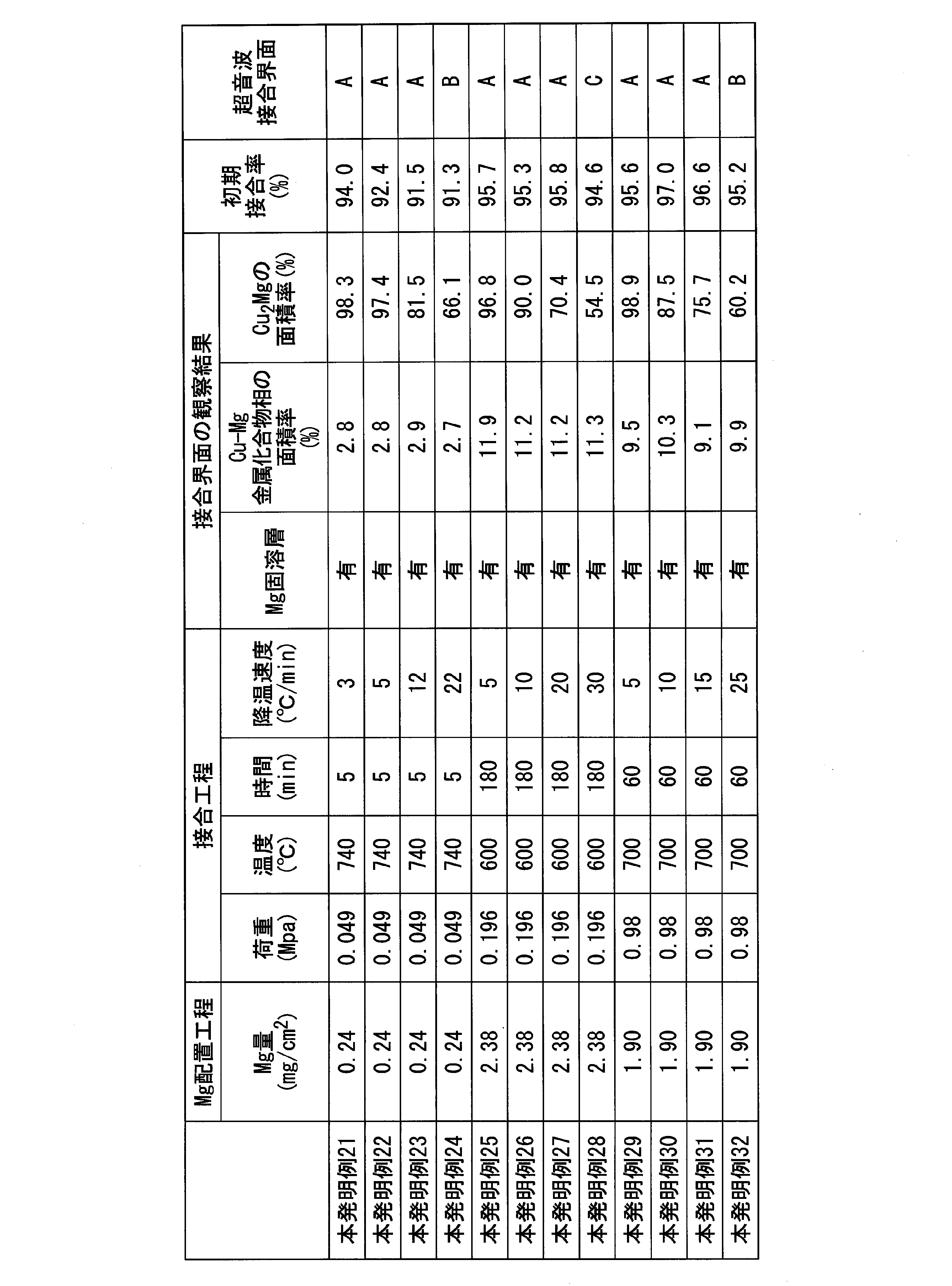
表2に示す結果から、降温速度は、25℃/min以下が好ましく、20℃/min以下がさらに好ましいことが明らかとなった。
表2に示す結果から、Cu-Mg金属間化合物相のうち、Cu2Mgの面積率は55%以上が好ましく、60%以上がより好ましく、67%以上が更に好ましいことが明らかとなった。
11 セラミックス基板
12 回路層
13 金属層
22、23 銅板
32 Mg固溶層
Claims (8)
- 銅又は銅合金からなる銅部材と、窒化アルミニウムからなるセラミックス部材とが接合されてなる銅/セラミックス接合体であって、
前記銅部材と前記セラミックス部材との間に、Cuの母相中にMgが固溶したMg固溶層が形成されていることを特徴とする銅/セラミックス接合体。 - 前記セラミックス部材の接合面から前記銅部材側に向けて50μmまでの領域における金属間化合物相の面積率が15%以下であることを特徴とする請求項1に記載の銅/セラミックス接合体。
- 窒化アルミニウムからなるセラミックス基板の表面に、銅又は銅合金からなる銅板が接合されてなる絶縁回路基板であって、
前記銅板と前記セラミックス基板との間に、Cuの母相中にMgが固溶したMg固溶層が形成されていることを特徴とする絶縁回路基板。 - 前記セラミックス基板の接合面から前記銅板側に向けて50μmまでの領域における金属間化合物相の面積率が15%以下であることを特徴とする請求項3に記載の絶縁回路基板。
- 請求項1又は請求項2に記載の銅/セラミックス接合体を製造する銅/セラミックス接合体の製造方法であって、
前記銅部材と前記セラミックス部材との間に、Mgを配置するMg配置工程と、
前記銅部材と前記セラミックス部材とをMgを介して積層する積層工程と、
Mgを介して積層された前記銅部材と前記セラミックス部材とを積層方向に加圧した状態で、真空雰囲気下において加熱処理して接合する接合工程と、
を備えており、
前記Mg配置工程では、Mg量を0.17mg/cm2以上3.48mg/cm2以下の範囲内とすることを特徴とする銅/セラミックス接合体の製造方法。 - 前記接合工程における加圧荷重が0.049MPa以上3.4MPa以下の範囲内とされ、加熱温度が500℃以上850℃以下の範囲内とされていることを特徴とする請求項5に記載の銅/セラミックス接合体の製造方法。
- 請求項3又は請求項4に記載の絶縁回路基板の製造方法であって、
前記銅板と前記セラミックス基板との間に、Mgを配置するMg配置工程と、
前記銅板と前記セラミックス基板とをMgを介して積層する積層工程と、
Mgを介して積層された前記銅板と前記セラミックス基板とを積層方向に加圧した状態で、真空雰囲気下において加熱処理して接合する接合工程と、
を備えており、
前記Mg配置工程では、Mg量を0.17mg/cm2以上3.48mg/cm2以下の範囲内とすることを特徴とする絶縁回路基板の製造方法。 - 前記接合工程における加圧荷重が0.049MPa以上3.4MPa以下の範囲内とされ、加熱温度が500℃以上850℃以下の範囲内とされていることを特徴とする請求項7に記載の絶縁回路基板の製造方法。
Priority Applications (5)
| Application Number | Priority Date | Filing Date | Title |
|---|---|---|---|
| CN201980056156.2A CN112654593B (zh) | 2018-08-28 | 2019-08-27 | 铜-陶瓷接合体、绝缘电路基板、铜-陶瓷接合体的制造方法及绝缘电路基板的制造方法 |
| JP2020539478A JP7008188B2 (ja) | 2018-08-28 | 2019-08-27 | 銅/セラミックス接合体、絶縁回路基板、及び、銅/セラミックス接合体の製造方法、及び、絶縁回路基板の製造方法 |
| US17/270,149 US12168634B2 (en) | 2018-08-28 | 2019-08-27 | Copper/ceramic bonded body, insulating circuit substrate, copper/ceramic bonded body production method, and insulating circuit substrate production method |
| KR1020217004791A KR102409815B1 (ko) | 2018-08-28 | 2019-08-27 | 구리/세라믹스 접합체, 절연 회로 기판, 및 구리/세라믹스 접합체의 제조 방법, 및 절연 회로 기판의 제조 방법 |
| EP19854442.1A EP3845511B1 (en) | 2018-08-28 | 2019-08-27 | Copper/ceramic bonded body, insulating circuit board, method for producing copper/ceramic bonded body, and method for manufacturing insulating circuit board |
Applications Claiming Priority (2)
| Application Number | Priority Date | Filing Date | Title |
|---|---|---|---|
| JP2018159457 | 2018-08-28 | ||
| JP2018-159457 | 2018-08-28 |
Publications (1)
| Publication Number | Publication Date |
|---|---|
| WO2020045403A1 true WO2020045403A1 (ja) | 2020-03-05 |
Family
ID=69645068
Family Applications (2)
| Application Number | Title | Priority Date | Filing Date |
|---|---|---|---|
| PCT/JP2019/004022 Ceased WO2020044594A1 (ja) | 2018-08-28 | 2019-02-05 | 銅/セラミックス接合体、絶縁回路基板、及び、銅/セラミックス接合体の製造方法、及び、絶縁回路基板の製造方法 |
| PCT/JP2019/033461 Ceased WO2020045403A1 (ja) | 2018-08-28 | 2019-08-27 | 銅/セラミックス接合体、絶縁回路基板、及び、銅/セラミックス接合体の製造方法、及び、絶縁回路基板の製造方法 |
Family Applications Before (1)
| Application Number | Title | Priority Date | Filing Date |
|---|---|---|---|
| PCT/JP2019/004022 Ceased WO2020044594A1 (ja) | 2018-08-28 | 2019-02-05 | 銅/セラミックス接合体、絶縁回路基板、及び、銅/セラミックス接合体の製造方法、及び、絶縁回路基板の製造方法 |
Country Status (7)
| Country | Link |
|---|---|
| US (1) | US12168634B2 (ja) |
| EP (1) | EP3845511B1 (ja) |
| JP (1) | JP7008188B2 (ja) |
| KR (1) | KR102409815B1 (ja) |
| CN (1) | CN112654593B (ja) |
| TW (2) | TW202017118A (ja) |
| WO (2) | WO2020044594A1 (ja) |
Families Citing this family (3)
| Publication number | Priority date | Publication date | Assignee | Title |
|---|---|---|---|---|
| TWI751797B (zh) * | 2020-11-19 | 2022-01-01 | 頎邦科技股份有限公司 | 電路板及其散熱貼片 |
| JP7694291B2 (ja) * | 2021-09-21 | 2025-06-18 | 三菱マテリアル株式会社 | 銅/セラミックス接合体、および、絶縁回路基板 |
| JP7647471B2 (ja) * | 2021-09-21 | 2025-03-18 | 三菱マテリアル株式会社 | 銅/セラミックス接合体、および、絶縁回路基板 |
Citations (8)
| Publication number | Priority date | Publication date | Assignee | Title |
|---|---|---|---|---|
| JPH04162756A (ja) | 1990-10-26 | 1992-06-08 | Toshiba Corp | 半導体モジュール |
| JPH08277171A (ja) * | 1995-02-09 | 1996-10-22 | Ngk Insulators Ltd | 接合体、耐蝕性接合材料および接合体の製造方法 |
| JPH08277173A (ja) * | 1995-02-09 | 1996-10-22 | Ngk Insulators Ltd | セラミックスの接合構造およびその製造方法 |
| JP3211856B2 (ja) | 1994-11-02 | 2001-09-25 | 電気化学工業株式会社 | 回路基板 |
| JP2005305526A (ja) * | 2004-04-23 | 2005-11-04 | Honda Motor Co Ltd | 銅とセラミックス又は炭素基銅複合材料との接合用ろう材及び同接合方法 |
| WO2015141839A1 (ja) * | 2014-03-20 | 2015-09-24 | Jx日鉱日石金属株式会社 | 積層体及び、その製造方法 |
| JP2018140929A (ja) * | 2017-02-28 | 2018-09-13 | 三菱マテリアル株式会社 | 銅/セラミックス接合体、絶縁回路基板、及び、銅/セラミックス接合体の製造方法、絶縁回路基板の製造方法 |
| JP2018159457A (ja) | 2017-03-23 | 2018-10-11 | 未来工業株式会社 | 排気弁装置及び弁体設置装置 |
Family Cites Families (34)
| Publication number | Priority date | Publication date | Assignee | Title |
|---|---|---|---|---|
| JP3302714B2 (ja) * | 1992-01-27 | 2002-07-15 | 株式会社東芝 | セラミックス−金属接合体 |
| JPH0726239A (ja) * | 1993-07-13 | 1995-01-27 | Sekisui Chem Co Ltd | 合成樹脂ライニング管用接着剤組成物 |
| JP3260222B2 (ja) * | 1993-11-24 | 2002-02-25 | 電気化学工業株式会社 | 回路基板の製造方法 |
| AT405039B (de) * | 1996-02-08 | 1999-04-26 | Electrovac | Verbundbauteil |
| JP3342797B2 (ja) * | 1996-03-01 | 2002-11-11 | 電気化学工業株式会社 | 金属回路を有するセラミックス回路基板の製造方法 |
| JP3288922B2 (ja) * | 1996-03-14 | 2002-06-04 | 日本碍子株式会社 | 接合体およびその製造方法 |
| DE60037069T2 (de) * | 1999-05-28 | 2008-09-11 | Denki Kagaku Kogyo K.K. | Schaltung mit Substrat |
| JP2001160676A (ja) * | 1999-12-01 | 2001-06-12 | Denki Kagaku Kogyo Kk | セラミックス回路基板 |
| JP4627839B2 (ja) * | 2000-05-01 | 2011-02-09 | 電気化学工業株式会社 | モジュールとその製造方法 |
| US7019975B2 (en) * | 2000-08-09 | 2006-03-28 | Mitsubishi Materials Corporation | Power module and power module with heat sink |
| US7069645B2 (en) * | 2001-03-29 | 2006-07-04 | Ngk Insulators, Ltd. | Method for producing a circuit board |
| EP1498946B1 (en) * | 2002-04-19 | 2012-04-04 | Mitsubishi Materials Corporation | Circuit board, process for producing the same and power module |
| JP2004231452A (ja) * | 2003-01-29 | 2004-08-19 | Honda Motor Co Ltd | 炭素基金属複合材とセラミックスとの接合方法 |
| JP4108505B2 (ja) | 2003-02-26 | 2008-06-25 | 本田技研工業株式会社 | 炭素基銅複合材とセラミックス又は銅との接合方法 |
| DE112004001032T5 (de) * | 2003-06-13 | 2006-05-18 | Han, Joo-Hwan, Kyungsan | Verfahren zum Verbinden von Keramik: Reaktions-Diffusionsbinden |
| EP1926142A1 (en) * | 2005-09-15 | 2008-05-28 | Mitsubishi Materials Corporation | Insulating circuit board and insulating circuit board provided with cooling sink section |
| EP2002915B1 (en) * | 2006-03-15 | 2011-10-12 | NGK Insulators, Ltd. | Method of fabricating dissimilar material jointed body |
| JP4717960B2 (ja) * | 2009-04-03 | 2011-07-06 | 株式会社住友金属エレクトロデバイス | セラミックス焼結体およびそれを用いた半導体装置用基板 |
| CN104011852B (zh) * | 2011-12-20 | 2016-12-21 | 株式会社东芝 | 陶瓷铜电路基板和使用了陶瓷铜电路基板的半导体装置 |
| EP2811513B1 (en) * | 2012-02-01 | 2019-12-18 | Mitsubishi Materials Corporation | Method for producing substrate for power modules |
| US10105795B2 (en) * | 2012-05-25 | 2018-10-23 | General Electric Company | Braze compositions, and related devices |
| JP6056432B2 (ja) * | 2012-12-06 | 2017-01-11 | 三菱マテリアル株式会社 | パワーモジュール用基板、ヒートシンク付パワーモジュール用基板、パワーモジュール、パワーモジュール用基板の製造方法 |
| JP5672324B2 (ja) * | 2013-03-18 | 2015-02-18 | 三菱マテリアル株式会社 | 接合体の製造方法及びパワーモジュール用基板の製造方法 |
| EP3041045B1 (en) * | 2013-08-26 | 2019-09-18 | Mitsubishi Materials Corporation | Bonded body and power module substrate |
| EP3053899B1 (en) * | 2013-09-30 | 2019-11-06 | Mitsubishi Materials Corporation | Cu/ceramic bonded body, method for manufacturing cu/ceramic bonded body, and power module substrate |
| KR101758586B1 (ko) | 2014-02-12 | 2017-07-14 | 미쓰비시 마테리알 가부시키가이샤 | 구리/세라믹스 접합체 및 파워 모듈용 기판 |
| JP6256176B2 (ja) * | 2014-04-25 | 2018-01-10 | 三菱マテリアル株式会社 | 接合体の製造方法、パワーモジュール用基板の製造方法 |
| JP6638282B2 (ja) * | 2015-09-25 | 2020-01-29 | 三菱マテリアル株式会社 | 冷却器付き発光モジュールおよび冷却器付き発光モジュールの製造方法 |
| JP6656657B2 (ja) * | 2015-11-06 | 2020-03-04 | 三菱マテリアル株式会社 | セラミックス/アルミニウム接合体、パワーモジュール用基板、及び、パワーモジュール |
| JP6729224B2 (ja) | 2015-11-26 | 2020-07-22 | 三菱マテリアル株式会社 | セラミックス/アルミニウム接合体、絶縁回路基板、パワーモジュール、ledモジュール、熱電モジュール |
| JP2017135374A (ja) * | 2016-01-22 | 2017-08-03 | 三菱マテリアル株式会社 | 接合体、パワーモジュール用基板、パワーモジュール、接合体の製造方法及びパワーモジュール用基板の製造方法 |
| JP6572810B2 (ja) * | 2016-03-15 | 2019-09-11 | 三菱マテリアル株式会社 | 接合体の製造方法、及び、パワーモジュール用基板の製造方法 |
| WO2018159590A1 (ja) * | 2017-02-28 | 2018-09-07 | 三菱マテリアル株式会社 | 銅/セラミックス接合体、絶縁回路基板、及び、銅/セラミックス接合体の製造方法、絶縁回路基板の製造方法 |
| JP3211856U (ja) | 2017-05-09 | 2017-08-10 | 株式会社アイエスピー | メジャー付きタオル |
-
2019
- 2019-02-05 WO PCT/JP2019/004022 patent/WO2020044594A1/ja not_active Ceased
- 2019-02-14 TW TW108104894A patent/TW202017118A/zh unknown
- 2019-08-26 TW TW108130412A patent/TWI801652B/zh not_active IP Right Cessation
- 2019-08-27 US US17/270,149 patent/US12168634B2/en active Active
- 2019-08-27 JP JP2020539478A patent/JP7008188B2/ja active Active
- 2019-08-27 KR KR1020217004791A patent/KR102409815B1/ko not_active Expired - Fee Related
- 2019-08-27 WO PCT/JP2019/033461 patent/WO2020045403A1/ja not_active Ceased
- 2019-08-27 CN CN201980056156.2A patent/CN112654593B/zh active Active
- 2019-08-27 EP EP19854442.1A patent/EP3845511B1/en active Active
Patent Citations (9)
| Publication number | Priority date | Publication date | Assignee | Title |
|---|---|---|---|---|
| JPH04162756A (ja) | 1990-10-26 | 1992-06-08 | Toshiba Corp | 半導体モジュール |
| JP3211856B2 (ja) | 1994-11-02 | 2001-09-25 | 電気化学工業株式会社 | 回路基板 |
| JPH08277171A (ja) * | 1995-02-09 | 1996-10-22 | Ngk Insulators Ltd | 接合体、耐蝕性接合材料および接合体の製造方法 |
| JPH08277173A (ja) * | 1995-02-09 | 1996-10-22 | Ngk Insulators Ltd | セラミックスの接合構造およびその製造方法 |
| JP2005305526A (ja) * | 2004-04-23 | 2005-11-04 | Honda Motor Co Ltd | 銅とセラミックス又は炭素基銅複合材料との接合用ろう材及び同接合方法 |
| JP4375730B2 (ja) | 2004-04-23 | 2009-12-02 | 本田技研工業株式会社 | 銅とセラミックス又は炭素基銅複合材料との接合用ろう材及び同接合方法 |
| WO2015141839A1 (ja) * | 2014-03-20 | 2015-09-24 | Jx日鉱日石金属株式会社 | 積層体及び、その製造方法 |
| JP2018140929A (ja) * | 2017-02-28 | 2018-09-13 | 三菱マテリアル株式会社 | 銅/セラミックス接合体、絶縁回路基板、及び、銅/セラミックス接合体の製造方法、絶縁回路基板の製造方法 |
| JP2018159457A (ja) | 2017-03-23 | 2018-10-11 | 未来工業株式会社 | 排気弁装置及び弁体設置装置 |
Non-Patent Citations (1)
| Title |
|---|
| See also references of EP3845511A4 |
Also Published As
| Publication number | Publication date |
|---|---|
| KR20210043586A (ko) | 2021-04-21 |
| KR102409815B1 (ko) | 2022-06-15 |
| TW202017118A (zh) | 2020-05-01 |
| CN112654593A (zh) | 2021-04-13 |
| EP3845511B1 (en) | 2026-01-14 |
| JPWO2020045403A1 (ja) | 2021-08-12 |
| US12168634B2 (en) | 2024-12-17 |
| EP3845511A1 (en) | 2021-07-07 |
| TW202021055A (zh) | 2020-06-01 |
| JP7008188B2 (ja) | 2022-01-25 |
| CN112654593B (zh) | 2022-11-11 |
| US20210238103A1 (en) | 2021-08-05 |
| TWI801652B (zh) | 2023-05-11 |
| EP3845511A4 (en) | 2022-04-27 |
| WO2020044594A1 (ja) | 2020-03-05 |
Similar Documents
| Publication | Publication Date | Title |
|---|---|---|
| KR102459745B1 (ko) | 구리/세라믹스 접합체, 절연 회로 기판, 및, 구리/세라믹스 접합체의 제조 방법, 절연 회로 기판의 제조 방법 | |
| JP7056744B2 (ja) | 銅/セラミックス接合体、絶縁回路基板、及び、銅/セラミックス接合体の製造方法、及び、絶縁回路基板の製造方法 | |
| JP7136212B2 (ja) | 銅/セラミックス接合体、絶縁回路基板、及び、銅/セラミックス接合体の製造方法、及び、絶縁回路基板の製造方法 | |
| JP7192451B2 (ja) | 銅/セラミックス接合体、絶縁回路基板、及び、銅/セラミックス接合体の製造方法、絶縁回路基板の製造方法 | |
| WO2018159590A1 (ja) | 銅/セラミックス接合体、絶縁回路基板、及び、銅/セラミックス接合体の製造方法、絶縁回路基板の製造方法 | |
| WO2021033421A1 (ja) | 銅/セラミックス接合体、絶縁回路基板、及び、銅/セラミックス接合体の製造方法、絶縁回路基板の製造方法 | |
| JP7008188B2 (ja) | 銅/セラミックス接合体、絶縁回路基板、及び、銅/セラミックス接合体の製造方法、及び、絶縁回路基板の製造方法 | |
| JP7794558B2 (ja) | 銅/セラミックス接合体、絶縁回路基板、及び、銅/セラミックス接合体の製造方法、絶縁回路基板の製造方法 | |
| JP7424043B2 (ja) | 銅/セラミックス接合体、絶縁回路基板、及び、銅/セラミックス接合体の製造方法、絶縁回路基板の製造方法 | |
| JP7512863B2 (ja) | 銅/セラミックス接合体、絶縁回路基板、及び、銅/セラミックス接合体の製造方法、絶縁回路基板の製造方法 | |
| CN114127921B (zh) | 铜-陶瓷接合体、绝缘电路基板、铜-陶瓷接合体的制造方法及绝缘电路基板的制造方法 | |
| WO2021112046A1 (ja) | 銅/セラミックス接合体、絶縁回路基板、及び、銅/セラミックス接合体の製造方法、絶縁回路基板の製造方法 | |
| JP2021031315A (ja) | 銅/セラミックス接合体、絶縁回路基板、及び、銅/セラミックス接合体の製造方法、絶縁回路基板の製造方法 | |
| JP6850984B2 (ja) | 銅/セラミックス接合体、絶縁回路基板、及び、銅/セラミックス接合体の製造方法、絶縁回路基板の製造方法 | |
| CN117222608A (zh) | 铜-陶瓷接合体及绝缘电路基板 |
Legal Events
| Date | Code | Title | Description |
|---|---|---|---|
| 121 | Ep: the epo has been informed by wipo that ep was designated in this application |
Ref document number: 19854442 Country of ref document: EP Kind code of ref document: A1 |
|
| ENP | Entry into the national phase |
Ref document number: 2020539478 Country of ref document: JP Kind code of ref document: A |
|
| ENP | Entry into the national phase |
Ref document number: 20217004791 Country of ref document: KR Kind code of ref document: A |
|
| NENP | Non-entry into the national phase |
Ref country code: DE |
|
| ENP | Entry into the national phase |
Ref document number: 2019854442 Country of ref document: EP Effective date: 20210329 |
|
| WWG | Wipo information: grant in national office |
Ref document number: 2019854442 Country of ref document: EP |