WO2020054629A1 - 固体撮像素子及び電子機器 - Google Patents
固体撮像素子及び電子機器 Download PDFInfo
- Publication number
- WO2020054629A1 WO2020054629A1 PCT/JP2019/035240 JP2019035240W WO2020054629A1 WO 2020054629 A1 WO2020054629 A1 WO 2020054629A1 JP 2019035240 W JP2019035240 W JP 2019035240W WO 2020054629 A1 WO2020054629 A1 WO 2020054629A1
- Authority
- WO
- WIPO (PCT)
- Prior art keywords
- signal
- pixel
- comparator
- channel mos
- noise
- Prior art date
- Legal status (The legal status is an assumption and is not a legal conclusion. Google has not performed a legal analysis and makes no representation as to the accuracy of the status listed.)
- Ceased
Links
Images



Classifications
-
- H—ELECTRICITY
- H04—ELECTRIC COMMUNICATION TECHNIQUE
- H04N—PICTORIAL COMMUNICATION, e.g. TELEVISION
- H04N25/00—Circuitry of solid-state image sensors [SSIS]; Control thereof
- H04N25/70—SSIS architectures; Circuits associated therewith
- H04N25/71—Charge-coupled device [CCD] sensors; Charge-transfer registers specially adapted for CCD sensors
- H04N25/75—Circuitry for providing, modifying or processing image signals from the pixel array
-
- H—ELECTRICITY
- H04—ELECTRIC COMMUNICATION TECHNIQUE
- H04N—PICTORIAL COMMUNICATION, e.g. TELEVISION
- H04N25/00—Circuitry of solid-state image sensors [SSIS]; Control thereof
- H04N25/60—Noise processing, e.g. detecting, correcting, reducing or removing noise
-
- H—ELECTRICITY
- H04—ELECTRIC COMMUNICATION TECHNIQUE
- H04N—PICTORIAL COMMUNICATION, e.g. TELEVISION
- H04N25/00—Circuitry of solid-state image sensors [SSIS]; Control thereof
- H04N25/60—Noise processing, e.g. detecting, correcting, reducing or removing noise
- H04N25/617—Noise processing, e.g. detecting, correcting, reducing or removing noise for reducing electromagnetic interference, e.g. clocking noise
-
- H—ELECTRICITY
- H03—ELECTRONIC CIRCUITRY
- H03K—PULSE TECHNIQUE
- H03K5/00—Manipulating of pulses not covered by one of the other main groups of this subclass
- H03K5/01—Shaping pulses
- H03K5/08—Shaping pulses by limiting; by thresholding; by slicing, i.e. combined limiting and thresholding
-
- H—ELECTRICITY
- H03—ELECTRONIC CIRCUITRY
- H03K—PULSE TECHNIQUE
- H03K5/00—Manipulating of pulses not covered by one of the other main groups of this subclass
- H03K5/22—Circuits having more than one input and one output for comparing pulses or pulse trains with each other according to input signal characteristics, e.g. slope, integral
- H03K5/24—Circuits having more than one input and one output for comparing pulses or pulse trains with each other according to input signal characteristics, e.g. slope, integral the characteristic being amplitude
- H03K5/2472—Circuits having more than one input and one output for comparing pulses or pulse trains with each other according to input signal characteristics, e.g. slope, integral the characteristic being amplitude using field effect transistors
- H03K5/2481—Circuits having more than one input and one output for comparing pulses or pulse trains with each other according to input signal characteristics, e.g. slope, integral the characteristic being amplitude using field effect transistors with at least one differential stage
-
- H—ELECTRICITY
- H03—ELECTRONIC CIRCUITRY
- H03M—CODING; DECODING; CODE CONVERSION IN GENERAL
- H03M1/00—Analogue/digital conversion; Digital/analogue conversion
- H03M1/06—Continuously compensating for, or preventing, undesired influence of physical parameters
- H03M1/08—Continuously compensating for, or preventing, undesired influence of physical parameters of noise
-
- H—ELECTRICITY
- H03—ELECTRONIC CIRCUITRY
- H03M—CODING; DECODING; CODE CONVERSION IN GENERAL
- H03M1/00—Analogue/digital conversion; Digital/analogue conversion
- H03M1/06—Continuously compensating for, or preventing, undesired influence of physical parameters
- H03M1/08—Continuously compensating for, or preventing, undesired influence of physical parameters of noise
- H03M1/0845—Continuously compensating for, or preventing, undesired influence of physical parameters of noise of power supply variations, e.g. ripple
-
- H—ELECTRICITY
- H03—ELECTRONIC CIRCUITRY
- H03M—CODING; DECODING; CODE CONVERSION IN GENERAL
- H03M1/00—Analogue/digital conversion; Digital/analogue conversion
- H03M1/12—Analogue/digital converters
- H03M1/1205—Multiplexed conversion systems
- H03M1/123—Simultaneous, i.e. using one converter per channel but with common control or reference circuits for multiple converters
-
- H—ELECTRICITY
- H04—ELECTRIC COMMUNICATION TECHNIQUE
- H04N—PICTORIAL COMMUNICATION, e.g. TELEVISION
- H04N25/00—Circuitry of solid-state image sensors [SSIS]; Control thereof
- H04N25/70—SSIS architectures; Circuits associated therewith
- H04N25/76—Addressed sensors, e.g. MOS or CMOS sensors
- H04N25/78—Readout circuits for addressed sensors, e.g. output amplifiers or A/D converters
-
- H—ELECTRICITY
- H03—ELECTRONIC CIRCUITRY
- H03M—CODING; DECODING; CODE CONVERSION IN GENERAL
- H03M1/00—Analogue/digital conversion; Digital/analogue conversion
- H03M1/12—Analogue/digital converters
- H03M1/50—Analogue/digital converters with intermediate conversion to time interval
- H03M1/56—Input signal compared with linear ramp
Definitions
- the present disclosure relates to a solid-state imaging device and an electronic device.
- CMOS Complementary Metal Oxide Semiconductor
- the noise of the pixel power supply is captured, converted into a current having appropriate gain and frequency characteristics, and the current is supplied to an output resistor of a D / A converter for generating a ramp wave to generate a voltage.
- a configuration is adopted in which the differential pair of the comparator cancels out.
- An object of the present disclosure is to provide a solid-state imaging device and an electronic device that can remove pixel power supply noise, reduce a conversion error, and suppress a decrease in image quality even when an ultra-low voltage comparator is used as a comparator.
- the solid-state imaging device of the present disclosure is connected to a pixel and a pixel power supply that supplies power to the pixel, and generates a first noise cancellation signal for canceling power supply noise of the pixel power supply.
- a noise cancellation signal generation circuit that performs gain switching and polarity inversion based on a gain control signal with respect to the first noise cancellation signal and outputs the same as a second noise cancellation signal, and generates and outputs a reference signal that is a ramp signal.
- a DA converter that converts the current of the noise cancel signal into a voltage and superimposes it on the ramp signal, and a reference signal and a pixel signal are input to the comparator body via an input capacitor connected to one terminal of the differential pair, and the pixel signal And a comparator that outputs an inverted signal having a timing according to the gain setting and the inverted timing of the comparator.
- the noise cancellation signal generation circuit generates the first noise cancellation signal for canceling the power supply noise of the pixel power supply, and performs gain switching and polarity inversion based on the gain control signal with respect to the first noise cancellation signal. And outputs it to the DA converter as a second noise cancellation signal.
- the D / A converter generates a reference signal, which is a ramp signal, by flowing a current output from a variable current source controlled by a digital value into an output resistor, and outputs the reference signal to a comparator.
- the second noise cancellation signal is output to the DA converter as a current, is converted into a voltage by flowing into the output resistance of the DA converter, is superimposed on the ramp signal, and is output to the comparator.
- the comparator inputs the reference signal and the pixel signal to the comparator main body via an input capacitor connected to one terminal of the differential pair, and outputs an inverted signal having a timing according to the pixel signal and the gain setting to the counter.
- the counter converts the inversion timing of the comparator into a digital value and outputs the digital value.
- the gain control unit outputs a gain control signal based on the change amount of the input capacitance to the noise cancellation signal generation circuit when performing the gain control of the comparator by changing the slope of the reference signal and the input capacitance.
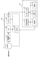
- FIG. 1 is a schematic configuration diagram illustrating an example of a solid-state imaging device according to an embodiment.
- FIG. 4 is an explanatory diagram of a circuit configuration example of an ULV comparator.
- FIG. 9 is an explanatory diagram of a configuration example of a PSRR correction circuit.
- FIG. 4 is an explanatory diagram showing a relationship between a gain of a single slope AD converter and an amplitude of a ramp signal.
- FIG. 4 is a diagram illustrating the relationship between the input capacitance on the ramp signal side, the input capacitance on the pixel signal side, and the gain of the single slope AD converter. It is explanatory drawing of an example of the floor plan of an image sensor.
- FIG. 11 is a diagram illustrating a configuration example of an imaging device as another electronic device.
- FIG. 11 is a diagram illustrating a configuration example of an imaging device as still another electronic device.
- FIG. 1 is a schematic configuration diagram illustrating an example of the solid-state imaging device according to the embodiment.
- Examples of the solid-state imaging device according to the embodiment include a CCD image sensor and a CMOS image sensor.
- the solid-state imaging device 10 includes a pixel 11, a PSRR correction circuit 12, a DA converter 13, an ultra-low voltage (ULV) comparator 14, a gain control unit 15, and a load MOS transistor 16.
- a plurality of pixels (for example, N rows ⁇ M columns, where N and M are integers of 2 or more) are provided in the solid-state imaging device 10 connected to the power supply unit PW to constitute a pixel array unit.
- the pixel 11 performs photoelectric conversion of the incident light to generate a pixel signal according to the amount of received light of the incident light.
- the pixel 11 includes a photodiode 21, a transfer transistor 22, a floating diffusion region 23, an amplification transistor 24, a selection transistor 25, and a reset transistor 26.
- the number of the pixels 11 is equal to the number of pixels (N ⁇ M in the above-described example) constituting a pixel array unit described later provided in the image sensor. However, in FIG. Describes only one.
- the cathode terminal of the photodiode 21 is connected to the source terminal of a transfer transistor 22 which is an N-channel MOS transistor, and the drain terminal of the transfer transistor 22 is connected to the gate terminal of an amplification transistor 24 which is an N-channel MOS transistor. It is connected. Further, the drain terminal of the reset transistor 26, which is an N-channel MOS transistor, is connected to the pixel power supply GPW, and the source terminal is connected to the gate terminal of the amplification transistor 24.
- drain terminal of the transfer transistor 22 and the source terminal of the reset transistor 26 are commonly connected to the gate terminal of the amplification transistor 24.
- the drain terminal of the amplification transistor 24 is connected to the pixel power supply GPW, and the source terminal is connected to the drain terminal of the selection transistor 25.
- the source terminal of the selection transistor 25 is connected to a load MOS transistor 16 serving as a constant current source via a corresponding vertical signal line VSL (Vertical signal line).
- the operation of the pixel 11 will be described.
- light incident on the solid-state imaging device 10 is received by the photodiode 21 and photoelectrically converted.
- the resulting charge is accumulated in the photodiode 21.
- the photodiode 21 and the floating diffusion region 23 are electrically connected, and the charge of the photodiode 21 is transferred via the transfer transistor 22. Is transferred to the floating diffusion region 23, and a signal voltage is generated at the gate of the amplification transistor 24.
- the pixel signal VSL output from the pixel 11 is an analog signal having a voltage corresponding to the amount of light received by the photodiode 21.
- the PSRR correction circuit 12 includes a gain switching / inversion circuit 31 that performs gain switching under the control of the gain control unit 15 and that amplifies the noise cancel signal and inverts the polarity.
- a gain switching / inversion circuit 31 that performs gain switching under the control of the gain control unit 15 and that amplifies the noise cancel signal and inverts the polarity.
- the reason why the PSRR correction circuit 12 is provided will be described.
- power supply noise from the pixel power supply GPW is propagated to the vertical signal line VSL via a not-shown parasitic capacitance between the nodes in the pixel, the amplification transistor 24, and the selection transistor 25.
- the DA converter 13 has a variable current source 35 controlled by a digital value and an output resistor 36 connected in series to the variable current source 35.
- the output of the DA converter 13 in which the variable current source 35 is controlled by the digital value is a ramp signal whose signal level changes with time, and converts the pixel signal output from the pixel 11 to A / D (Analog to Digital). ) Functions as a reference signal for conversion.
- the DA converter 13, the ULV comparator 14, and the counter 18 function as a single-slope AD converter 17 that converts the pixel signal VSL output from the pixel 11 from an analog signal to a digital signal.
- FIG. 2 is an explanatory diagram of a circuit configuration example of the ULV comparator.
- the ULV comparator 14 roughly includes a pixel signal input terminal TTV to which the pixel signal VSL output from the corresponding pixel 11 is input and a reference signal input terminal TTR to which the ramp signal RAMP output from the DA converter 13 is input.
- An input capacitance variable unit 41, a comparator main unit 42, and a reference voltage holding capacitor 43 are provided.
- the ULV comparator 14 determines the timing based on the pixel signal level and the gain setting. And outputs an inverted signal having.
- the AD conversion is performed by converting the inversion timing into a digital value by the counter 18.
- various digital processes are performed on the pixel data that has been AD-converted by the ULV comparator 14.
- the input capacitance variable unit 41 has one end connected to the pixel signal input terminal TTV, the other end connected to the capacitor C0 connected to the pixel side input terminal TIN of the comparator main unit 42, and one end connected to the reference signal input terminal TTR, A capacitor C1 having the other end connected to the pixel-side input terminal TIN of the comparator body 42, a switch SW1 having one end connected to the reference signal input terminal TTR, a switch SW2 connected in series with the switch SW1, and a switch SW2. , A switch connected in series to the switch SW3, a switch SW4 connected in series to the switch SW3, and a switch having one end connected to the switch SW4 and the other end connected to a connection point between the pixel signal input terminal TTV and the capacitor C0.
- the capacitor C3 is connected between the connection point between the switches SW2 and SW3 and the pixel-side input terminal TIN, and the capacitor C3 is connected between the connection point between the switches SW3 and SW4 and the pixel-side input terminal TIN.
- a capacitor C4 and a capacitor C5 connected between the connection point between the switches SW4 and SW5 and the pixel-side input terminal TIN are provided.
- the capacitors C1 to C5 have the same capacitance, and the capacitance of the capacitor C0 is a plurality of unit capacitors corresponding to one of the capacitors C1 to C5 connected in parallel.
- the number of capacitors C2 to C5 connected via a switch and the number of unit capacitances of the capacitor C0 in parallel can have different values depending on specifications.
- the comparator body 42 includes a current mirror circuit including a pair of transistors T11 and T12 that controls the amount of current flowing through the pixel side current line LG and the amount of current flowing through the reference side current line LR to be equal.
- a pair of transistors T21 and T22 forming a differential pair, a first reset switch SW11 for short-circuiting and resetting between the drain terminal and the gate terminal of the transistor T21, and a short-circuit between the drain terminal and the gate terminal of the transistor T22.
- a current source transistor T23 one end of which is commonly connected to the source terminal of the transistor T21 and the source terminal of the transistor T22, and the source terminal of which is grounded.
- the comparator body 42 may have a multi-stage configuration having one or more stages of post-stage amplifiers (not shown) after the differential amplifier configuration shown in FIG.
- the gain control unit 15 outputs the gain control signal GC2 and the gain control signal GC3 when performing the gain control, and the slope of the ramp signal RAMP output from the DA converter 13 and the input capacitance in the input capacitance variable unit 41 of the ULV comparator 14. Switch. Further, the gain control unit 15 outputs a gain control signal GC1, and controls (switches) the gain of the PSRR correction circuit in order to absorb the influence of the input capacitance switching in conjunction with the switching of the input capacitance in the input capacitance variable unit 41. Thus, it is possible to surely cancel the noise of the pixel power supply.
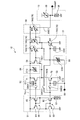
- FIG. 3 is an explanatory diagram of a configuration example of the PSRR correction circuit.
- the PSRR correction circuit is configured as shown in FIG. 3 so that low power consumption and highly accurate noise correction can be realized.
- the PSRR correction circuit 12 includes a fixed conductance bias unit 51, a bias unit 52, an input sensing unit 53, a lag phase adjustment unit 54, a leading phase adjustment unit 55, a transistor 56, a gain switching / inversion circuit 31, A gain adjuster 58 and a pixel power input terminal (noise monitor terminal) 59 are provided. Since the PSRR correction circuit having the same characteristics can take a plurality of forms (configurations), specific circuits before and after the gain switching / inversion circuit 31 may have a configuration different from that in FIG.
- the fixed conductance bias unit 51 includes a first current mirror circuit 63 including an N-channel MOS transistor 61 and an N-channel MOS transistor 62, a second current mirror circuit 66 including a P-channel MOS transistor 64 and a P-channel MOS transistor 65, and , A pull-up resistor 67, and applies a fixed bias voltage to the bias unit 52, the input sense unit 53, and the gain switching / inverting circuit 31.
- the current amount of the N-channel MOS transistor 62 is m times the current amount of the N-channel MOS transistor 61.
- the gate terminals of N-channel MOS transistor 61 and N-channel MOS transistor 62 are connected to each other.
- the source terminal of the N-channel MOS transistor 61 is grounded, and the drain terminal of the N-channel MOS transistor 61 is connected to the gate terminal of the N-channel MOS transistor 61.
- the source terminal of N-channel MOS transistor 62 is grounded via pull-up resistor 67.
- the sizes of the P-channel MOS transistor 64 and the P-channel MOS transistor 65 are the same. Further, the gate terminal of the P-channel MOS transistor 65 is connected to the gate terminal of the P-channel MOS transistor 64.
- the source terminal of the P-channel MOS transistor 64 is connected to the power supply VDDH , and the drain terminal of the P-channel MOS transistor 64 is connected to the drain terminal of the N-channel MOS transistor 61.
- the power supply VDDH may be a pixel power supply or another power supply different from the pixel power supply.
- the source terminal of the P-channel MOS transistor 65 is connected to the power supply VDDH , and the drain terminal of the P-channel MOS transistor 65 is connected to the drain terminal of the N-channel MOS transistor 62.
- the drain terminal of the P-channel MOS transistor 65 is also connected to the gate terminal of the P-channel MOS transistor 65.
- the conductance of the N-channel MOS transistor 61 is constant, and the conductance is the ratio m of the parallel number of the N-channel MOS transistor 61 and the N-channel MOS transistor 62. And the resistance value of the pull-up resistor 67.
- the bias unit 52 includes a P-channel MOS transistor 71, a switch SW21, and a capacitor (capacitance element) C11.
- the drain terminal of the P-channel MOS transistor 71 is connected to the power supply VDDH , and the gate terminal of the P-channel MOS transistor 71 is connected to the power supply VDDH via the capacitor C11. Further, the gate terminal of the P-channel MOS transistor 71 is connected to the gate terminals of the P-channel MOS transistors 64 and 65 of the conductance fixed bias unit 51 via the switch SW21.
- the P-channel MOS transistor 71 functions as a current source, and a common connection point between the drain terminal of the P-channel MOS transistor 71 and the drain terminal of the N-channel MOS transistor 72 and the P-channel MOS transistor 56 is provided. An electric current always flows such that the conductance of the N-channel MOS transistor 72 of the input sense unit 53 becomes a constant value.
- the input sensing unit 53 includes an N-channel MOS transistor 72, a switch SW23, and a capacitor (capacitance element) C12.
- the source terminal of the N-channel MOS transistor 71 is grounded, and the gate terminal of the N-channel MOS transistor 71 is connected to the pixel power input terminal via the capacitor C12.
- the gate terminal of the N-channel MOS transistor 71 is connected to the gate terminals of the N-channel MOS transistors 61 and 62 of the fixed conductance bias unit 51 via a switch SW23 used for sample and hold.
- the drain terminal of the N-channel MOS transistor 72 is connected to the bias unit 52 and the lag phase adjuster 54. Further, the drain terminal of the N-channel MOS transistor 72 is connected to the gate terminal of the P-channel MOS transistor 56.
- the gate of the N-channel MOS transistor 72 is turned on.
- the operating point of the terminal is determined. That is, in such a state, a current corresponding to the current flowing through the N-channel MOS transistor 61 of the fixed conductance bias unit 51 flows through the N-channel MOS transistor 72.
- the AC component of the power supply noise detected at the pixel power supply input terminal 59 is extracted by the capacitor C12 functioning as a high-pass filter and input to the gate terminal of the N-channel MOS transistor 72.
- the N-channel MOS transistor 72 receives a current including an AC component corresponding to the AC (alternating current) component of the pixel power supply noise included in the pixel power supply and a DC component determined by the N-channel MOS transistor 61.
- the power supply noise as a voltage signal is converted into a noise cancellation signal NC0 which is a current signal.
- the conductance of the N-channel MOS transistor 61 is always constant (fixed), the conductance of the N-channel MOS transistor 72 is also constant.
- the conductance of the N-channel MOS transistor 72 of the input sense unit 53 is constant from the drain terminal of the P-channel MOS transistor 71 to the common connection point of the drain terminal of the N-channel MOS transistor 72 and the P-channel MOS transistor 56. A current that is a value always flows.
- the current flowing on the P-channel MOS transistor 56 side is changed from the noise cancellation signal NC0 flowing through the N-channel MOS transistor 72 of the input sense unit 53 to the drain terminal of the N-channel MOS transistor 72 from the P-channel MOS transistor 71 of the bias unit 52. This is obtained by subtracting the current flowing to the common connection point of the P-channel MOS transistors 56.
- ⁇ That is, the current flowing on the P-channel MOS transistor 56 side is a noise cancellation signal NC1 (corresponding to a first noise cancellation signal) in which a DC component is partially removed from the noise cancellation signal NC0 by the bias unit 52.
- the switch SW21 is in a closed state (ON state) during a period in which noise is not canceled, and the switch SW21 is in an open state (OFF state) during a period in which noise is canceled.
- the output noise of the fixed conductance bias unit 51 is connected to the drain terminal of the N-channel MOS transistor 72 via the P-channel MOS transistor 71 and the P-channel MOS transistor. It is output to the common connection point of the channel MOS transistors 56 and can be prevented from being superimposed on the noise cancel signal NC1. Note that the switch SW21 is not necessarily required to be provided.
- the delay phase adjuster 54 includes a variable capacitor C13 provided between the power supply VDDH , the drain terminal of the N-channel MOS transistor 72, and a common connection point of the P-channel MOS transistor 56.
- the lag phase adjuster 54 adjusts the lag phase of the high-frequency component of the noise cancellation signal, which is the current flowing from the P-channel MOS transistor 56 to the common connection point of the drain terminal of the N-channel MOS transistor 72 and the P-channel MOS transistor 56. .
- variable capacitor C13 of the delay phase adjuster 54 functions as a low-pass filter, and adjusts the phase by attenuating (the gain of) the AC component of the noise cancellation signal, that is, adjusts the delay phase.
- the cutoff frequency of the low-pass filter is determined by the capacitance of the variable capacitor C13 and the resistance component of the P-channel MOS transistor 56.
- the advance phase adjuster 55 includes a variable capacitor C14 connected between the pixel power input terminal 59 and the gain switching / inverting circuit 31.
- the advanced phase adjuster 55 adjusts the advanced phase of the noise cancel signal NC1, which is a current flowing from the common connection point of the drain terminal of the N-channel MOS transistor 72 and the P-channel MOS transistor 56 to the gain switching / inverting circuit 31, in a high frequency range. I do.
- the high-pass component is propagated to the gain switching / inversion circuit 31 by connecting the gain switching / inversion circuit 31 and the pixel power supply via the variable capacitor C14.
- variable capacitor C14 of the advance phase adjustment unit 55 functions as a high-pass filter, and performs the phase adjustment, that is, the advance phase adjustment by superimposing the high frequency component of the pixel power supply noise on the gain switching / inversion circuit 31.
- the cutoff frequency as a high-pass filter is determined by the capacitance of the variable capacitor C14 and the apparent resistance of the gain switching / inverting circuit 31.
- the gate terminal is commonly connected to the gate terminal of the P-channel MOS transistor 56, the source terminal is commonly connected to the power supply VDD , and the drain terminal is advanced and is common to the variable capacitor C14 of the phase adjustment unit 55.
- a P-channel MOS transistor group 73G including a plurality of connected P-channel MOS transistors 73 connected in parallel is provided.
- the gain switching / inverting circuit 31 has a source terminal commonly connected to the power supply VDD , a drain terminal commonly connected to a commonly connected drain terminal of the P-channel MOS transistor group 73G, and a gate terminal for switching the number of connections (not shown).
- a P-channel MOS transistor group 74G composed of a plurality of P-channel MOS transistors 74 commonly connected to the drain terminal via a switch is provided.
- the gain switching / inverting circuit 31 has a drain terminal connected to a common connection point between the commonly connected drain terminal of the P-channel MOS transistor group 73G and the commonly connected drain terminal of the P-channel MOS transistor group 74G, and a source terminal.
- the commonly connected gate terminal is connected to the gate terminal of the N-channel MOS transistor 61 of the fixed conductance bias unit 51 via the switch SW22, and is constituted by a plurality of N-channel MOS transistors 75 connected in parallel.
- an N-channel MOS transistor group 75G functioning as a current source, and a capacitor C15 having one end connected to the commonly connected gate terminal of the N-channel MOS transistor group 75G and the other end grounded. I have.
- the number of P-channel MOS transistors 73 actually operated (the number of parallel P-channel MOS transistors 73)
- the number of P-channel MOS transistors 74 actually operated the parallel number of P-channel MOS transistors 74
- the number of N-channel MOS transistors 75 actually operated (parallel number of N-channel MOS transistors 75) among a plurality of parallel-connected N-channel MOS transistors 75 forming the MOS transistor group 75G is determined by the ULV And it is possible to switch in conjunction with the input capacitance switching the regulator, it has become effectively can perform gain switching of PSRR correction circuit 12.
- the detailed gain switching in the gain switching / inverting circuit 31 will be described later in detail.
- the configuration of the gain switching / inverting circuit 31 is an example, and the present invention can be similarly applied to another circuit having a function of inverting the polarity of a waveform and a function of switching a gain.
- the gain adjuster 58 is connected in parallel to a plurality of commonly connected gate terminals of a plurality of parallel-connected P-channel MOS transistors constituting the P-channel MOS transistor group 74 via a connection number changeover switch (not shown).
- a plurality of P-channel MOS transistors 76 have a gate terminal commonly connected, a source terminal commonly connected to the power supply VDD , and a drain terminal commonly connected to a connection point between the variable current source 35 and the output resistor 36 of the DA converter 13.
- a P-channel MOS transistor group 76G including P-channel MOS transistors 76 connected in parallel is provided.
- the gain adjuster 58 adjusts the number of parallel P-channel MOS transistors actually driven so that the noise signal and the noise cancel signal are appropriately canceled in the ULV comparator 14 (P-channel MOS transistor group). By changing the number of outputs of the multi-output current mirror formed by cooperating with 74, the gain is finely adjusted in accordance with the amplitude of the power supply noise signal.
- the operation of the gain switching / inversion circuit 31 will be described. Since the P-channel MOS transistor group 73G of the gain switching / inverting circuit 31 functions as a multi-output type current mirror circuit in cooperation with the P-channel MOS transistor 56, the current flowing through the P-channel MOS transistor 56 by the noise cancel signal NC1. (A current having the same polarity and a size ratio corresponding to the size ratio of the transistors) flows between the source terminal and the drain terminal of the P-channel MOS transistors 73 constituting the P-channel MOS transistor group 73G. Becomes
- the P-channel MOS transistor group 73G is formed, the current flowing between the source terminal and the drain terminal of the plurality of P-channel MOS transistors 73 that are actually operating, and the P-channel MOS transistor group 74G are formed.
- the sum of the current flowing between the source terminal and the drain terminal of the plurality of operating P-channel MOS transistors 74 constitutes an N-channel MOS transistor group 75G functioning as a current source. It is equal to the current flowing between the drain terminal and the source terminal of the N-channel MOS transistor 75.
- the current flowing through the P channel MOS transistor group 74G is equal to the current obtained by subtracting the current flowing through the P channel MOS transistor group 73G from the current flowing through the N channel MOS transistor group 75G.
- the current flowing through P-channel MOS transistor group 74G has a polarity opposite to the current corresponding to noise cancel signal NC1 flowing through P-channel MOS transistor group 73G.
- the noise canceling signal whose gain has been switched and whose polarity has been inverted (hereinafter, referred to as an inverted polarity noise canceling signal XNC1 and corresponds to a second noise canceling signal) is supplied to the DA converter 13 as a final noise canceling signal. .
- the gain control unit 15 of the solid-state imaging device 10 switches both the slope of the ramp signal RAMP as a reference signal output from the DA converter and the input capacitance of the input capacitance variable unit 41 of the ULV comparator 14. .
- the input capacitance of the pixel signal VSL and the input capacitance of the ramp signal RAMP are arranged on the same side as a differential pair.
- the amount of attenuation until reaching the pair becomes larger than that of the conventional comparator due to the capacitance partial pressure.
- the noise of the transistor is effectively increased in terms of the pixel signal VSL.
- the amount of attenuation of the pixel signal VSL before reaching the differential pair can be reduced, and noise deterioration can be suppressed.
- the gain control unit 15 increases the input capacitance C_RAMP on the side of the ramp signal RAMP, and The input capacitance C_VSL on the signal VSL side is reduced.
- the gain control unit 15 decreases the input capacitance on the side of the ramp signal RAMP and decreases the input capacitance on the side of the pixel signal VSL. To increase.
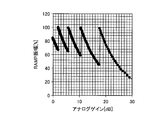
- FIG. 4 is a diagram illustrating the relationship between the gain of the single slope AD converter and the amplitude of the ramp signal.
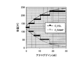
- FIG. 5 is an explanatory diagram showing the relationship between the input capacitance on the ramp signal side, the input capacitance on the pixel signal side, and the gain of the single slope AD converter.
- the gain control unit 15 sets the control signal of each unit in accordance with the gain setting of the single-slope AD converter 17, thereby switching the input capacitance stepwise, and also switching the amplitude of the ramp signal RAMP accordingly. By doing so, the deterioration of noise is minimized.
- the gain control unit 15 controls the gain switching / inversion circuit 31 of the PSRR correction circuit 12 at the same time, and changes the gain of the PSRR correction circuit according to the switching of the capacity (input capacity) of the input capacity variable unit 41 of the ULV comparator 14. Switch.
- the gain control unit 15 controls the gain switching / inversion circuit 31 and, in parallel, among the P-channel MOS transistors 73 constituting the P-channel MOS transistor group 73G of the gain switching / inversion circuit 31, The number of P-channel MOS transistors 73 to be connected and actually driven is controlled.
- the number of P-channel MOS transistors 74 constituting the P-channel MOS transistor group 74G is controlled to form the N-channel MOS transistor group 75G.
- the number of N-channel MOS transistors 75 that are connected in parallel and are actually driven among the N-channel MOS transistors 75 that are being driven is controlled.
- the P-channel MOS transistor group 73G is formed, the current flowing between the source terminal and the drain terminal of the plurality of P-channel MOS transistors 73 that are actually operating, and the P-channel MOS transistor group 74G are formed.
- the sum of the current flowing between the source terminal and the drain terminal of the plurality of operating P-channel MOS transistors 74 constitutes an N-channel MOS transistor group 75G functioning as a current source, and the plurality of actually operating plurality of The current is equal to the current flowing between the drain terminal and the source terminal of the N-channel MOS transistor 75.
- the PSRR correction circuit 12 monitors generation of power supply noise in the pixel power supply GPW, and cancels (corrects) power supply noise based on the power supply noise generated in the pixel power supply GPW.
- a noise cancel signal XNC1 is generated and output to the DA converter 13.
- the DA converter 13 generates a ramp signal RAMP, which is a reference signal whose waveform (voltage value) changes in a time-wise slope manner, and outputs the ramp signal RAMP to the ULV comparator 14. Therefore, the ramp signal RAMP output from the DA converter 13 includes the noise cancel signal XNC1 having the opposite polarity to the noise signal of the pixel power supply.
- the PSRR correction circuit 12 cancels the power supply noise in the ULV comparator 14 by inputting the generated noise cancel signal XNC1 to the ULV comparator 14 via the DA converter 13.
- the ramp signal RAMP which is the reference signal on which the noise cancel signal XNC1 is superimposed, is input to the ULV comparator 14, so that when the ramp signal RAMP is compared with the pixel signal VSL from the pixel 11, The power supply noise of the pixel power supply GPW superimposed on the pixel signal VSL is canceled by the noise cancel signal XNC1.
- the single-slope AD converter 17 effectively outputs the A / D conversion result of the pixel signal VSL (after canceling the noise of the pixel power supply) as a digital pixel signal.
- the power supply noise can be canceled with high accuracy with a simpler configuration, and thereby, a higher quality image can be obtained. Further, according to the solid-state imaging device 10, low power consumption can be realized.
- FIG. 6 is an explanatory diagram of an example of a floor plan of the image sensor. Although various floor plans of the image sensor are conceivable, a pixel array unit 81 in which a plurality of pixels 11 are arranged is arranged on the upper chip UC.
- the lower chip LC includes, in addition to the PSRR correction circuit 12, the DA converter 13, the ultra-low voltage (ULV) comparator 14, the gain control unit 15, the load MOS transistor 16, and the read control of the pixel array unit 81.
- the solid-state imaging device 10 includes a pixel control circuit 82 for performing the operation, a logic block 83 that performs various controls and image processing of the entire solid-state imaging device 10, and an interface unit 84 that performs various interface operations. .
- the PSRR correction circuit 12 needs to supply a current corresponding to the noise cancel signal XNC1 to the output resistor 36 constituting the DA converter 13, so that noise mixed due to an increase in the wiring length is mixed. In order to reduce the influence of changes in frequency and frequency characteristics, it is preferable to dispose it adjacent to the DA converter 13.
- a plurality of ULV comparators 14 constituting the single-slope AD converter 17 are arranged at upper and lower portions in FIG. 6 of the lower chip LC, respectively, from the pixels 11 constituting the pixel array portion 81 of the upper chip UC. Since the pixel signal VSL is respectively input, the DA converter 13 which needs to supply the ramp signal RAMP to the plurality of ULV comparators 14 is preferably arranged at the center of the lower chip.
- imaging device ⁇ Configuration example of imaging device> Furthermore, the present technology is applicable to all electronic devices that use an imaging device for a photoelectric conversion unit, such as imaging devices such as digital still cameras and video cameras, portable terminal devices having an imaging function, and copiers that use an imaging device for an image reading unit. Applicable to
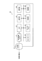
- FIG. 7 is a diagram illustrating a configuration example of an imaging device as another electronic device.
- the imaging device 90 includes an optical system 91 including a lens group, a solid-state imaging device 10, a DSP (Digital Signal Processor) 92 as a signal processing circuit for processing imaging data, a liquid crystal display, an organic EL display, and the like.
- a display unit 93 configured to display a captured image and various information, an operation unit 94 for a user to perform various operations such as an imaging instruction and data setting, a controller 95 for controlling the entire imaging device 90, and store image data.
- a frame memory 96, a recording unit 97 for recording imaging data on a recording medium such as a hard disk and a memory card (not shown), and a power supply unit 98 for supplying power to the entire imaging device 90 are provided.
- the DSP 92, the display unit 93, the operation unit 94, the controller 95, the frame memory 96, the recording unit 97, and the power supply unit 98 are connected to each other via a bus line.
- the above-described solid-state imaging device 10 is used as an imaging device, a clear and high-quality image with low noise and low noise can be captured for a long time with low power consumption.
- Examples of the actual mode of the imaging device 90 include a camera module for a mobile terminal device such as a video camera, a digital still camera, and a smartphone.
- FIG. 8 is a diagram illustrating a configuration example of an imaging device as still another electronic device.
- the imaging device 100 includes an optical system 101 including a lens group, a solid-state imaging device 10, a DSP 102 as a signal processing circuit for processing imaging data, and an interface unit 103 for performing an interface operation with an external device 110. And a frame memory 104 for storing image data.
- the imaging device 100 of the present embodiment is configured to perform imaging under the control of the external device 110 by a power supply supplied from the external device 110.
- a power supply supplied from the external device 110 For example, under the control of an in-vehicle ECU or the like as the external device 110, The present invention can be applied to a camera module or the like that captures a monitoring image around the vehicle by receiving power supply from the vehicle.
- the external device 110 performs image processing on the interface unit 111 that performs an interface operation with the imaging apparatus 100 and the image data acquired via the interface unit 111, and performs the desired image data (for example, An image processing unit 112 that performs image processing for obtaining an obstacle image, a sign recognition image, and the like), a power supply unit 113 that supplies power for operation to the imaging device 100 and the external device 110, and control of the imaging device 100.
- the imaging device 100 is provided on a peripheral surface (a front surface, a side surface, a rear surface) of a vehicle, a vehicle interior, or the like for ensuring safe driving such as automatic stop, recognizing a driver's state, and the like.
- a peripheral surface a front surface, a side surface, a rear surface
- Examples include an in-vehicle sensor for photographing the inside of a vehicle, a surveillance camera for remotely monitoring a running vehicle and a road, and a distance measuring device.
- the main body of a home electric appliance can be used as the external device 110 as an imaging device for detecting and controlling the position, operation (gesture), and the like of the user. Further, it can be used for person authentication, skin photographing, and the like.
- the present invention can also be used as an imaging device for infrared rays, ultraviolet rays, X-rays, and the like.
- a pixel that outputs a pixel signal
- a first noise canceling signal that is connected to a pixel power supply that supplies power to the pixel, cancels power supply noise of the pixel power supply, and performs gain switching based on a gain control signal with respect to the first noise canceling signal
- a noise cancellation signal generation circuit that performs polarity inversion and outputs the second noise cancellation signal, a DA converter that generates and outputs a reference signal that is a ramp signal, and that converts the current of the second noise cancellation signal into a voltage and superimposes it on the ramp signal
- a comparator that inputs the reference signal and the pixel signal to the comparator main body through an input capacitor connected to one terminal of the differential pair, and outputs an inverted signal having a timing according to the pixel signal and a gain setting
- a counter for converting the inversion timing of the comparator into a digital value, When changing the slope of the reference signal and the input capacitance to perform gain control of the comparator,
- the noise cancellation signal generation circuit a pixel power supply input unit to which the pixel power supply is connected, A first noise cancellation signal generation unit that converts the pixel power supply voltage input through the pixel power input unit into a current to generate the first noise cancellation signal; A gain switching / inversion circuit that performs gain switching and polarity inversion of the first noise cancellation signal based on the gain control signal;
- the solid-state imaging device comprising: (4)
- the gain switching / inverting circuit includes a first transistor group including a plurality of transistors connected in parallel and capable of flowing a current amount proportional to a current amount of the first noise cancellation signal; A second transistor group composed of a plurality of transistors connected in parallel to each other and connected in parallel to each other and capable of passing a predetermined constant current; and a second transistor group connected in parallel to the first transistor group.
- a third transistor group capable of outputting a cancel signal.
- a fourth transistor group that forms a current mirror circuit with the third transistor group and that can adjust and output the gain of the second noise cancellation signal;
- (6) The solid-state imaging device according to any one of (3) to (5), wherein the gain switching / inverting circuit and the DA converter are disposed adjacent to or adjacent to each other.
- the comparator is arranged at a peripheral portion of the chip,
- the DA converter is arranged in a central portion of the chip.
- a pixel array section in which a plurality of pixels each outputting a pixel signal are arranged in an array, A first noise canceling signal is connected to a pixel power supply that supplies power to the pixel, and cancels a power supply noise of the pixel power supply.
- a noise cancel signal generation circuit that performs polarity inversion and outputs the result as a second noise cancel signal; a DA converter that generates and outputs a reference signal that is a ramp signal, and that converts the current of the second noise cancellation signal into a voltage and superimposes the voltage on the ramp signal; A comparator that inputs the reference signal and the pixel signal to the comparator main body via an input capacitor connected to one terminal of the differential pair, and outputs an inverted signal having a timing according to the pixel signal and a gain setting; A counter for converting the inversion timing of the comparator into a digital value; A gain control unit that outputs the gain control signal based on a change amount of the input capacitance when performing the gain control of the comparator by changing the slope of the reference signal and the input capacitance; An image data processing unit that performs processing of image data based on the output of the counter, Electronic equipment with.
Landscapes
- Engineering & Computer Science (AREA)
- Multimedia (AREA)
- Signal Processing (AREA)
- Theoretical Computer Science (AREA)
- Physics & Mathematics (AREA)
- Nonlinear Science (AREA)
- Electromagnetism (AREA)
- Transforming Light Signals Into Electric Signals (AREA)
- Analogue/Digital Conversion (AREA)
- Manipulation Of Pulses (AREA)
Abstract
Description
コンパレータは、参照信号及び画素信号が差動対の一方の端子に接続された入力容量を介してコンパレータ本体に入力され、画素信号とゲイン設定に応じたタイミングを持つ反転信号をカウンタに出力する。
カウンタは、コンパレータの反転タイミングをディジタル値に変換して出力する。
図1は、実施形態の固体撮像素子の一例を示す概要構成図である。
実施形態の固体撮像素子としては、CCDイメージセンサ、CMOSイメージセンサ等が挙げられる。
例えば、画素11は、図1に示すように、フォトダイオード21、転送トランジスタ22、浮遊拡散領域23、増幅トランジスタ24、選択トランジスタ25及びリセットトランジスタ26を備えている。
この画素11は、撮像素子に設けられた後述の画素アレイ部を構成する画素の数(上述の例の場合、N×M個)だけ設けられているが、理解の容易のため、図1においては、一つだけ記載している。
また、増幅トランジスタ24のドレイン端子は、画素電源GPWに接続され、ソース端子は、選択トランジスタ25のドレイン端子に接続されている。
撮像時には、固体撮像素子10に入射した光がフォトダイオード21により受光されて光電変換され、その結果得られた電荷がフォトダイオード21に蓄積される。そして、転送トランジスタ22のゲートに電圧が印加されて閉状態(オン状態)とされると、フォトダイオード21と浮遊拡散領域23が電気的に接続され、フォトダイオード21の電荷が転送トランジスタ22を介して浮遊拡散領域23に転送され、増幅トランジスタ24のゲートに信号電圧が生じる。
ここで、PSRR補正回路12が設けられている理由について説明する。
固体撮像素子10においては、画素電源GPWからの電源ノイズが、画素内の各ノード間につく図示しない寄生容量や増幅トランジスタ24や選択トランジスタ25を介して垂直信号線VSLに伝搬される。
ゲイン切替/反転回路31の構成については、後に詳述する。
ディジタル値によって可変電流源35を制御されたDA変換器13の出力は、時間と共に信号レベルが変化するランプ(ramp)信号であり、画素11から出力された画素信号をA/D(Analog to Digital)変換するための参照信号として機能する。
図2は、ULVコンパレータの回路構成例の説明図である。
ULVコンパレータ14は、大別すると、対応する画素11が出力した画素信号VSLが入力される画素信号入力端子TTV及びDA変換器13が出力したramp信号RAMPが入力される参照信号入力端子TTRを有する入力容量可変部41と、コンパレータ本体部42と、基準電圧保持コンデンサ43と、を備えている。
図3は、PSRR補正回路の構成例の説明図である。
本実施形態では、PSRR補正回路を図3に示すような構成とすることで、低消費電力化と、高精度なノイズ補正を実現できるようにした。
さらにPチャネルMOSトランジスタ71のゲート端子は、スイッチSW21を介して、コンダクタンス固定バイアス部51のPチャネルMOSトランジスタ64、65のゲート端子に接続されている。
されにNチャネルMOSトランジスタ71のゲート端子は、サンプルホールド用に用いられるスイッチSW23を介して、コンダクタンス固定バイアス部51のNチャネルMOSトランジスタ61、62のゲート端子に接続されている。
そして、NチャネルMOSトランジスタ72には、画素電源に含まれる画素電源ノイズのAC(交流)成分に応じたAC成分と、NチャネルMOSトランジスタ61により定まるDC成分と、を含む電流がノイズキャンセル信号NC0として流れ、電圧信号としての電源ノイズが、電流信号であるノイズキャンセル信号NC0へと変換される。
遅れ位相調整部54は、PチャネルMOSトランジスタ56からNチャネルMOSトランジスタ72のドレイン端子とPチャネルMOSトランジスタ56の共通接続点へと流れる電流であるノイズキャンセル信号の高域成分の遅れ位相を調整する。
進み位相調整部55は、NチャネルMOSトランジスタ72のドレイン端子とPチャネルMOSトランジスタ56の共通接続点からゲイン切替/反転回路31へと流れる電流であるノイズキャンセル信号NC1の高域における進み位相を調整する。
なお、ゲイン切替/反転回路31の構成は一例であり、波形の極性反転とゲイン切替機能を有する他の回路であっても同様に適用が可能である。
ゲイン切替/反転回路31のPチャネルMOSトランジスタ群73Gは、PチャネルMOSトランジスタ56と共働して、多出力型カレントミラー回路として機能するので、ノイズキャンセル信号NC1によりPチャネルMOSトランジスタ56を流れる電流に比例した電流(同極性で大きさの比がトランジスタのサイズ比に相当する電流)がPチャネルMOSトランジスタ群73Gを構成しているPチャネルMOSトランジスタ73のソース端子-ドレイン端子間をそれぞれ流れることとなる。
そして、ゲイン切替及び極性が反転されたノイズキャンセル信号(以下、逆極性ノイズキャンセル信号XNC1という。第2ノイズキャンセル信号に相当。)は、最終的なノイズキャンセル信号としてDA変換器13に供給される。
固体撮像素子10のゲイン制御部15は、ゲイン制御を行うにあたって、DA変換器の出力する参照信号としてのramp信号RAMPのスロープ傾き及びULVコンパレータ14の入力容量可変部41の入力容量の双方を切り替える。
図4は、シングルスロープAD変換器のゲインとramp信号の振幅の関係説明図である。
図5は、ramp信号側の入力容量及び画素信号側の入力容量とシングルスロープAD変換器のゲインとの関係説明図である。
なお、シングルスロープAD変換器17のゲインが極端に低い場合には、ノイズキャンセル効果は低下するが、帯域調整などを行うことでノイズを抑制することが可能である。
したがって、DA変換器13から出力されるramp信号RAMPには、画素電源のノイズ信号とは逆極性のノイズキャンセル信号XNC1が含まれている。
図6は、撮像素子のフロアプランの一例の説明図である。
撮像素子のフロアプランは様々考えられるが、上チップUCには、複数の画素11が配置された画素アレイ部81を配置している。
さらに、本技術は、デジタルスチルカメラやビデオカメラ等の撮像装置や、撮像機能を有する携帯端末装置や、画像読取部に撮像素子を用いる複写機など、光電変換部に撮像素子を用いる電子機器全般に対して適用可能である。
撮像装置90は、レンズ群などを備えた光学系91と、固体撮像素子10と、撮像データを処理をする信号処理回路としてのDSP(Digital Signal Processor)92と、液晶ディスプレイ、有機ELディスプレイ等で構成され撮像画像、各種情報を表示する表示部93と、ユーザが撮像指示、データ設定等の各種操作を行う操作部94と、撮像装置90全体の制御を行うコントローラ95と、画像データを格納するフレームメモリ96と、図示しないハードディスク、メモリカード等の記録媒体に対し撮像データの記録を行う記録部97と、撮像装置90全体に電力を供給する電源部98と、を備えている。
撮像装置90の実際の態様としては、ビデオカメラ、デジタルスチルカメラ、スマートフォン等のモバイル端末装置向けのカメラモジュールなどが挙げられる。
撮像装置100は、レンズ群などを備えた光学系101と、固体撮像素子10と、撮像データを処理をする信号処理回路としてのDSP102と、外部機器110との間でインタフェース動作を行うインタフェース部103と、画像データを格納するフレームメモリ104と、を備えている。
さらに人物認証用、肌撮影用等に用いることも可能である。
(1)
画素信号を出力する画素と、
前記画素に電力を供給する画素電源に接続され、前記画素電源の電源ノイズをキャンセルするための第1ノイズキャンセル信号を生成し、前記第1ノイズキャンセル信号に対し、ゲイン制御信号に基づくゲイン切替及び極性反転を行って第2ノイズキャンセル信号として出力するノイズキャンセル信号生成回路と、
ramp信号である参照信号を生成し出力すると共に前記第2ノイズキャンセル信号の電流を電圧に変えてramp信号に重畳させるDA変換器と、
前記参照信号及び前記画素信号が差動対の一方の端子に接続された入力容量を介してコンパレータ本体に入力され、画素信号とゲイン設定に応じたタイミングを持つ反転信号を出力するコンパレータと、
コンパレータの反転タイミングをディジタル値に変換するカウンタと、
前記参照信号の傾き及び前記入力容量を変更して前記コンパレータのゲイン制御を行うに際し、前記入力容量の変更量に基づく前記ゲイン制御信号を出力するゲイン制御部と、
を備えた固体撮像素子。
(2)
コンパレータは、入力端子と前記差動対の一方の端子との間に接続された第1のコンデンサと、
前記差動対の一方の端子に一端が接続された複数の第2コンデンサと、
前記第2コンデンサを前記第1のコンデンサと並列に接続するための複数のスイッチと、
を有する入力容量切替部を備えた、
(1)記載の固体撮像素子。
(3)
前記ノイズキャンセル信号生成回路は、前記画素電源が接続される画素電源入力部と、
前記画素電源入力部を介して入力された画素電源電圧を電流に変換して前記第1ノイズキャンセル信号を生成する第1ノイズキャンセル信号生成部と、
前記ゲイン制御信号に基づいて前記第1ノイズキャンセル信号のゲイン切替及び極性反転を行うゲイン切替/反転回路と、
を備えた(1)又は(2)記載の固体撮像素子。
(4)
前記ゲイン切替/反転回路は、前記第1ノイズキャンセル信号の電流量に比例する電流量を流すことが可能な互いに並列接続された複数のトランジスタで構成された第1トランジスタ群と、前記第1トランジスタ群に直列に接続され、所定の定電流を流すことが可能な互いに並列接続された複数のトランジスタで構成された第2トランジスタ群と、前記第1トランジスタ群に並列に接続され、前記第2ノイズキャンセル信号を出力可能な第3トランジスタ群と、を備える、
(3)記載の固体撮像素子。
(5)
前記第3トランジスタ群と、カレントミラー回路を構成し、前記第2ノイズキャンセル信号のゲインを調整して出力可能な第4トランジスタ群を備える、
(4)記載の固体撮像素子。
(6)
前記ゲイン切替/反転回路と、DA変換器とは、隣設あるいは近接して配置されている、(3)乃至(5)のいずれか一項記載の固体撮像素子。
(7)
前記コンパレータは、チップの周縁部に配置され、
前記DA変換器は、チップの中央部に配置されている、
(1)乃至(6)のいずれか一項記載の固体撮像素子。
(8)
画素信号をそれぞれ出力する複数の画素がアレイ状に配置された画素アレイ部と、
前記画素に電力を供給する画素電源に接続され、前記画素電源の電源ノイズをキャンセルするための第1ノイズキャンセル信号を生成し、前記第1ノイズキャンセル信号に対し、ゲイン制御信号に基づくゲイン切替及び極性反転を行って第2ノイズキャンセル信号として出力するノイズキャンセル信号生成回路と、
ramp信号である参照信号を生成し出力すると共に前記第2ノイズキャンセル信号の電流を電圧に変えてramp信号に重畳させるDA変換器と、
前記参照信号及び前記画素信号が差動対の一方の端子に接続された入力容量を介してコンパレータ本体に入力され、画素信号とゲイン設定に応じたタイミングを持つ反転信号を出力するコンパレータと、
前記コンパレータの反転タイミングをディジタル値に変換するカウンタと、
前記参照信号の傾き及び前記入力容量を変更して前記コンパレータのゲイン制御を行うに際し、前記入力容量の変更量に基づく前記ゲイン制御信号を出力するゲイン制御部と、
前記カウンタの出力に基づいて画像データの処理を行う画像データ処理部と、
を備えた電子機器。
11 画素
12 PSRR補正回路
13 DA変換器
14 ULVコンパレータ
15 ゲイン制御部
16 負荷MOSトランジスタ
17 シングルスロープAD変換器
18 カウンタ
21 フォトダイオード
22 転送トランジスタ
23 浮遊拡散領域
24 増幅トランジスタ
25 選択トランジスタ
31 ゲイン切替/反転回路
35 可変電流源
36 出力抵抗
41 入力容量可変部
42 コンパレータ本体部
43 基準電圧保持コンデンサ
51 コンダクタンス固定バイアス部
52 バイアス部
53 入力センス部
54 位相調整部
55 位相調整部
56 PチャネルMOSトランジスタ
58 ゲイン調整部
59 画素電源入力端子
73 NチャネルMOSトランジスタ
73G PチャネルMOSトランジスタ群
74 PチャネルMOSトランジスタ
74 PチャネルMOSトランジスタ群
74G PチャネルMOSトランジスタ群
75 NチャネルMOSトランジスタ
75G NチャネルMOSトランジスタ群
76 PチャネルMOSトランジスタ
76G PチャネルMOSトランジスタ群
C11、C12、C15 コンデンサ
C13、C14 可変容量コンデンサ
GC1~GC3 ゲイン制御信号
GPW 画素電源
LC 下チップ
LG 画素側電流ライン
LR 参照側電流ライン
NC0 ノイズキャンセル信号
NC1 ノイズキャンセル信号(第1ノイズキャンセル信号)
PRC 画像データ処理部
PW 電源部
RAMP ramp信号
SW1~SW5 スイッチ
TIN 画素側入力端子
TTR 参照信号入力端子
TTV 画素信号入力端子
UC 上チップ
VSL 垂直信号線、画素信号
XNC1 逆極性ノイズキャンセル信号(第2ノイズキャンセル信号)
Claims (6)
- 画素信号を出力する画素と、
前記画素に電力を供給する画素電源に接続され、前記画素電源の電源ノイズをキャンセルするための第1ノイズキャンセル信号を生成し、前記第1ノイズキャンセル信号に対し、ゲイン制御信号に基づくゲイン切替及び極性反転を行って第2ノイズキャンセル信号として出力するノイズキャンセル信号生成回路と、
ramp信号である参照信号を生成し出力すると共に前記第2ノイズキャンセル信号の電流を電圧に変えて前記参照信号に重畳させるDA変換器と、
前記参照信号及び前記画素信号が差動対の一方の端子に接続された入力容量を介してコンパレータ本体に入力され、画素信号とゲイン設定に応じたタイミングを持つ反転信号を出力するコンパレータと、
前記コンパレータの反転タイミングをディジタル値に変換するカウンタと、
前記参照信号の傾き及び前記入力容量を変更して前記コンパレータのゲイン制御を行うに際し、前記入力容量の変更量に基づく前記ゲイン制御信号を出力するゲイン制御部と、
を備えた固体撮像素子。 - コンパレータは、入力端子と前記差動対の一方の端子との間に接続された第1のコンデンサと、
前記差動対の一方の端子に一端が接続された複数の第2コンデンサと、
前記第2コンデンサを前記第1のコンデンサと並列に接続するための複数のスイッチと、
を有する入力容量切替部を備えた、
請求項1記載の固体撮像素子。 - 前記ノイズキャンセル信号生成回路は、前記画素電源が接続される画素電源入力部と、
前記画素電源入力部を介して入力された画素電源電圧を電流に変換して前記第1ノイズキャンセル信号を生成する第1ノイズキャンセル信号生成部と、
前記ゲイン制御信号に基づいて前記第1ノイズキャンセル信号のゲイン切替及び極性反転を行うゲイン切替/反転回路と、
を備えた請求項1記載の固体撮像素子。 - 前記ゲイン切替/反転回路は、前記第1ノイズキャンセル信号の電流量に比例する電流量を流すことが可能な互いに並列接続された複数のトランジスタで構成された第1トランジスタ群と、前記第1トランジスタ群に直列に接続され、所定の定電流を流すことが可能な互いに並列接続された複数のトランジスタで構成された第2トランジスタ群と、前記第1トランジスタ群に並列に接続され、前記第2ノイズキャンセル信号を出力可能な第3トランジスタ群と、を備える、
請求項3記載の固体撮像素子。 - 前記第3トランジスタ群と、カレントミラー回路を構成し、前記第2ノイズキャンセル信号のゲインを調整して出力可能な第4トランジスタ群を備える、
請求項4記載の固体撮像素子。 - 画素信号をそれぞれ出力する複数の画素がアレイ状に配置された画素アレイ部と、
前記画素に電力を供給する画素電源に接続され、前記画素電源の電源ノイズをキャンセルするための第1ノイズキャンセル信号を生成し、前記第1ノイズキャンセル信号に対し、ゲイン制御信号に基づくゲイン切替及び極性反転を行って第2ノイズキャンセル信号として出力するノイズキャンセル信号生成回路と、
ramp信号である参照信号を生成し出力すると共に前記第2ノイズキャンセル信号の電流を電圧に変えて前記参照信号に重畳させるDA変換器と、
前記参照信号及び前記画素信号が差動対の一方の端子に接続された入力容量を介してコンパレータ本体に入力され、画素信号とゲイン設定に応じたタイミングを持つ反転信号を出力するコンパレータと、
前記コンパレータの反転タイミングをディジタル値に変換するカウンタと、
前記参照信号の傾き及び前記入力容量を変更して前記コンパレータのゲイン制御を行うに際し、前記入力容量の変更量に基づく前記ゲイン制御信号を出力するゲイン制御部と、
前記カウンタの出力に基づいて画像データの処理を行う画像データ処理部と、
を備えた電子機器。
Priority Applications (6)
| Application Number | Priority Date | Filing Date | Title |
|---|---|---|---|
| CN201980058234.2A CN112655199B (zh) | 2018-09-13 | 2019-09-06 | 固态摄像元件和电子设备 |
| JP2020545996A JP7386799B2 (ja) | 2018-09-13 | 2019-09-06 | 固体撮像素子及び電子機器 |
| EP19859335.2A EP3852359B1 (en) | 2018-09-13 | 2019-09-06 | Solid-state imaging element and electronic apparatus |
| DE112019004603.9T DE112019004603T5 (de) | 2018-09-13 | 2019-09-06 | Festkörper-bildaufnahmeelement und elektronische vorrichtung |
| KR1020217006610A KR102833235B1 (ko) | 2018-09-13 | 2019-09-06 | 고체 촬상 소자 및 전자 기기 |
| US17/269,036 US11212471B2 (en) | 2018-09-13 | 2019-09-06 | Solid-state image capturing element and electronic device |
Applications Claiming Priority (2)
| Application Number | Priority Date | Filing Date | Title |
|---|---|---|---|
| JP2018-171964 | 2018-09-13 | ||
| JP2018171964 | 2018-09-13 |
Publications (1)
| Publication Number | Publication Date |
|---|---|
| WO2020054629A1 true WO2020054629A1 (ja) | 2020-03-19 |
Family
ID=69778065
Family Applications (1)
| Application Number | Title | Priority Date | Filing Date |
|---|---|---|---|
| PCT/JP2019/035240 Ceased WO2020054629A1 (ja) | 2018-09-13 | 2019-09-06 | 固体撮像素子及び電子機器 |
Country Status (8)
| Country | Link |
|---|---|
| US (1) | US11212471B2 (ja) |
| EP (1) | EP3852359B1 (ja) |
| JP (1) | JP7386799B2 (ja) |
| KR (1) | KR102833235B1 (ja) |
| CN (1) | CN112655199B (ja) |
| DE (1) | DE112019004603T5 (ja) |
| TW (1) | TWI837163B (ja) |
| WO (1) | WO2020054629A1 (ja) |
Cited By (4)
| Publication number | Priority date | Publication date | Assignee | Title |
|---|---|---|---|---|
| CN113473046A (zh) * | 2020-03-31 | 2021-10-01 | 比亚迪半导体股份有限公司 | 斜坡信号发生器、图像传感器 |
| CN113973185A (zh) * | 2021-10-27 | 2022-01-25 | 西北工业大学太仓长三角研究院 | 一种地址快速读出电路及读出方法 |
| WO2023218774A1 (ja) * | 2022-05-12 | 2023-11-16 | ソニーセミコンダクタソリューションズ株式会社 | 撮像素子および電子機器 |
| WO2024014107A1 (ja) * | 2022-07-11 | 2024-01-18 | ソニーセミコンダクタソリューションズ株式会社 | 撮像装置および光検出装置 |
Families Citing this family (9)
| Publication number | Priority date | Publication date | Assignee | Title |
|---|---|---|---|---|
| KR102816753B1 (ko) | 2019-09-03 | 2025-06-09 | 삼성전자주식회사 | 증폭기 및 그것을 포함하는 이미지 센서 장치 |
| US11531728B2 (en) * | 2020-02-29 | 2022-12-20 | Tetramem Inc. | Two-stage ramp ADC in crossbar array circuits for high-speed matrix multiplication computing |
| TWI773133B (zh) * | 2020-07-10 | 2022-08-01 | 大陸商廣州印芯半導體技術有限公司 | 測距裝置以及測距方法 |
| EP3997611B1 (en) * | 2020-07-29 | 2024-10-02 | Fingerprint Cards Anacatum IP AB | Adaptive readout from a global shutter optical biometric sensor |
| WO2022025812A1 (en) | 2020-07-29 | 2022-02-03 | Fingerprint Cards Anacatum Ip Ab | Adaptive readout from an optical biometric sensor to a host device |
| CN113890552B (zh) * | 2021-11-12 | 2023-03-24 | 四川创安微电子有限公司 | 图像传感器像素电源噪声抵消装置及抵消方法 |
| EP4277294A1 (en) * | 2022-05-10 | 2023-11-15 | Canon Kabushiki Kaisha | Photoelectric conversion device, imaging system, movable object, equipment, signal processing device and signal processing method |
| US11962919B2 (en) * | 2022-07-24 | 2024-04-16 | Tower Semiconductor Ltd. | Apparatus and system of analog pixel binning |
| US12249999B2 (en) * | 2023-02-17 | 2025-03-11 | Omnivision Technologies, Inc. | Dual gain column structure for column power area efficiency |
Citations (4)
| Publication number | Priority date | Publication date | Assignee | Title |
|---|---|---|---|---|
| JP2013126015A (ja) * | 2011-12-13 | 2013-06-24 | Sony Corp | 固体撮像素子、電子機器、及び、固体撮像素子の駆動方法 |
| JP2015233184A (ja) | 2014-06-09 | 2015-12-24 | ソニー株式会社 | イメージセンサ、電子機器、コンパレータ、及び、駆動方法 |
| WO2017030007A1 (ja) * | 2015-08-20 | 2017-02-23 | ソニーセミコンダクタソリューションズ株式会社 | 固体撮像装置、固体撮像装置の駆動方法、及び、電子機器 |
| WO2017159394A1 (ja) * | 2016-03-17 | 2017-09-21 | ソニー株式会社 | 撮像素子および電子機器 |
Family Cites Families (7)
| Publication number | Priority date | Publication date | Assignee | Title |
|---|---|---|---|---|
| JP4238900B2 (ja) * | 2006-08-31 | 2009-03-18 | ソニー株式会社 | 固体撮像装置、撮像装置 |
| JP4386113B2 (ja) * | 2007-08-03 | 2009-12-16 | ソニー株式会社 | 参照電圧回路および撮像回路 |
| JP2009124514A (ja) * | 2007-11-15 | 2009-06-04 | Sony Corp | 固体撮像素子、およびカメラシステム |
| JP5762199B2 (ja) * | 2011-07-28 | 2015-08-12 | キヤノン株式会社 | 固体撮像装置 |
| CN106165401B (zh) * | 2014-04-16 | 2020-05-19 | 索尼公司 | 成像元件、增益控制方法和电子设备 |
| WO2016027683A1 (ja) * | 2014-08-19 | 2016-02-25 | ソニー株式会社 | 固体撮像素子および電子機器 |
| TWI755462B (zh) * | 2017-03-02 | 2022-02-21 | 日商索尼半導體解決方案公司 | 影像感測器、控制影像感測器之方法及電子裝置 |
-
2019
- 2019-08-13 TW TW108128724A patent/TWI837163B/zh active
- 2019-09-06 JP JP2020545996A patent/JP7386799B2/ja active Active
- 2019-09-06 CN CN201980058234.2A patent/CN112655199B/zh active Active
- 2019-09-06 US US17/269,036 patent/US11212471B2/en active Active
- 2019-09-06 DE DE112019004603.9T patent/DE112019004603T5/de active Pending
- 2019-09-06 WO PCT/JP2019/035240 patent/WO2020054629A1/ja not_active Ceased
- 2019-09-06 EP EP19859335.2A patent/EP3852359B1/en active Active
- 2019-09-06 KR KR1020217006610A patent/KR102833235B1/ko active Active
Patent Citations (4)
| Publication number | Priority date | Publication date | Assignee | Title |
|---|---|---|---|---|
| JP2013126015A (ja) * | 2011-12-13 | 2013-06-24 | Sony Corp | 固体撮像素子、電子機器、及び、固体撮像素子の駆動方法 |
| JP2015233184A (ja) | 2014-06-09 | 2015-12-24 | ソニー株式会社 | イメージセンサ、電子機器、コンパレータ、及び、駆動方法 |
| WO2017030007A1 (ja) * | 2015-08-20 | 2017-02-23 | ソニーセミコンダクタソリューションズ株式会社 | 固体撮像装置、固体撮像装置の駆動方法、及び、電子機器 |
| WO2017159394A1 (ja) * | 2016-03-17 | 2017-09-21 | ソニー株式会社 | 撮像素子および電子機器 |
Non-Patent Citations (1)
| Title |
|---|
| See also references of EP3852359A4 |
Cited By (5)
| Publication number | Priority date | Publication date | Assignee | Title |
|---|---|---|---|---|
| CN113473046A (zh) * | 2020-03-31 | 2021-10-01 | 比亚迪半导体股份有限公司 | 斜坡信号发生器、图像传感器 |
| CN113473046B (zh) * | 2020-03-31 | 2023-11-24 | 比亚迪半导体股份有限公司 | 斜坡信号发生器、图像传感器 |
| CN113973185A (zh) * | 2021-10-27 | 2022-01-25 | 西北工业大学太仓长三角研究院 | 一种地址快速读出电路及读出方法 |
| WO2023218774A1 (ja) * | 2022-05-12 | 2023-11-16 | ソニーセミコンダクタソリューションズ株式会社 | 撮像素子および電子機器 |
| WO2024014107A1 (ja) * | 2022-07-11 | 2024-01-18 | ソニーセミコンダクタソリューションズ株式会社 | 撮像装置および光検出装置 |
Also Published As
| Publication number | Publication date |
|---|---|
| KR102833235B1 (ko) | 2025-07-10 |
| DE112019004603T5 (de) | 2021-06-17 |
| TW202025708A (zh) | 2020-07-01 |
| EP3852359A4 (en) | 2021-09-15 |
| TWI837163B (zh) | 2024-04-01 |
| CN112655199A (zh) | 2021-04-13 |
| JP7386799B2 (ja) | 2023-11-27 |
| US11212471B2 (en) | 2021-12-28 |
| US20210185250A1 (en) | 2021-06-17 |
| KR20210056342A (ko) | 2021-05-18 |
| EP3852359B1 (en) | 2026-02-18 |
| EP3852359A1 (en) | 2021-07-21 |
| CN112655199B (zh) | 2024-04-19 |
| JPWO2020054629A1 (ja) | 2021-09-24 |
Similar Documents
| Publication | Publication Date | Title |
|---|---|---|
| JP7386799B2 (ja) | 固体撮像素子及び電子機器 | |
| CN108702470B (zh) | 摄像元件和电子设备 | |
| US11482558B2 (en) | Imaging device including unit pixel cell | |
| JP6743809B2 (ja) | 固体撮像装置、電子機器、およびad変換装置 | |
| US9635298B2 (en) | Comparator circuit, imaging apparatus using the same, and method of controlling comparator circuit | |
| JP6635027B2 (ja) | 撮像素子、ゲイン制御方法、プログラム、および電子機器 | |
| US11153518B2 (en) | Solid-state imaging element and imaging apparatus | |
| CN106060435A (zh) | 用于低噪声图像传感器的斜坡产生器 | |
| JP2016092662A (ja) | 処理装置、処理方法、イメージセンサ、及び、電子機器 | |
| JP2010114487A (ja) | 固体撮像装置、撮像装置 | |
| JP6746579B2 (ja) | 撮像素子、及び、電子機器 | |
| JPWO2017082090A1 (ja) | 撮像素子、撮像方法、および電子機器 | |
| WO2015186533A1 (ja) | イメージセンサ、電子機器、ad変換装置、及び、駆動方法 | |
| JP2019216585A (ja) | アクチュエータ制御回路及びアクチュエータを制御する方法 | |
| WO2018116540A1 (ja) | 逐次比較型a/d変換装置、撮像装置、内視鏡および設定方法 | |
| US9939324B2 (en) | Enhanced pixel for wavefront sensing | |
| JP2023167559A (ja) | 撮像素子および電子機器 | |
| JP2012195851A (ja) | 固体撮像装置 |
Legal Events
| Date | Code | Title | Description |
|---|---|---|---|
| 121 | Ep: the epo has been informed by wipo that ep was designated in this application |
Ref document number: 19859335 Country of ref document: EP Kind code of ref document: A1 |
|
| ENP | Entry into the national phase |
Ref document number: 2020545996 Country of ref document: JP Kind code of ref document: A |
|
| ENP | Entry into the national phase |
Ref document number: 20217006610 Country of ref document: KR Kind code of ref document: A |
|
| ENP | Entry into the national phase |
Ref document number: 2019859335 Country of ref document: EP Effective date: 20210413 |
|
| WWG | Wipo information: grant in national office |
Ref document number: 2019859335 Country of ref document: EP |