WO2020054764A1 - 赤外線センサ及びその製造方法 - Google Patents
赤外線センサ及びその製造方法 Download PDFInfo
- Publication number
- WO2020054764A1 WO2020054764A1 PCT/JP2019/035713 JP2019035713W WO2020054764A1 WO 2020054764 A1 WO2020054764 A1 WO 2020054764A1 JP 2019035713 W JP2019035713 W JP 2019035713W WO 2020054764 A1 WO2020054764 A1 WO 2020054764A1
- Authority
- WO
- WIPO (PCT)
- Prior art keywords
- infrared sensor
- quantum dots
- layer
- infrared
- quantum dot
- Prior art date
- Legal status (The legal status is an assumption and is not a legal conclusion. Google has not performed a legal analysis and makes no representation as to the accuracy of the status listed.)
- Ceased
Links
Images


Classifications
-
- H—ELECTRICITY
- H10—SEMICONDUCTOR DEVICES; ELECTRIC SOLID-STATE DEVICES NOT OTHERWISE PROVIDED FOR
- H10F—INORGANIC SEMICONDUCTOR DEVICES SENSITIVE TO INFRARED RADIATION, LIGHT, ELECTROMAGNETIC RADIATION OF SHORTER WAVELENGTH OR CORPUSCULAR RADIATION
- H10F39/00—Integrated devices, or assemblies of multiple devices, comprising at least one element covered by group H10F30/00, e.g. radiation detectors comprising photodiode arrays
- H10F39/10—Integrated devices
- H10F39/12—Image sensors
- H10F39/191—Photoconductor image sensors
- H10F39/193—Infrared image sensors
-
- G—PHYSICS
- G01—MEASURING; TESTING
- G01J—MEASUREMENT OF INTENSITY, VELOCITY, SPECTRAL CONTENT, POLARISATION, PHASE OR PULSE CHARACTERISTICS OF INFRARED, VISIBLE OR ULTRAVIOLET LIGHT; COLORIMETRY; RADIATION PYROMETRY
- G01J5/00—Radiation pyrometry, e.g. infrared or optical thermometry
- G01J5/02—Constructional details
- G01J5/08—Optical arrangements
- G01J5/0853—Optical arrangements having infrared absorbers other than the usual absorber layers deposited on infrared detectors like bolometers, wherein the heat propagation between the absorber and the detecting element occurs within a solid
-
- G—PHYSICS
- G01—MEASURING; TESTING
- G01J—MEASUREMENT OF INTENSITY, VELOCITY, SPECTRAL CONTENT, POLARISATION, PHASE OR PULSE CHARACTERISTICS OF INFRARED, VISIBLE OR ULTRAVIOLET LIGHT; COLORIMETRY; RADIATION PYROMETRY
- G01J5/00—Radiation pyrometry, e.g. infrared or optical thermometry
- G01J5/10—Radiation pyrometry, e.g. infrared or optical thermometry using electric radiation detectors
- G01J5/12—Radiation pyrometry, e.g. infrared or optical thermometry using electric radiation detectors using thermoelectric elements, e.g. thermocouples
-
- G—PHYSICS
- G01—MEASURING; TESTING
- G01J—MEASUREMENT OF INTENSITY, VELOCITY, SPECTRAL CONTENT, POLARISATION, PHASE OR PULSE CHARACTERISTICS OF INFRARED, VISIBLE OR ULTRAVIOLET LIGHT; COLORIMETRY; RADIATION PYROMETRY
- G01J5/00—Radiation pyrometry, e.g. infrared or optical thermometry
- G01J5/10—Radiation pyrometry, e.g. infrared or optical thermometry using electric radiation detectors
- G01J5/28—Radiation pyrometry, e.g. infrared or optical thermometry using electric radiation detectors using photoemissive or photovoltaic cells
-
- H—ELECTRICITY
- H10—SEMICONDUCTOR DEVICES; ELECTRIC SOLID-STATE DEVICES NOT OTHERWISE PROVIDED FOR
- H10F—INORGANIC SEMICONDUCTOR DEVICES SENSITIVE TO INFRARED RADIATION, LIGHT, ELECTROMAGNETIC RADIATION OF SHORTER WAVELENGTH OR CORPUSCULAR RADIATION
- H10F30/00—Individual radiation-sensitive semiconductor devices in which radiation controls the flow of current through the devices, e.g. photodetectors
- H10F30/20—Individual radiation-sensitive semiconductor devices in which radiation controls the flow of current through the devices, e.g. photodetectors the devices having potential barriers, e.g. phototransistors
- H10F30/21—Individual radiation-sensitive semiconductor devices in which radiation controls the flow of current through the devices, e.g. photodetectors the devices having potential barriers, e.g. phototransistors the devices being sensitive to infrared, visible or ultraviolet radiation
- H10F30/22—Individual radiation-sensitive semiconductor devices in which radiation controls the flow of current through the devices, e.g. photodetectors the devices having potential barriers, e.g. phototransistors the devices being sensitive to infrared, visible or ultraviolet radiation the devices having only one potential barrier, e.g. photodiodes
- H10F30/222—Individual radiation-sensitive semiconductor devices in which radiation controls the flow of current through the devices, e.g. photodetectors the devices having potential barriers, e.g. phototransistors the devices being sensitive to infrared, visible or ultraviolet radiation the devices having only one potential barrier, e.g. photodiodes the potential barrier being a PN heterojunction
-
- H—ELECTRICITY
- H10—SEMICONDUCTOR DEVICES; ELECTRIC SOLID-STATE DEVICES NOT OTHERWISE PROVIDED FOR
- H10F—INORGANIC SEMICONDUCTOR DEVICES SENSITIVE TO INFRARED RADIATION, LIGHT, ELECTROMAGNETIC RADIATION OF SHORTER WAVELENGTH OR CORPUSCULAR RADIATION
- H10F77/00—Constructional details of devices covered by this subclass
- H10F77/10—Semiconductor bodies
- H10F77/12—Active materials
- H10F77/124—Active materials comprising only Group III-V materials, e.g. GaAs
- H10F77/1248—Active materials comprising only Group III-V materials, e.g. GaAs having three or more elements, e.g. GaAlAs, InGaAs or InGaAsP
-
- H—ELECTRICITY
- H10—SEMICONDUCTOR DEVICES; ELECTRIC SOLID-STATE DEVICES NOT OTHERWISE PROVIDED FOR
- H10F—INORGANIC SEMICONDUCTOR DEVICES SENSITIVE TO INFRARED RADIATION, LIGHT, ELECTROMAGNETIC RADIATION OF SHORTER WAVELENGTH OR CORPUSCULAR RADIATION
- H10F77/00—Constructional details of devices covered by this subclass
- H10F77/10—Semiconductor bodies
- H10F77/14—Shape of semiconductor bodies; Shapes, relative sizes or dispositions of semiconductor regions within semiconductor bodies
- H10F77/143—Shape of semiconductor bodies; Shapes, relative sizes or dispositions of semiconductor regions within semiconductor bodies comprising quantum structures
- H10F77/1433—Quantum dots
-
- H—ELECTRICITY
- H10—SEMICONDUCTOR DEVICES; ELECTRIC SOLID-STATE DEVICES NOT OTHERWISE PROVIDED FOR
- H10F—INORGANIC SEMICONDUCTOR DEVICES SENSITIVE TO INFRARED RADIATION, LIGHT, ELECTROMAGNETIC RADIATION OF SHORTER WAVELENGTH OR CORPUSCULAR RADIATION
- H10F77/00—Constructional details of devices covered by this subclass
- H10F77/10—Semiconductor bodies
- H10F77/16—Material structures, e.g. crystalline structures, film structures or crystal plane orientations
- H10F77/162—Non-monocrystalline materials, e.g. semiconductor particles embedded in insulating materials
- H10F77/1625—Semiconductor nanoparticles embedded in semiconductor matrix
-
- H—ELECTRICITY
- H10—SEMICONDUCTOR DEVICES; ELECTRIC SOLID-STATE DEVICES NOT OTHERWISE PROVIDED FOR
- H10F—INORGANIC SEMICONDUCTOR DEVICES SENSITIVE TO INFRARED RADIATION, LIGHT, ELECTROMAGNETIC RADIATION OF SHORTER WAVELENGTH OR CORPUSCULAR RADIATION
- H10F77/00—Constructional details of devices covered by this subclass
- H10F77/60—Arrangements for cooling, heating, ventilating or compensating for temperature fluctuations
Definitions
- the present invention relates to an infrared sensor capable of detecting infrared light and a method for manufacturing the same.
- Patent Document 1 discloses an invention relating to a quantum dot type infrared detector.
- the infrared detector described in Patent Literature 1 includes a stacked structure including a quantum dot layer including a plurality of quantum dots and an intermediate layer sandwiching the quantum dot layer.
- the plurality of quantum dots are finely processed into an island shape.
- the quantum dots are formed of InAs.
- the present invention has been made in view of the above points, and has as its object to provide an infrared sensor in which quantum dots are optimized and a method for manufacturing the same.
- the present invention is an infrared sensor including a light absorbing layer that absorbs infrared light, wherein the light absorbing layer includes a plurality of quantum dots, and the quantum dots are spherical.
- the present invention is a method for manufacturing an infrared sensor having a light absorbing layer that absorbs infrared light, wherein quantum dots are formed by a liquid phase synthesis method, and a composition containing a plurality of the quantum dots is applied. Forming the light absorbing layer.
- the structure of the light absorbing layer including the quantum dots can be optimized.
- FIG. 3 is a partial cross-sectional view of the infrared sensor of the present embodiment, which is partially different from FIG. 2.
- FIG. 2 is a schematic view of a quantum dot in the present embodiment.
- FIG. 3 is a partial cross-sectional view of the infrared sensor of the present embodiment, which is partially different from FIG. 2.
- FIG. 2 is a partial cross-sectional view illustrating an example of a photoelectric conversion element according to the embodiment.
- FIG. 2 is a partial cross-sectional view illustrating an example of a photoelectric conversion element according to the embodiment. It is an energy level diagram at the time of using the quantum dot of a core shell structure.
- a light absorption layer is formed by fine processing in an island shape by a fine processing technology such as epitaxial growth of quantum dots, but in such a configuration, The roughness of the light-absorbing layer tends to increase, and variations in sensitivity and reduction in sensitivity have been problems. Therefore, the present inventors have conducted intensive research and found that quantum dots included in the light absorption layer are formed by, for example, a liquid phase synthesis method into a spherical shape without using the fine processing technology described above. An infrared sensor capable of suppressing variations in sensitivity and improving sensitivity has been developed. Hereinafter, the structure of the infrared sensor of the present embodiment will be described.
- FIG. 1 is a perspective view of an infrared imaging device including the infrared sensor of the present embodiment.
- the infrared imaging apparatus 100 includes an infrared sensor 101 and a circuit board 102.
- the infrared sensor 101 is flip-chip bonded to a circuit board 102 via a plurality of bumps 104.
- the infrared sensor 101 includes a QDIP (Quantum Dot Infrared Photo-detector) array in which a plurality of pixels are arranged.
- the bump 104 is provided for each pixel. In the present embodiment, the number of pixels is not specified.
- the surface 101a of the infrared sensor 101 shown in FIG. 1 is a light receiving surface.
- infrared light is irradiated from the direction of the arrow, carriers confined in quantum dots in the infrared sensor 101 are excited, and the infrared light is emitted from the circuit board 102. On the side, it is detected as photocurrent.
- an image sensor capable of detecting infrared rays can be realized.
- the application of the infrared imaging device 100 of the present embodiment is not limited, it can be applied to, for example, a night vision device, a heat source detection device, a security device, a medical device, and the like.
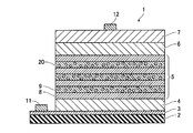
- FIG. 2 is a partial cross-sectional view of the infrared sensor of the present embodiment.
- the infrared sensor 1 includes, in order from the bottom, a semi-insulating substrate 2, a first electrode forming layer 3, a first spacer layer 4, a light absorbing layer 5, and a second spacer layer 6. And a second electrode forming layer 7.
- the light absorption layer 5 has a structure in which the intermediate layers 8 and the quantum dot layers 9 are alternately stacked.
- a plurality of quantum dot layers 9 are formed.
- one quantum dot layer 9 may be provided.
- the intermediate layer 8 has a wider band gap than the quantum dots 20 included in the quantum dot layer 9.
- the upper and lower portions of the quantum dot layer 9 are sandwiched between the intermediate layers 8.
- Al y Ga 1-y As (0 ⁇ y ⁇ 1) can be used.
- Al z Ga 1-z As (0 ⁇ y ⁇ 1) can be used.
- the intermediate layer 8 and the spacer layers 4 and 6 are made of the same material, the adjacent intermediate layer 8 and spacer layers 4 and 6 may be formed as a single layer instead of having a two-layer structure.
- the semi-insulating substrate 2 for example, a semi-insulating GaAs substrate can be used.
- the first electrode forming layer 3 of n-type GaAs can be formed on the surface of the semi-insulating GaAs substrate by doping, for example, Si.
- an emitter electrode 11 is provided on the surface of the first electrode forming layer 3
- a collector electrode 12 is provided on the surface of the second electrode forming layer 7.
- a voltage is applied to the light absorbing layer 5 by a power supply (not shown) via the emitter electrode 11 and the collector electrode 12.
- the emitter electrode 11 becomes higher in energy than the collector electrode 12. Thereby, a gradient electric field is formed in the light absorption layer 5.
- the infrared ray is incident on the light absorption layer 5, the electrons bound to the quantum level on the conduction band side of the quantum dot are excited and escape. The escaped electrons move to the collector electrode 12 by the electric field and form a photocurrent.
- a plurality of spherical quantum dots 20 are dispersedly arranged in the quantum dot layer 9.
- the term “spherical” is not limited to a true sphere, but a sphericity of 0.7 or more, preferably 0.8 or more, more preferably 0.9 or more. Point to.
- the sphericity can be measured by performing image processing with an electron microscope and calculating the sphericity by using 4 ⁇ ⁇ (area) ⁇ (perimeter) 2 from the observed area and perimeter of the quantum dot. it can.
- the observed aspect ratio of the quantum dot expressed by the major axis / minor axis is 1.5 or less, preferably 1.2 or less, more preferably 1.3 or less, it is defined as “spherical”. You.
- the quantum dots 20 can be formed by liquid phase synthesis.
- the quantum dot 20 of the present embodiment is preferably spherical as described above, but is not limited to this.
- the quantum dots 20 synthesized by the liquid phase synthesis method may be formed in the above-described spherical shape or in a shape other than the spherical shape. Examples of the shape other than the spherical shape include a rod shape and a tree shape.
- a resin composition in which a plurality of spherical quantum dots 20 are dispersed in a resin can be formed by alternately applying the resin composition to the intermediate layer 8.
- the dispersion resin for the quantum dots 20 is not particularly limited, but polypropylene, polyethylene, polystyrene, AS resin, ABS resin, methacrylic resin, polyvinyl chloride, polyacetal, polyamide, polycarbonate, modified polyphenylene ether, polybutylene terephthalate, Polyethylene terephthalate, polysulfone, polyethersulfone, polyphenylene sulfide, polyamideimide, polymethylpentene, liquid crystal polymer, epoxy resin, phenol resin, urea resin, melamine resin, epoxy resin, diallyl phthalate resin, unsaturated polyester resin, polyimide, polyurethane , Silicone resin, cyclic polyolefin polymer (Cyclic Olefin Polymer: COP), cyclic polyolefin polymer (
- a plurality of spherical quantum dots 20 can be applied by using an inkjet method in a state of being dissolved in a solvent.
- the dried quantum dot layer 9 is composed of substantially spherical quantum dots 20, but some solvent components may be left in the quantum dot layer 9.
- the quantum dots 20 have an emission wavelength between about 800 nm and 1600 nm.
- the quantum dot 20 having such an emission wavelength at least one of PbS, PbSe, CdHgTe, Ag 2 S, Ag 2 Se, Ag 2 Te, AgInSe 2 , AgInTe 2 , CuInSe 2 , CuInTe 2 , and InAs It is preferable to include one kind. Among them, Ag 2 S does not correspond to the RoHS command.
- PbS was published in 2003 WILEY-VCH Verlag GmbH & Co. KGaA. Weinheim. ADVANCED MATERIALS 2003, 15.NO.21 November 4. Ag 2 S has been published in ACS NANO VOL.6 NO.5 P3695-3702 (2012).
- PbS or Ag 2 S for the quantum dots 20.
- Ag 2 S, Ag 2 Se, Ag 2 Te, AgInSe 2 , or AgInTe 2 for the quantum dots 20.
- the fluorescence half width in the near-infrared region can be narrowed, and high-intensity near-infrared light can be obtained. It can show fluorescence.
- the plurality of quantum dots 20 may be one type or two or more types. That is, all of the plurality of quantum dots 20 may be of the same type or may be of different types.
- the quantum dots 20 in the present embodiment are, for example, nanoparticles having a particle size of about several nm to several tens nm.
- ligands 21 are coordinated on the surface of the quantum dot 20. Thereby, aggregation of the quantum dots 20 can be suppressed, and a desired optical characteristic is exhibited.
- the ligands that can be used in the reaction are not particularly limited, and for example, the following ligands are exemplified.
- a short ligand (ligand)
- MPA 3-mercaptopropionic acid
- the ligand of the quantum dot 20 included in the quantum dot layer 9 is shorter than the ligand when the quantum dot 20 is formed by the liquid phase synthesis method.
- the roughness of the quantum dot layer 9 can be reduced, and the efficiency of taking out electrons and holes can be improved.
- a long ligand for forming the quantum dots 20 by the liquid phase synthesis method it is possible to improve the dispersion film forming property.
- a short ligand for example, 3-mercaptopropionic acid
- a composition containing the quantum dot 20 is replaced by
- the quantum dot 20 may have a core-shell structure including a core 20a and a shell 20b coated on the surface of the core 20a. As shown in FIG. 4B, it is preferable that a large number of organic ligands 21 are coordinated on the surface of the quantum dot 20.
- the organic ligand 21 is as described above.
- the core 20a of the quantum dot 20 shown in FIG. 4B is the nanoparticle shown in FIG. 3A. Therefore, the core 20a is formed of, for example, the material of the quantum dots 20 described above.
- the shell 20b may be in a solid solution state on the surface of the core 20a.
- the boundary between the core 20a and the shell 20b is indicated by a dotted line, which indicates that the boundary between the core 20a and the shell 20b can be confirmed by analysis or not.
- the infrared sensor 1 shown in FIG. 2 is inverted to form an infrared sensor (QDIP array) 101 with the semi-insulating substrate 2 facing upward, and this infrared sensor 101 is mounted on a circuit board 102 via bumps 104 shown in FIG. Electrically connected to
- FIG. 5 is a partial cross-sectional view of the infrared sensor of the present embodiment, which is partially different from FIG.
- the infrared sensor shown in FIG. 5 has a laminated structure including, in order from the bottom, a semi-insulating substrate 2, a first electrode forming layer 3, a light absorbing layer 15, and a second electrode forming layer 7.
- the light absorbing layer 15 is formed in a laminated structure of the intermediate layer 18 / the barrier layer 30 / the quantum dot layer 19 / the barrier layer 30 / the intermediate layer 18.
- the potential of the barrier layer 30 for carriers is higher than the potential of the intermediate layer 18 for carriers. Further, the potential of the quantum dots 20 included in the quantum dot layer 19 with respect to the carriers is lower than the potential of the intermediate layer 18 with respect to the carriers. Further, the potential of the quantum dots 20 with respect to the carriers is lower than the potential of the barrier layers 30 with respect to the carriers.
- the band gap of the barrier layer 30 is larger than the band gap of the intermediate layer 18. The band gap of the quantum dot 20 is smaller than each band gap of the intermediate layer 18 and the barrier layer 30.
- the quantum dots 20 included in the light absorption layer 15 of the infrared sensor shown in FIG. 5 are spherical. Moreover, the quantum dots 20, PbS, PbSe, CdHgTe, Ag 2 S, Ag 2 Se, Ag 2 Te, AgInSe 2, AgInTe 2, CuInSe 2, CuInTe 2, of InAs, include at least one kind preferable.
- the infrared sensor shown in FIG. 5 is inverted to form an infrared sensor (QDIP array) 101 with the semi-insulating substrate 2 side facing upward, and this infrared sensor 101 is connected via bumps 104 shown in FIG. And electrically connected to the circuit board 102.
- the stacked structure shown in FIGS. 2 and 5 may be formed separately for each pixel.
- a far-infrared region for detecting far-infrared light for example, a mid-infrared region for detecting mid-infrared light, and near-infrared light are detected. It can be divided into two or more regions in the near infrared region.
- the long wavelength region is arranged on the light receiving surface side, that is, on the semi-insulating substrate 2 side.
- a quantum dot layer including a quantum dot having an emission wavelength in the mid-infrared region is formed in a quantum dot layer in the mid-infrared region, and a quantum dot layer having an emission wavelength in the near-infrared region is formed in the quantum dot layer in the near-infrared region.
- a quantum dot layer including dots is formed.
- FIG. 6 is a partially enlarged cross-sectional view of an infrared imaging device including the infrared sensor of the present embodiment.
- the infrared sensor 101 has an infrared detection layer 120 for detecting infrared light and a visible light detection layer 121 for detecting visible light.
- the configuration of the infrared detecting layer 120 shown in FIG. 6 is the laminated structure shown in FIGS. 2 and 5, the quantum dots used are spherical, and PbS, PbSe, CdHgTe, Ag 2 S, Ag 2 Se are used. , Ag 2 Te, AgInSe 2, AgInTe 2, CuInSe 2, CuInTe 2, of the InAs, preferably contains at least one kind.
- quantum dots having an emission wavelength in the visible light range are applied to the quantum dots applied to the visible light detection layer 121.
- the structure and material of the quantum dot are not limited, but, for example, the quantum dot in the present embodiment is a nanoparticle having a particle size of about several nm to several tens nm.
- the quantum dots applied to the visible light region are formed of, for example, CdS, CdSe, ZnS, ZnSe, ZnSeS, ZnTe, ZnTeS, InP, chalcopyrite (CuInS, AgInS), and the like. Is done.
- the structure of the quantum dots used in the visible light detecting layer 121 may be the single core structure shown in FIG. 4A or the core-shell structure shown in FIG. 4B.
- the installation location of the cooling device 130 is not limited as long as the quantum dot layer can be cooled appropriately.
- the infrared sensor having the quantum dots of the present embodiment can strongly confine carriers, has excellent sensitivity to vertically incident light, and is expected to be a highly sensitive and low dark current infrared detector. I have.
- the quantum dot layer is finely processed into an island shape. For this reason, fine processing adjustment is required, and the manufacturing process is likely to be complicated. Also, the manufacturing cost is likely to increase.
- the spherical quantum dots are applied, and there is no need for fine processing unlike the related art, and the conventional problem does not occur.
- quantum dots particularly spherical quantum dots formed by a liquid phase synthesis method are used, the sensitivity is excellent in all directions, and the sensitivity is higher than that of a conventional microfabricated quantum dot. Variation can be reduced.
- PbS, PbSe, CdHgTe, Ag 2 S, Ag 2 Se, Ag 2 Te, AgInSe 2, AgInTe 2, CuInSe 2, CuInTe 2, of the InAs at least one kind It is preferable to include These have an emission wavelength of 800 nm to 1600 nm and can be preferably applied to an infrared sensor.
- the infrared sensor according to the present embodiment can be applied to, for example, a photoelectric device or a thermoelectric device described below.
- FIGS. 7 and 8 are partial cross-sectional views showing an example of the photoelectric conversion element of the present embodiment.
- 7 includes a first conductive layer 41 serving as a cathode and a second conductive layer 42 serving as an anode.
- An electron transporting layer 43 is provided between the first conductive layer 41 and the second conductive layer 42.
- a light absorbing layer 44 and a hole transport layer 45 are provided.
- the first conductive layer 41 is formed on a glass substrate 46.
- the light absorption layer 44 is a layer that absorbs light incident on the photoelectric conversion element 40 and generates electrons and holes, and includes the above-described spherical quantum dots.
- the photoelectric conversion element (PN-type photodiode) 50 illustrated in FIG. 8 includes a P-type semiconductor layer 53 and an N-type semiconductor layer 54 between a first electrode 51 and a second electrode 52.
- the structure is a structure in which the electrodes 51 and 52 are arranged on a PN-junction semiconductor, and is the same as a solar cell.
- the n-type semiconductor has many mobile electrons, and some of the electrons move to the p-type semiconductor and combine with holes to cancel charges, thereby forming a region called a depletion layer.
- the n-type semiconductor in the depletion layer is charged positively, and the p-type semiconductor is negatively charged because there are no holes, and an internal electric field is generated.
- the infrared sensor can be applied to an imaging device, a medical field, a communication field, a solar cell, and the like.
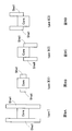
- the energy level diagram becomes any one of FIGS. 9A to 9D.
- a shell having a core-shell structure is important in terms of improving the quantum confinement effect.
- the type @ I structure (the LUMO of the shell has higher energy than the LUMO of the core, and the energy of the HOMO of the shell is lower than that of the core) shown in FIG. 9A is preferable.
- a type II structure when used for a photoelectric conversion element, a type II structure is preferable so that carriers (electrons and holes) can be easily extracted. Since the hole mobility is usually lower than the electron mobility, the type II (1) or , (3) are preferably selected.
- a quantum dot having a core structure having a ligand instead of a core-shell structure can be used.
- the LUMO of the shell has lower energy than the LUMO of the core, and the HOMO of the shell has higher energy than the HOMO of the core.
- type @ II (3) the LUMO of the shell has higher energy than the LUMO of the core, and the HOMO of the shell has higher energy than the HOMO of the core.
- a step of forming spherical quantum dots by a liquid phase synthesis method and a step of forming a light absorbing layer by applying a resin composition containing a plurality of quantum dots are included. , Including.
- each element source constituting a quantum dot is dissolved in a solvent, a precursor solution having each element is reacted using, for example, a microreactor, and a predetermined element is provided.
- Quantum dot particles can be synthesized. Thereby, spherical quantum dots can be obtained.
- the quantum dot has a long-chain ligand.
- a short-chain ligand is used in order to increase the efficiency of taking out carriers (electrons and holes). It is preferred that although not limited, the carbon number of the short-chain ligand is 2 to 5 (preferably 2 to 3).
- the short-chain ligand for example, 3-mercaptopropionic acid is used. Can be.
- the ligands of the quantum dots can be replaced with short ligands.
- a composition containing quantum dots including quantum dots and a solvent
- a long-chain ligand has better dispersibility, so that a film with good roughness can be formed.However, with a long-chain ligand, removal of carriers is disadvantageous. Drop the ligand over the coating. This naturally replaces the long-chain ligand with the short-chain ligand, followed by washing to wash away the long-chain ligand.
- a quantum dot is synthesized by a liquid phase synthesis method
- a long-chain ligand is replaced with a short-chain ligand before coating, and then a composition containing a quantum dot (even a resin composition). (Good).
- infrared rays can be detected.
- the infrared sensor of the present invention can be applied to night vision devices, heat source detection devices, security devices, medical equipment, and the like.
Landscapes
- Physics & Mathematics (AREA)
- General Physics & Mathematics (AREA)
- Spectroscopy & Molecular Physics (AREA)
- Light Receiving Elements (AREA)
- Photometry And Measurement Of Optical Pulse Characteristics (AREA)
- Chemical & Material Sciences (AREA)
- Engineering & Computer Science (AREA)
- Nanotechnology (AREA)
- Encapsulation Of And Coatings For Semiconductor Or Solid State Devices (AREA)
Abstract
Description
に関する。
オレイルアミン:C18H35NH2、ステアリル(オクタデシル)アミン:C18H37NH2、ドデシル(ラウリル)アミン:C12H25NH2、デシルアミン:C10H21NH2、オクチルアミン:C8H17NH2
(2)脂肪酸系
オレイン酸:C17H33COOH、ステアリン酸:C17H35COOH、パルミチン酸:C15H31COOH、ミリスチン酸:C13H27COOH、ラウリル酸:C11H23COOH、デカン酸:C9H19COOH、オクタン酸:C7H15COOH
(3)チオール系
オクタデカンチオール:C18H37SH、ヘキサンデカンチオール:C16H33SH、テトラデカンチオール:C14H29SH、ドデカンチオール:C12H25SH、デカンチオール:C10H21SH、オクタンチオール:C8H17SH
(4)ホスフィン系
トリオクチルホスフィン:(C8H17)3P、トリフェニルホスフィン:(C6H5)3P、トリブチルホスフィン:(C4H9)3P
(5)ホスフィンオキシド系
トリオクチルホスフィンオキシド:(C8H17)3P=O、トリフェニルホスフィンオキシド:(C6H5)3P=O、トリブチルホスフィンオキシド:(C4H9)3P=O
図2及び図5に示す積層構造は、画素ごとに分割して形成されていてもよい。
Claims (9)
- 赤外線を吸収する光吸収層を具備した赤外線センサであって、
前記光吸収層は、複数の量子ドットを含み、
前記量子ドットは、球状である、
ことを特徴とする赤外線センサ。 - 赤外線を吸収する光吸収層を具備した赤外線センサであって、
前記光吸収層は、複数の量子ドットを含み、
前記量子ドットは、PbS、PbSe、CdHgTe、Ag2S、Ag2Se、Ag2Te、AgInSe2、AgInTe2、CuInSe2、CuInTe2、InAsのうち、少なくともいずれか1種を含む、
ことを特徴とする赤外線センサ。 - 赤外線を吸収する光吸収層を具備した赤外線センサであって、
前記光吸収層は、複数の量子ドットを含み、
前記量子ドットは、液相合成により形成されたものであることを特徴とする赤外線センサ。 - 前記量子ドットは、球状であることを特徴とする請求項2又は請求項3に記載の赤外線センサ。
- 前記量子ドットを含む量子ドット層を、塗布して形成したことを特徴とする請求項1から請求項4のいずれかに記載の赤外線センサ。
- 前記光吸収層に含まれる前記量子ドットの配位子は、前記液相合成で形成された際の前記量子ドットの前記配位子よりも短いことを特徴とする請求項1から請求項5のいずれかに記載の赤外線センサ。
- 前記赤外線センサは、光電素子或いは、熱電素子を含むことを特徴とする請求項1から請求項6に記載の赤外線センサ。
- 赤外線を吸収する光吸収層を具備した赤外線センサの製造方法であって、
量子ドットを、液相合成法により形成する工程、
複数の前記量子ドットを含む組成物を塗布して、前記光吸収層を形成する工程、を有することを特徴とする赤外線センサの製造方法。 - 前記液相合成法により量子ドットを合成した後、前記量子ドットの配位子を、短い配位子に置き換えることを特徴とする請求項8に記載の赤外線センサの製造方法。
Priority Applications (7)
| Application Number | Priority Date | Filing Date | Title |
|---|---|---|---|
| CN201980059015.6A CN112703609A (zh) | 2018-09-12 | 2019-09-11 | 红外线传感器及其制造方法 |
| KR1020247038294A KR20240166045A (ko) | 2018-09-12 | 2019-09-11 | 적외선 센서 및 그 제조 방법 |
| US17/273,895 US12266734B2 (en) | 2018-09-12 | 2019-09-11 | Infrared sensor and manufacturing method for the same |
| KR1020217006900A KR102732888B1 (ko) | 2018-09-12 | 2019-09-11 | 적외선 센서 및 그 제조 방법 |
| JP2020546054A JPWO2020054764A1 (ja) | 2018-09-12 | 2019-09-11 | 赤外線センサ及びその製造方法 |
| EP19859093.7A EP3852151A4 (en) | 2018-09-12 | 2019-09-11 | INFRARED SENSOR AND METHOD OF MANUFACTURE THEREOF |
| US19/053,398 US20250185386A1 (en) | 2018-09-12 | 2025-02-13 | Infrared sensor and manufacturing method for the same |
Applications Claiming Priority (2)
| Application Number | Priority Date | Filing Date | Title |
|---|---|---|---|
| JP2018170491 | 2018-09-12 | ||
| JP2018-170491 | 2018-09-12 |
Related Child Applications (2)
| Application Number | Title | Priority Date | Filing Date |
|---|---|---|---|
| US17/273,895 A-371-Of-International US12266734B2 (en) | 2018-09-12 | 2019-09-11 | Infrared sensor and manufacturing method for the same |
| US19/053,398 Continuation US20250185386A1 (en) | 2018-09-12 | 2025-02-13 | Infrared sensor and manufacturing method for the same |
Publications (1)
| Publication Number | Publication Date |
|---|---|
| WO2020054764A1 true WO2020054764A1 (ja) | 2020-03-19 |
Family
ID=69778412
Family Applications (1)
| Application Number | Title | Priority Date | Filing Date |
|---|---|---|---|
| PCT/JP2019/035713 Ceased WO2020054764A1 (ja) | 2018-09-12 | 2019-09-11 | 赤外線センサ及びその製造方法 |
Country Status (7)
| Country | Link |
|---|---|
| US (2) | US12266734B2 (ja) |
| EP (1) | EP3852151A4 (ja) |
| JP (1) | JPWO2020054764A1 (ja) |
| KR (2) | KR20240166045A (ja) |
| CN (1) | CN112703609A (ja) |
| TW (2) | TWI902020B (ja) |
| WO (1) | WO2020054764A1 (ja) |
Cited By (8)
| Publication number | Priority date | Publication date | Assignee | Title |
|---|---|---|---|---|
| JPWO2022149516A1 (ja) * | 2021-01-06 | 2022-07-14 | ||
| WO2022208641A1 (ja) * | 2021-03-30 | 2022-10-06 | シャープ株式会社 | 発光素子、表示デバイス、発光素子の製造方法、表示デバイスの製造方法 |
| WO2023008353A1 (ja) * | 2021-07-29 | 2023-02-02 | 富士フイルム株式会社 | 光検出素子およびイメージセンサ |
| WO2023149392A1 (ja) | 2022-02-03 | 2023-08-10 | 国立大学法人東海国立大学機構 | AgAuS系多元化合物からなる半導体ナノ粒子 |
| WO2024157922A1 (ja) | 2023-01-26 | 2024-08-02 | 国立大学法人東海国立大学機構 | AgAuSe系多元化合物からなる半導体ナノ粒子 |
| WO2025094866A1 (ja) | 2023-10-31 | 2025-05-08 | 国立大学法人東海国立大学機構 | AgAuTe化合物を主成分とする半導体ナノ粒子 |
| WO2025127101A1 (ja) * | 2023-12-15 | 2025-06-19 | Toppanホールディングス株式会社 | 太陽電池、ナノ材料、及び分散液、並びに太陽電池の製造方法 |
| WO2026063231A1 (ja) * | 2024-09-20 | 2026-03-26 | 富士フイルム株式会社 | 量子ドット分散液、半導体膜、半導体膜の製造方法、光検出素子およびイメージセンサ |
Families Citing this family (5)
| Publication number | Priority date | Publication date | Assignee | Title |
|---|---|---|---|---|
| US20230082643A1 (en) * | 2021-09-13 | 2023-03-16 | Lawrence Livermore National Security, Llc | Surface treatment for colloidal stability of in-solution ligand exchanged quantum dots |
| KR102689038B1 (ko) * | 2022-10-20 | 2024-07-29 | 국방과학연구소 | 초균일 양자점 박막을 통한 중파장 적외선 초고감도 광검출기 개발 |
| KR102686198B1 (ko) | 2022-10-26 | 2024-07-17 | 고려대학교 산학협력단 | 황화납 양자점 포토다이오드와 그 제조방법 및 응용 제품 |
| KR20250118077A (ko) * | 2024-01-29 | 2025-08-05 | 고려대학교 산학협력단 | 비독성 귀금속 칼코게나이드 양자점 나노결정 기반 적외선 광학 장치 및 이의 제조방법 |
| CN121510684B (zh) * | 2026-01-14 | 2026-04-21 | 中北大学 | 一种异质结构的光热电探测器及其制备方法 |
Citations (14)
| Publication number | Priority date | Publication date | Assignee | Title |
|---|---|---|---|---|
| US20100309460A1 (en) * | 2009-06-03 | 2010-12-09 | Sargent Edward H | Photoconductive materials and devices with internal photoconductive gain |
| JP2013089969A (ja) * | 2011-10-18 | 2013-05-13 | Samsung Electronics Co Ltd | 無機リガンドを有する量子ドット及びその製造方法 |
| JP2014093327A (ja) * | 2012-10-31 | 2014-05-19 | Fujifilm Corp | 半導体膜、半導体膜の製造方法、太陽電池、発光ダイオード、薄膜トランジスタ、および、電子デバイス |
| JP2015505860A (ja) * | 2011-10-20 | 2015-02-26 | コーニンクレッカ フィリップス エヌ ヴェ | 量子ドットを有する光源 |
| JP2015141970A (ja) * | 2014-01-28 | 2015-08-03 | シャープ株式会社 | 受光素子および受光素子を備えた太陽電池 |
| JP2015162478A (ja) | 2014-02-26 | 2015-09-07 | 防衛省技術研究本部長 | 量子ドット型赤外線検知素子、量子ドット型赤外線検知器及び量子ドット型赤外線撮像装置 |
| JP2015189636A (ja) * | 2014-03-28 | 2015-11-02 | 国立大学法人名古屋大学 | テルル化合物ナノ粒子及びその製法 |
| US20160172513A1 (en) * | 2014-12-11 | 2016-06-16 | Vadient Optics, LLC. | Composite quantum-dot materials for photonics detectors |
| JP2016532301A (ja) * | 2013-08-29 | 2016-10-13 | ユニバーシティー オブ フロリダ リサーチ ファウンデーション,インコーポレイテッドUniversity Of Florida Research Foundation,Inc. | 溶液から作製された無機半導体から空気中で安定な赤外線光検出器 |
| WO2017061174A1 (ja) * | 2015-10-09 | 2017-04-13 | ソニー株式会社 | 光電変換素子および撮像素子 |
| JP2018006363A (ja) * | 2016-06-27 | 2018-01-11 | シャープ株式会社 | 光電変換素子およびそれを備えた光電変換装置 |
| WO2018016213A1 (ja) * | 2016-07-20 | 2018-01-25 | ソニー株式会社 | 半導体膜及びその製造方法、並びに、光電変換素子、固体撮像素子及び電子装置 |
| JP2018107465A (ja) * | 2016-08-04 | 2018-07-05 | 花王株式会社 | 光吸収層、光電変換素子、及び太陽電池 |
| JP2018170491A (ja) | 2016-11-29 | 2018-11-01 | パロ アルト リサーチ センター インコーポレイテッド | 薄膜および基板除去iii族窒化物ベースのデバイスおよび方法 |
Family Cites Families (24)
| Publication number | Priority date | Publication date | Assignee | Title |
|---|---|---|---|---|
| EP0853334B1 (en) * | 1996-06-19 | 2006-07-05 | Matsushita Electric Industrial Co., Ltd. | Optoelectronic material, devices using the same, and method for manufacturing the same |
| US6452242B1 (en) * | 2000-03-23 | 2002-09-17 | Mp Technologies Llc | Multi color detector |
| US6727521B2 (en) * | 2000-09-25 | 2004-04-27 | Foveon, Inc. | Vertical color filter detector group and array |
| US7326908B2 (en) | 2004-04-19 | 2008-02-05 | Edward Sargent | Optically-regulated optical emission using colloidal quantum dot nanocrystals |
| EP1667246A1 (en) * | 2004-12-03 | 2006-06-07 | ETeCH AG | A multi-colour sensitive device for colour image sensing |
| US7923801B2 (en) * | 2007-04-18 | 2011-04-12 | Invisage Technologies, Inc. | Materials, systems and methods for optoelectronic devices |
| JP4842291B2 (ja) * | 2008-03-19 | 2011-12-21 | 富士通株式会社 | 光半導体装置及び赤外線検出装置 |
| CN101519696B (zh) * | 2009-02-19 | 2011-09-14 | 中国人民解放军第三军医大学第一附属医院 | 基于量子点的核酸传感器及其制备方法和检测方法 |
| DK2483925T3 (en) | 2009-09-29 | 2018-08-20 | Res Triangle Inst | QUANTITY POINT FILLER TRANSITION BASED PHOTO DETECTORS |
| WO2011047198A1 (en) * | 2009-10-14 | 2011-04-21 | The Regents Of The University Of California | Nanocomposite and method of making thereof |
| US9382474B2 (en) | 2010-04-06 | 2016-07-05 | The Governing Council Of The University Of Toronto | Photovoltaic devices with depleted heterojunctions and shell-passivated nanoparticles |
| US8975509B2 (en) * | 2010-06-07 | 2015-03-10 | The Governing Council Of The University Of Toronto | Photovoltaic devices with multiple junctions separated by a graded recombination layer |
| JP5302270B2 (ja) * | 2010-07-08 | 2013-10-02 | 防衛省技術研究本部長 | 量子ドット型赤外線検知素子及び量子ドット型赤外線撮像装置 |
| WO2012018649A2 (en) * | 2010-08-06 | 2012-02-09 | Spectrawatt, Inc. | Cooperative photovoltaic networks and photovoltaic cell adaptations for use therein |
| US9196760B2 (en) * | 2011-04-08 | 2015-11-24 | Ut-Battelle, Llc | Methods for producing complex films, and films produced thereby |
| US8779413B1 (en) * | 2012-10-09 | 2014-07-15 | Sunpower Technologies Llc | Optoelectronic devices with all-inorganic colloidal nanostructured films |
| CA2899045A1 (en) * | 2013-02-21 | 2014-08-28 | The Governing Council Of The University Of Toronto | Photovoltaic devices with plasmonic nanoparticles |
| JP2015128105A (ja) | 2013-12-27 | 2015-07-09 | ソニー株式会社 | 半導体ナノ粒子分散体、光電変換素子および撮像装置 |
| CA2948486A1 (en) | 2014-05-09 | 2015-11-12 | Massachusetts Institute Of Technology | Energy level modification of nanocrystals through ligand exchange |
| AU2015365738B2 (en) * | 2014-12-19 | 2020-07-23 | Galderma Research & Development | Novel compounds, synthesis method thereof and use of same in medicine and in cosmetics |
| CA2988784A1 (en) | 2015-06-11 | 2017-03-09 | University Of Florida Research Foundation, Incorporated | Monodisperse, ir-absorbing nanoparticles and related methods and devices |
| KR102053086B1 (ko) * | 2016-07-15 | 2019-12-06 | 주식회사 엘지화학 | 양자점을 이용한 광변환소자 |
| CN115275032B (zh) * | 2016-12-28 | 2025-12-23 | 株式会社半导体能源研究所 | 发光元件、有机化合物、发光装置、电子设备及照明装置 |
| JP7204667B2 (ja) * | 2017-04-20 | 2023-01-16 | トリナミクス ゲゼルシャフト ミット ベシュレンクテル ハフツング | 光検出器 |
-
2019
- 2019-09-11 EP EP19859093.7A patent/EP3852151A4/en active Pending
- 2019-09-11 KR KR1020247038294A patent/KR20240166045A/ko active Pending
- 2019-09-11 KR KR1020217006900A patent/KR102732888B1/ko active Active
- 2019-09-11 CN CN201980059015.6A patent/CN112703609A/zh active Pending
- 2019-09-11 WO PCT/JP2019/035713 patent/WO2020054764A1/ja not_active Ceased
- 2019-09-11 US US17/273,895 patent/US12266734B2/en active Active
- 2019-09-11 JP JP2020546054A patent/JPWO2020054764A1/ja active Pending
- 2019-09-12 TW TW112137014A patent/TWI902020B/zh active
- 2019-09-12 TW TW108132953A patent/TWI819092B/zh active
-
2025
- 2025-02-13 US US19/053,398 patent/US20250185386A1/en active Pending
Patent Citations (14)
| Publication number | Priority date | Publication date | Assignee | Title |
|---|---|---|---|---|
| US20100309460A1 (en) * | 2009-06-03 | 2010-12-09 | Sargent Edward H | Photoconductive materials and devices with internal photoconductive gain |
| JP2013089969A (ja) * | 2011-10-18 | 2013-05-13 | Samsung Electronics Co Ltd | 無機リガンドを有する量子ドット及びその製造方法 |
| JP2015505860A (ja) * | 2011-10-20 | 2015-02-26 | コーニンクレッカ フィリップス エヌ ヴェ | 量子ドットを有する光源 |
| JP2014093327A (ja) * | 2012-10-31 | 2014-05-19 | Fujifilm Corp | 半導体膜、半導体膜の製造方法、太陽電池、発光ダイオード、薄膜トランジスタ、および、電子デバイス |
| JP2016532301A (ja) * | 2013-08-29 | 2016-10-13 | ユニバーシティー オブ フロリダ リサーチ ファウンデーション,インコーポレイテッドUniversity Of Florida Research Foundation,Inc. | 溶液から作製された無機半導体から空気中で安定な赤外線光検出器 |
| JP2015141970A (ja) * | 2014-01-28 | 2015-08-03 | シャープ株式会社 | 受光素子および受光素子を備えた太陽電池 |
| JP2015162478A (ja) | 2014-02-26 | 2015-09-07 | 防衛省技術研究本部長 | 量子ドット型赤外線検知素子、量子ドット型赤外線検知器及び量子ドット型赤外線撮像装置 |
| JP2015189636A (ja) * | 2014-03-28 | 2015-11-02 | 国立大学法人名古屋大学 | テルル化合物ナノ粒子及びその製法 |
| US20160172513A1 (en) * | 2014-12-11 | 2016-06-16 | Vadient Optics, LLC. | Composite quantum-dot materials for photonics detectors |
| WO2017061174A1 (ja) * | 2015-10-09 | 2017-04-13 | ソニー株式会社 | 光電変換素子および撮像素子 |
| JP2018006363A (ja) * | 2016-06-27 | 2018-01-11 | シャープ株式会社 | 光電変換素子およびそれを備えた光電変換装置 |
| WO2018016213A1 (ja) * | 2016-07-20 | 2018-01-25 | ソニー株式会社 | 半導体膜及びその製造方法、並びに、光電変換素子、固体撮像素子及び電子装置 |
| JP2018107465A (ja) * | 2016-08-04 | 2018-07-05 | 花王株式会社 | 光吸収層、光電変換素子、及び太陽電池 |
| JP2018170491A (ja) | 2016-11-29 | 2018-11-01 | パロ アルト リサーチ センター インコーポレイテッド | 薄膜および基板除去iii族窒化物ベースのデバイスおよび方法 |
Non-Patent Citations (3)
| Title |
|---|
| "ADVANCED MATERIALS", vol. 15, 4 November 2003, WILEY-VCH VERLAG GMBH CO. KGAA, pages: 21 |
| ACS NANO, vol. 6, no. 5, 2012, pages 3695 - 3702 |
| See also references of EP3852151A4 |
Cited By (16)
| Publication number | Priority date | Publication date | Assignee | Title |
|---|---|---|---|---|
| JPWO2022149516A1 (ja) * | 2021-01-06 | 2022-07-14 | ||
| WO2022149516A1 (ja) * | 2021-01-06 | 2022-07-14 | 田中貴金属工業株式会社 | 光電変換素子材料及び光電変換素子材料の製造方法並びに半導体ナノ粒子が分散されたインク |
| JP7621387B2 (ja) | 2021-01-06 | 2025-01-24 | 田中貴金属工業株式会社 | 光電変換素子材料及び光電変換素子材料の製造方法並びに半導体ナノ粒子が分散されたインク |
| WO2022208641A1 (ja) * | 2021-03-30 | 2022-10-06 | シャープ株式会社 | 発光素子、表示デバイス、発光素子の製造方法、表示デバイスの製造方法 |
| WO2022208917A1 (ja) * | 2021-03-30 | 2022-10-06 | シャープ株式会社 | 発光素子、表示デバイス、発光素子の製造方法、表示デバイスの製造方法、量子ドットコロイド溶液の製造方法、及び、量子ドットコロイド溶液 |
| WO2023008353A1 (ja) * | 2021-07-29 | 2023-02-02 | 富士フイルム株式会社 | 光検出素子およびイメージセンサ |
| JPWO2023008353A1 (ja) * | 2021-07-29 | 2023-02-02 | ||
| KR20240137668A (ko) | 2022-02-03 | 2024-09-20 | 고쿠리츠 다이가쿠 호우징 도우카이 고쿠리츠 다이가쿠 기코우 | AgAuS계 다원 화합물로 이루어지는 반도체 나노 입자 |
| WO2023149392A1 (ja) | 2022-02-03 | 2023-08-10 | 国立大学法人東海国立大学機構 | AgAuS系多元化合物からなる半導体ナノ粒子 |
| US12441938B2 (en) | 2022-02-03 | 2025-10-14 | National University Corporation Tokai National Higher Education And Research System | Semiconductor nanoparticles composed of AgAuS-based multicomponent compound |
| WO2024157922A1 (ja) | 2023-01-26 | 2024-08-02 | 国立大学法人東海国立大学機構 | AgAuSe系多元化合物からなる半導体ナノ粒子 |
| KR20250133370A (ko) | 2023-01-26 | 2025-09-05 | 고쿠리츠 다이가쿠 호우징 도우카이 고쿠리츠 다이가쿠 기코우 | AgAuSe계 다원 화합물로 이루어지는 반도체 나노입자 |
| EP4656595A1 (en) | 2023-01-26 | 2025-12-03 | National University Corporation Tokai National Higher Education And Research System | Semiconductor nanoparticles composed of agause-based multinary compound |
| WO2025094866A1 (ja) | 2023-10-31 | 2025-05-08 | 国立大学法人東海国立大学機構 | AgAuTe化合物を主成分とする半導体ナノ粒子 |
| WO2025127101A1 (ja) * | 2023-12-15 | 2025-06-19 | Toppanホールディングス株式会社 | 太陽電池、ナノ材料、及び分散液、並びに太陽電池の製造方法 |
| WO2026063231A1 (ja) * | 2024-09-20 | 2026-03-26 | 富士フイルム株式会社 | 量子ドット分散液、半導体膜、半導体膜の製造方法、光検出素子およびイメージセンサ |
Also Published As
| Publication number | Publication date |
|---|---|
| EP3852151A4 (en) | 2022-06-15 |
| KR20240166045A (ko) | 2024-11-25 |
| TW202019810A (zh) | 2020-06-01 |
| TWI819092B (zh) | 2023-10-21 |
| KR102732888B1 (ko) | 2024-11-25 |
| TWI902020B (zh) | 2025-10-21 |
| US20210234056A1 (en) | 2021-07-29 |
| KR20210049113A (ko) | 2021-05-04 |
| JPWO2020054764A1 (ja) | 2021-08-30 |
| US12266734B2 (en) | 2025-04-01 |
| TW202402657A (zh) | 2024-01-16 |
| CN112703609A (zh) | 2021-04-23 |
| US20250185386A1 (en) | 2025-06-05 |
| EP3852151A1 (en) | 2021-07-21 |
Similar Documents
| Publication | Publication Date | Title |
|---|---|---|
| KR102732888B1 (ko) | 적외선 센서 및 그 제조 방법 | |
| KR101596972B1 (ko) | 유형 ⅱ 양자점 태양전지 | |
| EP2483925B1 (en) | Quantum dot-fullerene junction based photodetectors | |
| US9349970B2 (en) | Quantum dot-fullerene junction based photodetectors | |
| US7863625B2 (en) | Nanowire-based light-emitting diodes and light-detection devices with nanocrystalline outer surface | |
| US8772729B1 (en) | APDs using nano-plasmonic metamaterials | |
| CN112567536B (zh) | 基于二维量子点的光电探测器 | |
| US20200083469A1 (en) | Mid and far-infrared nanocrystals based photodetectors with enhanced performances | |
| Miao et al. | Toward green optoelectronics: environmental-friendly colloidal quantum dots photodetectors | |
| US8829452B1 (en) | VIS-NIR plasmonic APD detectors | |
| US9312410B2 (en) | INAS/ALSB/GASB based type-II SL pin detector with P on N and N on P configurations | |
| JP2015537378A (ja) | 溶液プロセスによる量子ドットを利用した中間帯半導体、ヘテロ接合、及び光電子デバイス、並びに関連する方法 | |
| US20220231244A1 (en) | Colloidal Quantum Dot Photodetectors Having Thin Encapsulation Layers Thereon and Methods of Fabricating the Same | |
| Pooja et al. | Surface state controlled superior photodetection properties of isotype n-TiO 2/In 2 O 3 heterostructure nanowire array with high specific detectivity | |
| Izadpour et al. | Plasmonic enhancement of colloidal quantum dot infrared photodetector photosensitivity | |
| KR20230107363A (ko) | 집적된 광학 격자 커플러를 갖는 광검출기들 및 관련 방법들 | |
| Ponomarenko et al. | Photoelectronics based on 0D materials | |
| Hu et al. | Recent progress and challenges of infrared quantum dots | |
| Najeeb et al. | A short analysis on the morphological characterization of colloidal quantum dots for photovoltaic applications | |
| Ryzhii et al. | Device model for pixelless infrared image up-converters based on polycrystalline graphene heterostructures | |
| Henini | QWIPs enhance infrared detection | |
| Chae et al. | Near ultraviolet light emission in hexagonal boron nitride based van der Waals heterostructures | |
| CN121925963A (zh) | 红外线传感器、纳米材料和分散液、以及红外线传感器的制造方法 | |
| JP2015079870A (ja) | 太陽電池 | |
| Brown et al. | Pixelless Infrared Imaging Using Quantum Wells |
Legal Events
| Date | Code | Title | Description |
|---|---|---|---|
| 121 | Ep: the epo has been informed by wipo that ep was designated in this application |
Ref document number: 19859093 Country of ref document: EP Kind code of ref document: A1 |
|
| ENP | Entry into the national phase |
Ref document number: 20217006900 Country of ref document: KR Kind code of ref document: A |
|
| ENP | Entry into the national phase |
Ref document number: 2020546054 Country of ref document: JP Kind code of ref document: A |
|
| NENP | Non-entry into the national phase |
Ref country code: DE |
|
| ENP | Entry into the national phase |
Ref document number: 2019859093 Country of ref document: EP Effective date: 20210412 |
|
| WWG | Wipo information: grant in national office |
Ref document number: 17273895 Country of ref document: US |