WO2020066433A1 - 固体撮像素子、固体撮像素子の制御方法および電子機器 - Google Patents
固体撮像素子、固体撮像素子の制御方法および電子機器 Download PDFInfo
- Publication number
- WO2020066433A1 WO2020066433A1 PCT/JP2019/033616 JP2019033616W WO2020066433A1 WO 2020066433 A1 WO2020066433 A1 WO 2020066433A1 JP 2019033616 W JP2019033616 W JP 2019033616W WO 2020066433 A1 WO2020066433 A1 WO 2020066433A1
- Authority
- WO
- WIPO (PCT)
- Prior art keywords
- light receiving
- photocurrent
- voltage
- receiving element
- pixel
- Prior art date
- Legal status (The legal status is an assumption and is not a legal conclusion. Google has not performed a legal analysis and makes no representation as to the accuracy of the status listed.)
- Ceased
Links
Images

















Classifications
-
- H—ELECTRICITY
- H04—ELECTRIC COMMUNICATION TECHNIQUE
- H04N—PICTORIAL COMMUNICATION, e.g. TELEVISION
- H04N25/00—Circuitry of solid-state image sensors [SSIS]; Control thereof
- H04N25/40—Extracting pixel data from image sensors by controlling scanning circuits, e.g. by modifying the number of pixels sampled or to be sampled
-
- H—ELECTRICITY
- H04—ELECTRIC COMMUNICATION TECHNIQUE
- H04N—PICTORIAL COMMUNICATION, e.g. TELEVISION
- H04N25/00—Circuitry of solid-state image sensors [SSIS]; Control thereof
- H04N25/47—Image sensors with pixel address output; Event-driven image sensors; Selection of pixels to be read out based on image data
-
- H—ELECTRICITY
- H04—ELECTRIC COMMUNICATION TECHNIQUE
- H04N—PICTORIAL COMMUNICATION, e.g. TELEVISION
- H04N25/00—Circuitry of solid-state image sensors [SSIS]; Control thereof
- H04N25/60—Noise processing, e.g. detecting, correcting, reducing or removing noise
- H04N25/63—Noise processing, e.g. detecting, correcting, reducing or removing noise applied to dark current
-
- H—ELECTRICITY
- H04—ELECTRIC COMMUNICATION TECHNIQUE
- H04N—PICTORIAL COMMUNICATION, e.g. TELEVISION
- H04N25/00—Circuitry of solid-state image sensors [SSIS]; Control thereof
- H04N25/70—SSIS architectures; Circuits associated therewith
- H04N25/703—SSIS architectures incorporating pixels for producing signals other than image signals
- H04N25/707—Pixels for event detection
-
- H—ELECTRICITY
- H04—ELECTRIC COMMUNICATION TECHNIQUE
- H04N—PICTORIAL COMMUNICATION, e.g. TELEVISION
- H04N25/00—Circuitry of solid-state image sensors [SSIS]; Control thereof
- H04N25/70—SSIS architectures; Circuits associated therewith
- H04N25/76—Addressed sensors, e.g. MOS or CMOS sensors
- H04N25/77—Pixel circuitry, e.g. memories, A/D converters, pixel amplifiers, shared circuits or shared components
- H04N25/771—Pixel circuitry, e.g. memories, A/D converters, pixel amplifiers, shared circuits or shared components comprising storage means other than floating diffusion
-
- H—ELECTRICITY
- H04—ELECTRIC COMMUNICATION TECHNIQUE
- H04N—PICTORIAL COMMUNICATION, e.g. TELEVISION
- H04N25/00—Circuitry of solid-state image sensors [SSIS]; Control thereof
- H04N25/70—SSIS architectures; Circuits associated therewith
- H04N25/76—Addressed sensors, e.g. MOS or CMOS sensors
- H04N25/77—Pixel circuitry, e.g. memories, A/D converters, pixel amplifiers, shared circuits or shared components
- H04N25/772—Pixel circuitry, e.g. memories, A/D converters, pixel amplifiers, shared circuits or shared components comprising A/D, V/T, V/F, I/T or I/F converters
-
- H—ELECTRICITY
- H04—ELECTRIC COMMUNICATION TECHNIQUE
- H04N—PICTORIAL COMMUNICATION, e.g. TELEVISION
- H04N25/00—Circuitry of solid-state image sensors [SSIS]; Control thereof
- H04N25/70—SSIS architectures; Circuits associated therewith
- H04N25/76—Addressed sensors, e.g. MOS or CMOS sensors
- H04N25/78—Readout circuits for addressed sensors, e.g. output amplifiers or A/D converters
-
- H—ELECTRICITY
- H10—SEMICONDUCTOR DEVICES; ELECTRIC SOLID-STATE DEVICES NOT OTHERWISE PROVIDED FOR
- H10F—INORGANIC SEMICONDUCTOR DEVICES SENSITIVE TO INFRARED RADIATION, LIGHT, ELECTROMAGNETIC RADIATION OF SHORTER WAVELENGTH OR CORPUSCULAR RADIATION
- H10F30/00—Individual radiation-sensitive semiconductor devices in which radiation controls the flow of current through the devices, e.g. photodetectors
- H10F30/20—Individual radiation-sensitive semiconductor devices in which radiation controls the flow of current through the devices, e.g. photodetectors the devices having potential barriers, e.g. phototransistors
-
- H—ELECTRICITY
- H10—SEMICONDUCTOR DEVICES; ELECTRIC SOLID-STATE DEVICES NOT OTHERWISE PROVIDED FOR
- H10F—INORGANIC SEMICONDUCTOR DEVICES SENSITIVE TO INFRARED RADIATION, LIGHT, ELECTROMAGNETIC RADIATION OF SHORTER WAVELENGTH OR CORPUSCULAR RADIATION
- H10F39/00—Integrated devices, or assemblies of multiple devices, comprising at least one element covered by group H10F30/00, e.g. radiation detectors comprising photodiode arrays
- H10F39/10—Integrated devices
- H10F39/12—Image sensors
-
- H—ELECTRICITY
- H10—SEMICONDUCTOR DEVICES; ELECTRIC SOLID-STATE DEVICES NOT OTHERWISE PROVIDED FOR
- H10F—INORGANIC SEMICONDUCTOR DEVICES SENSITIVE TO INFRARED RADIATION, LIGHT, ELECTROMAGNETIC RADIATION OF SHORTER WAVELENGTH OR CORPUSCULAR RADIATION
- H10F39/00—Integrated devices, or assemblies of multiple devices, comprising at least one element covered by group H10F30/00, e.g. radiation detectors comprising photodiode arrays
- H10F39/80—Constructional details of image sensors
- H10F39/802—Geometry or disposition of elements in pixels, e.g. address-lines or gate electrodes
- H10F39/8023—Disposition of the elements in pixels, e.g. smaller elements in the centre of the imager compared to larger elements at the periphery
-
- H—ELECTRICITY
- H10—SEMICONDUCTOR DEVICES; ELECTRIC SOLID-STATE DEVICES NOT OTHERWISE PROVIDED FOR
- H10F—INORGANIC SEMICONDUCTOR DEVICES SENSITIVE TO INFRARED RADIATION, LIGHT, ELECTROMAGNETIC RADIATION OF SHORTER WAVELENGTH OR CORPUSCULAR RADIATION
- H10F39/00—Integrated devices, or assemblies of multiple devices, comprising at least one element covered by group H10F30/00, e.g. radiation detectors comprising photodiode arrays
- H10F39/80—Constructional details of image sensors
- H10F39/803—Pixels having integrated switching, control, storage or amplification elements
- H10F39/8037—Pixels having integrated switching, control, storage or amplification elements the integrated elements comprising a transistor
-
- H—ELECTRICITY
- H10—SEMICONDUCTOR DEVICES; ELECTRIC SOLID-STATE DEVICES NOT OTHERWISE PROVIDED FOR
- H10F—INORGANIC SEMICONDUCTOR DEVICES SENSITIVE TO INFRARED RADIATION, LIGHT, ELECTROMAGNETIC RADIATION OF SHORTER WAVELENGTH OR CORPUSCULAR RADIATION
- H10F39/00—Integrated devices, or assemblies of multiple devices, comprising at least one element covered by group H10F30/00, e.g. radiation detectors comprising photodiode arrays
- H10F39/80—Constructional details of image sensors
- H10F39/805—Coatings
- H10F39/8057—Optical shielding
-
- H—ELECTRICITY
- H10—SEMICONDUCTOR DEVICES; ELECTRIC SOLID-STATE DEVICES NOT OTHERWISE PROVIDED FOR
- H10F—INORGANIC SEMICONDUCTOR DEVICES SENSITIVE TO INFRARED RADIATION, LIGHT, ELECTROMAGNETIC RADIATION OF SHORTER WAVELENGTH OR CORPUSCULAR RADIATION
- H10F39/00—Integrated devices, or assemblies of multiple devices, comprising at least one element covered by group H10F30/00, e.g. radiation detectors comprising photodiode arrays
- H10F39/80—Constructional details of image sensors
- H10F39/813—Electronic components shared by multiple pixels, e.g. one amplifier shared by two pixels
Definitions
- the present invention relates to a solid-state imaging device, a method for controlling the solid-state imaging device, and an electronic apparatus.
- CMOS Complementary Metal Oxide Semiconductor
- a detection circuit that detects in real time that an amount of light received by a light receiving element in the pixel exceeds a threshold as an address event is provided for each pixel.
- An asynchronous solid-state imaging device provided has been proposed (for example, Patent Document 1).
- Such a solid-state image sensor that detects an address event for each pixel is called a DVS (Dynamic Vision Sensor).
- asynchronous solid-state imaging device such as DVS
- a higher speed can be achieved compared to a case where an existing synchronous solid-state imaging device that captures image data synchronized with a synchronization signal such as a vertical synchronization signal is used.
- Response is possible. Therefore, there are demands for more various methods of utilizing asynchronous solid-state imaging devices.
- the present disclosure is intended to make it possible to use a solid-state imaging device that detects an address event more variously.
- a solid-state imaging device includes a plurality of pixels arranged in a two-dimensional lattice and a control unit, and the pixel outputs a first photocurrent corresponding to the received light.
- a control unit including: an output unit that outputs a detection signal indicating a detection result by the detection; and a switching unit that switches a current to be converted into a voltage by the conversion unit between the first photocurrent and the second photocurrent. Controls switching by the switching unit.
- FIG. 1 is a diagram schematically illustrating a configuration of an example of an imaging device as an electronic apparatus to which a solid-state imaging device according to an embodiment is applied.
- FIG. 2 is a block diagram illustrating a configuration of an example of a solid-state imaging device applicable to the first embodiment.
- FIG. 2 is a diagram illustrating an example in which the solid-state imaging device according to the first embodiment is formed by a stacked CIS having a two-layer structure.
- FIG. 2 is a block diagram illustrating a configuration of an example of a pixel array unit applicable to the first embodiment.
- FIG. 3 is a diagram illustrating a configuration of an example of a light receiving unit according to the first embodiment.
- FIG. 1 is a diagram schematically illustrating a configuration of an example of an imaging device as an electronic apparatus to which a solid-state imaging device according to an embodiment is applied.
- FIG. 2 is a block diagram illustrating a configuration of an example of a solid-state imaging device applicable to the first embodiment.
- FIG. 3 is a diagram illustrating an example of a pixel including a plurality of light receiving elements having different sensitivities.
- FIG. 3 is a diagram illustrating an example of a pixel including a plurality of light receiving elements having different sensitivities.
- FIG. 3 is a diagram schematically illustrating an example of wiring in a pixel array unit according to the first embodiment.
- FIG. 3 is a diagram illustrating a configuration of an address event detection unit applicable to the first embodiment in more detail.
- FIG. 5 is a diagram for explaining an operation of an address event detection unit applicable to the first embodiment.
- FIG. 5 is a diagram illustrating an example of Vg-Id characteristics of a transistor used in the current-voltage converter according to the first embodiment.
- FIG. 4 is a diagram illustrating an example of input / output characteristics of a current-voltage converter applicable to the first embodiment.
- FIG. 4 is a diagram for explaining control for performing address event detection using a low-sensitivity light-receiving element and a normal-sensitivity light-receiving element according to the first embodiment.
- FIG. 4 is a diagram for explaining control for performing address event detection using a low-sensitivity light-receiving element and a normal-sensitivity light-receiving element according to the first embodiment.
- FIG. 2 is a diagram illustrating an example of a configuration of a current-voltage converter to which a limiter is applied according to the first embodiment.
- FIG. 4 is a diagram illustrating an example of input / output characteristics of the current-voltage converter according to the first embodiment.
- FIG. 5 is a diagram for describing an example according to the first embodiment in which it is not necessary to switch a light receiving element used for an address event detection process.
- FIG. 5 is a diagram for describing an example according to the first embodiment in which it is not necessary to switch a light receiving element used for an address event detection process.
- FIG. 5 is a diagram for describing an example according to the first embodiment in which a light receiving element used for an address event detection process needs to be switched.
- FIG. 5 is a diagram for describing an example according to the first embodiment in which a light receiving element used for an address event detection process needs to be switched. It is a figure which shows roughly the example of the wiring in the pixel array part concerning the modification of 1st Embodiment.
- FIG. 5 is a diagram for describing an example according to the first embodiment in which it is not necessary to switch a light receiving element used for an address event detection process.
- FIG. 5 is a diagram for describing an example according to the first embodiment in which it is not necessary to switch a
- FIG. 9 is a diagram illustrating a configuration of an example of a pixel according to a second embodiment.
- 9 is a time chart illustrating an example of a method for driving a light receiving unit according to the second embodiment. It is a figure showing the example of the composition of the light sensing element applicable to a 2nd embodiment. It is a figure showing the example of the composition of the light sensing element applicable to a 2nd embodiment. It is a figure showing the example of the composition of the light sensing element applicable to a 2nd embodiment. It is a figure showing the example of the composition of the light sensing element applicable to a 2nd embodiment.
- FIG. 4 is a diagram schematically illustrating a state in which light is incident on a light receiving element in a pixel provided with a light shielding pattern.
- FIG. 4 is a diagram schematically illustrating a state in which light is incident on a light receiving element in a pixel provided with a light shielding pattern.
- FIG. 13 is a block diagram illustrating a configuration of an example of a solid-state imaging device according to a third embodiment.
- FIG. 13 is a block diagram illustrating a configuration of an example of a pixel array unit according to a third embodiment.
- FIG. 13 is a diagram illustrating a configuration of an example of a pixel according to a third embodiment.
- FIG. 14 is a diagram schematically illustrating an example of wiring in a pixel array unit according to a third embodiment. It is a figure for explaining control of a light sensing portion concerning a 3rd embodiment. It is a figure for explaining control of a light sensing portion concerning a 3rd embodiment. 13 is a timing chart illustrating an example of processing in the solid-state imaging device according to the third embodiment.
- FIG. 13 is a block diagram illustrating a configuration of an example of a solid-state imaging device according to a third embodiment.
- FIG. 13 is a block diagram illustrating a configuration of an example of a pixel array unit according to
- FIG. 13 is a diagram illustrating a method for switching between a low-sensitivity PD and a normal sensitivity PD based on a voltage difference according to the third embodiment.
- FIG. 13 is a diagram illustrating a method for switching between a low-sensitivity PD and a normal sensitivity PD based on a voltage difference according to the third embodiment.
- 13 is a flowchart illustrating an example of a switching operation of a photocurrent Iph when the amount of light received by a pixel is increasing, according to the third embodiment.
- 13 is a flowchart illustrating an example of a switching operation of the photocurrent Iph when the amount of light received by a pixel is decreasing, according to the third embodiment.
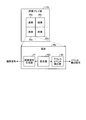
- FIG. 1 is a diagram schematically illustrating a configuration of an example of an imaging device as an electronic apparatus to which the solid-state imaging device according to each embodiment is applied.
- the imaging device 1 includes an optical system 10, a solid-state imaging device 11, a storage unit 12, and a control unit 13.
- the optical system 10 includes one or more lenses and respective mechanisms such as an autofocus mechanism and an aperture mechanism, and guides light from a subject to a light receiving surface of the solid-state imaging device 11.
- the solid-state imaging device 11 includes a pixel including a plurality of light receiving elements for converting incident light into electric signals by photoelectric conversion and outputting the electric signals, and a driving circuit for driving the pixels.
- the solid-state imaging device 11 further includes a signal processing unit that performs predetermined signal processing on a signal output from the pixel and outputs the signal as output data.
- the storage unit 12 stores output data output from the solid-state imaging device 11 in a storage medium.
- a nonvolatile storage medium such as a flash memory or a hard disk drive can be applied.
- the present invention is not limited to this, and a volatile storage medium such as a DRAM (Dynamic Random Access Memory) can be applied to the storage medium.
- DRAM Dynamic Random Access Memory
- the control unit 13 controls the solid-state imaging device 11 to cause the solid-state imaging device 11 to execute an imaging operation for outputting the above-described output data.
- FIG. 2 is a block diagram illustrating a configuration of an example of the solid-state imaging device 11a corresponding to the above-described solid-state imaging device 11 and applicable to the first embodiment.
- the solid-state imaging device 11a includes a pixel array unit 110a, a column arbiter 111, a low arbiter 112, a drive circuit 113a, a signal processing unit 114a, and a control unit 115.
- the pixel array section 110a has a plurality of pixels arranged in a two-dimensional lattice.
- the horizontal arrangement in FIG. 2 is referred to as “row (row)”, and the vertical arrangement with respect to the row is referred to as “column (column)”.
- Each pixel included in the pixel array unit 110a detects an address event based on a plurality of light receiving elements that output a photocurrent corresponding to the received light and a change amount of the photocurrent output from the plurality of light receiving elements.
- An address event detection unit Each pixel outputs a request to the column arbiter 111 and the low arbiter 112 in response to the occurrence of the address event.
- the column arbiter 111 and the low arbiter 112 perform arbitration in cooperation with each other in response to a request output from each pixel included in the pixel array unit 110a, and select an event detection signal output from a specific pixel.
- the selected event detection signal is output from the column arbiter 111.
- the column arbiter 111 and the low arbiter 112 output address information for specifying the pixel that has output the selected event detection signal, together with the event detection signal.
- the drive circuit 113a drives each of the pixels and causes each pixel to execute the address event detection.
- the driving circuit 113a drives each pixel included in the pixel array unit 110a on a row-by-row basis.
- each pixel included in the pixel array unit 110a is driven in a row direction. And an address event detection operation can be executed for each pixel.
- the event detection signal and the address information output from the column arbiter 111 are supplied to the signal processing unit 114a.
- the signal processing unit 114a performs signal processing such as image recognition processing based on the event detection signal and the address information.
- the signal processing unit 114 a outputs event detection data indicating a processing result as output data, and supplies the output data to the storage unit 120.
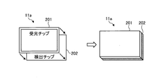
- the solid-state imaging device 11a described with reference to FIG. 2 can be formed, for example, as a stacked CIS (Contact Image Sensor) formed by stacking a plurality of semiconductor chips.
- the solid-state imaging device 11a can be formed with a two-layer structure in which semiconductor chips are stacked in two layers.
- FIG. 3 is a diagram showing an example in which the solid-state imaging device 11a according to the first embodiment is formed by a two-layer stacked CIS.
- a light receiving chip 201 including, for example, a light receiving element is formed on a first layer semiconductor chip, and an address event is detected on a second layer semiconductor chip based on a photocurrent output from the light receiving element.
- a detection chip 202 including an address event detection unit is formed.
- the solid-state imaging device 11a as one device is formed by bonding the first-layer semiconductor chip and the second-layer semiconductor chip while making electrical contact with each other. .
- FIG. 4 is a block diagram illustrating an example of a configuration of the pixel array unit 110a applicable to the first embodiment.
- the pixel array section 110a includes a plurality of pixels 20a arranged in a two-dimensional lattice. 4, each pixel 20a includes an address event detecting unit 30 and a light receiving unit 40a.
- the light receiving section 40a includes a plurality of light receiving elements. Each of the plurality of light receiving elements photoelectrically converts incident light to generate a photocurrent. The light receiving section 40a supplies a photocurrent generated by a light receiving element selected from the plurality of light receiving elements to the address event detecting section 30 under the control of the drive circuit 113a.
- the address event detection unit 30 determines whether or not the amount of change in the photocurrent supplied from the light receiving unit 40a exceeds a threshold, and detects the presence or absence of an address event based on the determination result.
- the address event includes, for example, an up event indicating that the amount of change in the photocurrent has exceeded the ON threshold, and a down event indicating that the amount of change has fallen below the OFF threshold.
- the event detection signal indicating the detection of the address event includes, for example, one bit indicating the detection result of the up event and one bit indicating the detection result of the down event. Note that the address event detection unit 30 can detect only an up event.
- the address event detection unit 30 Upon detecting the occurrence of the address event, the address event detection unit 30 requests the column arbiter 111 and the low arbiter 112 to transmit an event detection signal indicating the occurrence of the address event. When receiving a response to this request from the column arbiter 111 and the low arbiter 112, the address event detection unit 30 supplies an address detection signal to the signal processing unit 114a via the column arbiter 111.
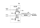
- FIG. 5 is a diagram illustrating a configuration of an example of the light receiving unit 40a according to the first embodiment.
- the light receiving section 40a includes two light receiving elements 401a and 401b each formed of, for example, a photodiode (PD).
- PD photodiode
- the light receiving element 401a has a cathode connected to the ground and an anode connected to the source of the transistor 400a formed by an N-type MOS transistor.
- the drain of the transistor 400a is connected to the address event detector 30.
- the gate of the transistor 400a the signal OFG 1 is supplied.
- Transistor 400a is signal OFG 1 is turned on at a high (High) state, the signal OFG 1 is turned off at a low (Low) state.
- Transistor 400a is in the ON state, the photocurrent Iph 1 output from the light receiving element 401a is supplied to the address event detection unit 30.
- the light receiving element 401b has a cathode connected to the ground and an anode connected to the source of the transistor 400b formed by an N-type MOS transistor.
- the drain of the transistor 400b is connected to the address event detector 30 in common with the drain of the transistor 400a described above.
- the gate of the transistor 400b the signal OFG 2 is supplied.
- Transistor 400b is the signal OFG 2 is turned on in a high state, the off at a low state.
- Transistor 400b is in ON state, the photocurrent Iph 2 output from the light receiving element 401b is supplied to the address event detection unit 30.
- the light receiving element 401a has lower sensitivity than the light receiving element 401b. That is, when the light receiving element 401a and the light receiving element 401b and the same amount of light is incident, a current value of the photocurrent Iph 1 output from the light receiving element 401a is of the photocurrent Iph 2 output from the light receiving element 401b It is smaller than the current value (Iph 1 ⁇ Iph 2 ).
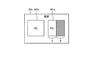
- FIGS. 6A and 6B are diagrams illustrating an example of the pixel 20a including the light receiving elements 401a and 401b having different sensitivities. Note that, in FIGS. 6A and 6B, the light receiving elements 401a and 401b are described as PD 1 and PD 2, respectively.
- FIG. 6A is an example in which the areas of the light receiving portions in the light receiving elements 401a and 401b are made different to form a sensitivity difference.
- the area of the light receiving section of the light receiving element 401a is smaller than the area of the light receiving section of the light receiving element 401b.
- the light receiving element 401a performs less photoelectric conversion than the light receiving element 401a. Therefore, the light sensitivity of the light receiving element 401a is lower than that of the light receiving element 401b.
- FIG. 6B shows an example in which the light receiving elements 401a and 401b have the same configuration and the light receiving section has the same area, while a part (half in the example of FIG. 6B) of the light receiving section of the light receiving element 401a is shielded by a mask or the like. It is.
- the light applied to the light receiving element 401a is incident on the light receiving section in the opening area A, and is not incident on the light receiving section in the light shielding area B. Therefore, the areas of the light receiving portions of the light receiving elements 401a and 401b are substantially different, and the light sensitivity of the light receiving element 401a is lower than that of the light receiving element 401b, as in the example of FIG. 6A.
- FIG. 7 is a diagram schematically illustrating an example of wiring in the pixel array unit 110a according to the first embodiment.
- Drive circuit 113a generates a signal OFG 1 and OFG 2 under the control of the control unit 115, the generated these signals OFG 1 and OFG 2, supplied to each pixel 20a.
- the drive circuit 113a for each pixel 20a arranged in a two-dimensional lattice shape on the pixel array section 110a, and generates a signal OFG 1 and OFG 2 for each row.
- each pixel 20a is connected to the lower arbiter 112 on a row-by-row basis for transmitting and receiving requests and responses.
- each pixel 20a is connected to the column arbiter 111 on a column basis for transmitting and receiving a request and a response, and supplying an event detection signal indicating the detection of an event and address information.
- the column arbiter 111 supplies the event detection signal and the address information supplied from the pixel 20a to the control unit 115.
- the control unit 115 specifies a row to be switched between the high / low state of the signals OFG 1 and OFG 2 based on the event detection signal and the address information supplied from the column arbiter 111.
- Controller 115 an instruction of switching the high / low state of the signal OFG 1 and OFG 2 in a particular row, and supplies to the drive circuit 113a.
- Drive circuit 113a switches between the high / low state of signals OFG 1 and OFG 2 in the row in response to this instruction.
- the signal OFG 1 and OFG 2 is have been supplied in units of rows of pixels 20a included in the pixel array section 110a, which is not limited to this example.
- a signal OFG 1 and OFG 2 may be supplied collectively to all the pixels 20a included in the pixel array section 110a, the pixel array section 110a, a plurality of blocks including a predetermined number of pixels 20a
- the signal may be divided and the signals OFG 1 and OFG 2 may be supplied in block units.
- FIG. 8 is a diagram showing the configuration of the address event detection unit 30 applicable to the first embodiment in more detail.
- the address event detection unit 30 includes a current-voltage conversion unit 300, a buffer amplifier 310, a subtraction unit 320, and a quantizer 330.
- the current-voltage converter 300 includes transistors 301 and 303 using N-type MOS transistors and a transistor 302 using P-type MOS transistors.
- the description is given on the assumption that the light receiving element 401a is a photodiode.
- FIG. 8 shows only the light receiving element 401a among the light receiving elements 401a and 401b included in the light receiving section 40a, and omits the description of the transistor 400a for the sake of explanation.
- the source of the N-type transistor 301 is connected to the light receiving element 401a, and the drain is connected to the power supply terminal.
- the P-type transistor 302 and the N-type transistor 303 are connected in series between a power supply terminal and a ground terminal.
- a connection point between the drain of the transistor 302 and the drain of the transistor 303 is connected to the gate of the transistor 301 and the input terminal of the buffer amplifier 310.
- a predetermined bias voltage Vbs is applied to the gate of the transistor 302.
- the drains of the N-type transistors 301 and 303 are connected to the power supply side, and form source followers.
- the photocurrent output from the light receiving element 401a is converted into a logarithmic voltage signal by the two source followers connected in a loop. Further, the transistor 302 supplies a constant current to the transistor 303.
- Subtraction unit 320 includes capacitors 321 and 322 having capacitances C 1 and C 2 , a switch unit 323, and an inverter 324, respectively.
- Capacitor 322 is connected in parallel to inverter 324.
- the switch unit 323 switches a path connecting both ends of the capacitor 322 between an on state and an off state according to a row drive signal.
- Inverter 324 inverts the voltage signal input via capacitor 321.
- the inverter 324 supplies the inverted signal to the quantizer 330.
- the electric charge Q 2 stored in the capacitor 322 is expressed by the following equation (3), where the output voltage of the inverter 324 is V out .
- Q 2 ⁇ C 2 ⁇ V out (3)
- Equation (5) represents a subtraction operation of the voltage signal, and the gain of the subtraction result is a ratio C 1 / C 2 of the capacitance of the capacitors 321 and 322.
- the capacity C 1 of the capacitor 321 also preferably designed to have a small capacitance C 2 of the capacitor 322.
- the capacitance C 2 of the capacitor 322 is too small, there is a possibility that kTC noise increases, the noise characteristic deteriorates. Therefore, reduction of the capacitance C 2 of the capacitor 322 is limited to a range that can tolerate the noise.
- the address event detection unit 30 including a subtraction unit 320 is mounted on each of the pixels 20, the capacitance C 1 and C 2 of the capacitors 321 and 322, there is a restriction on the area. In consideration of these, the values of the capacitances C 1 and C 2 of the capacitors 321 and 322 are determined.
- the quantizer 330 detects three states of an up event, a down event, and no event detection using two thresholds of an ON threshold and an OFF threshold. Therefore, the quantizer 330 is called a 1.5-bit quantizer.
- FIG. 9 is a diagram for explaining the operation of the address event detection unit 30 shown in FIG.
- the horizontal axis represents time
- the vertical axis represents voltage.
- 9 shows an example of the output voltage Vp of the current-voltage converter 300.
- the lower part of FIG. 9 illustrates the state of the voltage V diff , which is the output voltage of the subtractor 320, corresponding to the change of the upper output voltage Vp.
- the voltage V diff corresponds to the voltage V out in the above equation (5).
- the OFF threshold and the ON threshold are thresholds for the voltage V diff for detecting a down event and an up event, respectively.
- the voltage V diff exceeds the OFF threshold in the positive direction, an up event is detected.
- the voltage V diff exceeds the ON threshold in the negative direction, a down event is detected. If the voltage V diff is less than the OFF threshold and greater than the ON threshold, it is determined that no event is detected.
- the output voltage Vp output from the current-to-voltage converter 300 is input to the subtractor 320 via the buffer amplifier. First, a case where the amount of light received by the light receiving element 401a increases and the output voltage Vp output from the current-voltage converter 300 increases will be described.
- the output voltage Vp from the time t 0 increases, at time t 1, it is assumed that the voltage V diff is a difference from the output voltage Vp at the time t 0 of the output voltage Vp exceeds the ON threshold in the negative direction.
- the quantizer 330 outputs an event detection signal indicating up event detection.
- the row drive circuit 110 switches the switch section 323 to the ON state, and the output of the subtraction section 320 is set to the reset level.
- the row drive circuit 110 switches the switch unit 323 to the off state immediately after setting the output of the subtraction unit 320 to the reset level.
- the row drive circuit 110 switches the switch section 323 to the ON state, and the output of the subtraction section 320 is set to the reset level.
- the row drive circuit 110 switches the switch unit 323 to the off state immediately after setting the output of the subtraction unit 320 to the reset level.
- the address event detection unit 30 compares the difference between the output voltage Vp of the current-voltage conversion unit 300 with the ON threshold value and the OFF threshold value, as described above, to obtain an event detection signal corresponding to a change in the amount of light received by the light receiving element 401a. Can be output.
- the voltage Vp ′ is obtained by rewriting the change of the output voltage Vp of the current-voltage converter 300 in the lower part of FIG. 9, that is, according to the output of the quantizer 330. From the determination result based on the change in the voltage Vp ′ and the ON threshold value and the OFF threshold value based on the voltage Vdiff , the quantizer 330 determines, in other words, the rise and fall of the change in the voltage Vp ′ for each ON threshold value and OFF threshold value. Is detected.
- FIG. 10 is a diagram illustrating an example of the Vg-Id characteristic of the transistor 301, which is an N-type MOS transistor, used in the current-voltage converter 300 (see FIG. 8) according to the first embodiment.
- the horizontal axis represents the gate voltage Vg
- the vertical axis represents the drain current Id (ln) in logarithmic representation.
- the Vg-Id characteristic of the transistor 301 shifts from the OFF region to the sub-threshold region and further shifts from the sub-threshold region to the saturation region as the gate voltage Vg increases.
- the OFF region is a region where the drain current Id is substantially constant with an increase in the gate voltage Vg.
- the sub-threshold region is a region where the drain current Id increases logarithmically as the gate voltage Vg increases.
- the saturation region is a region where the drain current Id increases substantially linearly as the gate voltage Vg increases.
- the current-to-voltage converter 300 converts the photocurrent Iph output from the light receiving element 401a into a voltage by logarithmic conversion to obtain an output voltage Vp using the characteristics of the sub-threshold region. Therefore, a range 420 corresponding to the range of the gate voltage Vg in the sub-threshold region is a detection range of the photocurrent Iph output from the light receiving element 401a. As described above, the light detection range (dynamic range) of the address event detection unit 30 is limited to the current range of the sub-threshold region of the transistor that performs the current-voltage conversion.
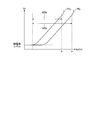
- FIG. 11 is a diagram illustrating an example of input / output characteristics of the current-voltage converter 300 applicable to the first embodiment.
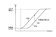
- the horizontal axis represents the photocurrent Iph output from the light receiving element 401a or 401b as a logarithm, and the vertical axis represents the output voltage Vp of the current-voltage converter 300. Note that FIG. 11 corresponds to a diagram in which the vertical axis and the horizontal axis of the graph of FIG. 10 are interchanged.
- characteristic lines PD 1 and PD 2 shows a characteristic example of light receiving elements 401a of the low sensitivity described with reference to FIG. 5, a characteristic example of the light receiving element 401b of the normal speed, respectively.
- the dark current level is a voltage level obtained by converting a dark current generated in the light receiving elements 401a and 401b into a voltage.
- the dark current level is the lower limit value of the output voltage Vp of the current-voltage converter 300.
- the light receiving element 401a of the low sensitivity the current value of the photocurrent Iph 1 is output when the light receiving element 401b in the same amount of normal sensitivity is incident, output from the light receiving element 401b the current value of the current Iph 2 smaller.
- the light-receiving element 401a of the low sensitivity even if light enters a large amount, the photocurrent Iph 1 is small is output. Therefore, the characteristic line PD 1 of the light receiving element 401a, to the characteristic line PD 2 of the light-receiving element 401b, shifts (to the right in FIG. 11) direction of larger photocurrent Iph.
- a current value a of the photocurrent Iph 1 by the light receiving element 401a is, the photocurrent Iph according to the light receiving element 401b It shifted to the larger side with respect to second current value b.
- light detection for detecting an address event is performed using both a low-sensitivity light receiving element 401a and a normal-sensitivity light receiving element 401b.
- FIGS. 12A and 12B are diagrams for explaining control for performing address event detection using the low-sensitivity light-receiving element 401a and the normal-sensitivity light-receiving element 401b according to the first embodiment.
- FIG. 12A shows an example in which an address event detection by the address event detection unit 30 based on the photocurrent Iph 1 output from the light receiving element 401a.
- a signal OFG 1 supplied to the gate of the transistor 400a and the high state the signal OFG 2 supplied to the gate of the transistor 400b and the low state.
- the transistor 400a is turned on, the transistor 400b is turned off, and the photocurrent Iph 1 output from the light receiving element 401a, the photoelectric current Iph 2 output from the light receiving element 401b, of the photocurrent Iph 1 is transistor
- the signal is supplied to the address event detection unit 30 via the signal 400a.
- FIG. 12B shows an example in which an address event detection by the address event detection unit 30 based on the photocurrent Iph 2 output from the light receiving element 401b.
- a signal OFG 1 supplied to the gate of the transistor 400a and a low state the signal OFG 2 supplied to the gate of the transistor 400b and the high state.
- the transistor 400a is turned off, the transistor 400b is turned on, the photocurrent Iph 1 output from the light receiving element 401a, the photoelectric current Iph 2 output from the light receiving element 401b, of the photocurrent Iph 2 the transistor
- the data is supplied to the address event detection unit 30 via the line 400b.
- Address event detection unit 30 thus, of the photocurrent Iph 1 and Iph 2, and outputs an event detection signal based on a signal OFG 1 and OFG photocurrent Iph det selected according to 2.
- FIG. 13 is a diagram illustrating an example of a configuration of the current-voltage converter 300a to which the limiter is applied according to the first embodiment.
- FIG. 13 omits the buffer amplifier 310, the subtraction unit 320, and the quantizer 330 in the address event detection unit 30 shown in FIG.
- the current-voltage converter 300a has a configuration in which a transistor 304, which is a P-type MOS transistor, is added as a limiter to the current-voltage converter 300 of FIG. More specifically, the source of the transistor 304 is connected to the output path of the event detection signal of the current-voltage converter 300a, that is, the connection point between each drain of the transistors 302 and 303 and the gate of the transistor 301, The drain of 304 is connected to ground.
- a transistor 304 which is a P-type MOS transistor
- the upper limit of the voltage value of the event detection signal output from the current-voltage converter 300a can be limited to a voltage corresponding to the limit voltage Lt.
- the description will be given on the assumption that the upper limit of the voltage value of the event detection signal output from the current-voltage converter 300a is limited to the limit voltage Lt.
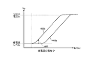
- FIG. 14 is a diagram illustrating an example of input / output characteristics of the current-voltage converter 300a according to the first embodiment.
- the horizontal axis represents the logarithm of the photocurrent Iph output from the light receiving element 401a or 401b
- the vertical axis represents the output voltage Vp of the current-voltage converter 300.
- the input / output characteristics of the current / voltage converter 300a are such that the output voltage Vp in the input / output characteristics of the current / voltage converter 300 in FIG. 11 is limited by the limit voltage Lt.
- the output voltage Vp usually based on the photocurrent Iph 2 of the light-receiving element 401b of sensitivity, corresponding to the voltage of the saturation point, the current value b of the photocurrent Iph 2 by the light receiving element 401b, is limited to the limit voltage Lt You.
- the photocurrent Iph det used for address event detection using the mechanism of address event detection process, the photocurrent Iph 1 output from the light receiving element 401a of the low sensitivity, It switched between photocurrent Iph 2 outputted from the light receiving element 401b of the normal speed.
- the switching process according to the first embodiment will be described with reference to FIGS.
- the signal OFG 1 is a high state, it is assumed that the photocurrent Iph 1 output from the light receiving element 401a of the low sensitivity are supplied to the address event detection section 30a.
- Figure 15 is a diagram showing an example of a variation of the photocurrent Iph 1 output from the light receiving element 401a of the low sensitivity.
- both ends of a change of the photocurrent Iph 1 is defined by a dark current level and limit voltage Lt.
- Figure 16 corresponds to a change of the photocurrent Iph 1 in FIG. 15 is a timing chart showing an example of processing in the solid-state imaging device 11a.
- a chart (a 1 ) shows an example of a change in the photocurrent Iph 1 output from the low-sensitivity light receiving element 401a (low-sensitivity PD).
- it is output photocurrent Iph 2 even in the light-receiving element 401b of the normal speed (normal sensitivity PD), showing an example of a variation of the photocurrent Iph 2, in the chart of FIG. 16 (b 1) .
- a chart (e 1 ) shows an example of an event detection signal output from the address event detection unit 30a.
- event detection signal corresponding to the change of the photocurrent Iph 1 of low sensitivity PD shown in chart (a 1), are output at time t 10, t 11 and t 12.
- Charts (c 1 ) and (d 1 ) show examples of arbitration for the event detection signal output from the pixel 20a including the low-sensitivity PD and the normal sensitivity PD in the low arbiter 112 and the column arbiter 111, respectively.
- the event detection signal shown in the chart (e 1 ) is selected.
- charts (f 1 ) and (g 1 ) show the states of the signals OFG 1 and OFG 2 , respectively. Initially, the signal OFG 1 is set to the high state and the signal OFG 2 is set to the low state, and the photocurrent Iph 1 output from the low-sensitivity PD shown in the chart (a 1 ) is supplied to the address event detection unit 30.
- the control unit 115 acquires the event detection signal from the column arbiter 111, based on the acquired event detection signal, predicts that the photocurrent Iph 1 in the low-sensitivity PD, and a variation of the photocurrent Iph 1.
- Control unit 115 when the amount of change predicted photocurrent Iph 1 exceeds a predetermined amount, switches low signal OFG 1 state, the signal OFG 2 in the high state (time t 13). Accordingly, the photocurrent Iph 2 normal sensitivity PD is supplied to the address event detection unit 30.
- the address event detection unit 30 detects a down event when the amount of change exceeds the OFF threshold in the positive direction, and detects an up event when the amount of change exceeds the ON threshold in the negative direction (see FIG. 9).
- the address event detection unit 30 detects an up event assuming that the amount of change has exceeded the OFF threshold in the positive direction, and outputs an event detection signal (time t 14 ).
- Column arbiter 111 and Roabita 112 selects an event detection signal at this time t 14.
- Control unit 115 acquires the event detection signal from the column arbiter 111 returns a signal OFG 1 to a high state (time t 15), returning the signal OFG 2 to a low state (time t 16). Thereafter, the address event detection unit 30 performs the address event detection by continuously using the low-sensitivity PD selected in the initial state (for example, at time t 17 ).
- FIGS. Figure 17 corresponds to Figure 15 described above, is a diagram illustrating an example of a change of the photocurrent Iph 1 output from the light receiving element 401a of the low sensitivity.
- the lower end of the change of the photocurrent Iph 1 it is hanging on the dark current level.
- the amount of change in light intensity that causes a change of the photocurrent Iph 1 may amount variation greater possibility shown in the variation photocurrent Iph 1.
- Figure 18 corresponds to a change of the photocurrent Iph 1 in FIG. 17 is a timing chart showing an example of processing in the solid-state imaging device 11a. Note that the meanings of the respective charts (a 2 ) to (g 2 ) in FIG. 18 are the same as those of the respective charts (a 1 ) to (g 1 ) of FIG. 16 described above, and thus description thereof will be omitted. Also in the example of FIG. 18, similarly to FIG. 16 described above, as shown in the chart (e 2 ), the event detection signal corresponding to the change in the photocurrent Iph 1 of the low-sensitivity PD is changed at time t 20 , It is output at t 21 and t 22.
- the signal OFG 1 is initially in the high state
- the signal OFG 2 is in the low state
- the low sensitivity PD shown in the chart (a 2 ) photocurrent Iph 1 to be output is supplied to the address event detection unit 30.
- control unit 115 similarly to the explanation in FIG. 16, based on the event detection signal acquired from the column arbiter 111, predicts the photocurrent Iph 1 in the low-sensitivity PD, and a variation of the photocurrent Iph 1.
- Control unit 115 when the amount of change predicted photocurrent Iph 1 exceeds a predetermined amount, switches low signal OFG 1 state, the signal OFG 2 in the high state (time t 23). Accordingly, the photocurrent Iph 2 normal sensitivity PD is supplied to the address event detection unit 30.
- the address event detection unit 30 determines that the amount of change does not exceed the ON threshold value and the OFF threshold value, and determines that no event is detected, and as illustrated in a range surrounded by a dotted line in FIG. Does not output event detection signal. Thereby, the low-sensitivity PD is excluded from the target of the address event detection, and the normal sensitivity PD is the target of the address event detection.
- the address event detection unit 30, performs address event detection based on the photocurrent Iph 2 normal sensitivity PD shown in chart (b 2) of FIG. 18, the amount of change in time t 24 is the OFF threshold A down event is detected as having exceeded the forward direction, and an event detection signal is output.
- Column arbiter 111 and Roabita 112 selects an event detection signal at this time t 24.
- the control unit 115 maintains the low state of the signal OFG 1 and the high state of the signal OFG 2 even if the event detection signal is obtained from the column arbiter 111, and the normal sensitivity switched from the low sensitivity PD at time t 23 .
- the address event is detected using the PD.
- the optical current Iph det used for address event detection, the photocurrent Iph 1 output from the low-sensitivity PD (light receiving element 401a), usually sensitivity PD (light receiving element 401b) outputs the control of switching between the photocurrent Iph 2, can be performed by utilizing the structure for the address event detection.
- the signal OFG 1 and OFG 2 are supplied in units of rows of pixels 20a included in the pixel array portion 110a. Therefore, in each pixel 20a, unable to hold the selection state by the signal OFG 1 and OFG 2.
- the selection state by the signals OFG 1 and OFG 2 for each pixel 20 a can be held.
- FIG. 19 is a diagram schematically illustrating an example of wiring in a pixel array unit 110b according to a modification of the first embodiment.
- the above-described pixels 20a are arranged in a two-dimensional lattice, and the terminals Tm 1 and Tm 2 of the switch 21 are connected to each pixel 20a.
- terminal Tm 1 of switch 21 is connected to the gate of transistor 400a in light receiving unit 40a included in pixel 20a
- terminal Tm 2 is connected to the gate of transistor 400b in light receiving unit 40a.
- the drive circuit 113b generates a signal OFG for each row under the control of the control unit 115, and supplies the generated signal OFG to each pixel 20a via a common terminal Tc of the switch 21 connected to each pixel 20a.
- the switch 21 selects one of the terminals Tm 1 and Tm 2 according to the selection signal SL supplied from the drive circuit 113b.
- the drive circuit 113b generates each selection signal SL corresponding to each pixel 20a under the control of the control unit 115, and supplies the selection signal SL to the switch 21 connected to each pixel 20a for each row. Note that FIG. 19 shows that a plurality of selection signals SL are supplied as the selection signal SLs.
- the selection state of the terminals Tm 1 and Tm 2 in each switch 21 according to a certain selection signal SL is held until the next selection signal SL is supplied.
- a photoelectric current Iph 1 by the light receiving element 401a of the low sensitivity, the optical current Iph 2 by the light receiving element 401b of the normal speed, the selected state can be maintained.
- the switch 21 is shown to be provided outside the pixel 20a, but this is not limited to this example, and the switch 21 may be provided inside the pixel 20a.
- the selection signal SL is supplied to each of the pixels 20a.
- the present invention is not limited to this example.
- a logic circuit for switching the terminals Tm 1 and Tm 2 of the switch 21 according to a specific bit string may be provided for each pixel 20a. By doing so, it is possible to reduce the number of signal lines for supplying the selection signal SLs.
- one switch 21 is connected to one pixel 20a, but this is not limited to this example, and one switch 21 can be shared by a plurality of pixels 20a.
- FIG. 20 is a diagram illustrating a configuration of an example of a pixel 20b according to the second embodiment.
- the pixel 20b includes a light receiving unit 40b and a current-voltage conversion unit 300.
- the current-voltage converter 300 has the same configuration as the current-voltage converter 300 described with reference to FIG. Note that the limiter (transistor 304) described with reference to FIG. 13 may be added to the current-voltage converter 300 in FIG.
- the light receiving unit 40b includes light receiving elements 401c and 401d having substantially the same sensitivity.
- the light receiving element 401c has a cathode connected to the ground and an anode connected to the source of the transistor 400a formed by an N-type MOS transistor.
- the drain of the transistor 400a is connected to a connection point where the source of the transistor 301 of the current-voltage converter 300 and the gate of the transistor 303 are connected.
- the gate of the transistor 400a, the signal OFG 1 is supplied.
- the light receiving element 401d has a cathode connected to the ground and an anode connected to the source of the transistor 400b formed by an N-type MOS transistor.
- the drain of the transistor 400b is connected to a connection point where the source of the transistor 301 of the current-voltage converter 300 and the gate of the transistor 303 are connected in common with the drain of the transistor 400a.
- the gate of the transistor 400b, the signal OFG 2 is supplied.
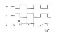
- FIG. 21 is a time chart illustrating an example of a driving method of the light receiving unit 40b according to the second embodiment.
- charts (h) and (i) show the states of the signals OFG1 and OFG2, respectively, and chart (j) shows the output voltage Vp output from the current-voltage converter 300.
- the control unit 115 acquires the output voltage Vp output from the current-voltage conversion unit 300 in synchronization with the switching timing, and sets the output voltage Vp 1 when the signal OFG 1 is in a high state and the signal OFG 2 to be high.
- the output voltage Vp 2 in the state is compared with the output voltage Vp 2 to obtain a difference 406 between the output voltages Vp 1 and Vp 2 .
- This photocurrent Iph 1 output from the light receiving element 401c corresponds to the process of obtaining a photoelectric current Iph 2 output from the light receiving element 401d, the difference.
- the control unit 115 treats the difference 406 as an event detection signal and analyzes the difference 406 in the control unit 115 or outside.
- FIGS. 22A, 22B, and 22C are diagrams illustrating an example of a configuration of light receiving elements 401c and 401d applicable to the second embodiment.
- FIG. 22A shows an example of a pixel 20b (a) in which light receiving elements 401c and 401d are arranged in parallel.
- information on the edge of the image can be obtained based on the difference 406.
- FIG. 22B shows an example of a pixel 20b (b) in which the light receiving elements 401c and 401d are arranged in parallel and adjacent to each other, and a portion adjacent to the light receiving elements 401c and 401d is shielded by using a light shielding pattern 407.
- the light shielding pattern 407 is, for example, a metal light shielding pattern.
- the light incident on the pixel 20b (b) is received by the light receiving elements 401c and 401d from the openings not shielded by the light shielding pattern 407.
- FIG. 23 is a diagram schematically showing how light is incident on the light receiving elements 401c and 401d in the pixel 20b (b) of FIG. 22B.
- a light-shielding pattern 407 is provided on the light receiving elements 401c and 401d arranged adjacent to each other, and a lens 440 is provided corresponding to the pixel 20b (b).
- the lens 440 is, for example, an OCL (On Chip Lense).
- the light incident on the lens 440 is applied to the pixel 20b (b), and this light is shielded by the light-shielding pattern 407, and is located on the right side of the light receiving element 401c and the left side of the light receiving element 401d in FIG. Is not incident.
- Light 409a on the left side of the lens 440 in FIG. 23 is incident on the left side of the light receiving element 401c which is not shielded.
- Light 409b on the right side is incident on the unshielded right side of the light receiving element 401d.
- the pixel 20b (b) can be used as an image plane phase difference pixel.
- the image plane phase difference pixel is usually formed by stacking an aperture filter having an opening on the left half of the light receiving surface of the light receiving element, for example, and opening the pixel on the right half of the light receiving surface of the other light receiving element. And a pixel on which the aperture filter is stacked, as a set, and distance measurement is performed based on a phase difference of light received by the two pixels.
- FIG. 22B it is possible to form an image plane phase difference pixel with one pixel 20b (b).
- FIG. 22C shows an example of a pixel 20b (c) in which a polarization filter 408 is provided for the light receiving elements 401c and 401d with different polarization directions.
- the polarizing filter 408 can be formed by a metal light-shielding pattern in which a number of slits through which light passes are provided in parallel. As described above, by making the polarization directions of the light receiving elements 401c and 401d included in the pixel 20b (c) different, the polarization can be detected by one pixel 20b (c).
- the control unit 115 the signal OFG 1 is the time of transition from a high state to a low state, to obtain the output voltage Vp 1 of the photocurrent Iph output from the light receiving element 401c is converted.
- the signal OFG 2 is shifted to a high state.
- Control unit 115, the signal OFG 2 is the time of transition from the high state to a low state, to obtain the output voltage Vp 2 photocurrent Iph output from the light receiving element 401d is converted.
- the control unit 115 calculates a difference 406 between the output voltages Vp 1 and Vp 2 , and it is assumed that an address event is detected when the difference 406 exceeds an ON threshold or an OFF threshold in a predetermined direction.
- the pixel 20b including the light receiving elements 401c and 401d having the same sensitivity can be used for various uses.
- the address event detection is performed based on the change in the photocurrent Iph output from the light receiving element.
- an address event is detected by further using a pixel signal corresponding to the absolute value of the photocurrent Iph output from the light receiving element.
- FIG. 24 is a block diagram illustrating a configuration of an example of the solid-state imaging device according to the third embodiment, which corresponds to the solid-state imaging device 11 described with reference to FIG. 24,
- the solid-state imaging device 11c includes a pixel array unit 110c, a column arbiter 111, a low arbiter 112, a row driving circuit 113c, a signal processing unit 114c, a control unit 115, and a column driving circuit 116.
- the row driving circuit 113c includes the function of the driving circuit 113a shown in FIG.
- the pixel array section 110c has a plurality of pixels arranged in a two-dimensional lattice like the pixel array section 110a described with reference to FIG.
- Each of the pixels has a plurality of light receiving elements for outputting a photocurrent Iph corresponding to the received light, and an address event for detecting an address event based on a change amount of the light current Iph output from the plurality of light receiving elements.
- a detection unit; and a pixel signal generation unit that generates a pixel signal which is an analog signal of a voltage corresponding to the absolute value of the photocurrent Iph.
- the row driving circuit 113c has a function of driving each of the pixels and outputting a pixel signal to the column driving circuit 116, in addition to the function of the driving circuit 113a of FIG.
- the column driving circuit 116 includes an AD (Analog to digital) converter for each column, and a driving circuit for scanning the AD converter for each column in the row direction.
- the AD converter for each column is called a column ADC (AD converter).
- the column drive circuit 116 scans the column ADC in the row direction, and outputs a pixel signal converted into a digital signal by each AD converter in row units.
- the pixel signal output from the column driving circuit 116 is supplied to the signal processing unit 114c.
- the signal processing unit 114c performs predetermined signal processing such as CDS (Correlated Double Sampling) processing and AGC (Auto Gain Control) processing on the digital pixel signal supplied from the column driving circuit 116. Further, signal processing such as image recognition processing is performed on the event detection signal supplied from the column arbiter 111. The signal processing unit 114c supplies the data indicating the processing result and the event detection signal to the storage unit 120.
- predetermined signal processing such as CDS (Correlated Double Sampling) processing and AGC (Auto Gain Control) processing
- CDS Correlated Double Sampling
- AGC Automatic Gain Control
- FIG. 25 is a block diagram illustrating a configuration of an example of a pixel array unit 110c according to the third embodiment.
- the pixel array unit 110c includes a plurality of pixels 20c arranged in a two-dimensional lattice.
- each pixel 20c includes an address event detecting unit 30, a light receiving unit 40c, and a pixel signal generating unit 41.
- the light receiving section 40c includes a plurality of light receiving elements, and photoelectrically converts incident light to generate a photocurrent Iph.
- the light receiving unit 40c supplies the generated photocurrent Iph to one of the pixel signal generation unit 41 and the address event detection unit 30 under the control of the row driving circuit 113c.
- the address event detection unit 30 Upon detecting the occurrence of the address event, the address event detection unit 30 requests the column arbiter 111 and the low arbiter 112 to transmit an event detection signal indicating the occurrence of the address event. When receiving a response to this request from the column arbiter 111 and the low arbiter 112, the address event detection unit 30 supplies an address detection signal to the row drive circuit 113c and the signal processing unit 114c.
- the address event detection unit 30 includes the current-voltage conversion unit 300a described with reference to FIG. 13 and which limits the upper limit of the output voltage Vp to the limit voltage Lt by the limiter.
- the pixel signal generation unit 41 generates a signal of a voltage corresponding to the photocurrent Iph supplied from the light receiving unit 40c as a pixel signal.
- the pixel signal generation unit 41 supplies the generated pixel signal to the column driving circuit 116 via a vertical signal line.
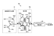
- FIG. 26 is a diagram illustrating a configuration of an example of a pixel 20c according to the third embodiment.
- the light receiving section 40c includes, for example, two light receiving elements 401a and 401b each formed of, for example, a photodiode, and transistors 400a, 400b, 402a, and 402b, which are N-type MOS transistors.
- the pixel signal generation unit 41 includes a floating diffusion layer 413, and a reset transistor 410, an amplification transistor 411, and a selection transistor 412, each of which is an N-type MOS transistor.
- the light receiving element 401a has a cathode connected to the ground, and an anode connected to the source of the transistor 400a formed of an N-type MOS transistor and the drain of the transistor 402a formed of an N-type MOS transistor.
- the drain of the transistor 400a is connected to the address event detector 30.
- the source of the transistor 402a is connected to the floating diffusion layer 413 in the pixel signal generator 41.
- Transistor 400a is signal OFG 1 is turned on in a high state, signal OFG 1 is turned off in a low state.
- the gate of the transistor 400b, the signal OFG 2 is supplied.
- Transistor 400b is the signal OFG 2 is turned on in a high state, signal OFG 2 is turned off in a low state.
- Transistor 400a is in the ON state, the photocurrent Iph 1 output from the light receiving element 401a is supplied to the address event detection unit 30.
- the transistor 400b is in ON state, the photocurrent Iph 2 output from the light receiving element 401b is supplied to the address event detection unit 30.
- Transistor 402a is signal TRG 1 is turned on in a high state, signal OFG 1 is turned off in a low state.
- the gate of the transistor 402b, the signal TRG 2 is supplied.
- Transistor 402b is the signal TRG 2 is turned on in a high state, signal TRG 2 is turned off in a low state.
- Transistor 402a is in the ON state, the photocurrent Iph 1 output from the light receiving element 401a is supplied to the pixel signal generation section 41.
- the transistor 402b is in ON state, the photocurrent Iph 2 output from the light receiving element 401b is supplied to the pixel signal generation section 41.
- the floating diffusion layer 413 accumulates charges and generates a voltage corresponding to the amount of the accumulated charges.
- the reset transistor 410 initializes the charge amount of the floating diffusion layer 413 according to a reset signal RST supplied from the row drive circuit 113c.
- the amplification transistor 411 amplifies the voltage of the floating diffusion layer 413.
- the selection transistor 412 outputs the voltage signal amplified by the amplification transistor 411 as a pixel signal SIG to the column driving circuit 116 via the vertical signal line VSL according to the selection signal SEL from the row driving circuit 113c.
- the sensitivity of the light receiving element 401a is lower than that of the light receiving element 401b.
- the light receiving element 401a is referred to as a low sensitivity PD and the light receiving element 401b is referred to as a normal sensitivity PD as appropriate.
- FIG. 27 is a diagram schematically illustrating an example of wiring in a pixel array unit 110c according to the third embodiment. Similar to the drive circuit 113a of the pixel array unit 110a according to the first embodiment described with reference to FIG. 7, row drive circuit 113c is controlled to generate a signal OFG 1 and OFG 2 in accordance with the control unit 115, to generate These signals OFG 1 and OFG 2 are supplied to each pixel 20c. In the example of FIG. 27, the row drive circuit 113c, for each pixel 20c arranged in a two-dimensional lattice shape on the pixel array unit 110c, and generates a signal OFG 1 and OFG 2 for each row.
- Row drive circuit 113c further generates a signal TRG 1 and TRG 2 under the control of the control unit 115, the generated these signals TRG 1 and TRG 2, supplied to each pixel 20c.
- the row drive circuit 113c for each pixel 20c arranged in a two-dimensional lattice shape on the pixel array unit 110c, and generates a signal TRG 1 and TRG 2 for each row.
- the vertical signal line VSL of each pixel 20c is connected to the column drive circuit 116 for each column of each pixel 20c arranged in the pixel array unit 110c.
- the row drive circuit 113c further arranges the above-described reset signal RST and selection signal SEL in the pixel array unit 110c in a two-dimensional grid pattern under the control of the control unit 115. Is generated for each row for each pixel 20c. The row drive circuit 113c supplies the generated reset signal RST and selection signal SEL to each pixel 20c.
- FIGS. 28A and 28B are diagrams for describing control of the light receiving unit 40c according to the third embodiment.
- Figure 28A shows an example of a case where the address events detected by the address event detection unit 30 based on the photocurrent Iph 1 output from the light receiving element 401a is a low-sensitivity PD.
- a signal OFG 1 supplied to the gate of the transistor 400a and the high state the signal OFG 2 supplied to the gate of the transistor 400b and the low state.
- a signal TRG 1 supplied to the gate of the transistor 402a and a low state the signal TRG 2 supplied to the gate of the transistor 402b and the high state.
- the transistor 400a is turned on, the transistor 400b is turned off, the transistor 402a is turned off, and the transistor 402b is turned on.
- Photocurrent Iph 1 output from the light receiving element 401a is low sensitivity PD
- the photoelectric current Iph 2 output from the light receiving element 401b is generally sensitive PD
- the optical current Iph 2 is supplied to the pixel signal generating section 41 via the transistor 402b.
- Figure 28B shows an example of a case where the address events detected by the address event detection unit 30 based on the photocurrent Iph 2 output from the light receiving element 401b is generally sensitive PD.
- a signal OFG 1 supplied to the gate of the transistor 400a and a low state the signal OFG 2 supplied to the gate of the transistor 400b and the high state.
- a signal TRG 1 supplied to the gate of the transistor 402a and the high state the signal TRG 2 supplied to the gate of the transistor 402b and the low state.
- the transistor 400a is turned off, the transistor 400b is turned on, the transistor 402a is turned on, and the transistor 402b is turned off.
- Photocurrent Iph 1 output from the light receiving element 401a is low sensitivity PD
- the photoelectric current Iph 2 output from the light receiving element 401b is generally sensitive PD
- the optical current Iph 2 is supplied to the pixel signal generating section 41 via the transistor 402a.
- FIG. 29 is a timing chart illustrating an example of processing in the solid-state imaging device 11c according to the third embodiment.
- charts (k) and (n) show examples of the reset signal RST and the selection signal SEL generated in the row drive circuit 113c.
- Chart (o) shows an example of the voltage of the pixel signal on the vertical signal line VSL.
- charts (l) and (m) show examples of signals TRG 1 and TRG 2 generated in row driving circuit 113c
- charts (s) and (t) show signals in row driving circuit 113c.
- An example of generated signals OFG 1 and OFG 2 is shown.
- chart (r) shows an example of an event detection signal output from the address event detection unit 30.
- Charts (p) and (q) show examples of arbitration for the event detection signal shown in chart (r) in the lower arbiter 112 and the column arbiter 111, respectively. In each of the high states, the event detection signal shown in the chart (r) is selected.
- the signal OFG 1 is set to a high state and the signal OFG 2 is set to a low state as an initial state, and the photocurrent Iph 1 output from the low-sensitivity PD is supplied to the address event detection unit 30.
- the amount of change in the photocurrent Iph 1 in the low-sensitivity PD exceeds a predetermined amount, at time t 30, event detection signal from the address event detection section 30 is outputted.
- Control unit 115 acquires the event detection signal from the column arbiter 111, in accordance with the acquired event detection signal, instructs the row drive circuit 113c to a signal OFG 1 and a low state. Row drive circuit 113c, in accordance with this instruction, the signal OFG 1 and a low state (time t 31).
- Row drive circuit 113c in accordance with an instruction from the control unit 115, at time t 40, the reset signal RST and a signal TRG 1 as high, resetting the low sensitivity PD (light receiving element 401a) and the floating diffusion layer 413. Additionally, the row drive circuit 113c in accordance with an instruction from the control unit 115, at time t 41, the reset signal RST and a signal TRG 2 as a high state to reset the normal sensitivity PD (light receiving element 401b) and the floating diffusion layer 413.
- the period 510 including a time t 40 and t 41 are the sequence of the exposure start in the voltage reading operation of the pixel signal SIG.
- the selection signal SEL is kept in the low state, so that the pixel signal SIG is not output to the vertical signal line VSL.
- the row drive circuit 113c in accordance with an instruction from the control unit 115, starts the output of a selection signal SEL to the high state, to the vertical signal line VSL of the pixel signal SIG Let it. Row drive circuit 113c is maintained at a high state of the selection signal SEL, to the point t 49 the CDS readout is terminated due to normal sensitivity PD (light receiving element 401b).
- Pixel signal SIG 1 based on the photocurrent Iph 1 output from the low-sensitivity PD (light receiving element 401a) via the vertical signal line VSL supplied to the column drive circuit 116, CDS readout of low sensitivity PD is performed (period 511a ).
- the row drive circuit 113c at time t 47 immediately after the time t 46 to CDS reading less sensitive PD is completed, the reset signal RST to high state, the signal TRG 2 and high state at time t 48.
- the period 511 including the periods 511a and 511b is a reading sequence in the voltage reading operation of the pixel signal SIG.
- the row drive circuit 113c, the signal TRG 1 from the time t 40, which is a high state in the period 510, and time 520a to the point t 44 to signal TRG 1 is set to the high state in the period 511
- a period 510 from the time t 41 to signal TRG 2 is a high state
- time 520b signal TRG 2 is up to the time t 48, which is a high state in the period 511
- the exposure time of the low-sensitivity PD light receiving element 401a
- the exposure time of the normal sensitivity PD light receiving element 401b
- the row drive circuit 113c sets the selection signal SEL to a low state, and stops the output of the pixel signal SIG from the pixel signal generation unit 41.
- Control unit 115 the column driver circuit 116, the pixel signal SIG 1 read in the period 511a, and the pixel signals read out in the period 511b acquires the SIG 2.
- Control unit 115 based on these pixel signals SIG 1 and SIG 2 obtained, the photocurrent Iph 1 low sensitivity PD (light receiving element 401a), usually sensitivity PD of the photocurrent Iph 2 of (light-receiving element 401b),
- the address event detector 30 selects a photocurrent Iph det used for address event detection.
- control unit 115 is normally a photoelectric current Iph 2 sensitivity PD, is assumed to be selected as the photocurrent Iph det used for address event detection in the address event detection unit 30.
- Row drive circuit 113c in accordance with an instruction from the control unit 115 in accordance with this selection, at time t 32, a low signal OFG 1 state, the signal OFG 2 to a high state, output from the normal sensitivity PD (light receiving element 401b) that to supply the optical current Iph 2 to address event detection unit 30.
- control unit 115 fixes the timing at which the address event detection unit 30 executes the address event detection (indicated by the dotted frame in FIG. 29), and keeps the address event detection unit 30 detecting the address event fixed. It is controlled to be executed periodically. That is, one cycle of the address event detection execution includes the pixel signal readout operation in the periods 510 and 511 and the address event detection based on the readout operation.
- FIGS. 30 and 31 are diagrams for explaining a method of switching between the low-sensitivity PD and the normal sensitivity PD based on the voltage difference according to the third embodiment.
- FIGS. 30 and 31 correspond to FIG. 14 described above, and the meanings of the horizontal axis and the vertical axis, and the characteristic lines 403a and 403b are common to FIG. Is omitted.
- the address event detection unit 30 uses the photocurrent Iph det normal sensitivity PD (light receiving element 401b) low from the optical current Iph 2 output by the sensitivity PD (light receiving element 401a) is shows an example of the operation of switching to the photocurrent Iph 1 to be output.
- the control unit 115 determines whether or not the amount of light is increasing, for example, based on the pixel signal SIG read in the period 511 in FIG.
- the present invention is not limited thereto, and the control unit 115 may determine an increase in the amount of light based on the output voltage Vp of the current-voltage conversion unit 300a included in the address event detection unit 30.
- the control unit 115 determines whether or not the output voltage Vp of the current-voltage conversion unit 300a included in the address event detection unit 30 has entered a limit area based on the limit voltage Lt. If the control unit 115 determines that the output voltage Vp has entered the limit area in step S11, for example, the photocurrent used by the address event detection unit 30 for detecting the address event is synchronized with the detection of the up event by the address event detection unit 30. the Iph det, acquires the output voltage Vp is switched to the photocurrent Iph 1 low sensitivity PD.
- the control unit 115 compared to the photocurrent Iph 1 by the output voltage Vp of the obtained low-sensitivity PD (the voltage Vp low), the output voltage Vp used for the determination in step S11 (the voltage Vp nml) I do.
- the control unit 115 sets the signal OFG 1 to a high state and the signal OFG 2 to a low state, and the address event detection unit 30 detects the address event.
- the address event detection unit 30 uses the photocurrent Iph det low sensitivity PD (light receiving element 401a) Normal sensitivity from the photocurrent Iph 1 which is output PD (light receiving element 401b) is shows an example of the operation of switching to the photocurrent Iph 2 to be output.
- the signal OFG 1 is initially in a high state
- the signal OFG 2 is in a low state
- the photocurrent Iph 1 of the low-sensitivity PD is selected as the photocurrent Iph det used by the address event detection unit 30. I do.
- step S20 a decrease in the amount of light received by the pixel 20c is detected based on, for example, the pixel signal SIG read in the period 511 in FIG.
- the control unit 115 determines whether or not the output voltage Vp of the current-voltage conversion unit 300a included in the address event detection unit 30 has entered a dark current region based on the dark current level. If the control unit 115 determines that the output voltage Vp has entered the dark current region in step S21, for example, the light used by the address event detection unit 30 for detecting the address event is synchronized with the detection of the down event by the address event detection unit 30. the current Iph det, is switched to the photocurrent Iph 2 normal sensitivity PD acquires the output voltage Vp.
- the control unit 115 compares the acquired normal sensitivity PD of the photocurrent Iph 2 by the output voltage Vp (voltage Vp nml), and an output voltage Vp (voltage Vp low) used in the determination in step S21. As a result of the comparison, if the difference between the voltage Vp nml and the voltage Vp low is equal to or less than a predetermined value, the control unit 115 sets the signal OFG 1 to a low state, sets the signal OFG 2 to a high state, and causes the address event detection unit 30 to detect an address event. the photocurrent Iph det used for, switching from the photocurrent Iph 1 to the photocurrent Iph 2 (step S22).
- FIG. 32 is a flowchart illustrating an example of the switching operation of the photocurrent Iph when the amount of light received by the pixel 20c is increased according to the third embodiment described with reference to FIG.
- the signal OFG 1 is low
- the signal OFG 2 is a high state
- the photocurrent of normal sensitivity PD photocurrent Iph det using address event detection unit 30 in the address event detection shall Iph 2 is selected.
- step S100 the control unit 115 determines whether or not the amount of light received by the pixel 20c has increased based on, for example, the pixel signal SIG. If control unit 115 determines that the number has not increased (step S100, “No”), control unit 115 returns the process to step S100. On the other hand, when the control unit 115 determines that the amount of light received by the pixel 20c is increasing (step S100, “Yes”), the control unit 115 shifts the processing to step S101.
- step S101 the control unit 115 determines whether or not the output voltage Vp (voltage Vp nml ) of the current / voltage conversion unit 300a has entered the limit area.
- step S101 determines that the voltage Vp nml is not in the limit area (step S101, “No”)
- the process returns to, for example, step S100.
- step S101 determines that voltage Vp nml is within the limit area (step S101, “Yes”)
- control unit 115 shifts the processing to step S102.
- step S102 the control unit 115 acquires the voltage Vp nml based on the photocurrent Iph 2 normal sensitivity PD.
- step S103 the control unit 115, the signal OFG 1 a high state, the signal OFG 2 to a low state, a photocurrent Iph that is supplied to the address event detection unit 30, switches to the photocurrent Iph 1 low sensitivity PD .
- step S104 the control unit 115 acquires the voltage Vp low based on the photocurrent Iph 1 low sensitivity PD.
- step S105 the control unit 115, for example step S100, in synchronization with the detected up event based on the photocurrent Iph 2 normal sensitive PD during the step S101, the voltage Vp nml acquired in step S102, step The difference from the voltage Vp low acquired in S104 is detected.
- control unit 115 determines whether or not the difference detected in step S105 is equal to or smaller than a predetermined value. When determining that the difference is equal to or smaller than the predetermined value (step S106, “Yes”), control unit 115 shifts the processing to step S107. In step S107, the control unit 115, a high signal OFG 1 state, the signal OFG 2 and a low state, the address event detection section 30 as the photocurrent Iph det used for address event detection, the photocurrent Iph 1 low sensitivity PD select.
- control unit 115 shifts the processing to step S108.
- step S108 the control unit 115 maintains the state of the signal OFG 1 and OFG 2, the address event detection section 30 as the photocurrent Iph det used for address event detection, selecting a photocurrent Iph 2 normal sensitivity PD.
- step S107 or S108 ends, a series of processing in the flowchart in FIG. 32 ends.
- FIG. 33 is a flowchart illustrating an example of the operation of switching the photocurrent Iph when the amount of light received by the pixel 20c is reduced according to the third embodiment described with reference to FIG.
- the signal OFG 1 is set to the high state and the signal OFG 2 is set to the low state, and the photocurrent Iph det of the low-sensitivity PD is used by the address event detection unit 30 as the photocurrent Iph det used for address event detection. shall Iph 1 is selected.
- step S200 the control unit 115 determines whether or not the amount of light received by the pixel 20c has decreased based on, for example, the pixel signal SIG. If control unit 115 determines that the number has not decreased (step S200, “No”), control unit 115 returns the process to step S200. On the other hand, when the control unit 115 determines that the amount of light received by the pixel 20c is decreasing (step S200, “Yes”), the control unit 115 shifts the processing to step S201.
- step S201 the control unit 115 determines whether the output voltage Vp (voltage Vp low ) of the current-voltage conversion unit 300a has entered the dark current region.
- step S201 the control unit 115 determines that the voltage Vp low is not in the dark current region (step S201, “No”), the process returns to, for example, step S200.
- step S201 “Yes”
- step S202 the control unit 115 shifts the processing to step S202.
- step S202 the control unit 115 acquires the voltage Vp Low8 based on the photocurrent Iph 1 low sensitivity PD.
- step S203 the control unit 115, the signal OFG 1 in the low state, the signal OFG 2 to a high state, a photocurrent Iph that is supplied to the address event detection unit 30, switches to the photocurrent Iph 2 normal sensitivity PD .
- step S204 the control unit 115 acquires the voltage Vp nml based on the photocurrent Iph 2 normal sensitivity PD.
- step S205 the control unit 115, for example, step S200, in synchronization with the detected down event on the basis of the photocurrent Iph 1 of low sensitivity PD during the step S201, the voltage Vp low acquired in step S202, step The difference from the voltage Vp nml acquired in S204 is detected.
- control unit 115 determines whether or not the difference detected in step S205 is equal to or smaller than a predetermined value. When determining that the difference is equal to or smaller than the predetermined value (step S206, “Yes”), control unit 115 shifts the processing to step S207. In step S207, the control unit 115, the signal OFG 1 in the low state, the signal OFG 2 to a high state, photocurrent Iph det using address event detecting unit 30 is the address event detection, the normal sensitivity PD photocurrent Iph 2 select.
- step S206 determines that the difference exceeds the predetermined value in step S206 (step S206, “No”), the process proceeds to step S208.
- step S208 the control unit 115 maintains the state of the signal OFG 1 and OFG 2, the address event detection section 30 as the photocurrent Iph det used for address event detection, selecting the photocurrent Iph 1 low sensitivity PD.
- step S207 or S208 ends, a series of processing in the flowchart in FIG. 33 ends.
- the amount of light received by the pixel 20c is determined based on the pixel signal SIG, and based on the determination result, the photocurrent Iph det used by the address event detection unit 30 for detecting the address event is determined. They are selected from the photocurrent Iph 1 and Iph 2. Therefore, the process of selecting the photocurrent Iph det from the photocurrent Iph 1 and Iph 2, can be performed with higher accuracy.
- a control unit includes: A solid-state imaging device that controls the switching by the switching unit.
- the control unit includes: The solid-state imaging device according to (1), wherein the switching is controlled based on a change amount of a light amount applied to the pixel.
- the pixel is A generating unit that generates a pixel signal based on an absolute value of the first photocurrent or the second photocurrent,
- the control unit includes: The solid-state imaging device according to (1) or (2), wherein the switching is controlled based on the pixel signal.
- the control unit includes: Further controlling the switching based on the amount of change in the amount of light applied to the pixel, The solid-state imaging device according to (3), wherein the switching control based on the pixel signal and the switching control based on a change amount of the light amount are repeatedly executed in a constant cycle.
- the conversion unit Including a limiter for setting an upper limit value of the converted voltage, The switching unit includes: The solid-state imaging device according to any one of (1) to (4), wherein the switching is controlled based on a voltage converted by the conversion unit and a voltage range defined based on the upper limit.
- the control unit includes: When the first photocurrent is equal to or less than a predetermined value, the switching is controlled such that the current to be converted into a voltage by the conversion unit is switched from the first photocurrent to the second photocurrent.
- the solid-state imaging device according to any one of (5).
- the first light receiving element and the second light receiving element have equivalent sensitivity,
- the control unit includes: The solid-state imaging device according to (1), wherein the switching is controlled in a time-division manner.
- the detection unit The solid-state imaging device according to (7), wherein the event is detected based on a difference between the first photocurrent and the second photocurrent.
- the solid-state imaging device according to (7) or (8), wherein the light receiving state of the first light receiving element is different from the light receiving state of the second light receiving element.
- the solid-state imaging device according to (9), wherein different light blocking patterns are provided for the first light receiving element and the second light receiving element.
- the switching unit includes: The solid-state imaging device according to any one of (1) to (10), wherein the state in which the switching is controlled is held for each of the pixels.
- a switching step in which a switching unit included in the pixel switches a current to be converted into a voltage by the conversion step between the first photocurrent and the second photocurrent; And a control step of controlling the switching step.
Landscapes
- Engineering & Computer Science (AREA)
- Multimedia (AREA)
- Signal Processing (AREA)
- Transforming Light Signals Into Electric Signals (AREA)
- Solid State Image Pick-Up Elements (AREA)
- Light Receiving Elements (AREA)
Abstract
Description
(各実施形態に適用可能な電子機器の構成例)
図1は、各実施形態に係る固体撮像素子を適用した電子機器としての撮像装置の一例の構成を概略的に示す図である。図1において、撮像装置1は、光学系10と、固体撮像素子11と、記憶部12と、制御部13と、を含む。光学系10は、1以上のレンズと、オートフォーカス機構および絞り機構などの各機構と、を含み、被写体からの光を固体撮像素子11の受光面に導く。
第1の実施形態について説明する。図2は、上述した固体撮像素子11に対応する、第1の実施形態に適用可能な固体撮像素子11aの一例の構成を示すブロック図である。図2に示されるように、固体撮像素子11aは、画素アレイ部110aと、カラムアービタ111と、ローアービタ112と、駆動回路113aと、信号処理部114aと、制御部115と、を備える。
Qinit=C1×Vinit …(1)
Qafter=C1×Vafter …(2)
Q2=-C2×Vout …(3)
Qinit=Qafter+Q2 …(4)
Vout=-(C1/C2)×(Vafter-Vinit) …(5)
図9は、図8に示したアドレスイベント検出部30の動作を説明するための図である。図9の上側および下側の図において、横軸は時間を表し、縦軸は電圧を表す。図9の上側の図は、電流電圧変換部300の出力電圧Vpの例を示している。また、図9の下側の図は、上側の出力電圧Vpの変化に対応する、減算部320の出力電圧である電圧Vdiffの様子を示している。電圧Vdiffは、上述した式(5)における電圧Voutに対応する。
次に、第1の実施形態に係る固体撮像素子11aにおける動作について、より具体的に説明する。図10は、第1の実施形態に係る電流電圧変換部300(図8参照)において用いられる、N型のMOSトランジスタであるトランジスタ301のVg-Id特性の例を示す図である。図10において、横軸がゲート電圧Vg、縦軸が対数表示によるドレイン電流Id(ln)をそれぞれ示している。
次に、第1の実施形態の変形例について説明する。上述した第1の実施形態では、信号OFG1およびOFG2を、画素アレイ部110aに含まれる各画素20aの行単位で供給している。そのため、各画素20aにおいて、信号OFG1およびOFG2による選択状態を保持できない。第1の実施形態の変形例では、各画素20aに対する信号OFG1およびOFG2による選択状態を保持可能とする。
次に、第2の実施形態について説明する。上述した第1の実施形態では、1つの画素に、感度の異なる複数の受光素子を配している。これに対して、第2の実施形態では、1つの画素に、感度の略同一の複数の受光素子を配した構成としている。
次に、第3の実施形態について説明する。上述した第1の実施形態およびその変形例、ならびに、第2の実施形態では、受光素子から出力された光電流Iphの変化に基づきアドレスイベント検出を行っていた。第3の実施形態は、受光素子から出力された光電流Iphの絶対値に対応する画素信号をさらに用いて、アドレスイベント検出を行う。
(1)
2次元格子状に配列された複数の画素と、
制御部と、
を備え、
前記画素は、
受光した光に応じた第1の光電流を出力する第1の受光素子と、
受光した光に応じた第2の光電流を出力する第2の受光素子と、
電流を電圧に変換する変換部と、
前記変換部により変換された前記電圧の変化に基づきイベントを検出し、該検出による検出結果を示す検出信号を出力する出力部と、
前記変換部により電圧に変換する電流を前記第1の光電流と前記第2の光電流とで切り替える切り替えを行う切替部と、
を含み、
前記制御部は、
前記切替部による前記切り替えを制御する
固体撮像素子。
(2)
前記第1の受光素子は、前記第2の受光素子と比較して低感度であり、
前記制御部は、
前記画素に照射される光量の変化量に基づき前記切り替えを制御する
前記(1)に記載の固体撮像素子。
(3)
前記画素は、
前記第1の光電流または前記第2の光電流の絶対値に基づき画素信号を生成する生成部をさらに含み、
前記制御部は、
前記画素信号に基づき前記切り替えを制御する
前記(1)または(2)に記載の固体撮像素子。
(4)
前記制御部は、
前記画素に照射される光量の変化量に基づきさらに前記切り替えを制御し、
前記画素信号に基づく前記切り替えの制御と、前記光量の変化量に基づく前記切り替えの制御と、を、一定の周期で繰り返して実行する
前記(3)に記載の固体撮像素子。
(5)
前記変換部は、
前記変換された電圧の上限値を設定するリミッタを含み、
前記切替部は、
前記変換部により変換された電圧と、前記上限値に基づき規定される電圧範囲と、に基づき前記切り替えを制御する
前記(1)乃至(4)の何れかに記載の固体撮像素子。
(6)
前記制御部は、
前記第1の光電流が所定以下の場合に、前記変換部により電圧に変換する電流を該第1の光電流から前記第2の光電流へ切り替えるように前記切り替えを制御する
前記(1)乃至(5)の何れかに記載の固体撮像素子。
(7)
前記第1の受光素子と前記第2の受光素子は、同等の感度を有し、
前記制御部は、
前記切り替えを時分割で制御する
前記(1)に記載の固体撮像素子。
(8)
前記検出部は、
前記第1の光電流と前記第2の光電流との差分に基づき前記イベントを検出する
前記(7)に記載の固体撮像素子。
(9)
前記第1の受光素子の受光状態と前記第2の受光素子の受光状態とが異なる
前記(7)または(8)に記載の固体撮像素子。
(10)
前記第1の受光素子と前記第2の受光素子とに異なる遮光パターンを設ける
前記(9)に記載の固体撮像素子。
(11)
前記切替部は、
前記切り替えを制御された状態を前記画素毎に保持する
前記(1)乃至(10)の何れかに記載の固体撮像素子。
(12)
画素に含まれる第1の受光素子が受光した光に応じた第1の光電流を出力する第1の出力ステップと、
前記画素に含まれる第2の受光素子が受光した光に応じた第2の光電流を出力する第2の出力ステップと、
前記画素に含まれる変換部が電流を電圧に変換する変換ステップと、
前記画素に含まれる検出部が前記変換ステップにより変換された前記電圧の変化に基づきイベントを検出し、該検出による検出結果を示す検出信号を出力する検出ステップと、
前記画素に含まれる切替部が前記変換ステップにより電圧に変換する電流を前記第1の光電流と前記第2の光電流とで切り替える切り替えステップと、
前記切り替えステップを制御する制御ステップと
を有する
固体撮像素子の制御方法。
(13)
2次元格子状に配列された複数の画素と、
制御部と、
を備え、
前記画素は、
受光した光に応じた第1の光電流を出力する第1の受光素子と、
受光した光に応じた第2の光電流を出力する第2の受光素子と、
電流を電圧に変換する変換部と、
前記変換部により変換された前記電圧の変化に基づきイベントを検出し、該検出による検出結果を示す検出信号を出力する出力部と、
前記変換部により電圧に変換する電流を前記第1の光電流と前記第2の光電流とで切り替える切り替えを行う切替部と、
を含み、
前記制御部は、
前記切替部による前記切り替えを制御する
固体撮像素子固体撮像素子と、
前記変換部により変換された前記電圧に基づく信号を記憶する記憶部と
を有する電子機器。
11,11a,11c 固体撮像素子
20a,20b,20b(a),20b(b),20b(c),20c 画素
21 スイッチ
30 アドレスイベント検出部
40a,40b,40c 受光部
41 画素信号生成部
110a,110b,110c 画素アレイ部
111 カラムアービタ
112 ローアービタ
113a,113b 駆動回路
113c 行駆動回路
115 制御部
116 列駆動回路
401a,401b,401c,401d 受光素子
300,300a 電流電圧変換部
407 遮光パターン
408 偏光フィルタ
Claims (13)
- 2次元格子状に配列された複数の画素と、
制御部と、
を備え、
前記画素は、
受光した光に応じた第1の光電流を出力する第1の受光素子と、
受光した光に応じた第2の光電流を出力する第2の受光素子と、
電流を電圧に変換する変換部と、
前記変換部により変換された前記電圧の変化に基づきイベントを検出し、該検出による検出結果を示す検出信号を出力する出力部と、
前記変換部により電圧に変換する電流を前記第1の光電流と前記第2の光電流とで切り替える切り替えを行う切替部と、
を含み、
前記制御部は、
前記切替部による前記切り替えを制御する
固体撮像素子。 - 前記第1の受光素子は、前記第2の受光素子と比較して低感度であり、
前記制御部は、
前記画素に照射される光量の変化量に基づき前記切り替えを制御する
請求項1に記載の固体撮像素子。 - 前記画素は、
前記第1の光電流または前記第2の光電流の絶対値に基づき画素信号を生成する生成部をさらに含み、
前記制御部は、
前記画素信号に基づき前記切り替えを制御する
請求項1に記載の固体撮像素子。 - 前記制御部は、
前記画素に照射される光量の変化量に基づきさらに前記切り替えを制御し、
前記画素信号に基づく前記切り替えの制御と、前記光量の変化量に基づく前記切り替えの制御と、を、一定の周期で繰り返して実行する
請求項3に記載の固体撮像素子。 - 前記変換部は、
前記変換された電圧の上限値を設定するリミッタを含み、
前記切替部は、
前記変換部により変換された電圧と、前記上限値に基づき規定される電圧範囲と、に基づき前記切り替えを制御する
請求項1に記載の固体撮像素子。 - 前記制御部は、
前記第1の光電流が所定以下の場合に、前記変換部により電圧に変換する電流を該第1の光電流から前記第2の光電流へ切り替えるように前記切り替えを制御する
請求項1に記載の固体撮像素子。 - 前記第1の受光素子と前記第2の受光素子は、同等の感度を有し、
前記制御部は、
前記切り替えを時分割で制御する
請求項1に記載の固体撮像素子。 - 前記出力部は、
前記第1の光電流と前記第2の光電流との差分に基づき前記イベントを検出する
請求項7に記載の固体撮像素子。 - 前記第1の受光素子の受光状態と前記第2の受光素子の受光状態とが異なる
請求項7に記載の固体撮像素子。 - 前記第1の受光素子と前記第2の受光素子とに異なる遮光パターンを設ける
請求項9に記載の固体撮像素子。 - 前記切替部は、
前記切り替えを制御された状態を前記画素毎に保持する
請求項1に記載の固体撮像素子。 - 画素に含まれる第1の受光素子が受光した光に応じた第1の光電流を出力する第1の出力ステップと、
前記画素に含まれる第2の受光素子が受光した光に応じた第2の光電流を出力する第2の出力ステップと、
前記画素に含まれる変換部が電流を電圧に変換する変換ステップと、
前記画素に含まれる検出部が前記変換ステップにより変換された前記電圧の変化に基づきイベントを検出し、該検出による検出結果を示す検出信号を出力する検出ステップと、
前記画素に含まれる切替部が前記変換ステップにより電圧に変換する電流を前記第1の光電流と前記第2の光電流とで切り替える切り替えステップと、
前記切り替えステップを制御する制御ステップと
を有する
固体撮像素子の制御方法。 - 2次元格子状に配列された複数の画素と、
制御部と、
を備え、
前記画素は、
受光した光に応じた第1の光電流を出力する第1の受光素子と、
受光した光に応じた第2の光電流を出力する第2の受光素子と、
電流を電圧に変換する変換部と、
前記変換部により変換された前記電圧の変化に基づきイベントを検出し、該検出による検出結果を示す検出信号を出力する出力部と、
前記変換部により電圧に変換する電流を前記第1の光電流と前記第2の光電流とで切り替える切り替えを行う切替部と、
を含み、
前記制御部は、
前記切替部による前記切り替えを制御する
固体撮像素子固体撮像素子と、
前記変換部により変換された前記電圧に基づく信号を記憶する記憶部と
を有する電子機器。
Priority Applications (4)
| Application Number | Priority Date | Filing Date | Title |
|---|---|---|---|
| US17/277,286 US11553151B2 (en) | 2018-09-28 | 2019-08-28 | Solid-state imaging device, method of controlling solid-state imaging device, and electronic device |
| EP19864558.2A EP3860115B1 (en) | 2018-09-28 | 2019-08-28 | Solid-state imaging element, solid-state imaging element control method, and electronic apparatus |
| CN201980061529.5A CN112740661B (zh) | 2018-09-28 | 2019-08-28 | 固体成像器件、固体成像器件的控制方法以及电子设备 |
| KR1020217006265A KR20210069627A (ko) | 2018-09-28 | 2019-08-28 | 고체 촬상 소자, 고체 촬상 소자의 제어 방법 및 전자 기기 |
Applications Claiming Priority (2)
| Application Number | Priority Date | Filing Date | Title |
|---|---|---|---|
| JP2018-186127 | 2018-09-28 | ||
| JP2018186127A JP2022002355A (ja) | 2018-09-28 | 2018-09-28 | 固体撮像素子、固体撮像素子の制御方法および電子機器 |
Publications (1)
| Publication Number | Publication Date |
|---|---|
| WO2020066433A1 true WO2020066433A1 (ja) | 2020-04-02 |
Family
ID=69951846
Family Applications (1)
| Application Number | Title | Priority Date | Filing Date |
|---|---|---|---|
| PCT/JP2019/033616 Ceased WO2020066433A1 (ja) | 2018-09-28 | 2019-08-28 | 固体撮像素子、固体撮像素子の制御方法および電子機器 |
Country Status (6)
| Country | Link |
|---|---|
| US (1) | US11553151B2 (ja) |
| EP (1) | EP3860115B1 (ja) |
| JP (1) | JP2022002355A (ja) |
| KR (1) | KR20210069627A (ja) |
| CN (1) | CN112740661B (ja) |
| WO (1) | WO2020066433A1 (ja) |
Cited By (6)
| Publication number | Priority date | Publication date | Assignee | Title |
|---|---|---|---|---|
| WO2021261069A1 (ja) * | 2020-06-26 | 2021-12-30 | ソニーセミコンダクタソリューションズ株式会社 | 固体撮像装置 |
| WO2022059515A1 (ja) * | 2020-09-16 | 2022-03-24 | ソニーグループ株式会社 | 固体撮像装置及び認識システム |
| WO2023281724A1 (ja) * | 2021-07-08 | 2023-01-12 | キヤノン株式会社 | 撮像素子、撮像装置、監視装置、および撮像素子の制御方法 |
| WO2023100640A1 (ja) * | 2021-11-30 | 2023-06-08 | ソニーセミコンダクタソリューションズ株式会社 | 半導体装置および信号処理方法、並びにプログラム |
| EP4322516A4 (en) * | 2021-04-09 | 2024-09-18 | Sony Semiconductor Solutions Corporation | INFORMATION PROCESSING DEVICE AND INFORMATION PROCESSING METHOD |
| WO2025205977A1 (ja) * | 2024-03-26 | 2025-10-02 | ソニーセミコンダクタソリューションズ株式会社 | 光検出装置 |
Families Citing this family (5)
| Publication number | Priority date | Publication date | Assignee | Title |
|---|---|---|---|---|
| JP2021048554A (ja) * | 2019-09-20 | 2021-03-25 | ソニーセミコンダクタソリューションズ株式会社 | 撮像装置、撮像制御方法、プログラム |
| TWI792651B (zh) * | 2021-11-01 | 2023-02-11 | 友達光電股份有限公司 | 感光裝置 |
| CN114500868B (zh) * | 2022-04-18 | 2022-07-12 | 深圳锐视智芯科技有限公司 | 一种evs像素工作方法及相关装置 |
| US20260052319A1 (en) * | 2022-09-21 | 2026-02-19 | Sony Semiconductor Solutions Corporation | Solid-state imaging device |
| CN121866777A (zh) * | 2023-10-30 | 2026-04-14 | 索尼半导体解决方案公司 | 信息处理装置、成像装置和程序 |
Citations (3)
| Publication number | Priority date | Publication date | Assignee | Title |
|---|---|---|---|---|
| US20150069218A1 (en) * | 2013-09-10 | 2015-03-12 | Samson Electronics Co., Ltd. | Image device including dynamic vision sensor, ambient light sensor and proximity sensor function |
| JP2017535999A (ja) | 2014-09-30 | 2017-11-30 | クアルコム,インコーポレイテッド | フレームベースとイベントベースのハイブリッド方式を使用するセンサアーキテクチャ |
| US20180167570A1 (en) * | 2016-12-14 | 2018-06-14 | Samsung Electronics Co., Ltd. | Event-based sensor and event-based sensing method |
Family Cites Families (9)
| Publication number | Priority date | Publication date | Assignee | Title |
|---|---|---|---|---|
| US7551059B2 (en) * | 2005-01-06 | 2009-06-23 | Goodrich Corporation | Hybrid infrared detector array and CMOS readout integrated circuit with improved dynamic range |
| JP6480862B2 (ja) | 2013-07-22 | 2019-03-13 | ソニーセミコンダクタソリューションズ株式会社 | 固体撮像素子および電子機器 |
| JP6577700B2 (ja) * | 2014-06-30 | 2019-09-18 | キヤノン株式会社 | 放射線検出装置、その制御方法、放射線撮影装置、およびプログラム |
| JP2016092661A (ja) * | 2014-11-07 | 2016-05-23 | ソニー株式会社 | 撮像素子および駆動方法、並びに電子機器 |
| JP6754157B2 (ja) | 2015-10-26 | 2020-09-09 | ソニーセミコンダクタソリューションズ株式会社 | 撮像装置 |
| US11280918B2 (en) * | 2015-12-16 | 2022-03-22 | Sony Corporation | Imaging element, driving method, and electronic device |
| US10516841B2 (en) * | 2017-03-08 | 2019-12-24 | Samsung Electronics Co., Ltd. | Pixel, pixel driving circuit, and vision sensor including the same |
| JP6696695B2 (ja) * | 2017-03-16 | 2020-05-20 | 株式会社東芝 | 光検出装置およびこれを用いた被写体検知システム |
| US11140349B2 (en) * | 2018-09-07 | 2021-10-05 | Samsung Electronics Co., Ltd. | Image sensor incuding CMOS image sensor pixel and dynamic vision sensor pixel |
-
2018
- 2018-09-28 JP JP2018186127A patent/JP2022002355A/ja active Pending
-
2019
- 2019-08-28 EP EP19864558.2A patent/EP3860115B1/en active Active
- 2019-08-28 KR KR1020217006265A patent/KR20210069627A/ko active Pending
- 2019-08-28 US US17/277,286 patent/US11553151B2/en active Active
- 2019-08-28 CN CN201980061529.5A patent/CN112740661B/zh active Active
- 2019-08-28 WO PCT/JP2019/033616 patent/WO2020066433A1/ja not_active Ceased
Patent Citations (3)
| Publication number | Priority date | Publication date | Assignee | Title |
|---|---|---|---|---|
| US20150069218A1 (en) * | 2013-09-10 | 2015-03-12 | Samson Electronics Co., Ltd. | Image device including dynamic vision sensor, ambient light sensor and proximity sensor function |
| JP2017535999A (ja) | 2014-09-30 | 2017-11-30 | クアルコム,インコーポレイテッド | フレームベースとイベントベースのハイブリッド方式を使用するセンサアーキテクチャ |
| US20180167570A1 (en) * | 2016-12-14 | 2018-06-14 | Samsung Electronics Co., Ltd. | Event-based sensor and event-based sensing method |
Non-Patent Citations (1)
| Title |
|---|
| See also references of EP3860115A4 |
Cited By (11)
| Publication number | Priority date | Publication date | Assignee | Title |
|---|---|---|---|---|
| WO2021261069A1 (ja) * | 2020-06-26 | 2021-12-30 | ソニーセミコンダクタソリューションズ株式会社 | 固体撮像装置 |
| JPWO2021261069A1 (ja) * | 2020-06-26 | 2021-12-30 | ||
| US12149839B2 (en) | 2020-06-26 | 2024-11-19 | Sony Semiconductor Solutions Corporation | Solid-state imaging device with transistor drain connected to sense node of logarithmic conversion circuit |
| JP7660571B2 (ja) | 2020-06-26 | 2025-04-11 | ソニーセミコンダクタソリューションズ株式会社 | 固体撮像装置 |
| WO2022059515A1 (ja) * | 2020-09-16 | 2022-03-24 | ソニーグループ株式会社 | 固体撮像装置及び認識システム |
| EP4322516A4 (en) * | 2021-04-09 | 2024-09-18 | Sony Semiconductor Solutions Corporation | INFORMATION PROCESSING DEVICE AND INFORMATION PROCESSING METHOD |
| US12561943B2 (en) | 2021-04-09 | 2026-02-24 | Sony Semiconductor Solutions Corporation | Information processing apparatus and information processing method |
| WO2023281724A1 (ja) * | 2021-07-08 | 2023-01-12 | キヤノン株式会社 | 撮像素子、撮像装置、監視装置、および撮像素子の制御方法 |
| US12439180B2 (en) | 2021-07-08 | 2025-10-07 | Canon Kabushiki Kaisha | Imaging element, imaging device, monitoring device, and method for controlling imaging element |
| WO2023100640A1 (ja) * | 2021-11-30 | 2023-06-08 | ソニーセミコンダクタソリューションズ株式会社 | 半導体装置および信号処理方法、並びにプログラム |
| WO2025205977A1 (ja) * | 2024-03-26 | 2025-10-02 | ソニーセミコンダクタソリューションズ株式会社 | 光検出装置 |
Also Published As
| Publication number | Publication date |
|---|---|
| US11553151B2 (en) | 2023-01-10 |
| CN112740661A (zh) | 2021-04-30 |
| US20220030190A1 (en) | 2022-01-27 |
| KR20210069627A (ko) | 2021-06-11 |
| CN112740661B (zh) | 2024-09-13 |
| JP2022002355A (ja) | 2022-01-06 |
| EP3860115A4 (en) | 2021-11-24 |
| EP3860115B1 (en) | 2025-04-02 |
| EP3860115A1 (en) | 2021-08-04 |
Similar Documents
| Publication | Publication Date | Title |
|---|---|---|
| CN112740661B (zh) | 固体成像器件、固体成像器件的控制方法以及电子设备 | |
| JP5959829B2 (ja) | 固体撮像装置 | |
| US10658405B2 (en) | Solid-state image sensor, electronic apparatus, and imaging method | |
| US10498991B2 (en) | High dynamic range pixel and a method for operating it | |
| JP6796777B2 (ja) | 固体撮像素子、及び撮像装置 | |
| US9036064B2 (en) | Solid-state imaging device including a photoelectric converting film and camera system using the solid-state imaging device | |
| US7215368B2 (en) | Photoelectric conversion device with photoelectric conversion units stacked in a depth direction and corresponding read transistor structure | |
| TW201911857A (zh) | 光感測器、包含此光感測器之電子裝置以及利用動作預測改變光感測器中像素的曝光時間之方法 | |
| US20200235152A1 (en) | Image sensor | |
| US20220123033A1 (en) | Image sensor | |
| US7812299B2 (en) | Image sensor having two-dimensionally arrayed pixels, focus detecting device using the sensor, and imaging system including the sensor | |
| CN113382183A (zh) | 图像传感器及操作图像传感器的方法 | |
| US20220337777A1 (en) | Image sensor including dram capacitor and operating method thereof | |
| JP2019176463A (ja) | 撮像装置およびカメラシステム、ならびに、撮像装置の駆動方法 | |
| US20220059588A1 (en) | Image sensor | |
| KR20070055545A (ko) | 화소 리셋 전압 부스팅 화소 | |
| WO2020066432A1 (ja) | 固体撮像素子、固体撮像素子の制御方法および電子機器 | |
| US9848145B2 (en) | Imaging device including pixels | |
| TWI843655B (zh) | 一種圖像感測器及其圖像輸出方法、光電設備 | |
| TW201931618A (zh) | 像素結構、具像素結構之影像感測器和系統、及操作該像素結構之方法 | |
| JP2019140673A (ja) | 撮像装置およびカメラシステム、ならびに、撮像装置の駆動方法 | |
| KR102060194B1 (ko) | 이미지 센싱 장치 및 이의 동작 방법 | |
| US20200059612A1 (en) | Pixel apparatus and cmos image sensor using the same | |
| KR20090117230A (ko) | 고체 촬상 소자의 픽셀 회로 및 구동 방법 | |
| CN118235425A (zh) | 摄像元件的控制方法及相机系统 |
Legal Events
| Date | Code | Title | Description |
|---|---|---|---|
| 121 | Ep: the epo has been informed by wipo that ep was designated in this application |
Ref document number: 19864558 Country of ref document: EP Kind code of ref document: A1 |
|
| ENP | Entry into the national phase |
Ref document number: 20217006265 Country of ref document: KR Kind code of ref document: A |
|
| NENP | Non-entry into the national phase |
Ref country code: DE |
|
| ENP | Entry into the national phase |
Ref document number: 2019864558 Country of ref document: EP Effective date: 20210428 |
|
| NENP | Non-entry into the national phase |
Ref country code: JP |
|
| WWG | Wipo information: grant in national office |
Ref document number: 2019864558 Country of ref document: EP |