WO2020090883A1 - 光学センサ装置 - Google Patents
光学センサ装置 Download PDFInfo
- Publication number
- WO2020090883A1 WO2020090883A1 PCT/JP2019/042568 JP2019042568W WO2020090883A1 WO 2020090883 A1 WO2020090883 A1 WO 2020090883A1 JP 2019042568 W JP2019042568 W JP 2019042568W WO 2020090883 A1 WO2020090883 A1 WO 2020090883A1
- Authority
- WO
- WIPO (PCT)
- Prior art keywords
- sensor device
- light
- optical sensor
- opening
- region
- Prior art date
- Legal status (The legal status is an assumption and is not a legal conclusion. Google has not performed a legal analysis and makes no representation as to the accuracy of the status listed.)
- Ceased
Links
Images










Classifications
-
- G—PHYSICS
- G02—OPTICS
- G02B—OPTICAL ELEMENTS, SYSTEMS OR APPARATUS
- G02B27/00—Optical systems or apparatus not provided for by any of the groups G02B1/00 - G02B26/00, G02B30/00
- G02B27/42—Diffraction optics, i.e. systems including a diffractive element being designed for providing a diffractive effect
- G02B27/4233—Diffraction optics, i.e. systems including a diffractive element being designed for providing a diffractive effect having a diffractive element [DOE] contributing to a non-imaging application
-
- A—HUMAN NECESSITIES
- A61—MEDICAL OR VETERINARY SCIENCE; HYGIENE
- A61B—DIAGNOSIS; SURGERY; IDENTIFICATION
- A61B5/00—Measuring for diagnostic purposes; Identification of persons
- A61B5/02—Detecting, measuring or recording for evaluating the cardiovascular system, e.g. pulse, heart rate, blood pressure or blood flow
- A61B5/026—Measuring blood flow
- A61B5/0261—Measuring blood flow using optical means, e.g. infrared light
-
- G—PHYSICS
- G01—MEASURING; TESTING
- G01F—MEASURING VOLUME, VOLUME FLOW, MASS FLOW OR LIQUID LEVEL; METERING BY VOLUME
- G01F1/00—Measuring the volume flow or mass flow of fluid or fluent solid material wherein the fluid passes through a meter in a continuous flow
- G01F1/66—Measuring the volume flow or mass flow of fluid or fluent solid material wherein the fluid passes through a meter in a continuous flow by measuring frequency, phase shift or propagation time of electromagnetic or other waves, e.g. using ultrasonic flowmeters
- G01F1/661—Measuring the volume flow or mass flow of fluid or fluent solid material wherein the fluid passes through a meter in a continuous flow by measuring frequency, phase shift or propagation time of electromagnetic or other waves, e.g. using ultrasonic flowmeters using light
-
- G—PHYSICS
- G01—MEASURING; TESTING
- G01F—MEASURING VOLUME, VOLUME FLOW, MASS FLOW OR LIQUID LEVEL; METERING BY VOLUME
- G01F1/00—Measuring the volume flow or mass flow of fluid or fluent solid material wherein the fluid passes through a meter in a continuous flow
- G01F1/66—Measuring the volume flow or mass flow of fluid or fluent solid material wherein the fluid passes through a meter in a continuous flow by measuring frequency, phase shift or propagation time of electromagnetic or other waves, e.g. using ultrasonic flowmeters
- G01F1/663—Measuring the volume flow or mass flow of fluid or fluent solid material wherein the fluid passes through a meter in a continuous flow by measuring frequency, phase shift or propagation time of electromagnetic or other waves, e.g. using ultrasonic flowmeters by measuring Doppler frequency shift
-
- G—PHYSICS
- G02—OPTICS
- G02B—OPTICAL ELEMENTS, SYSTEMS OR APPARATUS
- G02B19/00—Condensers, e.g. light collectors or similar non-imaging optics
- G02B19/0033—Condensers, e.g. light collectors or similar non-imaging optics characterised by the use
- G02B19/0076—Condensers, e.g. light collectors or similar non-imaging optics characterised by the use for use with a detector
-
- G—PHYSICS
- G02—OPTICS
- G02B—OPTICAL ELEMENTS, SYSTEMS OR APPARATUS
- G02B3/00—Simple or compound lenses
- G02B3/02—Simple or compound lenses with non-spherical faces
-
- G—PHYSICS
- G02—OPTICS
- G02B—OPTICAL ELEMENTS, SYSTEMS OR APPARATUS
- G02B5/00—Optical elements other than lenses
- G02B5/003—Light absorbing elements
-
- H—ELECTRICITY
- H10—SEMICONDUCTOR DEVICES; ELECTRIC SOLID-STATE DEVICES NOT OTHERWISE PROVIDED FOR
- H10F—INORGANIC SEMICONDUCTOR DEVICES SENSITIVE TO INFRARED RADIATION, LIGHT, ELECTROMAGNETIC RADIATION OF SHORTER WAVELENGTH OR CORPUSCULAR RADIATION
- H10F55/00—Radiation-sensitive semiconductor devices covered by groups H10F10/00, H10F19/00 or H10F30/00 being structurally associated with electric light sources and electrically or optically coupled thereto
-
- A—HUMAN NECESSITIES
- A61—MEDICAL OR VETERINARY SCIENCE; HYGIENE
- A61B—DIAGNOSIS; SURGERY; IDENTIFICATION
- A61B2562/00—Details of sensors; Constructional details of sensor housings or probes; Accessories for sensors
- A61B2562/02—Details of sensors specially adapted for in-vivo measurements
- A61B2562/0233—Special features of optical sensors or probes classified in A61B5/00
-
- A—HUMAN NECESSITIES
- A61—MEDICAL OR VETERINARY SCIENCE; HYGIENE
- A61B—DIAGNOSIS; SURGERY; IDENTIFICATION
- A61B2562/00—Details of sensors; Constructional details of sensor housings or probes; Accessories for sensors
- A61B2562/02—Details of sensors specially adapted for in-vivo measurements
- A61B2562/0233—Special features of optical sensors or probes classified in A61B5/00
- A61B2562/0238—Optical sensor arrangements for performing transmission measurements on body tissue
-
- A—HUMAN NECESSITIES
- A61—MEDICAL OR VETERINARY SCIENCE; HYGIENE
- A61B—DIAGNOSIS; SURGERY; IDENTIFICATION
- A61B2562/00—Details of sensors; Constructional details of sensor housings or probes; Accessories for sensors
- A61B2562/18—Shielding or protection of sensors from environmental influences, e.g. protection from mechanical damage
- A61B2562/185—Optical shielding, e.g. baffles
-
- A—HUMAN NECESSITIES
- A61—MEDICAL OR VETERINARY SCIENCE; HYGIENE
- A61B—DIAGNOSIS; SURGERY; IDENTIFICATION
- A61B5/00—Measuring for diagnostic purposes; Identification of persons
- A61B5/145—Measuring characteristics of blood in vivo, e.g. gas concentration or pH-value ; Measuring characteristics of body fluids or tissues, e.g. interstitial fluid or cerebral tissue
- A61B5/1455—Measuring characteristics of blood in vivo, e.g. gas concentration or pH-value ; Measuring characteristics of body fluids or tissues, e.g. interstitial fluid or cerebral tissue using optical sensors, e.g. spectral photometrical oximeters
- A61B5/14551—Measuring characteristics of blood in vivo, e.g. gas concentration or pH-value ; Measuring characteristics of body fluids or tissues, e.g. interstitial fluid or cerebral tissue using optical sensors, e.g. spectral photometrical oximeters for measuring blood gases
- A61B5/14552—Details of sensors specially adapted therefor
-
- G—PHYSICS
- G02—OPTICS
- G02B—OPTICAL ELEMENTS, SYSTEMS OR APPARATUS
- G02B5/00—Optical elements other than lenses
- G02B5/18—Diffraction gratings
- G02B5/1876—Diffractive Fresnel lenses; Zone plates; Kinoforms
Definitions
- the present disclosure relates to an optical sensor device.
- optical sensor devices such as measurement sensors that can measure biological information such as blood flow or the state of fluid flowing through semiconductor devices easily and at high speed.
- blood flow can be measured using the Doppler effect of light.
- the light is scattered by blood cells such as red blood cells.
- the moving speed of blood cells is calculated from the frequency of the irradiation light and the frequency of the scattered light.
- An optical sensor device capable of measuring blood flow and the like is disclosed in, for example, Japanese Patent Application Laid-Open No. 2011-134463 (Patent Document 1).
- the optical sensor device disclosed in Patent Document 1 for example, in the case of blood, the light emitted from the light emitting element hits at least two objects and two lights are reflected.
- One of the objects is a blood vessel and the other is blood.
- the intensity of the light reflected by the blood vessel may be high, and the intensity of the light reflected by the blood to be measured may be low.
- An optical sensor device includes a substrate, a light receiving element, a light emitting element, a first transparent substrate, and a second transparent substrate.
- the substrate has a first opening and a second opening spaced apart from the first opening.
- the light receiving element is located in the first opening.
- the light emitting element is located in the second opening and is spaced apart from the light receiving element.
- the first transparent substrate is located on the upper surface of the substrate and is bonded to the substrate by closing the first opening and the second opening.
- the second transparent substrate is located on the upper surface of the first transparent substrate.
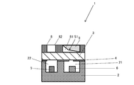
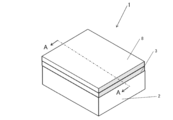
- FIG. 1 is a perspective view showing an optical sensor device according to a first embodiment of the present disclosure.
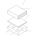
- 1 is an exploded perspective view showing an optical sensor device according to a first embodiment of the present disclosure. It is a sectional view showing an optical sensor device concerning a 1st embodiment of this indication.
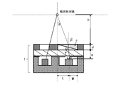
- FIG. 3 is a cross-sectional view showing parameters of the optical sensor device according to the first embodiment of the present disclosure.
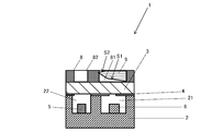
- FIG. 6 is a cross-sectional view showing an optical sensor device according to another mode related to the first embodiment of the present disclosure.
- FIG. 6 is a cross-sectional view showing an optical sensor device according to another mode related to the first embodiment of the present disclosure.
- FIG. 6 is a cross-sectional view showing an optical sensor device according to another mode related to the first embodiment of the present disclosure.
- FIG. 6 is a cross-sectional view showing an optical sensor device according to another mode related to the first embodiment of the present disclosure.
- FIG. 1 is a perspective view showing an optical sensor device according to a first embodiment of the present
- FIG. 6 is a cross-sectional view showing an optical sensor device according to another mode related to the first embodiment of the present disclosure.
- FIG. 6 is a cross-sectional view showing an optical sensor device according to another mode related to the first embodiment of the present disclosure.
- FIG. 6 is a cross-sectional view showing an optical sensor device according to another mode related to the first embodiment of the present disclosure.
- It is a perspective view showing an optical sensor device concerning a 2nd embodiment and a 3rd embodiment of this indication.
- It is an exploded perspective view showing an optical sensor device concerning a 2nd embodiment and a 3rd embodiment of this indication.
- It is sectional drawing which shows the optical sensor apparatus which concerns on 2nd Embodiment of this indication.
- FIG. 6 is a cross-sectional view showing an optical sensor device according to another mode related to the first embodiment of the present disclosure.
- FIG. 6 is a cross-sectional view showing an optical sensor device according to another mode related to the first embodiment of the present disclosure.
- It is a perspective view showing
- FIG. 11 is a cross-sectional view showing parameters of an optical sensor device according to another mode related to the second embodiment of the present disclosure. It is a top view showing an optical sensor device concerning a 2nd embodiment of this indication. It is a top view showing an optical sensor device concerning a 2nd embodiment of this indication. It is sectional drawing which shows the optical sensor apparatus which concerns on 3rd Embodiment of this indication. It is sectional drawing which shows the optical sensor apparatus which concerns on the other form concerning 3rd Embodiment of this indication. It is sectional drawing which shows the optical sensor apparatus which concerns on the other form concerning 3rd Embodiment of this indication. It is sectional drawing which shows the optical sensor apparatus which concerns on the other form concerning 3rd Embodiment of this indication. It is sectional drawing which shows the optical sensor apparatus which concerns on the other form concerning 3rd Embodiment of this indication. It is a top view showing an optical sensor device concerning a 3rd embodiment of this indication. It is a top view showing an optical sensor device concerning a 3rd
- the optical sensor device 1 includes a substrate 2, a first transparent substrate 3, a light shielding film 4, a light emitting element 5, a light receiving element 6, and a second transparent substrate 8.
- the substrate 2 has a rectangular shape in a plan view and may be formed by stacking a plurality of dielectric layers.
- the substrate 2 has, for example, a size of 0.5 mm to 5 mm and a thickness of 0.5 mm to 5 mm in plan view.
- the dielectric layer may be made of a ceramic material, and the dielectric layer may be made of an organic material.
- the substrate 2 is a wiring board made of a ceramic material (ceramic wiring board)
- conductors such as connection pads, internal wiring, and signal wiring are formed on the dielectric layer made of the ceramic material.
- Examples of the ceramic material used in the ceramic wiring board include an aluminum oxide sintered body, a mullite sintered body, a silicon carbide sintered body, an aluminum nitride sintered body, a silicon nitride sintered body, or a glass ceramic sintered body. Examples include ties.
- the substrate 2 is a wiring substrate made of an organic material (organic wiring substrate)
- a wiring conductor such as a signal wiring described later is formed on an insulating layer made of an organic material.
- the organic wiring board is formed of a plurality of organic dielectric layers.
- the organic wiring board may be, for example, a printed wiring board, a build-up wiring board, a flexible wiring board, or the like whose dielectric layer is made of an organic material.
- Examples of the organic material used in the organic wiring board include epoxy resin, polyimide resin, polyester resin, acrylic resin, phenol resin, and fluorine resin.
- the substrate 2 is provided with at least two recesses serving as openings.
- One of the two recesses is the first opening 21 for accommodating the light receiving element 6, and the one of the two recesses.
- the other is a second opening 22 that accommodates the light emitting element 5.
- the first opening 21 and the second opening 22 are provided so as to open on the same main surface (first surface of the substrate 2) 21 of the substrate 2.
- the optical sensor device 1 is preferably used as a measurement sensor that measures the flow of fluid such as blood flow by utilizing the Doppler effect of light.
- the measurement sensor includes a light emitting element 5 that irradiates the measured object with light, and a light receiving element 6 that receives the light scattered by the measured object.
- a part of the body such as a finger is irradiated with light from the outside, and light scattered by blood cells contained in blood flowing through blood vessels under the skin is received to obtain a frequency. Blood flow is measured from the change in.
- the light emitting element 5 and the light receiving element 6 are arranged at a predetermined interval based on the positional relationship between the irradiation light and the scattered light.
- the first opening 21 and the second opening 22 are provided according to the positional relationship with the light receiving element 6 and the light emitting element 5.
- the size of the first opening 21 and the size of the second opening 22 may be appropriately set according to the sizes of the light receiving element 6 and the light emitting element 5 to be housed.
- the light receiving element 6 and the light emitting element 5 are, for example, 0.1 mm ⁇ 0.1 mm ⁇ 0.1 mm to 1.5 mm ⁇ 1.5 mm ⁇ 1.2 mm.
- the opening of the second opening 22 may have, for example, a rectangular shape or a square shape, and its size.
- the shape of the opening of the first opening 21 may be rectangular or square.
- the size is, for example, 0.3 mm to 2.0 mm in length in the vertical direction, 0.3 mm to 2.0 mm in length in the horizontal direction, and depth is 0.4 mm to 1.5 mm.
- the distance between the first opening 21 and the second opening 22 (between the light receiving element 6 and the light emitting element 5) may be so large that the light emitted by the light emitting element 5 does not directly enter the light receiving element 6. ..
- the first opening 21 and the second opening 22 are provided.
- the light receiving element 6 and the light emitting element 5 can be made closer to each other. At this time, for example, when seen in a plan view, the center of the first opening portion 21 and the center of the light receiving element 6 overlap each other, and the center of the second opening portion 22 and the center of the light emitting element 5 overlap each other. May be.
- the opening shape of the first opening 21 and the second opening 22 may be, for example, a circular shape, a square shape, a rectangular shape, or any other shape. Further, the first opening 21 and the second opening 22 may have a uniform cross-sectional shape parallel to the main surface of the substrate 2 in the depth direction. It may be a concave portion having a step, which is the same as the opening shape and is uniform, and after the predetermined depth, the cross-sectional shape is small and the bottom is uniform.
- a mounting area for mounting the light receiving element 6 is provided on the bottom of the first opening 21, and a bottom of the second opening 22 is provided. A mounting area for mounting the light emitting element 5 is provided. Further, a connection pad for electrically connecting to the light emitting element 5 or the light receiving element 6 is provided on the step surface.
- the substrate 2 is provided with signal wiring electrically connected to the light emitting element 5 or the light receiving element 6, transmitting an electric signal input to the light emitting element 5, and transmitting an electric signal output from the light receiving element 6. It may be.
- the signal wiring is connected to the light emitting element 5 or the light receiving element 6 with a bonding wire which is a connecting member, a connection pad to which the bonding wire is connected, and an electrical connection to the connection pad from directly below the connection pad of the substrate 2. It may be composed of a via conductor extending to the lower surface (second surface of the substrate 2) and an external connection terminal electrically connected to the via conductor.
- the external connection terminal is provided on the lower surface of the substrate 2, and is electrically connected to the connection terminal of the external mounting substrate on which the measurement sensor including the optical sensor device 1 is mounted by a terminal connection material such as solder.
- the external connection terminals are, for example, a nickel layer having a thickness of 0.5 ⁇ m to 10 ⁇ m and a gold layer having a thickness of 0.5 ⁇ m to 5 ⁇ m in order to improve wettability with a bonding material such as solder and to improve corrosion resistance. And may be sequentially deposited by a plating method.
- the first transparent substrate 3 covers the upper surface of the substrate 2 (first surface of the substrate 2) and is bonded to the first surface of the substrate 2 with a bonding material.
- the first transparent substrate 3 closes and seals the first opening 21 and the second opening 22 in which the light receiving element 6 and the light emitting element 5 are accommodated.
- the first transparent substrate 3 is a plate-shaped member made of an insulating material, transmits light emitted from the light emitting element 5 accommodated in the second opening 22, and receives the light receiving element 6 accommodated in the first opening 21. It suffices that it is made of a material having a light-transmitting property such that the light received by is transmitted.
- a semiconductor laser element such as VCSEL can be used as the light emitting element 5, and various photodiodes such as a silicon photodiode, a GaAs photodiode, an InGaAs photodiode, and a germanium photodiode can be used as the light receiving element 6.
- the light emitting element 5 and the light receiving element 6 may be appropriately selected depending on the type of the object to be measured, the type of parameter to be measured, and the like.
- the VCSEL which is the light emitting element 5 can emit laser light having a wavelength of 850 nm in order to measure by utilizing the Doppler effect of light.
- the light emitting element 5 that emits laser light having a wavelength according to the purpose of measurement may be selected.
- the light receiving element 6 is only required to be able to receive the light emitted from the light emitting element 5 when the light to be received does not change in wavelength from the laser light emitted from the light emitting element 5, and when there is a change in wavelength, after the change. Any light can be received as long as it can receive light of the wavelength.
- the light emitting element 5 and the light receiving element 6 and the connection pad are electrically connected by, for example, the bonding wire 32, but flip chip connection, bump connection, connection using an anisotropic conductive film, and the like. Connection method may be used.
- the first transparent substrate 3 needs to transmit the irradiation light and the scattered light to the object to be measured. Since the characteristics of the irradiation light and the scattered light are determined by the mounted light emitting element, it is sufficient that at least the light emitted by the mounted light emitting element is transmitted.
- the first transparent substrate 3 may be made of an insulating material having a transmittance of 70% or more, preferably 90% or more of the light of the wavelength.
- the insulating material of the first transparent substrate 3 for example, a transparent ceramic material such as sapphire, a glass material, or a resin material can be used.
- a transparent ceramic material such as sapphire, a glass material, or a resin material
- the glass material borosilicate glass, crystallized glass, quartz, soda glass, or the like can be used.
- resin material polycarbonate resin, unsaturated polyester resin, epoxy resin or the like can be used.
- the first transparent substrate 3 has, for example, a rectangular shape in a plan view, and has a size of 0.5 mm ⁇ 1 mm to 5 mm ⁇ 5 mm. The thickness is 0.5 mm to 5 mm.
- the joining material joins the substrate 2 and the first transparent substrate 3 together. More specifically, the upper surface of the substrate 2 and the lower surface of the first transparent substrate 3 are joined at the outer peripheral portion.
- the bonding material is provided in a ring shape along the upper surface of the substrate 2, and is a sealing material for ensuring airtightness and watertightness in the first opening 21 and the second opening 22 of the substrate 2.
- the light-receiving element 6 and the light-emitting element 5 housed in the first opening 21 and the second opening 22 are vulnerable to moisture and the like, and the bonding material is seamless so as to prevent moisture from entering from the outside. It is provided in a ring shape.
- the bonding material may have a light shielding property. Since the bonding material has a light-shielding property, it is possible to reduce light entering from the outside through the space between the substrate 2 and the first transparent substrate 3 and into the first opening 21 and the second opening 22. Can be made
- the light blocking property of the bonding material may be a light blocking property due to absorption of light. From the viewpoint of preventing the entry of light from the outside, it may have a light-shielding property due to reflection, but stray light generated inside the measurement sensor may be reflected by the bonding material and further received by the light receiving element. .. If the bonding material absorbs light, it can absorb the light from the outside to prevent entry and also absorb the stray light generated inside.
- the bonding material is, for example, a resin-based adhesive such as an epoxy resin or a conductive silicone resin having a bonding property between the substrate 2 and the first transparent substrate 3 as a material having such a light blocking property by absorbing light. It is obtained by dispersing a light absorbing material.
- a light absorbing material for example, an inorganic pigment can be used.
- the inorganic pigment include carbon-based pigments such as carbon black, nitride-based pigments such as titanium black, Cr-Fe-Co-based, Cu-Co-Mn-based, Fe-Co-Mn-based, Fe-Co-Ni.
- a metal oxide pigment such as --Cr pigment can be used.
- the joining material may be made of a metal material such as solder.
- a brazing material such as Sn-Ag, Sn-Ag-Cu, Au-Sn, Au-Sn-Ag, Au-Si can be used.
- the light shielding film 4 may be provided on the lower surface of the first transparent substrate 3.
- the light shielding film 4 is made of, for example, a metal such as Cr, Ti, Al, Cu, Co, Ag, Au, Pd, Pt, Ru, Sn, Ta, Fe, In, Ni or W, or a metal material such as an alloy thereof. It is formed by vapor deposition, sputtering, baking or the like.
- the light-shielding film 4 has a thickness of, for example, 50 nm to 400 nm.
- the light shielding film 4 is located so as to overlap the light emitting element 5. At this time, overlapping means that the light shielding film 4 covers a part of the light emitting element 5.
- the light-shielding film 4 has a through hole in a part thereof so that at least the light emitted from the light emitting element 5 and the reflected light reaching the light receiving element 6 pass through.
- the light shielding film 4 may be located on the upper surface of the second transparent substrate 8 described later. It is possible to reduce the incidence of unnecessary scattered light on the light receiving element 6.
- the first through hole 81 has, for example, a circular shape or a rectangular shape, and has a size of ⁇ 50 ⁇ m to ⁇ 1 mm.
- the second through hole 82 has, for example, a circular shape or a rectangular shape, and has a size of ⁇ 5 ⁇ m to ⁇ 500 ⁇ m.
- the second transparent substrate 8 has the first through hole 81 at a position overlapping with the first opening 21. Further, the second transparent substrate 8 has a second through hole 82 at a position overlapping the second opening portion 22 with a space between the second transparent substrate 8 and the first through hole 81.
- the lens 9 is located in the first through hole 81.
- the second transparent substrate 8 is located on the upper surface of the first transparent substrate 3.
- a transparent ceramic material such as sapphire, a glass material, a resin material, or the like can be used.
- the glass material borosilicate glass, crystallized glass, quartz, soda glass, or the like can be used.
- a polycarbonate resin, an unsaturated polyester resin, an epoxy resin, or the like can be used, and the size thereof may be the same as that of the first transparent substrate 3 in plan view.
- the thickness may be one that considers the distance to the object.
- the lens 9 has a first inclined surface S1.
- the first inclined surface S1 is inclined downward from the light emitting element 5 side toward the light receiving element 6 side in a sectional view (inclined from left side to right side in FIG. 3).
- the first inclined surface S1 is inclined so as to approach the first transparent substrate 3 from the light emitting element 5 side toward the light receiving element 6 side. That is, the thickness of the lens increases from the inside of the substrate 2 toward the outside of the substrate 2.
- the cross-sectional view here is a cross section in the vertical direction of the optical device 1 and in a direction connecting the center of the light emitting element 5 and the center of the light receiving element 6.
- the optical sensor device 1 includes the lens 9 having the first inclined surface S1. Therefore, it is possible to make it easier to totally reflect the light (reference light) reflected on the surface of the object and to make the light (measurement light) reflected on the object more strongly incident on the light receiving element 6.
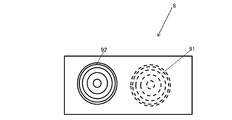
- the lower surface of the second transparent substrate 8 is a first diffractive lens having an uneven surface at a position overlapping the first opening 21 in plan view.
- concave portions and convex portions may be arranged concentrically alternately outward from the center, particularly from a position overlapping the light receiving element 6 in a plan view.
- the convex portion of the first diffractive lens 91 may have a third inclined surface S3 toward the center, and the inclination of the third inclined surface S3 with respect to the direction perpendicular to the thickness direction of the second transparent substrate 8. The angle may gradually increase.
- the tilt angle means a tilt angle with respect to a plane such as an upper surface and a lower surface of the second transparent substrate 8. That is, in plan view, only the convex portions, only the concave portions, or the convex portions and the concave portions are alternately arranged concentrically from the center toward the outside, and the distance between the convex portions and the concave portions is increased toward the outside. It may be narrowed. In the case of concentric circles, a spherical lens or the like can be used. It can also be manufactured by processing the surface by fine processing.
- the convex portion Since the convex portion is inclined, it is possible to make it difficult for reflected light other than the object and reflected light larger than the angle of reflection on the object to enter the light receiving element 6 at the third inclined surface S3. Alternatively, total reflection can be facilitated. Further, if it is concentric, it is possible to make it difficult for the reflected light having a larger angle than the reflection angle at the object to enter the light receiving element 6 or to facilitate total reflection regardless of the incident on the light receiving element 6 from any direction. it can.
- the reflected light refers to light reflected by the light emitted from the light emitting element 5 hitting an object or something other than the object.
- the upper surface of the second transparent substrate 8 may have a second diffractive lens 92 having an uneven surface at a position overlapping the second opening 22 in a plan view.
- the second diffractive lens 92 may have a convex portion of the second diffractive lens 92 that has a fourth inclined surface toward the center, and is the same as the light emitting element 5 in the center, particularly in plan view. From the overlapping position, only the convex portion, only the concave portion, or the convex portion and the concave portion may be alternately concentric to the outside. Further, the inclination angle of the fourth inclined surface may be larger than the thickness direction of the second transparent substrate 8 and the vertical direction.
- the optical sensor device 1 has the first diffractive lens 91 at a position overlapping the light receiving element 6, so that light other than the light to be measured, such as the reference light, can be totally reflected. it can.
- the condensing position of light other than the light to be measured, such as reference light can be prevented from overlapping the light receiving element 6.
- the size of the signal light incident on the light receiving element 6 can be relatively increased.
- the second transparent substrate 8 has a first region R1 and a second region R2, which have different refractive indexes, at positions overlapping the first opening 21 in plan view.
- the plurality of regions such as the first region R1 and the second region R2 include not only the plane but also the thickness direction.
- the first region R1 and the second region R2 may be concentric with the center of the plurality of regions, particularly from a position overlapping the light receiving element 6 in a plan view, toward the outside.
- a region having a different refractive index may be located outside the first region R1 and the second region R2.
- regions having different refractive indexes may be concentrically located.
- the first region R1 and the second region R2 have a lower surface smaller than an upper surface.
- the boundary between the first region R1 and the second region R2 is inclined, and the second transparent substrate 8 is opposite to the first region R1 of the second region R2 than the boundary between the first region R1 and the second region R2.
- the side boundary may have a larger inclination angle.
- the second transparent substrate 8 has a plurality of regions having different refractive indexes, and the plurality of regions may be arranged concentrically. That is, in a plan view from the lower surface, the plurality of regions may have concentric circles outward from the center of the region, and the width of the regions may become narrower toward the outside.
- a spherical lens or the like can be adhered and used as the second transparent substrate 8. It can also be manufactured by performing fine processing such as changing the refractive index with laser light. With the concentric circles, it is possible to make it difficult for the reflected light having a larger angle than the reflection angle at the object to enter the light receiving element 6 or to facilitate the total reflection regardless of the incident on the light receiving element 6 from any direction. ..
- the second transparent substrate 8 has a third region R3 and a fourth region R4, which have different refractive indexes, at a position overlapping with the second opening 22 in a plan view.
- the third region R3 and the fourth region R4 may have concentric circles outward from the center where the plurality of regions are located, particularly from the position where the third region R3 and the fourth region R4 overlap with the light emitting element 5 in plan view.
- the boundary between the third region R3 and the fourth region R4 is inclined so that the lower face is larger than the upper face, and the second transparent substrate 8 is the third region.
- the inclination angle may be larger at the boundary of the fourth region R4 on the side opposite to the third region R3 than at the boundary of R3 and the fourth region R4. That is, each of the regions may have a concentric shape from the center where the plurality of regions are located to the outside in a plan view from the upper surface, and the width thereof may become narrower toward the outside.
- a spherical lens or the like can be adhered and used. It can also be manufactured by performing fine processing such as changing the refractive index with laser light. With the concentric circles, it is possible to easily collect light from any direction from the light emitting element 5.
- the first region R1 and the second region R2 having different refractive indexes are provided at the position where the light receiving element 6 overlaps, the light to be measured, such as the reference light. Other light can be totally reflected.
- the condensing position of light other than the light to be measured, such as reference light can be prevented from overlapping the light receiving element 6. As a result, the size of the light incident on the light receiving element 6 can be relatively increased.
- the substrate 2 is manufactured in the same manner as the method for manufacturing a multilayer wiring board.
- the ceramic material is alumina
- a raw material powder such as alumina (Al 2 O 3 ), silica (SiO 2 ), calcia (CaO) or magnesia (MgO) is suitable.
- An organic solvent and a solvent are added and mixed to form a slurry, which is formed into a sheet by a known doctor blade method, calendar roll method, or the like to obtain a ceramic green sheet (hereinafter, also referred to as a green sheet).
- the green sheet is punched into a predetermined shape, and an organic solvent and a solvent are added to and mixed with raw material powder such as tungsten (W) and a glass material to form a metal paste, which is printed on the surface of the green sheet by a printing method such as screen printing.
- a printing method such as screen printing.
- the via conductor has a through hole formed in the green sheet, and the through hole is filled with the metal paste by screen printing or the like.
- the metallized layer to be the ground conductor or the like is formed on the outermost surface by the metal paste.
- a plurality of green sheets thus obtained are laminated, and the substrates 2 are manufactured by co-firing the green sheets at a temperature of about 1600 ° C.
- a first transparent substrate 3 is prepared by cutting a glass material into a predetermined shape by cutting, cutting, or the like.
- a light-shielding film 4 described later is formed by vapor deposition, sputtering, baking or the like.
- the via conductor is formed in a straight line in the vertical direction in the substrate 2, but if it is electrically connected from the upper surface of the substrate 2 to the external connection terminal on the lower surface, it is in a straight line.
- it may be formed so as to be displaced in the substrate 2 by an inner layer wiring, an internal ground conductor layer, or the like.
- the cutting process, the imprinting method using a die, or the like can be used, as in the method for manufacturing the first transparent substrate 3, the lens 9, and the like.
- the cutting process there are a method of directly processing a transparent substrate having a rectangular parallelepiped shape, and a method of embedding a separately manufactured lens or sloped glass in a base substrate on which holes have been drilled and fixing it with an adhesive or the like.
- the first inclined surface S1 of the lower surface of the lens 9 has an inclination angle that totally reflects reflected light larger than reflected light from the object. You may have. According to this configuration, it is possible to reduce the incidence of light other than the object and increase the light intensity of the reflected light from the object, so that more accurate measurement can be performed.
- the reflection angle is set to ⁇ 1, and when the target object is covered with the fluid, for example, the surface of a blood vessel or the like, is reflected.
- ⁇ is the ⁇ shown in FIG.
- the refractive index of the lens 9 may be larger than that of air.
- n1 is the refractive index of air
- n2 is the refractive index of the lens 9, and by increasing the refractive index of n2, total reflection can be made easier to occur.
- the respective parameters that can increase the intensity of the light to be measured using the symbols shown in FIG. 4 are as follows.
- h is the distance from the object to be reflected to the upper surface of the lens 9 having the first inclined surface S1
- d is the thickness of the second transparent substrate 8
- g is the distance from the lens 9 having the first inclined surface S1 to the light receiving portion.
- the distance, r is the half value of the width of the light receiving portion
- L is the horizontal distance from the object to be reflected to the center of the light receiving portion
- w is the horizontal distance from the right end of the lens 9 having the first inclined surface S1 to the light receiving point
- n is the first The refractive index of the lens 9 having the inclined surface S1 and ⁇ , ⁇ and ⁇ are angles.
- W ((L-htan ⁇ -dtan ⁇ ) (1-tan ⁇ tan ⁇ ) -gtan ⁇ (1-tan ⁇ tan ⁇ )) / under the condition of ⁇ > 0 °. (Tan ⁇ (tan ⁇ -tan ⁇ )).
- W1 ((L ⁇ r-htan ⁇ -dtan ⁇ ) (1-tan ⁇ tan ⁇ ) -gtan ⁇ (1-tan ⁇ tan ⁇ )) / (tan ⁇ (tan ⁇ -tan ⁇ )).
- the upper surface of the lens 9 may be inclined from the light emitting element 5 side toward the light receiving element 6 side in a sectional view. That is, the lens 9 may have the second inclined surface S2 on the upper surface. At this time, the second inclined surface S2 is inclined upward. This makes it easier to totally reflect the light.
- only a part of the upper surface of the lens 9 on the light emitting element 5 side may be tilted as shown in FIG. 5, or the entire surface is tilted. May be.
- the lower surface of the lens 9 may be inclined only on the light emitting element 5 side of the lower surface of the lens 9, or the entire surface of the lower surface of the lens 9 may be inclined. It may be inclined.
- the lens 9 may be vertically symmetrically inclined, and at that time, a part of the upper surface and the lower surface may be inclined.
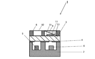
- an optical sensor device 1 is located on the upper surface of the first transparent substrate 3 at a position overlapping the first opening 21 and the first through hole 81, and at the same time, the lens
- the first condensing lens 11 may be attached below the unit 9.
- the first condenser lens 11 has, for example, a size of ⁇ 20 ⁇ m to ⁇ 2 mm and a thickness of 0.5 mm to 2 mm in plan view.
- the first condenser lens 11 is made of, for example, a glass material such as quartz glass or borosilicate glass, or a resin material such as acrylic, polycarbonate, styrene, or polyolefin.
- the first condenser lens 11 is preferably transparent so that the light emitted from the light emitting element 5 passes through the light receiving element 6.
- a condenser lens having a property of refracting light in the optical axis direction such as a convex lens.
- the presence of the first condensing lens 11 refracts diffused light, which is the light emitted from the light emitting element 5, to form focused light or collimator light, thereby improving the light converging property of the light on the light receiving element 6.
- the second condenser lens 12 may be further attached to the upper surface of the first transparent substrate 3 at a position overlapping the second opening 22 and the second through hole 82.
- the second condenser lens 12 has a size of, for example, ⁇ 70 ⁇ m to ⁇ 2 mm and a thickness of 50 ⁇ m to 2 mm in plan view.
- the second condenser lens 12 is made of, for example, a glass material such as quartz glass or borosilicate glass, or a resin material such as acrylic, polycarbonate, styrene, or polyolefin.
- the second condenser lens 12 is preferably transparent so as to allow the light emitted from the light emitting element 5 to pass therethrough.
- the second condenser lens 12 it is preferable to use a condenser lens or the like having a property of refracting light in the optical axis direction. Since the second condenser lens 12 is provided, the diffused light emitted from the light emitting element 5 is refracted to be focused light or collimated light, so that the light converging property can be improved.
- the optical sensor device 1 is used by being mounted on an external mounting board.
- an external mounting board for example, a control element for controlling the light emission of the light emitting element 5, an arithmetic element for calculating the blood flow velocity and the like from the output signal of the light receiving element 6, etc.
- the light emitting element control current from the external mounting substrate via the external connection terminal is the optical sensor device in a state where the fingertips of the fingers as the object to be measured (object) are in contact with the surface of the second transparent substrate 8. 1 is input to the light emitting element 5 through the via conductor, the connection pad, and the like, and the measurement light is emitted from the light emitting element 5.
- the emitted light passes through the first transparent substrate 3 and is applied to the fingertip, it is scattered by blood cells in the blood.
- the scattered light transmitted through the first transparent substrate 3 is received by the light receiving element 6, an electric signal according to the amount of received light is output from the light receiving element 6.
- the output signal passes through the connection pad and the via conductor, and is output from the optical sensor device 1 to the external mounting board via the external connection terminal.
- the signal output from the optical sensor device 1 is input to the arithmetic element, and the blood flow velocity is calculated by, for example, analyzing the intensity for each frequency of the scattered light received by the light receiving element 6.
- a space between the lower surface of the first transparent substrate 3 and the substrate 2 is provided between the first opening 21 and the second opening 22.
- the substrate 2 is in a state in which there is a light blocking wall between the first opening 21 and the second opening 22 and there is no part of the upper end of the wall.
- the optical sensor device 1 may include a first diffractive lens 91 that totally reflects reflected light having an incident angle larger than that of reflected light from an object.
- the first diffractive lens 91 may be provided so that at least the collection position of the reflected light having an incident angle larger than the reflected light from the object does not overlap the light receiving element 6. According to this configuration, it is possible to reduce the incidence of the light reflected from other than the target on the light receiving element 6, and it is possible to relatively increase the light intensity of the reflected light from the target, so that it is more accurate. Various measurements can be performed.
- first diffractive lens 91 and the second diffractive lens 92 may have the same shape, and as shown in FIG. 13, the shape and position of each lens may be the same on the upper surface and the lower surface. In such a case, processing becomes easy.
- the first diffractive lens 91 and the second diffractive lens 92 may have different shapes. At this time, they may have the same size or may have the same shape and have a similar relationship.
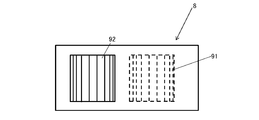
- the first diffractive lens 91 may have concave portions and convex portions arranged alternately from the center of the first diffractive lens 91 toward the outside. That is, as shown in FIG. 15, the first diffractive lens 91 may have a rectangular outer edge in plan view, and irregularities may be formed parallel to one side of the outer edge rectangle. Also in this case, similarly, the inclination angle of the third inclined surface S3 of the convex portion may increase as the distance from the position directly above the light receiving element 6 increases. That is, in a plan view, the interval between the concave portion, the convex portion, or the concave portion and the convex portion becomes narrower from the center of the first diffractive lens 91 toward the outside of the first diffractive lens 91. As a result, it is possible to make it difficult for incident light to the light receiving element 6 from any direction to enter the light receiving element 6 with reflected light larger than the reflection angle at the object.
- the second diffractive lens 92 may also be uneven from the center toward the outside. That is, the outer edge may have a rectangular shape in plan view, and may be uneven in parallel to one side of the rectangle. In this case as well, the inclination angle of the uneven third inclined surface S3 may increase as the distance from the position directly above the light emitting element 5 increases. That is, in plan view, the width of the unevenness becomes narrower from the center toward the outside.
- the optical sensor device 1 may be capable of totally reflecting reflected light having an incident angle larger than that of reflected light from an object.
- at least the condensing position of the reflected light having an incident angle larger than the reflected light from the object can be prevented from overlapping the light receiving element 6.
- the first region R1 and the third region R3, and the second region R2 and the fourth region R4 may have the same shape, or may be arranged symmetrically to each other. In such a case, processing becomes easy. Moreover, the first region R1 and the third region R3, and the second region R2 and the fourth region R4 may have different shapes.
- the first region R1 and the second region R2 may be located side by side from the center toward the outside. That is, as shown in FIG. 21, the outer edge may have a rectangular shape in a plan view and may be arranged parallel to one side of the rectangle. Further, the third region R3 and the fourth region R4 may also be located side by side from the center toward the outside.
- the refractive index of the second region R2 may be smaller than that of the first region R1. In this case, total reflection is likely to occur at the boundary surface between the first region R1 and the second region R2. Further, it is possible to easily reduce the incidence on the light receiving element 6.
- the present disclosure is not limited to the example of the above embodiment, and various modifications such as numerical values are possible. Further, the mounting method of each element in this embodiment is not specified. Further, the respective embodiments according to the present disclosure can be combined in all as long as the contents are not inconsistent. Further, although the optical sensor device according to the embodiment of the present disclosure has been described as its application as a pulse wave blood flow sensor device, other devices that operate by a pair of sensor elements of a light emitting element and a light receiving element, for example, a proximity illuminance integrated type It can be applied to a sensor device, a proximity sensor device, a distance measuring sensor device, and the like.
- Optical Sensor Device 2 Substrate 3 First Transparent Substrate 4 Light-Shielding Film 5 Light-Emitting Element 6 Light-Receiving Element 8 Second Transparent Substrate 9 Lens 21 First Opening 22 Second Opening 81 First Through Hole 82 Second Through Hole 11 First Condensing lens 12 Second condensing lens 91 First diffractive lens 92 Second diffractive lens R1 First region R2 Second region R3 Third region R4 Fourth region S1 First inclined surface S2 Second inclined surface S3 Third inclined surface
Landscapes
- Physics & Mathematics (AREA)
- Health & Medical Sciences (AREA)
- Life Sciences & Earth Sciences (AREA)
- General Physics & Mathematics (AREA)
- Optics & Photonics (AREA)
- Engineering & Computer Science (AREA)
- Molecular Biology (AREA)
- Cardiology (AREA)
- Physiology (AREA)
- Veterinary Medicine (AREA)
- Biophysics (AREA)
- Pathology (AREA)
- Public Health (AREA)
- Biomedical Technology (AREA)
- Heart & Thoracic Surgery (AREA)
- Medical Informatics (AREA)
- Hematology (AREA)
- Surgery (AREA)
- Animal Behavior & Ethology (AREA)
- General Health & Medical Sciences (AREA)
- Electromagnetism (AREA)
- Fluid Mechanics (AREA)
- Measuring Pulse, Heart Rate, Blood Pressure Or Blood Flow (AREA)
- Investigating Or Analysing Materials By Optical Means (AREA)
- Switches Operated By Changes In Physical Conditions (AREA)
- Photo Coupler, Interrupter, Optical-To-Optical Conversion Devices (AREA)
Abstract
光学センサ装置は、基板と、受光素子と、発光素子と、第1透明基板と、第2透明基板とを備えている。基板は、第1開口部と、第1開口部と間を空けて位置した第2開口部とを有する。受光素子は、第1開口部に位置している。発光素子は、第2開口部に位置するとともに、受光素子と間を空けて位置している。第1透明基板は、基板の上面に位置し、第1開口部および第2開口部を塞いで基板と接合されている。第2透明基板は、第1透明基板の上面に位置している。
Description
本開示は、光学センサ装置に関する。
血流等の生体情報あるいは半導体装置等を流れる流体の状態を簡単に、かつ高速に測定できる計測センサ等の光学センサ装置が求められている。例えば血流は、光のドップラー効果を利用して計測することができる。血液に光を照射すると、赤血球等の血球細胞で光が散乱される。照射光の周波数と散乱光の周波数とから血球細胞の移動速度が算出される。血流等を計測できる光学センサ装置は、例えば、特開2011-134463号公報(特許文献1)に開示されている。
しかしながら、特許文献1に開示された光学センサ装置では、例えば血液の場合、発光素子から発光された光が、少なくとも2つの物に当たって2つの光が反射される。対象物の1つは血管であり、もう1つは血液である。このとき、この2つの反射した光を受光素子で検知する際に、血管で反射した光の強度が強くなり、測定対象である血液で反射した光の強度が弱くなる可能性があった。
本開示の一実施形態に係る光学センサ装置は、基板と、受光素子と、発光素子と、第1透明基板と、第2透明基板とを備えている。基板は、第1開口部と、第1開口部と間を空けて位置した第2開口部とを有する。受光素子は、第1開口部に位置している。発光素子は、第2開口部に位置するとともに、受光素子と間を空けて位置している。第1透明基板は、基板の上面に位置し、第1開口部および第2開口部を塞いで基板と接合されている。第2透明基板は、第1透明基板の上面に位置している。
図1~図22において、光学センサ装置1は、基板2と、第1透明基板3と、遮光膜4と、発光素子5と、受光素子6と、第2透明基板8とを備えている。
基板2は、平面視において、矩形状であって、複数の誘電体層が積層されて形成されていてもよい。基板2は、例えば、平面視において、大きさが0.5mm~5mmであって、厚みが0.5mm~5mmである。基板2は、例えば誘電体層がセラミック材料からなっていてもよく、誘電体層が有機材料からなっていてもよい。
基板2が、セラミック材料による配線基板(セラミック配線基板)の場合、セラミック材料からなる誘電体層に接続パッド、内部配線、信号配線等の各導体が形成される。
セラミック配線基板で用いられるセラミック材料としては、例えば、酸化アルミニウム質焼結体、ムライト質焼結体、炭化珪素質焼結体、窒化アルミニウム質焼結体、窒化珪素質焼結体またはガラスセラミックス焼結体等が挙げられる。
また、基板2が、有機材料による配線基板(有機配線基板)の場合、有機材料からなる絶縁層に後述する信号配線等の配線導体が形成される。有機配線基板は、複数の有機誘電体層から形成される。有機配線基板は、例えば、プリント配線基板、ビルドアップ配線基板またはフレキシブル配線基板等の誘電体層が有機材料からなるものであればよい。有機配線基板で用いられる有機材料としては、例えば、エポキシ樹脂、ポリイミド樹脂、ポリエステル樹脂、アクリル樹脂、フェノール樹脂またはフッ素系樹脂等が挙げられる。
また、この基板2には、少なくとも2つの開口部となる凹部が設けられており、2つの凹部のうちの一方は、受光素子6を収容する第1開口部21であり、2つの凹部のうちの他方は、発光素子5を収容する第2開口部22である。第1開口部21および第2開口部22は、基板2の同一の主面(基板2の第1面)21に開口するように設けられている。
本開示の実施形態に係る光学センサ装置1は、光のドップラー効果を利用して、血流等の流体の流れを計測する計測センサに好適に用いられる。光のドップラー効果を利用するために、計測センサは、被計測物に光を照射する発光素子5と、被計測物によって散乱された光を受光する受光素子6とを備える。特に、血流を計測する場合には、例えば手指等の身体の一部に外部から光を照射し、皮膚下の血管を流れる血液に含まれる血球細胞によって散乱された光を受光して、周波数の変化から血流を測定する。そのため、光学センサ装置1においては、照射光と散乱光の位置関係に基づいて、発光素子5と受光素子6とを所定の間隔で配置する。第1開口部21および第2開口部22は、受光素子6および発光素子5との位置関係に応じて設けられる。
第1開口部21の大きさ、第2開口部22の大きさは、収容しようとする受光素子6および発光素子5の大きさに応じて適宜設定すればよい。受光素子6および発光素子5は、例えば、0.1mm×0.1mm×0.1mm~1.5mm×1.5mm×1.2mmである。例えば、発光素子5として、垂直共振器面発光レーザ素子(VCSEL)を用いる場合、第2開口部22の開口は、その形状が、例えば矩形であっても正方形であってもよく、その大きさは、例えば、縦方向長さが0.3mm~2.0mm、横方向長さが0.3mm~2.0mmであり、深さは、0.3mm~1.0mmである。また、LED(Light emitting Diode)また、受光素子6として、面入射フォトダイオードを用いる場合、第1開口部21の開口は、その形状が、例えば矩形であっても正方形であってもよく、その大きさは、例えば、縦方向長さが0.3mm~2.0mm、横方向長さが0.3mm~2.0mmであり、深さは、0.4mm~1.5mmである。第1開口部21と第2開口部22との間(受光素子6と発光素子5との間)は、発光素子5が発光した光が受光素子6に直接入射しない程度に離れていればよい。また、第1開口部21と第2開口部22との間(受光素子6と発光素子5との間)に遮光性のある壁を設けることで、第1開口部21と第2開口部22との間(受光素子6と発光素子5との間)の距離を近づけることができる。このとき、例えば、平面透視において、第1開口部21の中心と受光素子6の中心とが重なって位置しており、第2開口部22の中心と発光素子5の中心とが重なって位置していてもよい。
第1開口部21および第2開口部22は、開口形状が、例えば、円形状、正方形状、矩形状等であってもよく、その他の形状であってもよい。また、第1開口部21および第2開口部22は、基板2の主面に平行な断面形状が深さ方向に一様な形状であってもよいが、所定の深さまでは、断面形状が開口形状と同じで一様であり、所定の深さ以降は、断面形状が小さくなって底部まで一様であるような、段差付きの凹部であってもよい。本開示の一実施形態のように段差付きの凹部である場合は、第1開口部21の底部に、受光素子6を実装するための実装領域が設けられ、第2開口部22の底部に、発光素子5を実装するための実装領域が設けられる。また、段差表面には、発光素子5または受光素子6と電気的に接続するための接続パッドが設けられる。
また、基板2には、発光素子5または受光素子6と電気的に接続され、発光素子5に入力される電気信号が伝送され、受光素子6から出力される電気信号が伝送される信号配線があってもよい。この信号配線は、発光素子5または受光素子6と接続する接続部材であるボンディングワイヤと、ボンディングワイヤが接続される接続パッドと、接続パッドに電気的に接続して接続パッドの直下から基板2の下面(基板2の第2面)にまで延びるビア導体と、ビア導体に電気的に接続する外部接続端子とからなっていてもよい。外部接続端子は、基板2の下面に設けられており、光学センサ装置1を備える計測センサが実装される外部実装基板の接続端子とはんだ等の端子接続材料によって電気的に接続される。
外部接続端子は、はんだ等の接合材との濡れ性を向上させ、耐食性を向上させるために、例えば、厚さが0.5μm~10μmのニッケル層と厚さが0.5μm~5μmの金層とをめっき法によって順次被着させてもよい。
第1透明基板3は、基板2の上面(基板2の第1面)を覆い、接合材によって基板2の第1面に接合される。第1透明基板3によって、受光素子6および発光素子5が収容された第1開口部21および第2開口部22が塞がれて封止される。第1透明基板3は、絶縁材料からなる板状部材であり、第2開口部22に収容される発光素子5から出射される光が透過し、第1開口部21に収容される受光素子6が受光する光が透過するような光透過性を有する材料で構成されていればよい。
発光素子5は、VCSEL等の半導体レーザ素子を用いることができ、受光素子6は、シリコンフォトダイオード、GaAsフォトダイオード、InGaAsフォトダイオード、ゲルマニウムフォトダイオード等の各種フォトダイオードを用いることができる。発光素子5および受光素子6は、被計測物の種類、計測するパラメータの種類等により適宜選択すればよい。
血流を測定する場合は、例えば、光のドップラー効果を利用して測定するために、発光素子5であるVCSELとして波長が850nmのレーザ光を出射可能なものであればよい。その他の測定を行う場合は、測定目的に応じた波長のレーザ光を出射する発光素子5を選択すればよい。受光素子6は、受光する光が発光素子5から出射されるレーザ光から波長の変化が無い場合、発光素子5の出射光を受光できるものであればよく、波長の変化が有る場合、変化後の波長の光を受光できるものであればよい。
発光素子5および受光素子6と接続パッドとは、本実施形態では、例えば、ボンディングワイヤ32によって電気的に接続されるが、フリップチップ接続、バンプ接続、異方性導電フィルムを用いた接続等他の接続方法であってもよい。
また、第1透明基板3は、被計測物への照射光および散乱光を透過する必要がある。照射光および散乱光の特性は、搭載する発光素子によって決まるので、少なくとも搭載する発光素子が出射する光が透過するように構成されていればよい。発光素子から出射される光の波長に対して、当該波長の光の透過率が70%以上、好ましくは90%以上の透過率を有する絶縁材料で第1透明基板3を構成すればよい。
第1透明基板3は、絶縁材料としては、例えばサファイア等の透明セラミック材料、ガラス材料または樹脂材料等を用いることができる。ガラス材料としては、ホウケイ酸ガラス、結晶化ガラス、石英、ソーダガラス等を用いることができる。樹脂材料としては、ポリカーボネート樹脂、不飽和ポリエステル樹脂、エポキシ樹脂等を用いることができる。また、第1透明基板3は、平面視において、例えば矩形状であり、大きさは0.5mm×1mm~5mm×5mmである。また、厚みは、0.5mm~5mmである。
また接合材は、基板2と第1透明基板3とを接合する。より詳細には、基板2の上面と第1透明基板3の下面とを、外周部分で接合する。接合材は、基板2の上面に沿って環状に設けられており、基板2の第1開口部21および第2開口部22内の気密性および水密性を確保するためのシール材である。第1開口部21および第2開口部22に収容される受光素子6および発光素子5は、いずれも水分等に弱く、外部からの水分の進入を防止するために、接合材は、途切れの無い環状に設けられる。
さらに、接合材は遮光性を有していてもよい。接合材が遮光性を有することで、外部からの光が、基板2と第1透明基板3との間を通って、第1開口部21内、第2開口部22内に進入することを低減させることができる。
接合材が有する遮光性は、光の吸収による遮光性であってもよい。外部からの光の進入を防ぐ観点からは、反射による遮光性であってもよいが、計測センサの内部で発生した迷光が、接合材で反射してさらに受光素子に受光されてしまうおそれがある。接合材が光を吸収するものであれば、外部からの光を吸収して進入を防ぐとともに、内部で発生した迷光も吸収することができる。
接合材は、このような光の吸収による遮光性を有する材料としては、例えば、基板2と第1透明基板3との接合性を有するエポキシ樹脂、導電性シリコン樹脂等の樹脂系接着剤に、光吸収性材料を分散させて得られる。光吸収材料としては、例えば、無機顔料を用いることができる。無機顔料としては、例えば、カーボンブラックなどの炭素系顔料、チタンブラックなどの窒化物系顔料、Cr-Fe-Co系、Cu-Co-Mn系、Fe-Co-Mn系、Fe-Co-Ni-Cr系などの金属酸化物系顔料等を用いることができる。また、接合材は、はんだなどの金属材料で構成されていてもよい。例えば、Sn-Ag、Sn-Ag-Cu、Au-Sn、Au-Sn-Ag、Au-Siなどのろう材を用いることができる。
第1透明基板3の下面において遮光膜4を有していてもよい。遮光膜4は、例えば、Cr、Ti、Al、Cu、Co、Ag、Au、Pd、Pt、Ru、Sn、Ta、Fe、In、Ni若しくはWなどの金属又はこれらの合金等の金属材料を蒸着、スパッタ、焼付け等によって形成される。遮光膜4の厚みは、例えば、50nm~400nmである。遮光膜4は、発光素子5と重なって位置している。このとき、重なっているとは、遮光膜4が発光素子5の一部を覆っている状態のことを指す。遮光膜4は、少なくとも発光素子5が発光した光および受光素子6まで届く反射した光が通るように、一部に貫通孔がある。遮光膜4は、後述する第2透明基板8の上面に位置していてもよい。不要な散乱光が受光素子6に入射されることを低減させることができる。
遮光膜4において、第1貫通孔81は、例えば、円形状、矩形状であり、大きさがΦ50μm~Φ1mmである。また、第2貫通孔82は、例えば、円形状、矩形状であり、大きさがΦ5μm~Φ500μmである。本開示の第1実施形態においては、第2透明基板8は、第1開口部21と重なる位置に第1貫通孔81を有している。また、第2透明基板8は、第1貫通孔81と間を空けて、第2開口部22と重なる位置に第2貫通孔82を有している。第1貫通孔81には、レンズ9が位置している。
第1透明基板3の上面には、第2透明基板8が位置している。第2透明基板8は、例えば、サファイア等の透明セラミック材料、ガラス材料または樹脂材料等を用いることができる。ガラス材料としては、ホウケイ酸ガラス、結晶化ガラス、石英、ソーダガラス等を用いることができる。樹脂材料としては、ポリカーボネート樹脂、不飽和ポリエステル樹脂、エポキシ樹脂等を用いることができるまた、大きさは、平面視において、第1透明基板3と同じ大きさであってもよい。厚みは、対象物との距離を考慮したものであればよい。
レンズ9は、第1傾斜面S1を有している。第1傾斜面S1は、断面視において、発光素子5側から受光素子6側に向かって下方に傾斜している(図3において左側から右側へ傾斜)。換言すれば、断面視において、第1傾斜面S1は、発光素子5側から受光素子6側に向かうにつれて、第1透明基板3に近づくように傾斜している。つまり、基板2の内側から基板2の外側に向かってレンズの厚みが厚くなっている。なお、ここでいう、断面視とは、光学装置1を上下方向に、かつ、発光素子5の中心と受光素子6の中心とを結ぶ方向での断面のことである。
本開示の実施形態に係る光学センサ装置1では、第1傾斜面S1を有するレンズ9を備えている。そのため、対象物の表面に当たって反射した光(参照光)を全反射させやすくするとともに、対象物に当たって反射した光(測定光)をより強く受光素子6に入射させやすくすることができる。
本開示の第2実施形態においては、図13および図14に示すように、第2透明基板8の下面は、平面視において第1開口部21と重なる位置に、表面が凹凸の第1回折レンズ91を有している。第1回折レンズ91は、中心、特に平面視において受光素子6と重なる位置から、外側に向かって凹部分と凸部分が交互に同心円状に並んでいてもよい。また、第1回折レンズ91の凸部分は中心に向かう第3傾斜面S3を有していてもよく、第2透明基板8の厚み方向に垂直な方向に対してその第3傾斜面S3の傾斜角度が徐々に大きくなっていってもよい。このとき、傾斜角度は第2透明基板8の上面および下面等の平面に対する傾斜の角度のことである。つまり、平面視において、中心から外側に向かって凸部分のみ、凹部分のみあるいは、凸部分および凹部分が交互に同心円状に並んでおり、凸部分および凹部分の間隔が、外側に向かうに連れて狭くなっていてもよい。同心円状の場合には、球面レンズ等を用いることができる。また、微細加工にて表面を加工することでも作製できる。凸部分が傾斜していることによって、第3傾斜面S3で、対象物以外の反射光および対象物での反射角度よりも大きい反射光を受光素子6に入り難くすることができる。または、全反射させやすくすることができる。さらに同心円状であれば、どの方向からの受光素子6への入射に対しても、対象物での反射角度よりも大きい反射光を受光素子6に入り難くする、または全反射させやすくすることができる。反射光とは、対象物あるいは対象物以外の何かに発光素子5から発光した光が当たって反射した光のことをいう。
また、第2透明基板8の上面は、平面視において第2開口部22と重なる位置に、表面が凹凸の第2回折レンズ92を有していてもよい。第2回折レンズ92は、第1回折レンズ91と同様に、第2回折レンズ92の凸部分は中心に向かう第4傾斜面を有していてもよく、中心、特に平面視において発光素子5と重なる位置から、外側に向かって凸部分のみ、凹部分のみあるいは、凸部分および凹部分が交互に同心円状になっていてもよい。また、第2透明基板8の厚み方向、垂直な方向に対してその第4傾斜面の傾斜角度が大きくなっていってもよい。つまり、平面視において、中心から外側に向かって、凸部分のみ、凹部分のみあるいは、凸部分および凹部分が交互に同心円状になっており、凸部分および凹部分の間隔が、外側に向かうに連れて狭くなっていてもよい。同心円状の場合には、球面レンズ等を用いることができる。また、微細加工にて表面を加工することでも作製できる。凸部分が傾斜していることによって、第4傾斜面で集光させて発光素子5からの光を対象物に集中して当てやすくすることができる。さらに同心円状であれば、どの方向からの発光素子5からの入射に対しても、集光させやすくすることができる。
本開示の実施形態に係る光学センサ装置1では、受光素子6と重なる位置に第1回折レンズ91を有していることによって、参照光等の、計測したい光以外の光を全反射することができる。または、参照光等の、計測したい光以外の光の集光位置を受光素子6と重ならないようにすることができる。この結果、受光素子6に入射される信号光の大きさを相対的に大きくすることができる。
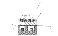
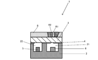
本開示の第3実施形態に係る発明は、第2透明基板8は、平面視において第1開口部21と重なる位置に、屈折率が互いに異なる第1領域R1および第2領域R2を有する。なお、第1領域R1、第2領域R2等の複数の領域は、平面だけでなく、厚み方向も含めたものである。平面視において、第1領域R1および第2領域R2は順に、複数の領域の中心、特に平面視において受光素子6と重なる位置から、外側に向かって同心円状になっていてもよい。このとき、第1領域R1および第2領域R2よりも外側にさらに屈折率の異なる領域が位置していてもよい。さらに平面視における第1開口部21と重なる位置において、屈折率が互いに異なる領域が同心円状に位置していてもよい。また、受光素子6と発光素子5の中心を結ぶ方向で、かつ、光学センサ装置1の上下方向における断面視において、第1領域R1および第2領域R2は、上面よりも下面が小さくなるように、第1領域R1および第2領域R2の境界が傾斜しており、第2透明基板8は、第1領域R1と第2領域R2との境界よりも第2領域R2の第1領域R1と反対側の境界の方が、傾斜角度が大きくなっていってもよい。第2透明基板8は、異なる屈折率の複数の領域を有しており、複数の領域が同心円状に並んでいてもよい。つまり、下面からの平面視において、複数の領域が位置する中心から外側に向かって同心円状になっており、領域の幅が、外側に向かうに連れて狭くなっていてもよい。同心円状の場合には、第2透明基板8としては、球面レンズ等を接着して用いることができる。また、レーザ光で屈折率を変化させる等の微細加工にて加工することでも作製できる。同心円状であれば、どの方向からの受光素子6への入射に対しても、対象物での反射角度よりも大きい反射光を受光素子6に入り難くする、または全反射させやすくすることができる。
また、第2透明基板8は、平面視において第2開口部22と重なる位置に、屈折率が互いに異なる第3領域R3および第4領域R4を有する。第3領域R3および第4領域R4は順に、複数の領域が位置する中心、特に平面視において発光素子5と重なる位置から、外側に向かって同心円状になっていてもよい。また、第3領域R3および第4領域R4は、上面よりも下面が大きくなるように、第3領域R3および第4領域R4の境界が傾斜しており、第2透明基板8は、第3領域R3と第4領域R4との境界よりも第4領域R4の第3領域R3と反対側の境界の方が、傾斜角度が大きくなっていってもよい。つまり、各領域は、上面からの平面視において、複数領域が位置する中心から外側に向かって同心円状になっており、その幅が、外側に向かうに連れて狭くなっていてもよい。同心円状の場合には、球面レンズ等を接着して用いることができる。また、レーザ光で屈折率を変化させる等の微細加工にて加工することでも作製できる。同心円状であれば、どの方向からの発光素子5からの入射に対しても、集光させやすくすることができる。
本開示の実施形態に係る光学センサ装置1では、受光素子6と重なる位置に屈折率が互いに異なる第1領域R1および第2領域R2を有していることによって、参照光等の、計測したい光以外の光を全反射させることができる。または、参照光等の、計測したい光以外の光の集光位置を受光素子6と重ならないようにすることができる。この結果、受光素子6に入射される光の大きさを相対的に大きくすることができる。
<光学センサ装置の製造方法>
光学センサ装置1の製造方法について説明する。まず、基板2を多層配線基板の製造方法と同様にして作製する。基板2が、セラミック配線基板であり、セラミック材料がアルミナである場合は、まずアルミナ(Al2O3)やシリカ(SiO2)、カルシア(CaO)、マグネシア(MgO)等の原料粉末に適当な有機溶剤、溶媒を添加混合して泥漿状とし、これを周知のドクターブレード法やカレンダーロール法等によってシート状に成形してセラミックグリーンシート(以下、グリーンシートともいう)を得る。その後、グリーンシートを所定形状に打ち抜き加工するとともに、タングステン(W)とガラス材料等の原料粉末に有機溶剤、溶媒を添加混合して金属ペーストとし、これをグリーンシート表面にスクリーン印刷等の印刷法でパターン印刷する。また、ビア導体は、グリーンシートに貫通孔を設け、スクリーン印刷等によって金属ペーストを貫通孔に充填させる。また、接地導体等となるメタライズ層は、金属ペーストによって最表面に形成される。こうして得られたグリーンシートを複数枚積層し、これを約1600℃の温度で同時焼成することによって基板2が作製される。
光学センサ装置1の製造方法について説明する。まず、基板2を多層配線基板の製造方法と同様にして作製する。基板2が、セラミック配線基板であり、セラミック材料がアルミナである場合は、まずアルミナ(Al2O3)やシリカ(SiO2)、カルシア(CaO)、マグネシア(MgO)等の原料粉末に適当な有機溶剤、溶媒を添加混合して泥漿状とし、これを周知のドクターブレード法やカレンダーロール法等によってシート状に成形してセラミックグリーンシート(以下、グリーンシートともいう)を得る。その後、グリーンシートを所定形状に打ち抜き加工するとともに、タングステン(W)とガラス材料等の原料粉末に有機溶剤、溶媒を添加混合して金属ペーストとし、これをグリーンシート表面にスクリーン印刷等の印刷法でパターン印刷する。また、ビア導体は、グリーンシートに貫通孔を設け、スクリーン印刷等によって金属ペーストを貫通孔に充填させる。また、接地導体等となるメタライズ層は、金属ペーストによって最表面に形成される。こうして得られたグリーンシートを複数枚積層し、これを約1600℃の温度で同時焼成することによって基板2が作製される。
一方、ガラス材料を、切削、切断等により所定の形状に切り出した第1透明基板3を準備する。第1透明基板3の下面に、蒸着、スパッタ、焼付け等によって後述する遮光膜4を形成する。
なお、上記では、ビア導体は、基板2内で上下方向に一直線状に形成される構成としているが、基板2の上面から下面の外部接続端子まで電気的に接続されていれば、一直線状でなく、基板2内で、内層配線や内部接地導体層等によってずれて形成されていてもよい。
第2透明基板8は、第1透明基板3及びレンズ9等の製造方法と同様に、切削加工、金型を用いたインプリント工法等を用いることができる。例えば、切削加工では直方体状の透明の基板を直接加工する方法と、穴あけ加工を行なった母体の基板に別体で作製したレンズや斜面状ガラスを埋め込んで接着材等で固定する方法である。
<光学センサ装置の第1実施形態に関わる他の形態>
本開示の他の実施形態に係る光学センサ装置1は、後述するように、レンズ9の下面の第1傾斜面S1は、対象物からの反射光よりも大きい反射光を全反射する傾斜角度を有していてもよい。この構成によれば、対象物以外の光が入射することを低減させることができ、対象物からの反射光の光強度を大きくすることができるため、より正確な測定を行なうことができる。
本開示の他の実施形態に係る光学センサ装置1は、後述するように、レンズ9の下面の第1傾斜面S1は、対象物からの反射光よりも大きい反射光を全反射する傾斜角度を有していてもよい。この構成によれば、対象物以外の光が入射することを低減させることができ、対象物からの反射光の光強度を大きくすることができるため、より正確な測定を行なうことができる。
具体的には、発光素子5から発光した光が対象物である流体、例えば血液等に当たって反射する際の反射角をθ1とし、対象物の流体を覆う物体、例えば血管等の表面に当たって反射する際の反射角をθ2とした場合に、
条件1 α≧sin-1(n1/n2)-sin-1(n1/n2*sinθ2)=α2
条件2 α<sin-1(n1/n2)-sin-1(n1/n2*sinθ1)=α1
とすると、α2≦α<α1であればよい。なお、αは、図4に示したαのことである。
条件1 α≧sin-1(n1/n2)-sin-1(n1/n2*sinθ2)=α2
条件2 α<sin-1(n1/n2)-sin-1(n1/n2*sinθ1)=α1
とすると、α2≦α<α1であればよい。なお、αは、図4に示したαのことである。
また、レンズ9の屈折率は、空気の屈折率よりも大きくてもよい。これは、先程の式に当てはめると、n1が空気の屈折率で、n2がレンズ9の屈折率であり、n2の屈折率を大きくすることで、より全反射を起きやすくさせることができる。
また、図4に示す符号を用いて、測定したい光の強度を大きくすることができるそれぞれのパラメータとしては、以下の通りである。なお、hは被反射物から第1傾斜面S1を有するレンズ9の上面までの距離、dは第2透明基板8の厚み、gは、第1傾斜面S1を有するレンズ9から受光部までの距離、rは受光部幅の半値、Lは被反射物からの受光部中心までの水平距離、wは第1傾斜面S1を有するレンズ9の右端から受光点までの水平距離、nは第1傾斜面S1を有するレンズ9の屈折率、そしてθ、β、γはそれぞれ角度である。このとき、距離Lの位置で受光する場合のWは、α>0°の条件のもとでは、W=((L-htanθ-dtanβ)(1-tanαtanγ)-gtanγ(1-tanαtanβ))/(tanα(tanγ-tanβ))である。左端、右端では、W1=((L±r-htanθ-dtanβ)(1-tanαtanγ)-gtanγ(1-tanαtanβ))/(tanα(tanγ-tanβ))になる。
また、レンズ9は、断面視において、上面も発光素子5側から受光素子6側に向かって傾斜していてもよい。つまり、レンズ9は、上面に第2傾斜面S2を有していてもよい。このとき、第2傾斜面S2は、上方に向かって傾斜している。このことによって、より全反射させやすくすることができる。
このとき、参照光のみを全反射しやすくするために、レンズ9の上面のうち、図5に示すように発光素子5側の一部のみを傾斜させていてもよいし、全体が傾斜していてもよい。
また、レンズ9の下面の傾斜も同様に、参照光のみを全反射しやすくするために、レンズ9の下面のうち、発光素子5側の一部のみを傾斜させていてもよいし、全体が傾斜していてもよい。
また、レンズ9は、上下対称に傾斜していてもよく、その際に、上面および下面の一部が傾斜していてもよい。
<光学センサ装置の第1実施形態に関わる他の形態>
図8に示すように、本開示の他の実施形態に係る光学センサ装置1は、第1透明基板3の上面において、第1開口部21および第1貫通孔81と重なる位置であるとともに、レンズ9の下方には、第1集光レンズ11が取付けられていてもよい。第1集光レンズ11は、平面視において、例えば、大きさがΦ20μm~Φ2mmの、厚みは0.5mm~2mmである。また、第1集光レンズ11は、例えば、石英ガラス、ホウケイ酸ガラスなどのガラス材料、アクリル、ポリカーボネート、スチレン、ポリオレフィンなどの樹脂材料から成っている。第1集光レンズ11は、発光素子5から放射された光を受光素子6に通すために透過性を有しているのがよい。また、第1集光レンズ11は、集光性を有する、凸レンズ等の光を光軸方向に屈折させる性質をもつものを用いるのがよい。第1集光レンズ11があることによって、発光素子5から照射された光である拡散光を屈折させ、集束光やコリメータ光にすることで受光素子6への光の集光性を向上させることができる。
図8に示すように、本開示の他の実施形態に係る光学センサ装置1は、第1透明基板3の上面において、第1開口部21および第1貫通孔81と重なる位置であるとともに、レンズ9の下方には、第1集光レンズ11が取付けられていてもよい。第1集光レンズ11は、平面視において、例えば、大きさがΦ20μm~Φ2mmの、厚みは0.5mm~2mmである。また、第1集光レンズ11は、例えば、石英ガラス、ホウケイ酸ガラスなどのガラス材料、アクリル、ポリカーボネート、スチレン、ポリオレフィンなどの樹脂材料から成っている。第1集光レンズ11は、発光素子5から放射された光を受光素子6に通すために透過性を有しているのがよい。また、第1集光レンズ11は、集光性を有する、凸レンズ等の光を光軸方向に屈折させる性質をもつものを用いるのがよい。第1集光レンズ11があることによって、発光素子5から照射された光である拡散光を屈折させ、集束光やコリメータ光にすることで受光素子6への光の集光性を向上させることができる。
このとき、第1透明基板3の上面において、第2開口部22および第2貫通孔82と重なる位置に、さらに第2集光レンズ12が取付けられていてもよい。第2集光レンズ12は、平面視において、例えば、大きさがΦ70μm~Φ2mmの、厚みは50μm~2mmである。また、第2集光レンズ12は、例えば、石英ガラス、ホウケイ酸ガラスなどのガラス材料、アクリル、ポリカーボネート、スチレン、ポリオレフィンなどの樹脂材料から成っている。第2集光レンズ12は、発光素子5から放射された光を通すために透過性を有しているのがよい。また、第2集光レンズ12は、集光性を有する、凸レンズ等の光を光軸方向に屈折させる性質をもつものを用いるのがよい。第2集光レンズ12があることによって、発光素子5から照射された拡散光を屈折させ、集束光やコリメータ光にすることで光の集光性を向上させることができる。
光学センサ装置1は、外部実装基板に実装されて使用される。外部実装基板には、例えば、発光素子5の発光を制御する制御素子、受光素子6の出力信号から血流速度等を算出する演算素子等も実装される。
測定する場合には、被計測物(対象物)として手指の指先を第2透明基板8の表面に接触させた状態で、外部実装基板から外部接続端子を介して発光素子制御電流が光学センサ装置1に入力され、ビア導体、接続パッド等を通って発光素子5に入力されて発光素子5から計測用の光が出射される。出射された光が、第1透明基板3を透過して指先に照射されると、血液中の血球細胞で散乱される。第1透明基板3を透過した散乱光が、受光素子6で受光されると、受光量に応じた電気信号が受光素子6から出力される。出力された信号は、接続パッド、ビア導体を通り、外部接続端子を介して光学センサ装置1から外部実装基板へと出力される。
外部実装基板では、光学センサ装置1から出力された信号が、演算素子に入力され、例えば、受光素子6が受光した散乱光の周波数毎の強度を解析することにより、血流速度を算出することができる。
また、本開示の他の実施形態に係る光学センサ装置1は、第1開口部21と第2開口部22との間において、第1透明基板3の下面と基板2との間が空いていてもよい。つまり、基板2は、第1開口部21と第2開口部22との間に遮光性を有する壁があり、その壁の上端の一部が無い状態のことをいう。このようにすることで、参照光を直接的に受光素子6に到達させることができるため、より正確な計測を実現することができる。
<光学センサ装置の第2実施形態に関わる他の形態>
本開示の他の実施形態に係る光学センサ装置1は、対象物からの反射光よりも入射角が大きい反射光を全反射する第1回折レンズ91を有していてもよい。または、少なくとも対象物からの反射光よりも入射角が大きい反射光の集光位置を受光素子6と重ならないようにすることができる第1回折レンズ91を有していてもよい。この構成によれば、対象物以外で反射した光が受光素子6に入射することを低減させることができ、対象物からの反射光の光強度を相対的に大きくすることができるため、より正確な測定を行なうことができる。
本開示の他の実施形態に係る光学センサ装置1は、対象物からの反射光よりも入射角が大きい反射光を全反射する第1回折レンズ91を有していてもよい。または、少なくとも対象物からの反射光よりも入射角が大きい反射光の集光位置を受光素子6と重ならないようにすることができる第1回折レンズ91を有していてもよい。この構成によれば、対象物以外で反射した光が受光素子6に入射することを低減させることができ、対象物からの反射光の光強度を相対的に大きくすることができるため、より正確な測定を行なうことができる。
また、第1回折レンズ91および第2回折レンズ92を同じ形状にしてもよく、また、図13に示すように、上面および下面において各レンズの形状および位置を同じにしてもよい。このような場合には、加工が容易になる。また、第1回折レンズ91および第2回折レンズ92は、異なる形状であってもよい。このとき、同じ大きさであってもよいし、形状が同じで相似の関係にあってもよい。
また、第1回折レンズ91は、第1回折レンズ91の中心から外側に向かって凹部分および凸部分が交互に並んでいてもよい。つまり、図15に示すように、平面視において、第1回折レンズ91は、外縁が矩形状であり、外縁の矩形の1辺に平行に凹凸が形成されていてもよい。この場合にも同様に、受光素子6の直上から離れていくにつれて、凸部分の第3傾斜面S3の傾斜角度が大きくなってもよい。つまり、平面視において、凹部分、凸部分または凹部分および凸部分の間隔が第1回折レンズ91の中心から第1回折レンズ91の外側に向かうに連れて狭くなっている。このことによって、どの方向からの受光素子6への入射に対しても、対象物での反射角度よりも大きい反射光を受光素子6に入り難くすることができる。
第1回折レンズ91と同様に、第2回折レンズ92も、中心から外側に向かって並んで凹凸になっていてもよい。つまり、平面視において、外縁が矩形状であり、矩形の1辺に平行に凹凸になっていてもよい。この場合にも同様に、発光素子5の直上から離れていくにつれて、凹凸の第3傾斜面S3の傾斜角度が大きくなってもよい。つまり、平面視において、凹凸の幅が中心から外側に向かうに連れて狭くなっている。
<光学センサ装置の第2実施形態に関わる他の形態>
本開示の他の実施形態に係る光学センサ装置1は、対象物からの反射光よりも入射角が大きい反射光を全反射することができるのがよい。または、少なくとも対象物からの反射光よりも入射角が大きい反射光の集光位置を受光素子6と重ならないようにすることができる。このとき、屈折率が異なる第1領域R1および第2領域R2を有していてもよい。この構成によれば、対象物以外の光が受光部に入射することを低減させることができ、対象物からの反射光の光強度を相対的に大きくすることができるため、より正確な測定を行なうことができる。
本開示の他の実施形態に係る光学センサ装置1は、対象物からの反射光よりも入射角が大きい反射光を全反射することができるのがよい。または、少なくとも対象物からの反射光よりも入射角が大きい反射光の集光位置を受光素子6と重ならないようにすることができる。このとき、屈折率が異なる第1領域R1および第2領域R2を有していてもよい。この構成によれば、対象物以外の光が受光部に入射することを低減させることができ、対象物からの反射光の光強度を相対的に大きくすることができるため、より正確な測定を行なうことができる。
また、第1領域R1および第3領域R3、第2領域R2および第4領域R4をそれぞれ同じ形状にしてもよく、互いに対称に配置してもよい。このような場合には、加工が容易になる。また、第1領域R1および第3領域R3、第2領域R2および第4領域R4は、異なる形状であってもよい。
また、第1領域R1および第2領域R2は、中心から外側に向かって並んで位置していてもよい。つまり、図21に示すように、平面視において、外縁が矩形状であり、矩形の1辺に平行に並んでいてもよい。また、第3領域R3および第4領域R4も、中心から外側に向かって並んで位置していても良い。
また、第1領域R1の屈折率よりも第2領域R2の屈折率が小さくてもよい。この場合には、第1領域R1および第2領域R2との境界面で全反射させやすくなる。また、受光素子6への入射を低減させやすくすることができる。
なお、本開示は上述の実施形態の例に限定されるものではなく、数値などの種々の変形は可能である。また、本実施形態における各素子の実装方法などは指定されない。また、本開示に係る各実施形態は、その内容に矛盾をきたさない限り、すべてにおいて組合せ可能である。また、本開示の実施形態に係る光学センサ装置は、その用途を脈波血流センサ装置として説明したが、発光素子および受光素子の一対のセンサ素子により動作するその他の装置、例えば近接照度一体型センサ装置、近接センサ装置、測距センサ装置等に応用が可能である。
1 光学センサ装置
2 基板
3 第1透明基板
4 遮光膜
5 発光素子
6 受光素子
8 第2透明基板
9 レンズ
21 第1開口部
22 第2開口部
81 第1貫通孔
82 第2貫通孔
11 第1集光レンズ
12 第2集光レンズ
91 第1回折レンズ
92 第2回折レンズ
R1 第1領域
R2 第2領域
R3 第3領域
R4 第4領域
S1 第1傾斜面
S2 第2傾斜面
S3 第3傾斜面
2 基板
3 第1透明基板
4 遮光膜
5 発光素子
6 受光素子
8 第2透明基板
9 レンズ
21 第1開口部
22 第2開口部
81 第1貫通孔
82 第2貫通孔
11 第1集光レンズ
12 第2集光レンズ
91 第1回折レンズ
92 第2回折レンズ
R1 第1領域
R2 第2領域
R3 第3領域
R4 第4領域
S1 第1傾斜面
S2 第2傾斜面
S3 第3傾斜面
Claims (21)
- 第1開口部と、前記第1開口部と間を空けて位置した第2開口部とを有する基板と、
前記第1開口部に位置した受光素子と、
前記第2開口部に位置した発光素子と、
前記基板の上面に位置し、前記第1開口部および前記第2開口部を塞いで前記基板と接合された第1透明基板と、
前記第1透明基板の上面に位置した第2透明基板と、を備えている、光学センサ装置。 - 前記第2透明基板は、平面視において、前記第1開口部と重なる位置に配置された第1貫通孔と、前記第1貫通孔と間を空けて前記第2開口部と重なる位置に配置された第2貫通孔と、を有しており、
前記第1貫通孔に、下面に第1傾斜面を有するレンズが位置しており、前記第1傾斜面は、断面視において、前記発光素子側から前記受光素子側に向かって下方に傾斜している、請求項1に記載の光学センサ装置。 - 前記第2透明基板の下面は、平面視において、前記第1開口部と重なる位置に、表面が凹凸の第1回折レンズを有する、請求項1に記載の光学センサ装置。
- 前記第2透明基板は、平面視において、前記第1開口部と重なる位置に、屈折率が互いに異なる第1領域および第2領域を有する、請求項1に記載の光学センサ装置。
- 前記第1傾斜面は、対象物からの反射光よりも反射角度の大きい反射光を全反射する傾斜角度を有している、請求項2に記載の光学センサ装置。
- 前記レンズの屈折率は、空気の屈折率よりも大きい、請求項2または請求項5に記載の光学センサ装置。
- 前記レンズは、断面視において、上面に第2傾斜面を有しており、前記第2傾斜面は、前記発光素子側から前記受光素子側に向かって上方に傾斜している、請求項2、5、6のいずれか1つに記載の光学センサ装置。
- 前記第1貫通孔であって前記レンズの下方に位置する第1集光レンズ及び前記第2貫通孔に位置する第2集光レンズの少なくともいずれか一方を有しているが位置している、請求項2、5~7のいずれか1つに記載の光学センサ装置。
- 前記第2透明基板の上面は、平面視において、前記第2開口部と重なる位置に、表面が凹凸の第2回折レンズを有する、請求項3に記載の光学センサ装置。
- 前記第1回折レンズは、凹部分と凸部分とを有しており、
前記凸部分は、前記第1回折レンズの中心に向かう第3傾斜面を有しているとともに、中心から外側に向かって、前記第2透明基板の下面に垂直な方向に対して前記第3傾斜面の傾斜角度が大きくなる、請求項3または請求項9に記載の光学センサ装置。 - 前記第2回折レンズは、前記第1回折レンズと同じ形状である請求項9または10に記載の光学センサ装置。
- 前記第1回折レンズは、凹部分と凸部分が交互に同心円状に並んでいる請求項3、9~11のいずれか1つに記載の光学センサ装置。
- 前記第1回折レンズは、前記第1回折レンズの中心から前記第1回折レンズの外側に向かって凹部分と凸部分が交互に並んでいる請求項3、9~12のいずれか1つに記載の光学センサ装置。
- 前記第2透明基板は、平面視において、前記第2開口部と重なる位置に、屈折率が互いに異なる第3領域および第4領域を有する請求項4に記載の光学センサ装置。
- 前記第1領域は、平面視において、前記受光素子の中心と重なって位置しており、
前記第1領域の屈折率は前記第2領域の屈折率よりも大きい請求項4または請求項14に記載の光学センサ装置。 - 前記第3領域の屈折率は、前記第1領域の屈折率と同じであるとともに、第4領域の屈折率は、前記第2領域の屈折率と同じである請求項14または15に記載の光学センサ装置。
- 前記第2透明基板は、平面視において前記第1開口部と重なる位置に、屈折率が互いに異なる複数の領域を有しており、前記複数の領域は、平面視において同心円状に位置している請求項4、14~16のいずれか1つに記載の光学センサ装置。
- 前記第1領域および前記第2領域のそれぞれは、上面よりも下面が小さくなるように傾斜している請求項4、14~17のいずれか1つに記載の光学センサ装置。
- 前記第1領域および前記第2領域のそれぞれは、前記第2透明基板の厚みの中心に対して対称な形状である請求項4、14~18のいずれか1つに記載の光学センサ装置。
- 前記第2透明基板の屈折率は、複数の領域が位置する中心から外側に向かって小さくなっている請求項4、14~19のいずれか1つに記載の光学センサ装置。
- 前記第2透明基板の上面に位置する遮光膜をさらに有している請求項1~20のいずれか1つに記載の光学センサ装置。
Priority Applications (4)
| Application Number | Priority Date | Filing Date | Title |
|---|---|---|---|
| CN201980070844.4A CN112912984A (zh) | 2018-10-30 | 2019-10-30 | 光学传感器装置 |
| JP2020553976A JP7134246B2 (ja) | 2018-10-30 | 2019-10-30 | 光学センサ装置 |
| EP19880898.2A EP3876257A4 (en) | 2018-10-30 | 2019-10-30 | OPTICAL SENSOR DEVICE |
| US17/288,087 US20210382319A1 (en) | 2018-10-30 | 2019-10-30 | Optical sensor device |
Applications Claiming Priority (6)
| Application Number | Priority Date | Filing Date | Title |
|---|---|---|---|
| JP2018-203998 | 2018-10-30 | ||
| JP2018203998 | 2018-10-30 | ||
| JP2018-223552 | 2018-11-29 | ||
| JP2018223473 | 2018-11-29 | ||
| JP2018223552 | 2018-11-29 | ||
| JP2018-223473 | 2018-11-29 |
Publications (1)
| Publication Number | Publication Date |
|---|---|
| WO2020090883A1 true WO2020090883A1 (ja) | 2020-05-07 |
Family
ID=70462263
Family Applications (1)
| Application Number | Title | Priority Date | Filing Date |
|---|---|---|---|
| PCT/JP2019/042568 Ceased WO2020090883A1 (ja) | 2018-10-30 | 2019-10-30 | 光学センサ装置 |
Country Status (5)
| Country | Link |
|---|---|
| US (1) | US20210382319A1 (ja) |
| EP (1) | EP3876257A4 (ja) |
| JP (1) | JP7134246B2 (ja) |
| CN (1) | CN112912984A (ja) |
| WO (1) | WO2020090883A1 (ja) |
Cited By (2)
| Publication number | Priority date | Publication date | Assignee | Title |
|---|---|---|---|---|
| WO2023079951A1 (ja) * | 2021-11-05 | 2023-05-11 | パナソニックホールディングス株式会社 | 近接センサ、及びそれを備える配線器具 |
| WO2024106014A1 (ja) | 2022-11-17 | 2024-05-23 | ソニーグループ株式会社 | 生体情報検出装置 |
Families Citing this family (3)
| Publication number | Priority date | Publication date | Assignee | Title |
|---|---|---|---|---|
| WO2021060364A1 (ja) * | 2019-09-27 | 2021-04-01 | 富士フイルム株式会社 | 流量測定装置 |
| JP7344333B1 (ja) * | 2022-03-22 | 2023-09-13 | 維沃移動通信有限公司 | 測距装置及び電子機器 |
| CN116991054B (zh) * | 2023-09-28 | 2024-03-08 | 荣耀终端有限公司 | 一种光学器件及其制作方法、可穿戴设备 |
Citations (7)
| Publication number | Priority date | Publication date | Assignee | Title |
|---|---|---|---|---|
| JPH0315129A (ja) * | 1989-06-09 | 1991-01-23 | Omron Corp | 反射型光センサ |
| JP2003207578A (ja) * | 2001-11-06 | 2003-07-25 | Toto Ltd | 衛生装置 |
| JP2007225923A (ja) * | 2006-02-23 | 2007-09-06 | Hamamatsu Photonics Kk | 光送受信デバイス |
| WO2008065699A1 (en) * | 2006-11-27 | 2008-06-05 | Pioneer Corporation | Emission sensor device and bioinformation detecting method |
| JP2011134463A (ja) | 2009-12-22 | 2011-07-07 | Rohm Co Ltd | 検出センサ、および検出システム |
| GB2486000A (en) * | 2010-11-30 | 2012-06-06 | St Microelectronics Res & Dev | Optical proximity detectors with arrangements for reducing internal light propagation from emitter to detector |
| WO2017110291A1 (ja) * | 2015-12-22 | 2017-06-29 | 京セラ株式会社 | 計測センサ用パッケージおよび計測センサ |
Family Cites Families (11)
| Publication number | Priority date | Publication date | Assignee | Title |
|---|---|---|---|---|
| JP3358099B2 (ja) * | 1994-03-25 | 2002-12-16 | オムロン株式会社 | 光学式センサ装置 |
| JP2008010832A (ja) * | 2006-06-01 | 2008-01-17 | Nippon Telegr & Teleph Corp <Ntt> | 光学センサ、センサチップ及び生体情報測定装置 |
| JP5128232B2 (ja) * | 2007-10-16 | 2013-01-23 | アズビル株式会社 | 反射型光電センサ |
| US20110087108A1 (en) * | 2008-05-12 | 2011-04-14 | Pioneer Corporation | Self-luminous sensor device |
| JP2012133455A (ja) * | 2010-12-20 | 2012-07-12 | Mitsumi Electric Co Ltd | ポインティングデバイス |
| JP5798977B2 (ja) * | 2012-05-15 | 2015-10-21 | 日本電信電話株式会社 | 生体情報検出装置 |
| JP2015080601A (ja) * | 2013-10-23 | 2015-04-27 | セイコーエプソン株式会社 | 脈波センサー及びそれを用いた生体情報測定装置 |
| CN105830233B (zh) * | 2013-12-16 | 2018-10-02 | 京瓷株式会社 | 受光发光元件模块以及使用该受光发光元件模块的传感器装置 |
| JP2016115862A (ja) * | 2014-12-17 | 2016-06-23 | セイコーエプソン株式会社 | 画像取得装置、生体情報取得装置、電子機器 |
| JP2016131733A (ja) * | 2015-01-20 | 2016-07-25 | セイコーエプソン株式会社 | 生体情報測定装置 |
| US9696199B2 (en) * | 2015-02-13 | 2017-07-04 | Taiwan Biophotonic Corporation | Optical sensor |
-
2019
- 2019-10-30 WO PCT/JP2019/042568 patent/WO2020090883A1/ja not_active Ceased
- 2019-10-30 EP EP19880898.2A patent/EP3876257A4/en not_active Withdrawn
- 2019-10-30 JP JP2020553976A patent/JP7134246B2/ja active Active
- 2019-10-30 CN CN201980070844.4A patent/CN112912984A/zh active Pending
- 2019-10-30 US US17/288,087 patent/US20210382319A1/en not_active Abandoned
Patent Citations (7)
| Publication number | Priority date | Publication date | Assignee | Title |
|---|---|---|---|---|
| JPH0315129A (ja) * | 1989-06-09 | 1991-01-23 | Omron Corp | 反射型光センサ |
| JP2003207578A (ja) * | 2001-11-06 | 2003-07-25 | Toto Ltd | 衛生装置 |
| JP2007225923A (ja) * | 2006-02-23 | 2007-09-06 | Hamamatsu Photonics Kk | 光送受信デバイス |
| WO2008065699A1 (en) * | 2006-11-27 | 2008-06-05 | Pioneer Corporation | Emission sensor device and bioinformation detecting method |
| JP2011134463A (ja) | 2009-12-22 | 2011-07-07 | Rohm Co Ltd | 検出センサ、および検出システム |
| GB2486000A (en) * | 2010-11-30 | 2012-06-06 | St Microelectronics Res & Dev | Optical proximity detectors with arrangements for reducing internal light propagation from emitter to detector |
| WO2017110291A1 (ja) * | 2015-12-22 | 2017-06-29 | 京セラ株式会社 | 計測センサ用パッケージおよび計測センサ |
Non-Patent Citations (1)
| Title |
|---|
| See also references of EP3876257A4 |
Cited By (4)
| Publication number | Priority date | Publication date | Assignee | Title |
|---|---|---|---|---|
| WO2023079951A1 (ja) * | 2021-11-05 | 2023-05-11 | パナソニックホールディングス株式会社 | 近接センサ、及びそれを備える配線器具 |
| JP7787199B2 (ja) | 2021-11-05 | 2025-12-16 | パナソニックホールディングス株式会社 | 近接センサ、及びそれを備える配線器具 |
| WO2024106014A1 (ja) | 2022-11-17 | 2024-05-23 | ソニーグループ株式会社 | 生体情報検出装置 |
| EP4620385A1 (en) | 2022-11-17 | 2025-09-24 | Sony Group Corporation | Biometric information detection device |
Also Published As
| Publication number | Publication date |
|---|---|
| EP3876257A1 (en) | 2021-09-08 |
| CN112912984A (zh) | 2021-06-04 |
| JP7134246B2 (ja) | 2022-09-09 |
| US20210382319A1 (en) | 2021-12-09 |
| EP3876257A4 (en) | 2022-08-17 |
| JPWO2020090883A1 (ja) | 2021-10-14 |
Similar Documents
| Publication | Publication Date | Title |
|---|---|---|
| JP7134246B2 (ja) | 光学センサ装置 | |
| CN111919093B (zh) | 流量流速算出装置、流量流速传感器装置、流量装置以及流量流速算出方法 | |
| JP6616496B2 (ja) | 計測センサ用パッケージおよび計測センサ | |
| JP6999407B2 (ja) | 光学センサ装置 | |
| JP7267304B2 (ja) | 光学センサ装置 | |
| JP6483859B2 (ja) | 計測センサ用パッケージおよび計測センサ | |
| JP6659377B2 (ja) | 計測センサ用パッケージおよび計測センサ | |
| JP6718339B2 (ja) | 計測センサ用パッケージおよび計測センサ | |
| JP2018100934A (ja) | センサ装置 | |
| JP2019093078A (ja) | 光学センサ装置 | |
| JP2019058451A (ja) | 光学センサ装置 | |
| JP6942211B2 (ja) | 計測センサ用パッケージおよび計測センサ | |
| WO2020158807A1 (ja) | 光学センサおよびそれを用いた光学センサ装置 | |
| JP6462904B2 (ja) | 計測センサ用パッケージおよび計測センサ | |
| JP2018196571A (ja) | 計測センサ用パッケージ及び計測センサ | |
| JP6753731B2 (ja) | 計測センサ用パッケージおよび計測センサ | |
| JP6666191B2 (ja) | 計測センサ用パッケージおよび計測センサ | |
| JP6753729B2 (ja) | 計測センサ用パッケージおよび計測センサ | |
| JP2018201544A (ja) | 計測センサ用パッケージ及び計測センサ | |
| JP6666192B2 (ja) | 計測センサ用パッケージおよび計測センサ |
Legal Events
| Date | Code | Title | Description |
|---|---|---|---|
| 121 | Ep: the epo has been informed by wipo that ep was designated in this application |
Ref document number: 19880898 Country of ref document: EP Kind code of ref document: A1 |
|
| ENP | Entry into the national phase |
Ref document number: 2020553976 Country of ref document: JP Kind code of ref document: A |
|
| NENP | Non-entry into the national phase |
Ref country code: DE |
|
| ENP | Entry into the national phase |
Ref document number: 2019880898 Country of ref document: EP Effective date: 20210531 |