WO2020105411A1 - 発光デバイス及び発光装置 - Google Patents
発光デバイス及び発光装置Info
- Publication number
- WO2020105411A1 WO2020105411A1 PCT/JP2019/043223 JP2019043223W WO2020105411A1 WO 2020105411 A1 WO2020105411 A1 WO 2020105411A1 JP 2019043223 W JP2019043223 W JP 2019043223W WO 2020105411 A1 WO2020105411 A1 WO 2020105411A1
- Authority
- WO
- WIPO (PCT)
- Prior art keywords
- light emitting
- substrate
- emitting device
- light
- conductive layer
- Prior art date
- Legal status (The legal status is an assumption and is not a legal conclusion. Google has not performed a legal analysis and makes no representation as to the accuracy of the status listed.)
- Ceased
Links
Images




Classifications
-
- H—ELECTRICITY
- H01—ELECTRIC ELEMENTS
- H01S—DEVICES USING THE PROCESS OF LIGHT AMPLIFICATION BY STIMULATED EMISSION OF RADIATION [LASER] TO AMPLIFY OR GENERATE LIGHT; DEVICES USING STIMULATED EMISSION OF ELECTROMAGNETIC RADIATION IN WAVE RANGES OTHER THAN OPTICAL
- H01S5/00—Semiconductor lasers
- H01S5/04—Processes or apparatus for excitation, e.g. pumping, e.g. by electron beams
- H01S5/042—Electrical excitation ; Circuits therefor
- H01S5/0425—Electrodes, e.g. characterised by the structure
- H01S5/04256—Electrodes, e.g. characterised by the structure characterised by the configuration
-
- H—ELECTRICITY
- H01—ELECTRIC ELEMENTS
- H01S—DEVICES USING THE PROCESS OF LIGHT AMPLIFICATION BY STIMULATED EMISSION OF RADIATION [LASER] TO AMPLIFY OR GENERATE LIGHT; DEVICES USING STIMULATED EMISSION OF ELECTROMAGNETIC RADIATION IN WAVE RANGES OTHER THAN OPTICAL
- H01S5/00—Semiconductor lasers
- H01S5/02—Structural details or components not essential to laser action
- H01S5/022—Mountings; Housings
- H01S5/0233—Mounting configuration of laser chips
- H01S5/0234—Up-side down mountings, e.g. Flip-chip, epi-side down mountings or junction down mountings
-
- H—ELECTRICITY
- H01—ELECTRIC ELEMENTS
- H01S—DEVICES USING THE PROCESS OF LIGHT AMPLIFICATION BY STIMULATED EMISSION OF RADIATION [LASER] TO AMPLIFY OR GENERATE LIGHT; DEVICES USING STIMULATED EMISSION OF ELECTROMAGNETIC RADIATION IN WAVE RANGES OTHER THAN OPTICAL
- H01S5/00—Semiconductor lasers
- H01S5/04—Processes or apparatus for excitation, e.g. pumping, e.g. by electron beams
- H01S5/042—Electrical excitation ; Circuits therefor
- H01S5/0425—Electrodes, e.g. characterised by the structure
- H01S5/04256—Electrodes, e.g. characterised by the structure characterised by the configuration
- H01S5/04257—Electrodes, e.g. characterised by the structure characterised by the configuration having positive and negative electrodes on the same side of the substrate
-
- H—ELECTRICITY
- H01—ELECTRIC ELEMENTS
- H01S—DEVICES USING THE PROCESS OF LIGHT AMPLIFICATION BY STIMULATED EMISSION OF RADIATION [LASER] TO AMPLIFY OR GENERATE LIGHT; DEVICES USING STIMULATED EMISSION OF ELECTROMAGNETIC RADIATION IN WAVE RANGES OTHER THAN OPTICAL
- H01S5/00—Semiconductor lasers
- H01S5/10—Construction or shape of the optical resonator, e.g. extended or external cavity, coupled cavities, bent-guide, varying width, thickness or composition of the active region
- H01S5/18—Surface-emitting [SE] lasers, e.g. having both horizontal and vertical cavities
- H01S5/183—Surface-emitting [SE] lasers, e.g. having both horizontal and vertical cavities having only vertical cavities, e.g. vertical cavity surface-emitting lasers [VCSEL]
- H01S5/18308—Surface-emitting [SE] lasers, e.g. having both horizontal and vertical cavities having only vertical cavities, e.g. vertical cavity surface-emitting lasers [VCSEL] having a special structure for lateral current or light confinement
- H01S5/18311—Surface-emitting [SE] lasers, e.g. having both horizontal and vertical cavities having only vertical cavities, e.g. vertical cavity surface-emitting lasers [VCSEL] having a special structure for lateral current or light confinement using selective oxidation
-
- H—ELECTRICITY
- H01—ELECTRIC ELEMENTS
- H01S—DEVICES USING THE PROCESS OF LIGHT AMPLIFICATION BY STIMULATED EMISSION OF RADIATION [LASER] TO AMPLIFY OR GENERATE LIGHT; DEVICES USING STIMULATED EMISSION OF ELECTROMAGNETIC RADIATION IN WAVE RANGES OTHER THAN OPTICAL
- H01S5/00—Semiconductor lasers
- H01S5/10—Construction or shape of the optical resonator, e.g. extended or external cavity, coupled cavities, bent-guide, varying width, thickness or composition of the active region
- H01S5/18—Surface-emitting [SE] lasers, e.g. having both horizontal and vertical cavities
- H01S5/183—Surface-emitting [SE] lasers, e.g. having both horizontal and vertical cavities having only vertical cavities, e.g. vertical cavity surface-emitting lasers [VCSEL]
- H01S5/18344—Surface-emitting [SE] lasers, e.g. having both horizontal and vertical cavities having only vertical cavities, e.g. vertical cavity surface-emitting lasers [VCSEL] characterized by the mesa, e.g. dimensions or shape of the mesa
- H01S5/18347—Mesa comprising active layer
-
- H—ELECTRICITY
- H01—ELECTRIC ELEMENTS
- H01S—DEVICES USING THE PROCESS OF LIGHT AMPLIFICATION BY STIMULATED EMISSION OF RADIATION [LASER] TO AMPLIFY OR GENERATE LIGHT; DEVICES USING STIMULATED EMISSION OF ELECTROMAGNETIC RADIATION IN WAVE RANGES OTHER THAN OPTICAL
- H01S5/00—Semiconductor lasers
- H01S5/40—Arrangement of two or more semiconductor lasers, not provided for in groups H01S5/02 - H01S5/30
- H01S5/42—Arrays of surface emitting lasers
- H01S5/423—Arrays of surface emitting lasers having a vertical cavity
-
- H—ELECTRICITY
- H01—ELECTRIC ELEMENTS
- H01S—DEVICES USING THE PROCESS OF LIGHT AMPLIFICATION BY STIMULATED EMISSION OF RADIATION [LASER] TO AMPLIFY OR GENERATE LIGHT; DEVICES USING STIMULATED EMISSION OF ELECTROMAGNETIC RADIATION IN WAVE RANGES OTHER THAN OPTICAL
- H01S5/00—Semiconductor lasers
- H01S5/02—Structural details or components not essential to laser action
- H01S5/022—Mountings; Housings
- H01S5/0235—Method for mounting laser chips
- H01S5/02355—Fixing laser chips on mounts
- H01S5/0236—Fixing laser chips on mounts using an adhesive
-
- H—ELECTRICITY
- H01—ELECTRIC ELEMENTS
- H01S—DEVICES USING THE PROCESS OF LIGHT AMPLIFICATION BY STIMULATED EMISSION OF RADIATION [LASER] TO AMPLIFY OR GENERATE LIGHT; DEVICES USING STIMULATED EMISSION OF ELECTROMAGNETIC RADIATION IN WAVE RANGES OTHER THAN OPTICAL
- H01S5/00—Semiconductor lasers
- H01S5/02—Structural details or components not essential to laser action
- H01S5/022—Mountings; Housings
- H01S5/0235—Method for mounting laser chips
- H01S5/02355—Fixing laser chips on mounts
- H01S5/0237—Fixing laser chips on mounts by soldering
-
- H—ELECTRICITY
- H01—ELECTRIC ELEMENTS
- H01S—DEVICES USING THE PROCESS OF LIGHT AMPLIFICATION BY STIMULATED EMISSION OF RADIATION [LASER] TO AMPLIFY OR GENERATE LIGHT; DEVICES USING STIMULATED EMISSION OF ELECTROMAGNETIC RADIATION IN WAVE RANGES OTHER THAN OPTICAL
- H01S5/00—Semiconductor lasers
- H01S5/04—Processes or apparatus for excitation, e.g. pumping, e.g. by electron beams
- H01S5/042—Electrical excitation ; Circuits therefor
- H01S5/0425—Electrodes, e.g. characterised by the structure
- H01S5/04252—Electrodes, e.g. characterised by the structure characterised by the material
-
- H—ELECTRICITY
- H01—ELECTRIC ELEMENTS
- H01S—DEVICES USING THE PROCESS OF LIGHT AMPLIFICATION BY STIMULATED EMISSION OF RADIATION [LASER] TO AMPLIFY OR GENERATE LIGHT; DEVICES USING STIMULATED EMISSION OF ELECTROMAGNETIC RADIATION IN WAVE RANGES OTHER THAN OPTICAL
- H01S5/00—Semiconductor lasers
- H01S5/10—Construction or shape of the optical resonator, e.g. extended or external cavity, coupled cavities, bent-guide, varying width, thickness or composition of the active region
- H01S5/18—Surface-emitting [SE] lasers, e.g. having both horizontal and vertical cavities
- H01S5/183—Surface-emitting [SE] lasers, e.g. having both horizontal and vertical cavities having only vertical cavities, e.g. vertical cavity surface-emitting lasers [VCSEL]
- H01S5/18305—Surface-emitting [SE] lasers, e.g. having both horizontal and vertical cavities having only vertical cavities, e.g. vertical cavity surface-emitting lasers [VCSEL] with emission through the substrate, i.e. bottom emission
-
- H—ELECTRICITY
- H01—ELECTRIC ELEMENTS
- H01S—DEVICES USING THE PROCESS OF LIGHT AMPLIFICATION BY STIMULATED EMISSION OF RADIATION [LASER] TO AMPLIFY OR GENERATE LIGHT; DEVICES USING STIMULATED EMISSION OF ELECTROMAGNETIC RADIATION IN WAVE RANGES OTHER THAN OPTICAL
- H01S5/00—Semiconductor lasers
- H01S5/30—Structure or shape of the active region; Materials used for the active region
- H01S5/34—Structure or shape of the active region; Materials used for the active region comprising quantum well or superlattice structures, e.g. single quantum well [SQW] lasers, multiple quantum well [MQW] lasers or graded index separate confinement heterostructure [GRINSCH] lasers
- H01S5/343—Structure or shape of the active region; Materials used for the active region comprising quantum well or superlattice structures, e.g. single quantum well [SQW] lasers, multiple quantum well [MQW] lasers or graded index separate confinement heterostructure [GRINSCH] lasers in AIIIBV compounds, e.g. AlGaAs-laser, InP-based laser
- H01S5/34313—Structure or shape of the active region; Materials used for the active region comprising quantum well or superlattice structures, e.g. single quantum well [SQW] lasers, multiple quantum well [MQW] lasers or graded index separate confinement heterostructure [GRINSCH] lasers in AIIIBV compounds, e.g. AlGaAs-laser, InP-based laser with a well layer having only As as V-compound, e.g. AlGaAs, InGaAs
Definitions
- the present disclosure relates to a light emitting device and a light emitting device.
- the surface emitting semiconductor laser is, for example, a VCSEL (Vertical Cavity Surface Emitting LASER).
- the plurality of light emitting regions have uniform light emitting characteristics.
- a light emitting device includes a substrate, a semiconductor laminated body, a first conductive layer, a second conductive layer, and a through wiring.
- the substrate has a first surface and a second surface facing each other.
- the semiconductor laminated body is provided on the first surface of the substrate and has a plurality of light emitting regions capable of emitting laser light.
- the first conductive layer is provided on the surface of the semiconductor laminated body on the side opposite to the substrate.
- the second conductive layer is provided on the second surface of the substrate and is provided so that a predetermined voltage can be applied to the semiconductor stacked body in each of the plurality of light emitting regions.
- the through wiring is provided so as to electrically connect the first conductive layer and the second conductive layer.
- a light emitting device includes a light emitting device flip-chip mounted on a mounting substrate, and includes the light emitting device according to the embodiment of the present disclosure as a light emitting device.
- the second conductive layer is provided on the second surface of the substrate, and the second conductive layer is formed through the through wiring. 1 conductive layer. A predetermined voltage is applied from the second conductive layer to the semiconductor stacked body in each of the plurality of light emitting regions.
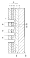
- FIG. 3 is a schematic cross-sectional view illustrating a configuration example of a semiconductor laser according to an embodiment of the present disclosure.
- FIG. 2 is a plan view showing one configuration example of the semiconductor laser shown in FIG. 1 as seen from the semiconductor laminated body side.
- FIG. 2 is a plan view showing one configuration example of the semiconductor laser shown in FIG. 1 viewed from the substrate side.
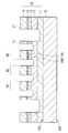
- It is a schematic cross section which shows one structural example of the light-emitting device which mounted the semiconductor laser shown in FIG. 1 on the mounting substrate.
- FIG. 6 is a schematic cross sectional view illustrating the method for manufacturing the semiconductor laser shown in FIG. 1. It is a cross-sectional schematic diagram showing 1 process following FIG. 5A. It is a cross-sectional schematic diagram showing 1 process following FIG. 5B.
- FIG. 5C It is a cross-sectional schematic diagram showing 1 process following FIG. 5C. It is a cross-sectional schematic diagram showing 1 process following FIG. 5D. It is a cross-sectional schematic diagram showing 1 process following FIG. 5E. It is a cross-sectional schematic diagram showing 1 process following FIG. 5F. It is a cross-sectional schematic diagram showing 1 process following FIG. 5G.
- FIG. 1 illustrates a configuration example of a light emitting device (semiconductor laser 1) according to an embodiment of the present disclosure.
- the semiconductor laser 1 is a laser array in which a plurality of VCSELs are integrated.
- the semiconductor laser 1 has a semiconductor stacked body ST on the first surface 10A of the substrate 10.
- the substrate 10 is a specific example of the “substrate” of the present disclosure.
- the semiconductor stacked body ST is a specific example of the “semiconductor stacked body” of the present disclosure.
- the buffer layer 11, the first light reflection layer 12, the active layer 13, the current confinement layer 16, and the second light reflection layer 14 are stacked in this order on the first surface 10A of the substrate 10. It was done.
- the first concave portion 15 is provided in the first concave portion forming region R15 by etching, for example, from the second light reflecting layer 14 to a part of the first light reflecting layer 12. ing.
- the semiconductor stacked body ST is left without being etched, so that a plurality of (three in the drawing) mesa regions M1, M2, M3 are provided. There is.
- the mesa regions M1, M2, M3 have a columnar shape such as a columnar shape.
- the current confinement layer 16 forms a current confinement region 16B with a predetermined width from the outer periphery of the columnar shape.
- the portion inside the current confinement region 16B when viewed from the outer peripheral side of the columnar shape is the current injection region 16A.
- the current injection region 16A of each of the mesa regions M1, M2, M3 corresponds to light emitting regions L1, L2, L3 of the laser beams LT1, LT2, LT3 (described later).
- two second recesses 17 are formed on both sides of the first recess formation region R15 by etching, for example, from the second light reflection layer 14 to a part of the buffer layer 11. ing.
- a through opening 18A is formed in the buffer layer 11 and the substrate 10 in a partial region of the bottom surface of each second recess 17.
- the insulating film 22 is formed except for the surface of the semiconductor stacked body ST in each mesa region M1, M2, M3, the bottom surface of the second recess 17, and the inner wall surface of the through opening 18A. Has been formed.
- the through wiring 19 is formed inside the through opening 18A.
- a bottom conductive layer 20 is formed on the bottom surface of the second recess 17 so as to be connected to the through wiring 19.
- the through wiring 19 is a specific example of “through wiring” of the present disclosure.
- the electrode pad 23 is formed from the bottom surface of the second recess 17 to the side wall surface of the second recess 17 and the surface of the semiconductor stacked body ST so as to be connected to the bottom conductive layer 20.
- the electrode pad 23 is a specific example of the “first conductive layer” of the present disclosure.
- An n electrode 24 is formed on the second surface 10B of the substrate 10.
- the n-electrode 24 is a specific example of the “second conductive layer” of the present disclosure.
- the n-electrode 24 is provided so that a predetermined voltage can be applied to the semiconductor stacked body ST in each of the light emitting regions L1, L2, L3.
- the n-electrode 24 is provided with openings 24A corresponding to the light emitting areas L1, L2, L3, respectively, and opens the laser beams LT1, LT2, LT3 (described later) emitted in the light emitting areas L1, L2, L3. It can be led to the outside from the portion 24A.
- a p-electrode 21 is formed on the surface of the semiconductor stacked body ST in each of the mesa regions M1, M2, M3.
- FIG. 2 shows a plan configuration of the semiconductor laser 1 shown in FIG. 1 viewed from the semiconductor laminated body ST side.
- a cross-sectional structure taken along line XX 'shown in FIG. 2 is shown in FIG.
- the display of the insulating film 22 is omitted.
- the semiconductor stacked body ST is provided with the first recess 15 so that a plurality of (six in the drawing) mesa regions M1, M2, M3, M4, M5 and M6 are left in the first recess formation region R15.
- FIG. 1 shows a cross section that crosses three mesa regions M1, M2, M3 of the six mesa regions M1, M2, M3, M4, M5, M6. As shown in FIG.
- the p-electrode 21 is formed on the surface of the semiconductor stacked body ST in each of the mesa regions M1, M2, M3, M4, M5 and M6.
- a plurality of (two in the drawing) second recesses 17 are formed on both sides of the first recess formation region R15, and the second recesses 17 are formed in a part of the bottom surface of the second recess 17.
- a through opening 18A is formed.
- the through wiring 19 is formed inside the through opening 18A.
- the electrode pad 23 is formed from the bottom surface of the second recess 17 to the side wall surface of the second recess 17 and to the surface of the semiconductor stacked body ST.
- FIG. 3 shows a plane configuration of the semiconductor laser 1 shown in FIG. 1 viewed from the substrate 10 side.
- a cross-sectional structure taken along line XX 'shown in FIG. 3 is shown in FIG.
- the n-electrode 24 is formed on the second surface 10B of the substrate 10.
- the n-electrode 24 is provided with openings 24A corresponding to the respective light emitting regions L1, L2, L3, L4, L5 and L6.
- the six light emitting regions L1, L2, L3, L4, L5 and L6 are VCSELs. That is, the semiconductor laser 1 is a laser array in which six VCSELs are integrated.
- FIG. 1 to FIG. 3 show a configuration in which six VCSELs are integrated, the number of integrated VCSELs is not limited, and for example, a configuration in which several tens to several thousands are integrated may be used.
- the substrate 10 is composed of, for example, a gallium arsenide (GaAs) substrate.
- the substrate 10 may be made of indium phosphide (InP), gallium nitride (GaN), silicon (Si), silicon carbide (SiC), or the like depending on the material system of the light emitting device, the bonding process of different substrates, and the like.
- the buffer layer 11 is made of, for example, GaAs.
- the buffer layer 11 is provided as a contact layer that electrically connects the substrate 10 and the first light reflection layer 12.
- the first light reflection layer 12 is a DBR (Distributed Bragg Reflector) layer arranged between the buffer layer 11 and the active layer 13.
- the first light reflection layer 12 faces the second light reflection layer 14 with the active layer 13 and the current constriction layer 16 in between.
- the first light reflection layer 12 resonates the light generated in the active layer 13 with the second light reflection layer 14.
- the first light reflecting layer 12 has a laminated structure in which low refractive index layers and high refractive index layers are alternately stacked.
- the low refractive index layer is, for example, n-type Al X1 Ga (1-X1) As (0 ⁇ X1 ⁇ 1) having an optical film thickness of ⁇ / 4.
- ⁇ represents the oscillation wavelength of the laser light emitted from each of the light emitting regions L1, L2, L3, L4, L5, L6.
- the high refractive index layer is, for example, n-type Al X2 Ga (1-X2) As (0 ⁇ X2 ⁇ 1) having an optical film thickness of ⁇ / 4.
- the active layer 13 is provided between the first light reflecting layer 12 and the second light reflecting layer 14.
- the active layer 13 is made of, for example, an aluminum gallium arsenide (AlGaAs) -based semiconductor material.
- AlGaAs aluminum gallium arsenide
- the active layer 13 receives the holes injected from the p electrode 21 through the current injection region 16A to generate stimulated emission light.
- AlGaAs aluminum gallium arsenide
- the active layer 13 receives the holes injected from the p electrode 21 through the current injection region 16A to generate stimulated emission light.
- undoped Al X3 Ga (1-X3) As (0 ⁇ X3 ⁇ 1) can be used.
- the active layer 13 may have a multi quantum well (MQW) structure of GaAs and AlGaAs, for example.
- the active layer 13 may be configured by a multiple quantum well structure of indium gallium arsenide (InGaAs) and AlGaAs.
- the current confinement region 16B is formed in the current confinement layer 16 in an annular shape having a predetermined width from the outer peripheral side of the columnar shape of each mesa region M1, M2, M3, M4, M5, M6 to the inside.
- the portion inside the current confinement region 16B when viewed from the outer peripheral side of the columnar shape is the current injection region 16A.
- the current confinement region 16B can be formed, for example, by subjecting the current confinement layer 16 to oxidation treatment from the outer peripheral side of the columnar shape of each mesa region M1, M2, M3, M4, M5, M6.
- the current confinement layer 16 is formed of, for example, p-type Al X4 Ga (1-X4) As (0.9 ⁇ X4 ⁇ 1).
- the current confinement region 16B is formed by oxidizing the current confinement layer 16 and contains, for example, aluminum oxide (AlO x ).
- the current injection region 16A is a portion that is not oxidized inside the current confinement region 16B.
- the radius of the substantially circular current injection region 16A is, for example, 1 ⁇ m to 20 ⁇ m.
- the second light reflection layer 14 is a DBR layer arranged between the current confinement layer 16 and the insulating film 22.
- the second light reflection layer 14 faces the first light reflection layer 12 with the current confinement layer 16 and the active layer 13 interposed therebetween.
- the second light reflection layer 14 has a laminated structure in which low refractive index layers and high refractive index layers are alternately stacked.
- the low refractive index layer is, for example, n-type Al X5 Ga (1-X5) As (0 ⁇ X5 ⁇ 1) having an optical film thickness of ⁇ / 4.
- the high refractive index layer is, for example, n-type Al X6 Ga (1-X6) As (0 ⁇ X6 ⁇ 1) having an optical film thickness of ⁇ / 4.
- the insulating film 22 is made of an insulating material such as silicon nitride (SiN) or silicon oxide (SiO 2 ).
- the through wiring 19 is formed of a metal such as gold (Au), copper (Cu), nickel (Ni), or the like.
- the bottom conductive layer 20 is formed of a multi-layer film of a metal such as gold germanium (AuGe) / nickel / gold.
- the electrode pad 23 is formed of a multilayer film of metal such as titanium (Ti) / gold.
- the p-electrode 21 is, for example, gold, germanium (Ge), silver (Ag), palladium (Pd), platinum (Pt), nickel, titanium, vanadium (V), tungsten (W), chromium (Cr), aluminum ( It is formed of a single layer film or a multilayer film of a metal such as Al), copper, zinc (Zn), tin (Sn), and indium (In). For example, a titanium / platinum / gold multilayer film is used.
- the n-electrode 24 is formed of, for example, a single-layer film or a multi-layer film of the same metal as the p-electrode 21.
- the n-electrode 24 may be formed of a transparent electrode such as ITO (Indium-Tin-Oxide, tin-doped indium oxide), zinc oxide, tin oxide, and titanium oxide.
- ITO Indium-Tin-Oxide, tin-doped indium oxide
- the n-electrode 24 can have a material configuration and a pattern formed in consideration of thermal conductivity, and can enhance the heat dissipation of the substrate 10.
- FIG. 4 shows a configuration example of a light emitting device in which the semiconductor laser shown in FIG. 1 is mounted on a mounting board.
- the light emitting device 3 is configured by flip-chip mounting the semiconductor laser 1 shown in FIG. 1 on a mounting substrate 2.
- the flip-chip mounting is mounting in such a manner that the surface of the semiconductor laser 1 on which the electrode pad 23 and the p electrode 21 are formed faces the mounting substrate 2.
- the mounting substrate 2 has, for example, a first electrode 51 and a second electrode 52 on a substrate 50.
- the first electrode 51 is provided on the p-electrode 21 of the semiconductor laser 1 and the second electrode 52 is provided on the electrode pad 23 of the semiconductor laser 1 in a corresponding pattern.
- the connection between the first electrode 51 and the p-electrode 21 and the connection between the second electrode 52 and the electrode pad 23 should be made by, for example, soldering or using an anisotropic conductive adhesive or an anisotropic conductive sheet.
- the mounting substrate 2 may be provided with a drive circuit such as a power supply circuit for the semiconductor laser 1. In that case, the terminal itself of the drive circuit may be connected to the p electrode 21 and the electrode pad 23 of the semiconductor laser 1.
- the electrode pad 23 is connected to the n electrode 24 via the bottom conductive layer 20 and the through wiring 19, so that the p electrode 21 and A voltage is applied from the n-electrode 24 to the semiconductor stacked body ST in each of the mesa regions M1, M2 and M3.
- electrons are injected from the n-electrode 24 and holes are injected from the p-electrode 21 in each of the light emitting regions L1, L2 and L3.
- the light generated by the recombination of electrons and holes is resonated and amplified between the pair of DBR layers (the first light reflection layer 12 and the second light reflection layer 14), passes through the opening 24A, and is transmitted to the substrate.
- Laser lights LT1, LT2 and LT3 are emitted from the 10 side. Although omitted in FIG. 4, the same applies to the mesa regions M4, M5, and M6.
- each light emitting region L1, L2, L3 may vary.
- the voltage applied to L3 may vary.
- the n-electrode 24 is provided so that a predetermined voltage can be applied to each of the light emitting regions L1, L2 and L3.
- the voltage application from the n-electrode 24 to the light emitting regions L1, L2, L3 can be performed uniformly regardless of the positions of the light emitting regions L1, L2, L3.
- the p electrode 21 is individually provided in each of the light emitting regions L1, L2, L3, and individually connected to the first electrode 51 of the mounting substrate 2. Accordingly, the voltage application from the p-electrode 21 to the light emitting regions L1, L2, L3 can be performed by selecting each of the light emitting regions L1, L2, L3. That is, it can be driven so that the laser beams LT1, LT2, LT3 are individually emitted from the selected light emitting regions L1, L2, L3 among the plurality of light emitting regions L1, L2, L3.
- the laser light LT1, LT2, LT3 has been described as being emitted through the opening 24A, but the present technology is not limited to this.
- the n-electrode 24 is formed of a transparent electrode such as ITO and is transparent to the laser light LT1, LT2, LT3, the laser light LT1, LT2, LT3 is not shielded by the n-electrode 24, so the opening 24A is It need not be provided.
- the emission directions of the laser beams LT1, LT2, LT3 may not be toward the substrate 10 side.
- members having a light shielding property such as wiring and electrodes are arranged at positions that do not interfere with the emission of the laser beams LT1, LT2, LT3. ..
- the number of electrode pads 23 is smaller than the number of p electrodes 21. Since the p-electrodes 21 are provided in the respective light emitting areas L1, L2, L3 as described above, the number of the p-electrodes 21 corresponds to the number of the light emitting areas L1, L2, L3.
- the electrode pad 23 is provided so as to be connected to the n-electrode 24 that is a common electrode for the plurality of light emitting regions L1, L2, L3, and the semiconductor laser 1 is provided with two electrode pads 23. It suffices that at least one electrode pad 23 is provided, and the number can be smaller than the number of p electrodes 21. It is preferable that the number of the electrode pads 23 is smaller because the structure of the semiconductor laser 1 becomes simpler and the manufacturing becomes easier.
- a buffer layer 11, a first light reflection layer 12, an active layer 13, a current confinement layer 16, and a second light reflection layer 14 are laminated in this order on a substrate 10, and a semiconductor is formed.
- the stacked body ST is formed.
- the semiconductor laminated body ST is formed by epitaxial crystal growth using a method such as a molecular beam epitaxy (MBE) method or a metal organic chemical vapor deposition (MOCVD) method.
- MBE molecular beam epitaxy
- MOCVD metal organic chemical vapor deposition
- a resist film (not shown) having a predetermined pattern is formed by patterning on the upper layer of the semiconductor stacked body ST by a photolithography process, and the second light reflection layer 14 to the first light is formed.
- a part of the reflective layer 12 is removed by etching to form the first recess 15.
- the etching is performed by, for example, reactive ion etching (RIE).
- RIE reactive ion etching
- the resist film is formed so as to have a pattern for protecting the mesa regions M1, M2, M3.
- the pillar-shaped semiconductor stacked body ST is left in the mesa regions M1, M2, M3 by the above etching process.
- the resist film is removed.
- the current confinement layer 16 is oxidized with a predetermined width from the outer periphery of the columnar shape in the mesa regions M1, M2, M3 to form the current confinement region 16B.
- the region inside the current confinement region 16B is the current injection region 16A.
- a resist film (not shown) having a predetermined pattern is patterned on the upper layer of the semiconductor stacked body ST, and the second light reflection layer 14 to a part of the buffer layer 11 are formed.
- the second recess 17 is formed by removing it by etching such as RIE.
- the resist film is removed.
- a resist film (not shown) having a predetermined pattern is patterned on the upper layer of the semiconductor stacked body ST, and a part of the substrate 10 is formed on a part of the bottom of the second recess 17. Are removed by etching such as RIE to form a through wiring recess 18. Next, the resist film is removed.
- an insulating film 22 such as silicon nitride is formed by, for example, a chemical vapor deposition (CVD) method or an atomic layer deposition (ALD) method.
- the insulating film 22 is formed so as to cover the inner wall surface of the first recess 15 and the inner wall surface of the second recess 17.
- a resist film (not shown) having a predetermined pattern is formed on the upper layer of the semiconductor stacked body ST, and etching such as RIE is performed, so that each of the mesa regions M1, M2, and M2 on the surface of the semiconductor stacked body ST is formed.
- the insulating film 22 on the surface of the semiconductor stacked body ST in M3, the bottom surface of the second recess 17 and the inner wall surface of the through wiring recess 18 is removed.
- gold or the like is embedded in the recess 18 for the through wiring to form the through wiring 19.
- a bottom conductive layer 20 is formed by depositing a metal multilayer film of AuGe / Ni / Au on the bottom of the second recess 17 by, for example, a metal vapor deposition method.
- a p-electrode 21 is formed by forming a Ti / Pt / Au metal multilayer film on the surface of the semiconductor stacked body ST in each of the mesa regions M1, M2, and M3 by, for example, a sputtering method.
- a multilayer film of Ti / Au metal is formed from the bottom surface of the second recess 17 to the side wall surface of the second recess 17 and the surface of the semiconductor stacked body ST by, for example, a sputtering method.
- the electrode pad 23 is formed so as to be connected to the bottom surface conductive layer 20.
- the second surface 10B of the substrate 10 is polished by, for example, a chemical mechanical polishing (CMP) process until the through wiring 19 is exposed.
- CMP chemical mechanical polishing
- the n-electrode 24 is formed by forming a metal multilayer film of AuGe / Ni / Au on the second surface 10B of the substrate 10 by, for example, a metal vapor deposition method.
- the n-electrode 24 is provided with openings 24A corresponding to the light emitting regions L1, L2, L3 in the respective mesa regions M1, M2, M3, and the semiconductor laser 1 is completed.
- the operation of the semiconductor laser 1 of this embodiment will be described with reference to FIG.
- the semiconductor laser 1 when a predetermined voltage is applied to the p electrode 21 and the electrode pad 23, the voltage is applied from the p electrode 21 and the n electrode 24 to the semiconductor stacked body ST in each of the mesa regions M1, M2, M3.
- the semiconductor stacked body ST in each of the mesa regions M1, M2, M3.
- electrons are injected from the n electrode 24 and holes are injected from the p electrode 21, and light is generated by recombination of the electrons and holes.
- the light resonates and is amplified between the pair of DBR layers, and the laser light LT1, LT2, LT3 is emitted from the substrate 10 side through the opening 24A.
- the n electrode 24 is provided on the second surface of the substrate 10 so that a predetermined voltage can be applied to each of the light emitting regions L1, L2, L3.
- the n-electrode 24 is connected to the electrode pad 23 via the through wiring 19, and a voltage can be applied to the n-electrode 24 from the electrode pad 23 provided on the second surface 10B of the substrate 10.
- the n electrode 24 is provided on the second surface of the substrate 10 so that a predetermined voltage can be applied to each of the light emitting regions L1, L2, L3.
- a voltage to the n-electrode 24 it is possible to uniformly apply a voltage to the light emitting regions L1, L2, L3 regardless of the positions of the light emitting regions L1, L2, L3.
- the semiconductor laser 1 is provided with the p-electrode 21 and the electrode pad 23 on the same surface (second surface 10B) of the substrate 10, flip-chip mounting is possible.
- the laser since the p-electrode 21 is individually provided in each of the light emitting areas L1, L2, L3, the laser is individually emitted from the selected light emitting areas L1, L2, L3 of the light emitting areas L1, L2, L3. It can be driven so as to emit the light LT1, LT2, LT3.
- the n-electrode 24 can have a material configuration and pattern formation in consideration of thermal conductivity, and can enhance the heat dissipation of the substrate 10.
- the semiconductor laser having six VCSELs has been described, but the present invention is not limited to this, and instead of this, it can be applied to a semiconductor laser having several tens to several thousands integrated. As the number of integrated lasers increases, the distance between the light emitting region of each laser and the n-electrode may vary, but according to the present technology, the voltage difference is applied to the light emitting region of each laser with a small voltage difference. can do.
- This technology can be applied to various electronic devices including semiconductor lasers.
- it can be applied to a light source provided in a mobile electronic device such as a smartphone, a light source of various sensing devices that detect a shape, a motion, and the like.
- the present technology can be configured as below. According to the present technology having the following configuration, a uniform voltage can be applied to the semiconductor stacked body in the plurality of light emitting regions, so that uniform light emitting characteristics can be obtained between the plurality of light emitting regions.
- a substrate having a first surface and a second surface facing each other, A semiconductor laminate provided on the first surface of the substrate and having a plurality of light emitting regions capable of emitting laser light; A first conductive layer provided on the surface of the semiconductor laminate opposite to the substrate; A second conductive layer that is provided on the second surface of the substrate and that is capable of applying a predetermined voltage to the semiconductor stacked body in each of the plurality of light emitting regions; A light-emitting device comprising: a through wiring that electrically connects the first conductive layer and the second conductive layer.
- the semiconductor laminated body includes a first light-reflecting layer, an active layer, and a second light-reflecting layer sequentially laminated from the substrate side.
- the semiconductor stacked body further includes a current confinement layer having a current injection region between the active layer and the second light reflection layer.
- the semiconductor stacked body has a plurality of mesa regions each including a plurality of the light emitting regions.
- a light emitting device flip-chip mounted on a mounting substrate The light emitting device is A substrate having a first surface and a second surface facing each other; A semiconductor laminate provided on the first surface of the substrate and having a plurality of light emitting regions capable of emitting laser light; A first conductive layer provided on the surface of the semiconductor laminate opposite to the substrate; A second conductive layer that is provided on the second surface of the substrate and that is capable of applying a predetermined voltage to the semiconductor stacked body in each of the plurality of light emitting regions; A light-emitting device comprising: a through wiring that electrically connects the first conductive layer and the second conductive layer.
Landscapes
- Physics & Mathematics (AREA)
- Condensed Matter Physics & Semiconductors (AREA)
- General Physics & Mathematics (AREA)
- Electromagnetism (AREA)
- Optics & Photonics (AREA)
- Semiconductor Lasers (AREA)
Abstract
本開示の一実施の形態の発光デバイスは、対向する第1の面及び第2の面を有する基板と、基板の前記第1の面に設けられるとともにレーザ光を出射可能な複数の発光領域を有する半導体積層体と、基板とは反対側の半導体積層体の表面に設けられた第1の導電層と、基板の第2の面に設けられるとともに複数の発光領域のそれぞれにおいて半導体積層体に所定の電圧を印加可能に設けられた第2の導電層と、第1の導電層と第2の導電層とを電気的に接続する貫通配線とを備える。
Description
本開示は、発光デバイス及び発光装置に関する。
複数の発光領域を有する面発光半導体レーザの開発が進められている(例えば、特許文献1及び特許文献2参照)。面発光半導体レーザは、例えばVCSEL(Vertical Cavity Surface Emitting LASER)である。
ところで、複数の発光領域を有する発光デバイスでは、複数の発光領域が均一な発光特性を有することが望まれる。
複数の発光領域間で均一な発光特性を得ることが可能な発光デバイス及び発光デバイスを用いた発光装置を提供することが望ましい。
本開示の一実施の形態における発光デバイスは、基板と、半導体積層体と、第1の導電層と、第2の導電層と、貫通配線とを備えたものである。基板は、対向する第1の面及び第2の面を有する。半導体積層体は、基板の第1の面に設けられるとともにレーザ光を出射可能な複数の発光領域を有する。第1の導電層は、基板とは反対側の半導体積層体の表面に設けられている。第2の導電層は、基板の第2の面に設けられるとともに複数の発光領域のそれぞれにおいて半導体積層体に所定の電圧を印加可能に設けられている。貫通配線は、第1の導電層と第2の導電層とを電気的に接続するように設けられている。
本開示の一実施の形態における発光装置は、実装基板にフリップチップ実装された発光デバイスを備えたものであり、発光デバイスとして、上記本開示の一実施の形態の発光デバイスを有する。
本開示の一実施の形態における発光デバイス及び一実施の形態における発光装置では、基板の第2の面に第2の導電層が設けられており、第2の導電層は貫通配線を介して第1の導電層に接続されている。第2の導電層から、複数の発光領域のそれぞれにおいて半導体積層体に所定の電圧を印加する。
以下、本開示の実施の形態について、図面を参照して詳細に説明する。なお、説明は以下の順序で行う。
1.実施の形態(基板の裏面に第2の導電層が設けられた例)
[構成例]
[半導体レーザの製造方法]
[動作]
[作用]
[効果]
1.実施の形態(基板の裏面に第2の導電層が設けられた例)
[構成例]
[半導体レーザの製造方法]
[動作]
[作用]
[効果]
<1.実施の形態>
[構成例]
図1は、本開示の一実施の形態に係る発光デバイス(半導体レーザ1)の一構成例を表すものである。半導体レーザ1は、複数のVCSELを集積したレーザアレイである。半導体レーザ1は、基板10の第1の面10A上に、半導体積層体STを有している。基板10は、本開示の「基板」の一具体例である。半導体積層体STは、本開示の「半導体積層体」の一具体例である。半導体積層体STは、基板10の第1の面10A上に、バッファ層11、第1の光反射層12、活性層13、電流狭窄層16、及び第2の光反射層14がこの順に積層されたものである。半導体積層体STには、第1の凹部形成領域R15において、例えば、第2の光反射層14から第1の光反射層12の一部までをエッチングすることで第1の凹部15が設けられている。第1の凹部15の形成領域のうちの一部の領域において、半導体積層体STがエッチングされずに残されることにより、複数(図面上3つ)のメサ領域M1,M2,M3が設けられている。メサ領域M1,M2,M3は、例えば円柱状等の柱状の形状を有している。メサ領域M1,M2,M3には、電流狭窄層16によって、柱状の形状の外周から所定の幅で電流狭窄領域16Bが形成されている。柱状の形状の外周側からみて電流狭窄領域16Bの内側の部分は、電流注入領域16Aである。各メサ領域M1,M2,M3の電流注入領域16Aは、レーザ光LT1,LT2,LT3(後述)の発光領域L1,L2,L3に対応する。
[構成例]
図1は、本開示の一実施の形態に係る発光デバイス(半導体レーザ1)の一構成例を表すものである。半導体レーザ1は、複数のVCSELを集積したレーザアレイである。半導体レーザ1は、基板10の第1の面10A上に、半導体積層体STを有している。基板10は、本開示の「基板」の一具体例である。半導体積層体STは、本開示の「半導体積層体」の一具体例である。半導体積層体STは、基板10の第1の面10A上に、バッファ層11、第1の光反射層12、活性層13、電流狭窄層16、及び第2の光反射層14がこの順に積層されたものである。半導体積層体STには、第1の凹部形成領域R15において、例えば、第2の光反射層14から第1の光反射層12の一部までをエッチングすることで第1の凹部15が設けられている。第1の凹部15の形成領域のうちの一部の領域において、半導体積層体STがエッチングされずに残されることにより、複数(図面上3つ)のメサ領域M1,M2,M3が設けられている。メサ領域M1,M2,M3は、例えば円柱状等の柱状の形状を有している。メサ領域M1,M2,M3には、電流狭窄層16によって、柱状の形状の外周から所定の幅で電流狭窄領域16Bが形成されている。柱状の形状の外周側からみて電流狭窄領域16Bの内側の部分は、電流注入領域16Aである。各メサ領域M1,M2,M3の電流注入領域16Aは、レーザ光LT1,LT2,LT3(後述)の発光領域L1,L2,L3に対応する。
半導体積層体STには、第1の凹部形成領域R15の両側において、例えば、第2の光反射層14からバッファ層11の一部までをエッチングすることで2つの第2の凹部17が形成されている。各第2の凹部17の底面の一部の領域には、バッファ層11及び基板10に貫通開口部18Aが形成されている。半導体積層体STの表面のうちの、各メサ領域M1,M2,M3における半導体積層体STの表面、第2の凹部17の底面、及び貫通開口部18Aの内壁面を除いて、絶縁膜22が形成されている。貫通開口部18Aの内側に貫通配線19が形成されている。第2の凹部17の底面に底面導電層20が貫通配線19に接続するように形成されている。貫通配線19は、本開示の「貫通配線」の一具体例である。第2の凹部17の底面から第2の凹部17の側壁面及び半導体積層体STの表面にかけて電極パッド23が底面導電層20に接続するように形成されている。電極パッド23は、本開示の「第1の導電層」の一具体例である。基板10の第2の面10Bには、n電極24が形成されている。n電極24は、本開示の「第2の導電層」の一具体例である。n電極24は、発光領域L1,L2,L3のそれぞれにおいて半導体積層体STに所定の電圧を印加可能に設けられている。n電極24には、発光領域L1,L2,L3に対応して開口部24Aがそれぞれ設けられており、発光領域L1,L2,L3で発せられたレーザ光LT1,LT2,LT3(後述)を開口部24Aから外部に導くことができる。各メサ領域M1,M2,M3における半導体積層体STの表面に、p電極21が形成されている。
図2は、図1に示した半導体レーザ1の半導体積層体ST側から見た平面構成を表すものである。図2に示したX-X’線に沿った断面構成が図1に表されている。図2においては、絶縁膜22の表示は省略している。半導体積層体STには、第1の凹部形成領域R15において、複数(図面上6つ)のメサ領域M1,M2,M3,M4,M5,M6を残すようにして、第1の凹部15が設けられている。図1では、6つのメサ領域M1,M2,M3,M4,M5,M6のうちの3つのメサ領域M1,M2,M3を横切る断面が表されている。図2に示したように、各メサ領域M1,M2,M3,M4,M5,M6において半導体積層体STの表面にp電極21が形成されている。半導体積層体STには、第1の凹部形成領域R15の両側において、複数(図面上2つ)の第2の凹部17が形成されており、第2の凹部17の底面の一部の領域に貫通開口部18Aが形成されている。貫通開口部18Aの内側に貫通配線19が形成されている。第2の凹部17の底面から第2の凹部17の側壁面の及び半導体積層体STの表面にかけて電極パッド23が形成されている。
図3は、図1に示した半導体レーザ1の基板10側から見た平面構成を表すものである。図3に示したX-X’線に沿った断面構成が図1に表されている。基板10の第2の面10Bに、n電極24が形成されている。n電極24には、各発光領域L1,L2,L3,L4,L5,L6に対応してそれぞれ開口部24Aが設けられている。
図1~図3に示した半導体レーザ1において、6つの発光領域L1,L2,L3,L4,L5,L6はそれぞれVCSELである。即ち、半導体レーザ1は6つのVCSELが集積したレーザアレイである。図1~図3では6つのVCSELを集積した構成を示しているが、集積する数に制限はなく、例えば数10~数1000個集積した構成とすることもできる。
基板10は、例えばガリウムヒ素(GaAs)基板により構成されている。基板10は、発光デバイスの材料系や異種基板の接合プロセス等により、インジウムリン(InP)、窒化ガリウム(GaN)、シリコン(Si)、または炭化シリコン(SiC)等により構成される場合もある。
バッファ層11は、例えばGaAs等から構成されている。バッファ層11は、基板10と第1の光反射層12とを電気的に接続するコンタクト層として設けられている。
第1の光反射層12は、バッファ層11と活性層13との間に配置されたDBR(Distributed Bragg Reflector)層である。第1の光反射層12は、活性層13及び電流狭窄層16を間にして第2の光反射層14と対向している。第1の光反射層12は、活性層13で発生した光を第2の光反射層14との間で共振させるようになっている。
第1の光反射層12は、低屈折率層及び高屈折率層を交互に重ねた積層構造を有している。低屈折率層は、例えば光学膜厚がλ/4のn型のAlX1Ga(1-X1)As(0<X1<1)である。λは、各発光領域L1,L2,L3,L4,L5,L6から発せられるレーザ光の発振波長を表す。高屈折率層は、例えば光学膜厚がλ/4のn型のAlX2Ga(1-X2)As(0<X2<1)である。
活性層13は、第1の光反射層12及び第2の光反射層14の間に設けられている。活性層13は、例えばアルミニウムガリウムヒ素(AlGaAs)系の半導体材料により構成されている。この活性層13では、p電極21から電流注入領域16Aを介して注入された正孔(ホール)を受けて誘導放出光を発生するようになっている。活性層13には、例えばアンドープのAlX3Ga(1-X3)As(0<X3<1)を用いることができる。活性層13は、例えばGaAsとAlGaAsとの多重量子井戸(MQW:Multi Quantum Well)構造を有していてもよい。インジウムガリウムヒ素(InGaAs)とAlGaAsとの多重量子井戸構造により活性層13を構成するようにしてもよい。
電流狭窄領域16Bは、電流狭窄層16において、各メサ領域M1,M2,M3,M4,M5,M6の柱状の形状の外周側から内側に所定の幅を有して環状に形成されている。柱状の形状の外周側からみて電流狭窄領域16Bの内側の部分は、電流注入領域16Aである。電流狭窄領域16Bは、例えば各メサ領域M1,M2,M3,M4,M5,M6の柱状の形状の外周側から電流狭窄層16に酸化処理を行うことによって形成できる。電流狭窄層16は、例えばp型のAlX4Ga(1-X4)As(0.9<X4<1)により形成されている。電流狭窄領域16Bは電流狭窄層16が酸化されて形成され、例えば酸化アルミニウム(AlOX)を含んでいる。電流注入領域16Aは、電流狭窄領域16Bの内側に
おいて酸化されなかった部分である。電流狭窄構造を設けることにより、p電極21から活性層13に注入される電流の電流狭窄がなされ、電流注入効率が高められる。略円状の電流注入領域16Aの半径は、例えば、1μm~20μmである。
おいて酸化されなかった部分である。電流狭窄構造を設けることにより、p電極21から活性層13に注入される電流の電流狭窄がなされ、電流注入効率が高められる。略円状の電流注入領域16Aの半径は、例えば、1μm~20μmである。
第2の光反射層14は、電流狭窄層16と絶縁膜22との間に配置されたDBR層である。第2の光反射層14は、電流狭窄層16及び活性層13を間にして第1の光反射層12と対向している。
第2の光反射層14は、低屈折率層及び高屈折率層を交互に重ねた積層構造を有している。低屈折率層は、例えば光学膜厚がλ/4のn型のAlX5Ga(1-X5)As(0<X5<1)である。高屈折率層は、例えば光学膜厚がλ/4のn型のAlX6Ga(1-X6)As(0<X6<1)である。
絶縁膜22は、例えば窒化シリコン(SiN)あるいは酸化シリコン(SiO2)等の
絶縁体で形成されている。
絶縁体で形成されている。
貫通配線19は、例えば金(Au)、銅(Cu)、ニッケル(Ni)等の金属により形成されている。底面導電層20は、例えば金ゲルマニウム(AuGe)/ニッケル/金等の金属の多層膜で形成されている。電極パッド23は、例えばチタン(Ti)/金等の金属の多層膜で形成されている。
p電極21は、例えば、金、ゲルマニウム(Ge)、銀(Ag)、パラジウム(Pd)、白金(Pt)、ニッケル、チタン、バナジウム(V)、タングステン(W)、クロム(Cr)、アルミニウム(Al)、銅、亜鉛(Zn)、スズ(Sn)、及びインジウム(In)等の金属の単層膜あるいは多層膜により形成されている。例えば、チタン/白金/金の多層膜が用いられる。
n電極24は、例えばp電極21と同様の金属の単層膜あるいは多層膜により形成されている。あるいは、n電極24は、ITO(Indium-Tin-Oxide、スズドープ酸化インジウム)、酸化亜鉛、酸化スズ、及び酸化チタン等の透明電極により形成されていてもよい。n電極24は、熱伝導性も考慮して材料構成やパターン形成をすることが可能であり、基板10の放熱性を高めることができる。
図4は、図1に示した半導体レーザを実装基板に実装した発光装置の一構成例を表すものである。発光装置3は、図1に示した半導体レーザ1が実装基板2にフリップチップ実装されて構成されている。フリップチップ実装とは、半導体レーザ1の電極パッド23及びp電極21の形成面が実装基板2に面するように実装されるものである。実装基板2は、例えば基板50に第1電極51及び第2電極52を有する。第1電極51は半導体レーザ1のp電極21に、第2電極52は半導体レーザ1の電極パッド23に、それぞれ対応するパターンで設けられている。第1電極51とp電極21との接続、及び第2電極52と電極パッド23との接続は、例えばハンダによる接続や、異方性導電接着剤あるいは異方性導電シート等を用いて行うことができる。実装基板2には、半導体レーザ1への電源供給回路等の駆動回路が設けられていてもよい。その場合、駆動回路の端子そのものが、半導体レーザ1のp電極21及び電極パッド23に接続される構成であってもよい。
半導体レーザ1では、p電極21及び電極パッド23に所定の電圧を印加すると、電極パッド23は、底面導電層20及び貫通配線19を介してn電極24に接続しているので、p電極21及びn電極24から各メサ領域M1,M2,M3の半導体積層体STに電圧が印加される。これにより、各発光領域L1,L2,L3において、n電極24から電子が注入され、p電極21からホールが注入される。電子及びホールが再結合して発生した光が、1対のDBR層(第1の光反射層12及び第2の光反射層14)間で共振して増幅され、開口部24Aを通って基板10側からレーザ光LT1、LT2,LT3が出射される。図4では省略しているが、メサ領域M4,M5,M6においても同様である。
n電極24が設けられておらず、基板10を通して各発光領域L1,L2,L3に電圧を印加しようとすると、基板10の電気抵抗(基板10を電流が流れる際の電圧降下)のために、各発光領域L1,L2,L3に印加される電圧にばらつきが生じる場合がある。n電極24からの距離が異なる発光領域L1,L2,L3がある場合でも同様で、基板10の電気抵抗(基板10を電流が流れる際の電圧降下)のために、各発光領域L1,L2,L3に印加される電圧にばらつきが生じる場合がある。半導体レーザ1では、n電極24は発光領域L1,L2,L3のそれぞれにおいて所定の電圧を印加可能に設けられている。これにより、半導体レーザ1では、発光領域L1,L2,L3に対するn電極24からの電圧印加は、発光領域L1,L2,L3の位置によらずに均一に行うことができる。
発光装置3を構成する半導体レーザ1では、p電極21は各発光領域L1,L2,L3に個別に設けられ、個別に実装基板2の第1電極51に接続されている。これにより、p電極21から発光領域L1,L2,L3への電圧印加は、発光領域L1,L2,L3毎に選択して行うことこができる。即ち、複数の発光領域L1,L2,L3のうちの選択された発光領域L1,L2,L3から個別にレーザ光LT1,LT2,LT3を出射させるように駆動できる。
半導体レーザ1では、レーザ光LT1,LT2,LT3は開口部24Aを通って出射される構成について説明しているが、本技術はこれに限らない。例えばn電極24がITO等の透明電極で形成されていてレーザ光LT1,LT2,LT3に対して透過性を有する場合、n電極24によりレーザ光LT1,LT2,LT3は遮光されないので開口部24Aは設けなくてもよい。また、レーザ光LT1,LT2,LT3の出射方向は、基板10側でなくてもよい。半導体積層体STの側からレーザ光LT1,LT2,LT3が出射される場合には、配線及び電極等の遮光性を有する部材がレーザ光LT1,LT2,LT3の出射を妨げない位置に配置される。
半導体レーザ1では、電極パッド23の数は、p電極21の数より少ない構成である。p電極21は、上記のように各発光領域L1,L2,L3にそれぞれ設けられているのでp電極21の数は、発光領域L1,L2,L3の数に対応する。電極パッド23は、複数の発光領域L1,L2,L3に対する共通の電極であるn電極24に接続するように設けられたものであり、半導体レーザ1では2つの電極パッド23が設けられている。電極パッド23は少なくとも1つあればよく、p電極21の数より少ない数で構成することができる。電極パッド23の数は、少ないほど半導体レーザ1の構成が簡単となり、製造も容易となるので好ましい。
[半導体レーザの製造方法]
次に、図5A~図5Hを参照して、半導体レーザ1の製造方法について説明する。図5A~図5Hは、それぞれ、半導体レーザ1の製造方法における一工程を表すものである。
次に、図5A~図5Hを参照して、半導体レーザ1の製造方法について説明する。図5A~図5Hは、それぞれ、半導体レーザ1の製造方法における一工程を表すものである。
まず、図5Aに示したように、基板10に、バッファ層11、第1の光反射層12、活性層13、電流狭窄層16、及び第2の光反射層14をこの順に積層し、半導体積層体STを形成する。半導体積層体STの形成は、例えば分子線エピタキシー(MBE:Molecular Beam Epitaxy)法または有機金属化学気相成長(MOCVD:Metal Organic Chemical Vapor Deposition)法等の方法を用いたエピタキシャル結晶成長により行う。
次に、図5Bに示したように、半導体積層体STの上層に、フォトリソグラフィー工程により所定のパターンのレジスト膜(不図示)をパターン形成し、第2の光反射層14から第1の光反射層12の一部までをエッチング除去して第1の凹部15を形成する。エッチングは、例えば反応性イオンエッチング(RIE:Reactive Ion Etching)により行う。ここで、上記のレジスト膜は、メサ領域M1,M2,M3を保護するパターンとなるように形成する。これにより、上記のエッチング処理ではメサ領域M1,M2,M3において柱状の形状の半導体積層体STが残される。続いてレジスト膜を除去する。次に、水蒸気雰囲気中の高温処理を施すことで、メサ領域M1,M2,M3における柱状の形状の外周から所定の幅で電流狭窄層16を酸化し、電流狭窄領域16Bを形成する。電流狭窄領域16Bの内側の領域が電流注入領域16Aである。
続いて、図5Cに示したように、半導体積層体STの上層に、所定のパターンのレジスト膜(不図示)をパターン形成し、第2の光反射層14からバッファ層11の一部までをRIE等のエッチングにより除去して第2の凹部17を形成する。次に、レジスト膜を除去する。
続いて、図5Dに示したように、半導体積層体STの上層に、所定のパターンのレジスト膜(不図示)をパターン形成し、第2の凹部17の底部の一部において基板10の一部までをRIE等のエッチングにより除去して貫通配線用凹部18を形成する。次に、レジスト膜を除去する。
続いて、図5Eに示したように、例えば化学気相成長(CVD:Chemical Vapor Deposition)法あるいは原子層堆積(ALD:Atomic Layer Deposition)法により窒化シリコン等の絶縁膜22を形成する。絶縁膜22は、第1の凹部15の内壁面及び第2の凹部17の内壁面を被覆するように形成する。次に、半導体積層体STの上層に、所定のパターンのレジスト膜(不図示)をパターン形成し、RIE等のエッチングを行い、半導体積層体STの表面のうちの、各メサ領域M1,M2,M3における半導体積層体STの表面、第2の凹部17の底面、及び貫通配線用凹部18の内壁面における絶縁膜22を除去する。次に、例えば電気メッキ処理等により、貫通配線用凹部18の内部に金等を埋め込み、貫通配線19を形成する。続いて、例えば金属蒸着法等により、第2の凹部17の底部においてAuGe/Ni/Auの金属の多層膜を成膜することで底面導電層20を形成する。次に、例えばスパッタリング法等により、各メサ領域M1,M2,M3における半導体積層体STの表面にTi/Pt/Auの金属の多層膜を成膜することでp電極21を形成する。
続いて、図5Fに示したように、例えばスパッタリング法等により、第2の凹部17の底面から第2の凹部17の側壁面及び半導体積層体STの表面にかけてTi/Auの金属の多層膜を形成することで、底面導電層20に接続するように電極パッド23を形成する。
次に、図5Gに示したように、例えば化学的機械研磨(CMP:Chemical Mechanical Polishing)処理により、貫通配線19が露出するまで、基板10の第2の面10Bを研
磨する。
磨する。
続いて、図5Hに示したように、例えば金属蒸着法等により、基板10の第2の面10BにAuGe/Ni/Auの金属の多層膜を成膜することでn電極24を形成する。n電極24には、各メサ領域M1,M2,M3における発光領域L1,L2,L3に対応する開口部24Aを設けて、半導体レーザ1を完成させる。
[動作]
続いて、本実施の形態の半導体レーザ1の動作について、図1を参照して説明する。半導体レーザ1では、p電極21及び電極パッド23に所定の電圧を印加すると、p電極21及びn電極24から各メサ領域M1,M2,M3の半導体積層体STに電圧が印加される。これにより、各発光領域L1,L2,L3において、n電極24から電子が注入され、p電極21からホールが注入され、電子及びホールの再結合により光が発生する。光は1対のDBR層間で共振して増幅され、開口部24Aを通って基板10側からレーザ光LT1、LT2,LT3が出射される。
続いて、本実施の形態の半導体レーザ1の動作について、図1を参照して説明する。半導体レーザ1では、p電極21及び電極パッド23に所定の電圧を印加すると、p電極21及びn電極24から各メサ領域M1,M2,M3の半導体積層体STに電圧が印加される。これにより、各発光領域L1,L2,L3において、n電極24から電子が注入され、p電極21からホールが注入され、電子及びホールの再結合により光が発生する。光は1対のDBR層間で共振して増幅され、開口部24Aを通って基板10側からレーザ光LT1、LT2,LT3が出射される。
[作用]
本実施の形態の半導体レーザ1では、基板10の第2の面にn電極24が発光領域L1,L2,L3のそれぞれにおいて所定の電圧を印加可能に設けられている。n電極24は貫通配線19を介して電極パッド23が接続されており、基板10の第2の面10Bに設けられた電極パッド23からn電極24に電圧を印加できる。
本実施の形態の半導体レーザ1では、基板10の第2の面にn電極24が発光領域L1,L2,L3のそれぞれにおいて所定の電圧を印加可能に設けられている。n電極24は貫通配線19を介して電極パッド23が接続されており、基板10の第2の面10Bに設けられた電極パッド23からn電極24に電圧を印加できる。
[効果]
以上のように本実施の形態の半導体レーザ1では、基板10の第2の面にn電極24が発光領域L1,L2,L3のそれぞれにおいて所定の電圧を印加可能に設けられている。n電極24に電圧を印加することで、発光領域L1,L2,L3の位置によらずに均一に、発光領域L1,L2,L3に対して電圧印加を行うことができる。
以上のように本実施の形態の半導体レーザ1では、基板10の第2の面にn電極24が発光領域L1,L2,L3のそれぞれにおいて所定の電圧を印加可能に設けられている。n電極24に電圧を印加することで、発光領域L1,L2,L3の位置によらずに均一に、発光領域L1,L2,L3に対して電圧印加を行うことができる。
半導体レーザ1は、基板10の同じ面(第2の面10B)にp電極21及び電極パッド23が設けられているので、フリップチップ実装が可能である。
半導体レーザ1では、p電極21が各発光領域L1,L2,L3に個別に設けられているので、発光領域L1,L2,L3のうちの選択された発光領域L1,L2,L3から個別にレーザ光LT1,LT2,LT3を出射させるように駆動できる。
半導体レーザ1では、n電極24は、熱伝導性も考慮して材料構成やパターン形成をすることが可能であり、基板10の放熱性を高めることができる。
以上のことから、発光領域L1,L2,L3の間のレーザ光の発光特性を均一化することができる。
以上、実施の形態により説明したが、本技術は上記実施の形態には限定されず、種々の変形が可能である。
上記実施の形態では、6つのVCSELを有する半導体レーザについて説明したが、これに限定されるものではなく、これに代えて、例えば数10~数1000個集積した半導体レーザにも適用できる。集積するレーザの数が多くなるほど各レーザの発光領域とn電極との間の距離にばらつきが生じる場合があるが、本技術によれば各レーザの発光領域に電圧差を小さく抑えて電圧を印加することができる。
本技術は半導体レーザを含む種々の電子機器に適用できる。例えば、スマートフォン等の携帯電子機器に備えられる光源や、形状や動作等を検知する各種センシング機器の光源等に適用できる。
なお、本明細書に記載された効果はあくまで例示であって限定されるものではなく、また他の効果があってよい。
なお、本技術は以下のような構成とすることができる。以下の構成の本技術によれば、複数の発光領域の半導体積層体に対して均一な電圧が印加できるようになるため、複数の発光領域間で均一な発光特性を得ることが可能となる。
(1)対向する第1の面及び第2の面を有する基板と、
前記基板の前記第1の面に設けられるとともにレーザ光を出射可能な複数の発光領域を有する半導体積層体と、
前記基板とは反対側の前記半導体積層体の表面に設けられた第1の導電層と、
前記基板の前記第2の面に設けられるとともに複数の前記発光領域のそれぞれにおいて前記半導体積層体に所定の電圧を印加可能に設けられた第2の導電層と、
前記第1の導電層と前記第2の導電層とを電気的に接続する貫通配線と
を備える発光デバイス。
(2)前記半導体積層体は、第1の光反射層と、活性層と、第2の光反射層とが、前記基板側から順に積層されている
前記(1)に記載の発光デバイス。
(3)前記半導体積層体は、前記活性層と前記第2の光反射層との間に、電流注入領域を有する電流狭窄層をさらに有する
前記(2)に記載の発光デバイス。
(4)前記半導体積層体は、複数の前記発光領域をそれぞれ含む複数のメサ領域を有する
前記(1)~(3)のいずれかに記載の発光デバイス。
(5)前記基板とは反対側の前記半導体積層体の表面に設けられるとともに複数の前記発光領域のそれぞれにおいて前記半導体積層体に所定の電圧を印加可能に設けられた複数の電極をさらに有する
前記(1)~(4)のいずれかに記載の発光デバイス。
(6)前記第1の導電層の数は、前記電極の数より少ない
前記(5)に記載の発光デバイス。
(7)複数の前記発光領域は、前記基板側から前記レーザ光を出射する
前記(1)~(6)のいずれかに記載の発光デバイス。
(8)前記第2の導電層は、複数の前記発光領域に対応して設けられるとともに前記レーザ光を外部に導く、複数の開口部を有する
前記(7)に記載の発光デバイス。
(9)前記第2の導電層は、前記レーザ光に対して透過性の導電層である
前記(7)に記載の発光デバイス。
(10)前記第1の導電層が設けられた側から実装基板にフリップチップ実装された
前記(1)~(9)のいずれかに記載の発光デバイス。
(11)実装基板にフリップチップ実装された発光デバイスを備え、
前記発光デバイスは、
対向する第1の面及び第2の面を有する基板と、
前記基板の前記第1の面に設けられるとともにレーザ光を出射可能な複数の発光領域を有する半導体積層体と、
前記基板とは反対側の前記半導体積層体の表面に設けられた第1の導電層と、
前記基板の前記第2の面に設けられるとともに複数の前記発光領域のそれぞれにおいて前記半導体積層体に所定の電圧を印加可能に設けられた第2の導電層と、
前記第1の導電層と前記第2の導電層とを電気的に接続する貫通配線と
を有する発光装置。
前記基板の前記第1の面に設けられるとともにレーザ光を出射可能な複数の発光領域を有する半導体積層体と、
前記基板とは反対側の前記半導体積層体の表面に設けられた第1の導電層と、
前記基板の前記第2の面に設けられるとともに複数の前記発光領域のそれぞれにおいて前記半導体積層体に所定の電圧を印加可能に設けられた第2の導電層と、
前記第1の導電層と前記第2の導電層とを電気的に接続する貫通配線と
を備える発光デバイス。
(2)前記半導体積層体は、第1の光反射層と、活性層と、第2の光反射層とが、前記基板側から順に積層されている
前記(1)に記載の発光デバイス。
(3)前記半導体積層体は、前記活性層と前記第2の光反射層との間に、電流注入領域を有する電流狭窄層をさらに有する
前記(2)に記載の発光デバイス。
(4)前記半導体積層体は、複数の前記発光領域をそれぞれ含む複数のメサ領域を有する
前記(1)~(3)のいずれかに記載の発光デバイス。
(5)前記基板とは反対側の前記半導体積層体の表面に設けられるとともに複数の前記発光領域のそれぞれにおいて前記半導体積層体に所定の電圧を印加可能に設けられた複数の電極をさらに有する
前記(1)~(4)のいずれかに記載の発光デバイス。
(6)前記第1の導電層の数は、前記電極の数より少ない
前記(5)に記載の発光デバイス。
(7)複数の前記発光領域は、前記基板側から前記レーザ光を出射する
前記(1)~(6)のいずれかに記載の発光デバイス。
(8)前記第2の導電層は、複数の前記発光領域に対応して設けられるとともに前記レーザ光を外部に導く、複数の開口部を有する
前記(7)に記載の発光デバイス。
(9)前記第2の導電層は、前記レーザ光に対して透過性の導電層である
前記(7)に記載の発光デバイス。
(10)前記第1の導電層が設けられた側から実装基板にフリップチップ実装された
前記(1)~(9)のいずれかに記載の発光デバイス。
(11)実装基板にフリップチップ実装された発光デバイスを備え、
前記発光デバイスは、
対向する第1の面及び第2の面を有する基板と、
前記基板の前記第1の面に設けられるとともにレーザ光を出射可能な複数の発光領域を有する半導体積層体と、
前記基板とは反対側の前記半導体積層体の表面に設けられた第1の導電層と、
前記基板の前記第2の面に設けられるとともに複数の前記発光領域のそれぞれにおいて前記半導体積層体に所定の電圧を印加可能に設けられた第2の導電層と、
前記第1の導電層と前記第2の導電層とを電気的に接続する貫通配線と
を有する発光装置。
本出願は、日本国特許庁において2018年11月20日に出願された日本特許出願番号2018-216958号を基礎として優先権を主張するものであり、この出願の全ての内容を参照によって本出願に援用する。
当業者であれば、設計上の要件や他の要因に応じて、種々の修正、コンビネーション、サブコンビネーション、および変更を想到し得るが、それらは添付の請求の範囲やその均等物の範囲に含まれるものであることが理解される。
Claims (11)
- 対向する第1の面及び第2の面を有する基板と、
前記基板の前記第1の面に設けられるとともにレーザ光を出射可能な複数の発光領域を有する半導体積層体と、
前記基板とは反対側の前記半導体積層体の表面に設けられた第1の導電層と、
前記基板の前記第2の面に設けられるとともに複数の前記発光領域のそれぞれにおいて前記半導体積層体に所定の電圧を印加可能に設けられた第2の導電層と、
前記第1の導電層と前記第2の導電層とを電気的に接続する貫通配線と
を備える発光デバイス。 - 前記半導体積層体は、第1の光反射層と、活性層と、第2の光反射層とが、前記基板側から順に積層されている
請求項1に記載の発光デバイス。 - 前記半導体積層体は、前記活性層と前記第2の光反射層との間に、電流注入領域を有する電流狭窄層をさらに有する
請求項2に記載の発光デバイス。 - 前記半導体積層体は、複数の前記発光領域をそれぞれ含む複数のメサ領域を有する
請求項1に記載の発光デバイス。 - 前記基板とは反対側の前記半導体積層体の表面に設けられるとともに複数の前記発光領域のそれぞれにおいて前記半導体積層体に所定の電圧を印加可能に設けられた複数の電極をさらに有する
請求項1に記載の発光デバイス。 - 前記第1の導電層の数は、前記電極の数より少ない
請求項5に記載の発光デバイス。 - 複数の前記発光領域は、前記基板側から前記レーザ光を出射する
請求項1に記載の発光デバイス。 - 前記第2の導電層は、複数の前記発光領域に対応して設けられるとともに前記レーザ光を外部に導く、複数の開口部を有する
請求項7に記載の発光デバイス。 - 前記第2の導電層は、前記レーザ光に対して透過性の導電層である
請求項7に記載の発光デバイス。 - 前記第1の導電層が設けられた側から実装基板にフリップチップ実装された
請求項1に記載の発光デバイス。 - 実装基板にフリップチップ実装された発光デバイスを備え、
前記発光デバイスは、
対向する第1の面及び第2の面を有する基板と、
前記基板の前記第1の面に設けられるとともにレーザ光を出射可能な複数の発光領域を有する半導体積層体と、
前記基板とは反対側の前記半導体積層体の表面に設けられた第1の導電層と、
前記基板の前記第2の面に設けられるとともに複数の前記発光領域のそれぞれにおいて前記半導体積層体に所定の電圧を印加可能に設けられた第2の導電層と、
前記第1の導電層と前記第2の導電層とを電気的に接続する貫通配線と
を有する発光装置。
Priority Applications (3)
| Application Number | Priority Date | Filing Date | Title |
|---|---|---|---|
| US17/286,985 US20210391689A1 (en) | 2018-11-20 | 2019-11-05 | Light emitting device and light emitting apparatus |
| EP19886228.6A EP3886274B1 (en) | 2018-11-20 | 2019-11-05 | Light emitting device and light emitting apparatus |
| JP2020558236A JP7353299B2 (ja) | 2018-11-20 | 2019-11-05 | 発光デバイス及び発光装置 |
Applications Claiming Priority (2)
| Application Number | Priority Date | Filing Date | Title |
|---|---|---|---|
| JP2018-216958 | 2018-11-20 | ||
| JP2018216958 | 2018-11-20 |
Publications (1)
| Publication Number | Publication Date |
|---|---|
| WO2020105411A1 true WO2020105411A1 (ja) | 2020-05-28 |
Family
ID=70773496
Family Applications (1)
| Application Number | Title | Priority Date | Filing Date |
|---|---|---|---|
| PCT/JP2019/043223 Ceased WO2020105411A1 (ja) | 2018-11-20 | 2019-11-05 | 発光デバイス及び発光装置 |
Country Status (4)
| Country | Link |
|---|---|
| US (1) | US20210391689A1 (ja) |
| EP (1) | EP3886274B1 (ja) |
| JP (1) | JP7353299B2 (ja) |
| WO (1) | WO2020105411A1 (ja) |
Cited By (3)
| Publication number | Priority date | Publication date | Assignee | Title |
|---|---|---|---|---|
| CN114156733A (zh) * | 2020-09-07 | 2022-03-08 | 富士胶片商业创新有限公司 | 发光元件 |
| JP2023544923A (ja) * | 2021-09-07 | 2023-10-26 | 常州縦慧芯光半導体科技有限公司 | 垂直共振器面発光レーザ及びその製造方法 |
| WO2025004597A1 (ja) * | 2023-06-28 | 2025-01-02 | ソニーセミコンダクタソリューションズ株式会社 | 面発光装置及び面発光装置の製造方法 |
Families Citing this family (3)
| Publication number | Priority date | Publication date | Assignee | Title |
|---|---|---|---|---|
| TWI701882B (zh) * | 2018-11-08 | 2020-08-11 | 晶智達光電股份有限公司 | 雷射元件 |
| WO2021196368A1 (en) * | 2020-04-02 | 2021-10-07 | Shenzhen Raysees AI Technology Co., Ltd. | Bottom-emitting multijunction vcsel array |
| JP7707605B2 (ja) * | 2021-03-29 | 2025-07-15 | セイコーエプソン株式会社 | 発光装置、プロジェクター、およびディスプレイ |
Citations (7)
| Publication number | Priority date | Publication date | Assignee | Title |
|---|---|---|---|---|
| US6023485A (en) * | 1998-02-17 | 2000-02-08 | Motorola, Inc. | Vertical cavity surface emitting laser array with integrated photodetector |
| JP2003142775A (ja) * | 2001-10-31 | 2003-05-16 | Hitachi Ltd | 近接場光プローブ集積半導体レーザ及びそれを用いた光記録装置 |
| JP2012023107A (ja) * | 2010-07-12 | 2012-02-02 | Ricoh Co Ltd | 面発光レーザ素子、光走査装置及び画像形成装置 |
| JP2017147461A (ja) | 2017-04-20 | 2017-08-24 | 富士ゼロックス株式会社 | 面発光型半導体レーザアレイ |
| JP2017168715A (ja) * | 2016-03-17 | 2017-09-21 | 株式会社リコー | 面発光レーザアレイ、及びレーザ装置 |
| JP2017216285A (ja) | 2016-05-30 | 2017-12-07 | 株式会社リコー | 面発光レーザアレイ素子、光源ユニット及びレーザ装置 |
| JP2018021695A (ja) | 2016-08-02 | 2018-02-08 | ニチバン株式会社 | 冷蔵庫ヒートパイプ固定用粘着テープ |
Family Cites Families (8)
| Publication number | Priority date | Publication date | Assignee | Title |
|---|---|---|---|---|
| US6753199B2 (en) * | 2001-06-29 | 2004-06-22 | Xanoptix, Inc. | Topside active optical device apparatus and method |
| JP5212686B2 (ja) * | 2007-08-22 | 2013-06-19 | ソニー株式会社 | 半導体レーザアレイの製造方法 |
| JP2011029339A (ja) * | 2009-07-23 | 2011-02-10 | Sony Corp | 半導体素子およびその製造方法 |
| JP5803545B2 (ja) * | 2011-10-12 | 2015-11-04 | ソニー株式会社 | 半導体レーザ素子、光電変換装置および光情報処理装置 |
| US8675706B2 (en) * | 2011-12-24 | 2014-03-18 | Princeton Optronics Inc. | Optical illuminator |
| KR20140134701A (ko) * | 2012-03-14 | 2014-11-24 | 코닌클리케 필립스 엔.브이. | Vcsel 모듈 및 그것의 제조 |
| JP2015103783A (ja) * | 2013-11-28 | 2015-06-04 | キヤノン株式会社 | 発光素子アレイ |
| US10153615B2 (en) * | 2015-07-30 | 2018-12-11 | Optipulse, Inc. | Rigid high power and high speed lasing grid structures |
-
2019
- 2019-11-05 JP JP2020558236A patent/JP7353299B2/ja active Active
- 2019-11-05 EP EP19886228.6A patent/EP3886274B1/en active Active
- 2019-11-05 WO PCT/JP2019/043223 patent/WO2020105411A1/ja not_active Ceased
- 2019-11-05 US US17/286,985 patent/US20210391689A1/en not_active Abandoned
Patent Citations (7)
| Publication number | Priority date | Publication date | Assignee | Title |
|---|---|---|---|---|
| US6023485A (en) * | 1998-02-17 | 2000-02-08 | Motorola, Inc. | Vertical cavity surface emitting laser array with integrated photodetector |
| JP2003142775A (ja) * | 2001-10-31 | 2003-05-16 | Hitachi Ltd | 近接場光プローブ集積半導体レーザ及びそれを用いた光記録装置 |
| JP2012023107A (ja) * | 2010-07-12 | 2012-02-02 | Ricoh Co Ltd | 面発光レーザ素子、光走査装置及び画像形成装置 |
| JP2017168715A (ja) * | 2016-03-17 | 2017-09-21 | 株式会社リコー | 面発光レーザアレイ、及びレーザ装置 |
| JP2017216285A (ja) | 2016-05-30 | 2017-12-07 | 株式会社リコー | 面発光レーザアレイ素子、光源ユニット及びレーザ装置 |
| JP2018021695A (ja) | 2016-08-02 | 2018-02-08 | ニチバン株式会社 | 冷蔵庫ヒートパイプ固定用粘着テープ |
| JP2017147461A (ja) | 2017-04-20 | 2017-08-24 | 富士ゼロックス株式会社 | 面発光型半導体レーザアレイ |
Non-Patent Citations (1)
| Title |
|---|
| See also references of EP3886274A4 |
Cited By (6)
| Publication number | Priority date | Publication date | Assignee | Title |
|---|---|---|---|---|
| CN114156733A (zh) * | 2020-09-07 | 2022-03-08 | 富士胶片商业创新有限公司 | 发光元件 |
| US20220077654A1 (en) * | 2020-09-07 | 2022-03-10 | Fujifilm Business Innovation Corp. | Light emitting element |
| US11799269B2 (en) * | 2020-09-07 | 2023-10-24 | Fujifilm Business Innovation Corp. | Light emitting element |
| JP2023544923A (ja) * | 2021-09-07 | 2023-10-26 | 常州縦慧芯光半導体科技有限公司 | 垂直共振器面発光レーザ及びその製造方法 |
| JP7462352B2 (ja) | 2021-09-07 | 2024-04-05 | 常州縦慧芯光半導体科技有限公司 | 垂直共振器面発光レーザ及びその製造方法 |
| WO2025004597A1 (ja) * | 2023-06-28 | 2025-01-02 | ソニーセミコンダクタソリューションズ株式会社 | 面発光装置及び面発光装置の製造方法 |
Also Published As
| Publication number | Publication date |
|---|---|
| EP3886274B1 (en) | 2024-06-12 |
| US20210391689A1 (en) | 2021-12-16 |
| EP3886274A1 (en) | 2021-09-29 |
| EP3886274A4 (en) | 2022-02-23 |
| JP7353299B2 (ja) | 2023-09-29 |
| JPWO2020105411A1 (ja) | 2021-10-14 |
Similar Documents
| Publication | Publication Date | Title |
|---|---|---|
| JP7353299B2 (ja) | 発光デバイス及び発光装置 | |
| JP6176298B2 (ja) | 面発光型半導体レーザアレイ及び面発光型半導体レーザアレイの製造方法 | |
| US9160138B2 (en) | Light-emitting element array | |
| US7813402B2 (en) | Surface emitting laser and method of manufacturing the same | |
| CN101136538B (zh) | Vcsel、其制造方法、模块、光发送装置、光空间传输装置、光发送系统以及光空间传输系统 | |
| US8629460B2 (en) | Light-emitting device having a gain region and a reflector | |
| JP6308319B2 (ja) | 面発光型半導体レーザアレイ | |
| US12266906B2 (en) | Vertical cavity surface emitting device | |
| TW201906263A (zh) | 面發光半導體雷射及感測模組 | |
| JP7312113B2 (ja) | 面発光半導体レーザ | |
| JP7027033B2 (ja) | 照明用の垂直共振器型発光素子モジュール | |
| WO2021117411A1 (ja) | 面発光レーザ、面発光レーザアレイ、電子機器及び面発光レーザの製造方法 | |
| WO2021125005A1 (ja) | 発光デバイスおよび発光デバイスの製造方法 | |
| CN114207969B (zh) | 垂直谐振器型发光元件 | |
| JP3785683B2 (ja) | 面発光素子 | |
| JP5064072B2 (ja) | 光源装置 | |
| JP7556888B2 (ja) | 発光デバイスおよび発光デバイスの製造方法 | |
| JP4879094B2 (ja) | 半導体発光素子及びその製造方法 | |
| JP2004146515A (ja) | 半導体レーザ素子 | |
| US20220158413A1 (en) | Semiconductor laser | |
| JP2015028995A (ja) | 面発光レーザアレイ及びその製造方法 | |
| JP2010161104A (ja) | 発光装置および積層型発光装置 | |
| JP2000174328A (ja) | 垂直微小共振器型発光ダイオード | |
| JP6742182B2 (ja) | 発光装置 | |
| JP7730857B2 (ja) | 発光装置 |
Legal Events
| Date | Code | Title | Description |
|---|---|---|---|
| 121 | Ep: the epo has been informed by wipo that ep was designated in this application |
Ref document number: 19886228 Country of ref document: EP Kind code of ref document: A1 |
|
| ENP | Entry into the national phase |
Ref document number: 2020558236 Country of ref document: JP Kind code of ref document: A |
|
| NENP | Non-entry into the national phase |
Ref country code: DE |
|
| ENP | Entry into the national phase |
Ref document number: 2019886228 Country of ref document: EP Effective date: 20210621 |