WO2020110960A1 - プローブ嵌合構造及びプローブ - Google Patents
プローブ嵌合構造及びプローブ Download PDFInfo
- Publication number
- WO2020110960A1 WO2020110960A1 PCT/JP2019/045857 JP2019045857W WO2020110960A1 WO 2020110960 A1 WO2020110960 A1 WO 2020110960A1 JP 2019045857 W JP2019045857 W JP 2019045857W WO 2020110960 A1 WO2020110960 A1 WO 2020110960A1
- Authority
- WO
- WIPO (PCT)
- Prior art keywords
- probe
- plunger
- connector
- connection electrodes
- tip
- Prior art date
- Legal status (The legal status is an assumption and is not a legal conclusion. Google has not performed a legal analysis and makes no representation as to the accuracy of the status listed.)
- Ceased
Links
Images


Classifications
-
- G—PHYSICS
- G01—MEASURING; TESTING
- G01R—MEASURING ELECTRIC VARIABLES; MEASURING MAGNETIC VARIABLES
- G01R1/00—Details of instruments or arrangements of the types included in groups G01R5/00 - G01R13/00 and G01R31/00
- G01R1/02—General constructional details
- G01R1/06—Measuring leads; Measuring probes
- G01R1/067—Measuring probes
- G01R1/073—Multiple probes
- G01R1/07307—Multiple probes with individual probe elements, e.g. needles, cantilever beams or bump contacts, fixed in relation to each other, e.g. bed of nails fixture or probe card
- G01R1/07314—Multiple probes with individual probe elements, e.g. needles, cantilever beams or bump contacts, fixed in relation to each other, e.g. bed of nails fixture or probe card the body of the probe being perpendicular to test object, e.g. bed of nails or probe with bump contacts on a rigid support
-
- G—PHYSICS
- G01—MEASURING; TESTING
- G01R—MEASURING ELECTRIC VARIABLES; MEASURING MAGNETIC VARIABLES
- G01R31/00—Arrangements for testing electric properties; Arrangements for locating electric faults; Arrangements for electrical testing characterised by what is being tested not provided for elsewhere
- G01R31/50—Testing of electric apparatus, lines, cables or components for short-circuits, continuity, leakage current or incorrect line connections
- G01R31/66—Testing of connections, e.g. of plugs or non-disconnectable joints
- G01R31/68—Testing of releasable connections, e.g. of terminals mounted on a printed circuit board
-
- G—PHYSICS
- G01—MEASURING; TESTING
- G01R—MEASURING ELECTRIC VARIABLES; MEASURING MAGNETIC VARIABLES
- G01R1/00—Details of instruments or arrangements of the types included in groups G01R5/00 - G01R13/00 and G01R31/00
- G01R1/02—General constructional details
- G01R1/06—Measuring leads; Measuring probes
- G01R1/067—Measuring probes
- G01R1/06711—Probe needles; Cantilever beams; "Bump" contacts; Replaceable probe pins
- G01R1/06716—Elastic
- G01R1/06722—Spring-loaded
-
- G—PHYSICS
- G01—MEASURING; TESTING
- G01R—MEASURING ELECTRIC VARIABLES; MEASURING MAGNETIC VARIABLES
- G01R1/00—Details of instruments or arrangements of the types included in groups G01R5/00 - G01R13/00 and G01R31/00
- G01R1/02—General constructional details
- G01R1/06—Measuring leads; Measuring probes
- G01R1/067—Measuring probes
- G01R1/06711—Probe needles; Cantilever beams; "Bump" contacts; Replaceable probe pins
- G01R1/06733—Geometry aspects
Definitions
- the present invention relates to a probe fitting structure and a probe for connecting a probe to a connection electrode of a multi-pole connector to inspect characteristics of a circuit of an electronic device provided with the multi-pole connector.
- Patent Document 1 is an invention relating to a probe fitting structure having a connector to be inspected and a probe fitted to this connector.
- Patent Document 1 discloses a probe having a trumpet-shaped taper portion with an opening expanding in the distal direction. And a connector having an outer frame portion to which the tapered portion of the probe fits. The above-mentioned probe is guided by sliding its tapered portion on the outer frame portion of the connector, and the two are fitted in a proper relationship.
- the connector to be inspected is mounted on the circuit board, but the spacing between the connector and other parts is becoming narrower as the mounting density and integration of the circuit board increase.
- an object of the present invention is to provide a probe fitting structure and a probe that avoid interference and damage of components mounted in the vicinity of the connector without reducing the component mounting density and the degree of integration of the circuit board on which the connector is mounted. Especially.
- the probe fitting structure as an example of the present disclosure is A probe fitting structure having a connector to be inspected having a plurality of arranged connection electrodes, and a probe fitted to the connector,
- the probe is A flange having a through hole, A coaxial cable that is inserted into the through hole and has a probe pin attached to the tip, A plunger that exposes the probe pin from the tip, A spring in which the coaxial cable is included between the flange and the plunger, one end of which is fixed to the flange, and the other end of which is fixed to the plunger. Equipped with The plunger has a plunger-side fitting portion formed at the tip of the plunger,
- the connector has a connector-side fitting portion that fits in contact with an outer surface of the plunger-side fitting portion.
- the probe fitting structure as an example of the present disclosure, A probe fitting structure having a connector to be inspected having a plurality of arranged connection electrodes, and a probe fitted to the connector,
- the probe is A flange having a through hole, A coaxial cable that is inserted into the through hole and has a probe pin attached to the tip, A plunger that exposes the probe pin from the tip, A spring in which the coaxial cable is included between the flange and the plunger, one end of which is fixed to the flange, and the other end of which is fixed to the plunger. Equipped with The plunger has a plunger-side fitting portion formed at the tip of the plunger,
- the connector has a connector-side fitting portion that surrounds and fits the plunger-side fitting portion.
- An example probe of the present disclosure is A probe for inspecting a connector having a connecting electrode, A flange having a through hole, A coaxial cable inserted through the through hole, A plunger having a flat base end, A probe pin attached to the coaxial cable, the tip of which is exposed from the base end, Equipped with The plunger includes a plurality of protrusions sandwiching the probe pin in a plan view of the base end portion, Each length from the base end to the tips of the plurality of protrusions is longer than the length from the base end to the tip of the probe pin.
- the probe fitting structure and the probe of the present invention it is possible to avoid the interference and damage of the components mounted in the vicinity of the connector without lowering the component mounting density and the degree of integration of the circuit board on which the connector is mounted.
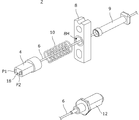
- FIG. 1 is a perspective view of a probe fitting structure 101 according to the first embodiment.
- FIG. 2 is a perspective view of the probe 2 before being assembled.
- FIG. 3 is an enlarged perspective view of the tip portion of the plunger 4.
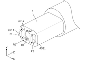
- FIG. 4A is an enlarged plan view of the base end portion PE of the plunger 4.
- FIG. 4B is a diagram showing a positional relationship between the protrusions P1 and P2 and the probe pin 18.
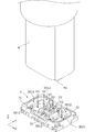
- FIG. 5 is a perspective view showing the connector 3 and a part of the plunger 4 facing the connector 3.
- FIG. 6 is a perspective view in which individual reference numerals are attached to the plurality of connection electrodes included in the connector 3.
- FIG. 7 is a vertical cross-sectional view showing the connector 3 and a part of the plunger 4 facing the connector 3.
- FIG. 8(A), 8(B), and 8(C) are vertical cross-sectional views showing each stage before and after the fitting of the probe plunger 4 to the connector 3.
- FIG. 9 is a perspective view of the tip of the plunger 4 of the probe according to the second embodiment.
- FIG. 10A is an enlarged plan view of the base end portion PE of the plunger 4.
- FIG. 10B is a diagram showing the positional relationship between the protrusions P1 and P2 and the probe pin 18.
- FIG. 11 is a perspective view of the connector 3 with which the plunger 4 shown in FIG. 9 is fitted.
- a probe fitting structure includes a connector to be inspected having a plurality of arranged connection electrodes, and a probe fitted to the connector, wherein the probe has a through hole. Having a flange for attaching the probe to an instrument, a coaxial cable that is inserted into the through hole and has a probe pin attached to the tip, a plunger that exposes the probe pin from the tip, the flange and the plunger And a spring having one end fixed to the flange and the other end fixed to the plunger, wherein the plunger is a plunger side formed at the tip of the plunger.
- the connector has a fitting portion, and the connector has a connector-side fitting portion that is fitted in contact with an outer surface of the plunger-side fitting portion.
- the plunger does not need a trumpet-like tapered portion with an opening that expands in the distal direction, so the planar size of the plunger can be equal to or smaller than the planar size of the connector. Therefore, it is not necessary to provide a space around the connector where other components are not mounted and arranged, and the component mounting density and the degree of integration of the circuit board are not reduced. In addition, it is possible to avoid interference and damage of components mounted near the connector.
- a probe fitting structure has a connector to be inspected having a plurality of arranged connection electrodes, and a probe fitted to the connector, and the probe has a through hole. Having a flange for attaching the probe to an instrument, a coaxial cable that is inserted into the through hole and has a probe pin attached to the tip, a plunger that exposes the probe pin from the tip, the flange and the plunger And a spring having one end fixed to the flange and the other end fixed to the plunger, wherein the plunger is a plunger side formed at the tip of the plunger.
- the connector has a fitting portion, and the connector has a connector-side fitting portion that surrounds and fits the plunger-side fitting portion.
- the plunger does not need a trumpet-like tapered portion with an opening that expands in the distal direction, so the planar size of the plunger can be equal to or smaller than the planar size of the connector. Therefore, it is not necessary to provide a space around the connector where other components are not mounted and arranged, and the component mounting density and the degree of integration of the circuit board are not reduced. In addition, it is possible to avoid interference and damage of components mounted near the connector.
- the connector has a plurality of connection electrodes with which the probe pins are in contact, and the plurality of connection electrodes are in the contact/separation direction of the probe.
- the probe pins are located at 180-degree rotational symmetry positions on the orthogonal plane, and the probe pins are respectively connected to different connection electrodes of the plurality of connection electrodes before and after the 180-degree rotation about the central axis of the 180-degree rotation of the connector. It is provided at the position where it abuts.
- the different contacting electrodes of the plurality of connecting electrodes of the connector are respectively brought into contact with each other. Does not overlap with the connection electrodes, and the number of connection pins can be increased as a result even though the number of probe pins is small.
- the connector has a plurality of connection electrodes, and the probe pins are a plurality of probe pins that are in contact with all of the plurality of connection electrodes. According to this structure, it is possible to measure all the connection electrodes in a single fitted state.
- the connector-side fitting portions are provided at a plurality of positions sandwiching the arrangement range of the plurality of connection electrodes, and the plunger-side fitting portion is fitted to the plurality of connector-side fitting portions. Fit each at the joint.
- the connector and the plunger can be fitted to each other at a plurality of dispersed locations, so that the fitting strength and the positional accuracy of the plunger with respect to the connector are improved.
- the plurality of connection electrodes form a row
- the plunger-side fitting portion has a shape along the row within the arrangement range of the plurality of connection electrodes. is there. According to this structure, the fitting portion between the connector and the plunger can be formed long, so that the fitting strength and the positional accuracy of the plunger with respect to the connector are improved.
- the plunger-side fitting portion is a protrusion
- the connector-side fitting portion is a recess into which the plunger-side fitting portion is inserted.
- the protruding portion has a cutout portion that secures a distance from the connection electrode or the holding portion of the connection electrode. According to this structure, interference between the plunger-side fitting portion and the connection electrode of the connector or the holding portion of the connection electrode is effectively prevented in the state where the plunger-side fitting portion is fitted to the connector-side fitting portion. ..
- both or one of the protrusion and the recess has an inclined portion whose thickness is smaller at the tip end portion than the base end portion in the insertion direction,
- the inclined portion guides the proper position of the protrusion with respect to the recess.
- a probe according to a ninth aspect of the present invention is a probe for inspecting a connector having a connection electrode, which has a flange having a through hole, a coaxial cable inserted into the through hole, and a flat base end.
- a plunger having a portion, and a probe pin attached to the coaxial cable, the tip of which is exposed from the base end portion, the plunger having a plurality of protrusions sandwiching the probe pin in a plan view of the base end portion.
- the length from the base end to the tips of the plurality of protrusions is longer than the length from the base to the tip of the probe pin.
- the above probe it is possible to prevent the probe pin from colliding with a member different from the electrode of the connector to be measured before the fitting. Moreover, the influence of noise from the outside can be suppressed.
- the probe pin is within a range surrounded by the outlines of the plurality of protrusions in a plan view of the base end portion of the plunger. According to this structure, it is possible to effectively prevent the probe pin from colliding with a member different from the electrode of the connector to be measured before fitting, and it is possible to effectively suppress the influence of noise from the outside. ..
- FIG. 1 is a perspective view of a probe fitting structure 101 according to the first embodiment.
- FIG. 2 is a perspective view of the probe 2 before being assembled.
- FIG. 3 is an enlarged perspective view of the tip portion of the plunger 4.
- the probe 2 is an inspection tool that is connected to the connector 3 mounted on the circuit board of the electronic device to inspect the characteristics of the electronic circuit connected to the connector 3.
- the connector 3 is a multipolar connector having a plurality of connection electrodes.
- the coaxial connector 12 is connected to the coaxial receptacle of the measuring instrument.
- the probe 2 includes a plunger 4, a coaxial cable 6, a spring 10, a flange 8, a connecting member 9 and a coaxial connector 12.
- the flange 8 has a through hole 8H, and the coaxial cable 6 is inserted into the through hole 8H.
- the connecting member 9 is a connecting member that connects the plunger 4 and the flange 8 via the spring 10.
- the plunger 4 is elastically held to the flange 8 via a spring 10.
- the plunger 4, the flange 8 and the connecting member 9 are all made of, for example, stainless steel, and the spring 10 is made of, for example, beryllium copper.
- a probe pin 18 and projections P1 and P2 are projected from the tip of the plunger.
- the “plunger tip surface” is the tip surface of the plunger 4 facing the connector 3.
- the probe pin 18 is a pin that is attached to the coaxial cable 6 and conducts to the inner conductor of the coaxial cable 6, and the outer conductor of the coaxial cable 6 conducts to the plunger 4.
- the protrusions P1 and P2 are features that correspond to the "plunger-side fitting portion" according to this invention.
- the part of the probe pin 18 that does not project from the tip of the plunger 4 has a coaxial structure by covering the space between the probe pin 18 and the plunger 4 with a bushing (resin member).
- the protrusion P1 has inclined portions 4S11 and 4S12
- the protrusion P2 has inclined portions 4S21 and 4S22.
- the operation of these inclined portions 4S11, 4S12, 4S21, 4S22 will be described later.
- the plunger includes a plurality of (two in this example) protrusions P1 and P2 sandwiching the probe pin 18 in a plan view of the base end portion PE.
- the length from the base end PE to the tips of the protrusions P1 and P2 is longer than the length from the base PE to the tip of the probe pin 18,
- FIG. 4A is an enlarged plan view of the base end portion PE of the plunger 4.
- FIG. 4B is a diagram showing a positional relationship between the protrusions P1 and P2 and the probe pin 18 in the base end PE.
- the outline OL of the two projections P1 and P2 is shown.
- a part of the probe pin 18 is within a range surrounded by the outlines OL of the plurality of projection portions (two in this example) P1 and P2.
- FIG. 5 is a perspective view showing the connector 3 and a part of the plunger 4 facing the connector 3.
- FIG. 7 is a vertical cross-sectional view showing the connector 3 and a part of the plunger 4 facing the connector 3.
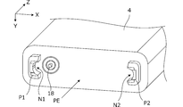
- the connector 3 has holes H1 and H2 into which the protrusions P1 and P2 of the plunger 4 shown in FIG. 3 fit.
- the holes H1 and H2 correspond to the "connector side fitting portion" according to the present invention.
- the projections P1 and P2 of the plunger 4 slide and fit on the metal frames 31 and 32 of the connector 3.
- the holes H1 and H2 of the connector 3 are brought into contact with and fitted to the outer side surfaces of the projections P1 and P2 of the plunger 4.
- the holes H1 and H2 of the connector 3 surround and fit the protrusions P1 and P2 of the plunger 4.
- the connector 3 is a molded body of metal material and resin. As shown in FIG. 5, the connector 3 has a plurality of connection electrodes 33 and metal frames 31 and 32. Although the metal frames 31 and 32 are continuous bodies, different reference numerals are given here for convenience of description.
- the metal frame 31 has inclined portions 3S11 and 3S12
- the metal frame 32 has inclined portions 3S21 and 3S22. The operation of these inclined portions 3S11, 3S12, 3S21, 3S22 will be described later.
- FIG. 6 is a perspective view in which a plurality of connection electrodes included in the connector 3 are given individual symbols.
- the plurality of connection electrodes 33 shown in FIG. 5 are composed of connection electrodes 33A, 33B, 33C, 33D, 33E, 33F, 33G, 33H.
- the connection electrodes 33A and 33F have a 180-degree rotational symmetry relationship in the plane (XY plane) orthogonal to the contact/separation direction (Z direction) of the probe 2.
- the connection electrodes 33C and 33D have a 180-degree rotational symmetry relationship.
- the connection electrodes 33B and 33E have a 180-degree rotational symmetry relationship.
- the connection electrodes 33G and 33H have a 180-degree rotational symmetry relationship.
- the probe pin 18 comes into contact with a predetermined connection electrode 33A of the plurality of connection electrodes of the connector 3 to be electrically conducted.
- FIG. 8A), 8(B), and 8(C) are vertical cross-sectional views showing respective stages before and after the fitting of the plunger 4 of the probe 2 to the connector 3.
- the protrusion P1 of the plunger 4 has an inclined portion 4S11
- the protrusion P2 has an inclined portion 4S21.
- the protrusions P1 and P2 are thinner at the tip end portion than at the base end portion.
- the inclined portion 4S11 is formed on the protrusion P1
- the inclined portion 4S21 is formed on the protrusion P2.
- the metal frame 31 of the connector 3 has an inclined portion 3S11
- the metal frame 32 has an inclined portion 3S21.
- Each of the inclined portions 3S11 and 3S21 is inclined in the direction in which the thickness becomes thinner at the tip end portion than the base end portions of the metal frames 31 and 32 of the connector 3.
- the state shown in FIG. 8(B) is obtained.
- the protrusion P2 of the plunger 4 contacts the metal frame 32 of the connector 3. That is, the protrusion P2 contacts the inclined portion 3S21 of the metal frame 32.
- the plunger 4 is lowered as it is, the protrusion P2 slides on the inclined portion 3S21 of the metal frame 32, and the plunger 4 receives a stress in the left direction in the direction shown in FIG. 8B.
- the convex portion of the metal frame 32 of the connector 3 contacts the inclined portion 4S21 of the protrusion P2, and the convex portion of the metal frame 31 contacts the inclined portion 4S11 of the protrusion P1. It stops in the state that it did. That is, in this state, the protrusions P1 and P2 of the plunger 4 fit into the holes H1 and H2 (see FIG. 5) of the connector 3. Then, the probe pin 18 protruding from the tip of the plunger 4 comes into contact with the connection electrode 33A and becomes electrically conductive. Thereby, the signal applied to or flowing through the connection electrode 33A can be inspected.
- the holes H1 and H2 include not only the inclined portions 3S11 and 3S21 inclined from the plane parallel to the YZ plane but also the inclined portions inclined from the plane parallel to the XZ plane. It also has parts 3S12 and 3S22. Therefore, the relative positions of the connector 3 and the plunger 4 in the in-plane direction parallel to the YZ plane are also guided. Therefore, both of the X direction and the Y direction of the plunger 4 with respect to the connector 3 are guided to the proper positional relationship, and the operability at the time of fitting is improved.
- the holes H1 and H2 of the connector 3 are formed at two positions sandwiching the arrangement range of the plurality of connection electrodes 33.
- the protrusions of No. 4 may fit into the grooves sandwiched by the rows in the arrangement range of the connection electrodes 33.
- the plurality of connection electrodes may form the two grooves G1 and G2, and the plunger 4 may be provided with a protrusion that fits into the two grooves G1 and G2. According to such a structure, the fitting portion between the connector 3 and the plunger 4 can be formed long, so that the fitting strength and the positional accuracy of the plunger 4 with respect to the connector 3 are improved.
- the probe 2 having the single probe pin 18 is used, but it may have a plurality of probe pins. Thereby, the probe pin can be brought into contact with each of the plurality of connection electrodes at the same time for measurement.
- the plurality of connection electrodes of the connector 3 are located at 180-degree rotational symmetry in the plane (XY plane) orthogonal to the contact/separation direction (Z direction) of the probe 2. Therefore, it is preferable that the fitting direction of the probe 2 with respect to the connector 3 be two ways in a 180-degree rotational relationship. In that case, in the two fitting states of the 180-degree rotational symmetry (first fitting state and second fitting state), different connection electrodes of the plurality of connection electrodes of the connector 3 are respectively brought into contact with each other. It is preferable that a plurality of probe pins be provided.
- a plurality of probe pins do not abut on the connection electrodes in the above-mentioned two fitted states, so that even a small number of probe pins can eventually abut on many connection electrodes. it can.
- the three probe pins can be connected to the connection electrodes 33D, in the second fitted state. It contacts 33E and 33F.
- the three probe pins can be connected to the connection electrodes 33D, 33B, and 33F in the second fitting state. Abut. In this way, since a large number of connection electrodes can be brought into contact with a small number of probe pins as a result, the adjacent space between the probe pins can be widened, and signal isolation between the probe pins can be easily ensured.
- the probe 2 may include a plurality of probe pins that abut on all of a plurality of connection electrodes. According to this configuration, it is possible to perform measurement on all the connection electrodes in a single fitted state.
- the second embodiment shows a probe in which the structure of the fitting portion between the plunger and the connector is different from that in the first embodiment.
- FIG. 9 is a perspective view of the tip of the plunger 4 of the probe according to the second embodiment.
- FIG. 10A is an enlarged plan view of the base end portion PE of the plunger 4.
- FIG. 10B is a diagram showing the positional relationship between the protrusions P1 and P2 and the probe pin 18.
- FIG. 11 is a perspective view of the connector 3 with which the plunger 4 shown in FIG. 9 is fitted.
- the probe pin 18 and the projections P1 and P2 respectively project from the tip of the plunger 4.
- the protrusions P1 and P2 are features that correspond to the "plunger-side fitting portion" according to this invention. Configurations other than those shown in FIGS. 9, 10, and 11 are as shown in the first embodiment.
- FIG. 10(B) the outline line OL of the two protrusions P1 and P2 is shown.
- all of the probe pins 18 are within a range surrounded by the outline line OL of the plurality of projection portions (two in this example) P1 and P2.
- the connector 3 has a connection electrode holding bar 34 that holds a plurality of connection electrodes 33 in a row. Recesses D1 and D2 are formed near both ends of the connection electrode holding bar 34.
- the protrusions P1 and P2 have notches N1 and N2, respectively. These cutout portions N1 and N2 are portions for ensuring a distance from the connection electrode 33 or the connection electrode holding bar 34.
- the connection electrode holding bar 34 corresponds to the "holding portion of the connection electrode" according to the present invention. That is, the protrusions P1 and P2 shown in FIG. 9 are connected to the protrusions P1 and P2, the connection electrode 33 or the connection electrode holding bar 34 in a state of being fitted into the recesses D1 and D2 of the connector 3 shown in FIG. A predetermined separation distance between them is ensured. Therefore, the protrusions P1 and P2 are not interfered with by the connection electrode holding bar 34. Moreover, since the protrusions P1 and P2 do not come close to the connection electrode 33 more than necessary, they do not adversely affect the electrical characteristics during measurement.
- the notches N1 and N2 are effective even if the projections P1 and P2 shown in FIG. 9 have a positional relationship such that they do not interfere with the connection electrode holding bar 34. That is, the risk that the projections P1 and P2 may hit the connection electrode holding bar 34 or the connection electrode 33 in the connector 3 and damage them during the operation (induction operation) during the fitting of the plunger 4 to the connector 3 is reduced. To be done.
- the notches N1 and N2 may have a shape and dimensions that sandwich both ends of the connection electrode holding bar 34 in the X direction or the Y direction. As a result, the fitting force of the plunger 4 with respect to the connector 3 can be increased.
- the recesses D1 and D2 of the connector 3 are formed at two positions sandwiching the arrangement range of the plurality of connection electrodes 33, but the plurality of connection electrodes form a row.
- the protrusion of the plunger 4 may be fitted in the groove along the row in the arrangement range of the connection electrodes 33.
- the grooves G1 and G2 are formed between the connection electrode holding bar 34 and the outer frame portion of the connector, and the projection portion that fits into one or both of the grooves G1 and G2 is formed by the plunger. 4 may be provided. According to such a structure, the fitting portion between the connector 3 and the plunger 4 can be formed long, so that the fitting strength and the positional accuracy of the plunger 4 with respect to the connector 3 are improved.
- the example in which the connector-side fitting portion and the plunger-side fitting portion are provided at positions of 180-degree rotational symmetry has been shown. Therefore, there are two ways of fitting the plunger 4 to the connector 3, 0 degree and 180 degrees. With this, by changing the direction of the plunger 4 with respect to the connector 3, the position of the connection electrode of the connector with which the probe pin 18 abuts can be selected.
- each of the plunger-side fitting portion and the connector-side fitting portion is not limited to two, but may be one or three or more.
- the connector-side fitting portion is the recesses such as the holes H1 and H2, the grooves G1 and G2, and the recesses D1 and D2, and the plunger-side fitting portion is the projections P1 and P2.
- the connector-side fitting portion may be a protrusion
- the plunger-side fitting portion may be a recessed portion such as a hole, groove, or recess that fits into the connector-side fitting portion.
Landscapes
- Physics & Mathematics (AREA)
- General Physics & Mathematics (AREA)
- Geometry (AREA)
- Measuring Leads Or Probes (AREA)
- Manufacturing Of Electrical Connectors (AREA)
- Details Of Connecting Devices For Male And Female Coupling (AREA)
Abstract
Description
配列された複数の接続電極を有する検査対象のコネクタと、前記コネクタに嵌合するプローブと、を有するプローブ嵌合構造であって、
前記プローブは、
貫通孔を有するフランジと、
前記貫通孔に挿通され、先端部にプローブピンを取り付けた同軸ケーブルと、
先端からプローブピンを露出させるプランジャと、
前記フランジと前記プランジャとの間で前記同軸ケーブルを内包し、一方端部が前記フランジに固定され、他方端部が前記プランジャに固定されたスプリングと、
を備え、
前記プランジャは、当該プランジャの先端部に形成されたプランジャ側嵌合部を有し、
前記コネクタは、前記プランジャ側嵌合部の外側面に接して嵌合するコネクタ側嵌合部を有する。
配列された複数の接続電極を有する検査対象のコネクタと、前記コネクタに嵌合するプローブと、を有するプローブ嵌合構造であって、
前記プローブは、
貫通孔を有するフランジと、
前記貫通孔に挿通され、先端部にプローブピンを取り付けた同軸ケーブルと、
先端からプローブピンを露出させるプランジャと、
前記フランジと前記プランジャとの間で前記同軸ケーブルを内包し、一方端部が前記フランジに固定され、他方端部が前記プランジャに固定されたスプリングと、
を備え、
前記プランジャは、当該プランジャの先端部に形成されたプランジャ側嵌合部を有し、
前記コネクタは、前記プランジャ側嵌合部を取り囲んで嵌合するコネクタ側嵌合部を有する。
接続電極を有するコネクタを検査するためのプローブであって、
貫通孔を有するフランジと、
前記貫通孔に挿通される同軸ケーブルと、
平面状の基端部を有するプランジャと、
前記同軸ケーブルに取り付けられ、先端が前記基端部から露出するプローブピンと、
を備え、
前記プランジャは、前記基端部の平面視で前記プローブピンを挟む複数の突起部を含み、
前記基端部から前記複数の突起部の先端までのそれぞれの長さは、前記基端部からプローブピンの先端までの長さよりも長い。
図1は第1の実施形態に係るプローブ嵌合構造101の斜視図である。図2はプローブ2の組立前の状態での斜視図である。図3はプランジャ4の先端部の拡大斜視図である。
図4(A)はプランジャ4の基端部PEの拡大平面図である。図4(B)は、基端部PEにおける突起部P1,P2とプローブピン18との位置関係を示す図である。図4(B)においては、2つの突起部P1,P2全体の外形線OLを示している。プランジャ4の基端部PEの平面視で、プローブピン18の一部は、複数の突起部(この例では2つの)突起部P1,P2全体の外形線OLで囲まれる範囲内にある。
第2の実施形態では、プランジャとコネクタとの嵌合部の構造が第1の実施形態とは異なるプローブについて示す。
G1,G2…溝
H1,H2…孔部
N1,N2…切り欠き部
P1,P2…突起部
2…プローブ
3…コネクタ
3S11,3S12…傾斜部
3S21,3S22…傾斜部
4…プランジャ
4S11,4S12…傾斜部
4S21,4S22…傾斜部
6…同軸ケーブル
8…フランジ
8H…貫通孔
9…連結部材
10…スプリング
12…同軸コネクタ
18…プローブピン
31,32…金属フレーム
33,33A~33H…接続電極
34…接続電極保持バー
101…プローブ嵌合構造
Claims (10)
- 配列された複数の接続電極を有する検査対象のコネクタと、前記コネクタに嵌合するプローブと、を有するプローブ嵌合構造であって、
前記プローブは、
貫通孔を有するフランジと、
前記貫通孔に挿通され、先端部にプローブピンを取り付けた同軸ケーブルと、
先端からプローブピンを露出させるプランジャと、
前記フランジと前記プランジャとの間で前記同軸ケーブルを内包し、一方端部が前記フランジに固定され、他方端部が前記プランジャに固定されたスプリングと、
を備え、
前記プランジャは、当該プランジャの先端部に形成されたプランジャ側嵌合部を有し、
前記コネクタは、前記プランジャ側嵌合部の外側面に接して嵌合するコネクタ側嵌合部を有する、
プローブ嵌合構造。 - 配列された複数の接続電極を有する検査対象のコネクタと、前記コネクタに嵌合するプローブと、を有するプローブ嵌合構造であって、
前記プローブは、
貫通孔を有するフランジと、
前記貫通孔に挿通され、先端部にプローブピンを取り付けた同軸ケーブルと、
先端からプローブピンを露出させるプランジャと、
前記フランジと前記プランジャとの間で前記同軸ケーブルを内包し、一方端部が前記フランジに固定され、他方端部が前記プランジャに固定されたスプリングと、
を備え、
前記プランジャは、当該プランジャの先端部に形成されたプランジャ側嵌合部を有し、
前記コネクタは、前記プランジャ側嵌合部を取り囲んで嵌合するコネクタ側嵌合部を有する、
プローブ嵌合構造。 - 前記プローブピンは複数あって、
前記コネクタは前記プローブピンが当接する複数の接続電極を有し、
前記複数の接続電極は、前記プローブの当接離間方向に対する直交面での180度回転対称の位置にあり、
前記複数のプローブピンは、前記コネクタの前記180度回転の中心軸に対して、180度回転の前後で、前記複数の接続電極のうちの異なる接続電極にそれぞれ当接する位置に設けられている、
請求項1又は2に記載のプローブ嵌合構造。 - 前記コネクタは複数の接続電極を有し、
前記プローブピンは、前記複数の接続電極の全てにそれぞれに当接する複数のプローブピンである、
請求項1又は2に記載のプローブ嵌合構造。 - 前記コネクタ側嵌合部は前記複数の接続電極の配列範囲を挟む複数箇所にあり、
前記プランジャ側嵌合部は前記複数のコネクタ側嵌合部にそれぞれ嵌合する、
請求項1又は2に記載のプローブ嵌合構造。 - 前記複数の接続電極は列を構成し、
前記プランジャ側嵌合部は前記複数の接続電極の配列範囲内の前記列に沿った形状である、
請求項1又は2に記載のプローブ嵌合構造。 - 前記プランジャ側嵌合部は突起部であり、前記コネクタ側嵌合部は前記プランジャ側嵌合部が挿入される陥凹部であり、前記突起部は、前記接続電極又は前記接続電極の保持部からの離間距離を確保する切り欠き部を有する、
請求項1から6のいずれかに記載のプローブ嵌合構造。 - 前記突起部及び前記陥凹部の双方に、又は一方に、挿入方向の基端部より先端部で厚みが薄くなる傾斜部を有し、当該傾斜部は前記陥凹部に対する前記突起部の適正位置を誘導する、請求項7に記載のプローブ嵌合構造。
- 接続電極を有するコネクタを検査するためのプローブであって、
貫通孔を有するフランジと、
前記貫通孔に挿通される同軸ケーブルと、
平面状の基端部を有するプランジャと、
前記同軸ケーブルに取り付けられ、先端が前記基端部から露出するプローブピンと、
を備え、
前記プランジャは、前記基端部の平面視で前記プローブピンを挟む複数の突起部を含み、
前記基端部から前記複数の突起部の先端までのそれぞれの長さは、前記基端部からプローブピンの先端までの長さよりも長い、
プローブ。 - 前記プランジャの前記基端部の平面視で、前記プローブピンは、前記複数の突起部全体の外形線で囲まれる範囲内にある、
請求項9に記載のプローブ。
Priority Applications (5)
| Application Number | Priority Date | Filing Date | Title |
|---|---|---|---|
| CN201980078176.XA CN113167813B (zh) | 2018-11-29 | 2019-11-22 | 探针嵌合构造以及探针 |
| JP2020557683A JP7243738B2 (ja) | 2018-11-29 | 2019-11-22 | プローブ嵌合構造 |
| KR1020217010554A KR102545546B1 (ko) | 2018-11-29 | 2019-11-22 | 프로브 끼워맞춤 구조 및 프로브 |
| TW108143688A TWI741422B (zh) | 2018-11-29 | 2019-11-29 | 探針嵌合構造及探針 |
| US17/331,336 US11719762B2 (en) | 2018-11-29 | 2021-05-26 | Probe fitting structure and probe |
Applications Claiming Priority (2)
| Application Number | Priority Date | Filing Date | Title |
|---|---|---|---|
| JP2018223627 | 2018-11-29 | ||
| JP2018-223627 | 2018-11-29 |
Related Child Applications (1)
| Application Number | Title | Priority Date | Filing Date |
|---|---|---|---|
| US17/331,336 Continuation US11719762B2 (en) | 2018-11-29 | 2021-05-26 | Probe fitting structure and probe |
Publications (1)
| Publication Number | Publication Date |
|---|---|
| WO2020110960A1 true WO2020110960A1 (ja) | 2020-06-04 |
Family
ID=70853340
Family Applications (1)
| Application Number | Title | Priority Date | Filing Date |
|---|---|---|---|
| PCT/JP2019/045857 Ceased WO2020110960A1 (ja) | 2018-11-29 | 2019-11-22 | プローブ嵌合構造及びプローブ |
Country Status (6)
| Country | Link |
|---|---|
| US (1) | US11719762B2 (ja) |
| JP (1) | JP7243738B2 (ja) |
| KR (1) | KR102545546B1 (ja) |
| CN (1) | CN113167813B (ja) |
| TW (1) | TWI741422B (ja) |
| WO (1) | WO2020110960A1 (ja) |
Cited By (2)
| Publication number | Priority date | Publication date | Assignee | Title |
|---|---|---|---|---|
| WO2022128253A1 (de) * | 2020-12-16 | 2022-06-23 | Lisa Dräxlmaier GmbH | Einzelkontaktierungseinrichtung für eine prüfvorrichtung zum durchgangsprüfen eines steckverbinders und prüfvorrichtung |
| JP2022116429A (ja) * | 2021-01-29 | 2022-08-10 | 株式会社村田製作所 | アダプタ |
Families Citing this family (3)
| Publication number | Priority date | Publication date | Assignee | Title |
|---|---|---|---|---|
| US11567102B2 (en) * | 2019-09-04 | 2023-01-31 | Chien Wen Chang | Auxiliary device for functional expansion and signal acquisition of testing system |
| WO2022163007A1 (ja) * | 2021-01-29 | 2022-08-04 | 株式会社村田製作所 | プローブ装置 |
| USD1067074S1 (en) * | 2023-06-03 | 2025-03-18 | Tempo Communications Inc. | Wire locator |
Citations (5)
| Publication number | Priority date | Publication date | Assignee | Title |
|---|---|---|---|---|
| JPS625280U (ja) * | 1985-06-25 | 1987-01-13 | ||
| JP2000162237A (ja) * | 1998-11-26 | 2000-06-16 | Fuji Photo Film Co Ltd | 基板検査装置 |
| JP2007263726A (ja) * | 2006-03-28 | 2007-10-11 | Furukawa Electric Co Ltd:The | コネクタ検査装置 |
| WO2016072193A1 (ja) * | 2014-11-07 | 2016-05-12 | 株式会社村田製作所 | プローブ |
| WO2018116568A1 (ja) * | 2016-12-22 | 2018-06-28 | 株式会社村田製作所 | プローブ構造 |
Family Cites Families (16)
| Publication number | Priority date | Publication date | Assignee | Title |
|---|---|---|---|---|
| US3063432A (en) * | 1961-01-13 | 1962-11-13 | Douglas R Bond | Water heater protection |
| JPS6095943A (ja) | 1983-10-31 | 1985-05-29 | Ibiden Co Ltd | プラグインパツケ−ジとその製造方法 |
| US4572113A (en) * | 1985-02-01 | 1986-02-25 | Baughman George W | Water leak control circuit |
| JPH0616075B2 (ja) * | 1985-06-21 | 1994-03-02 | 株式会社ヨコオ | 回路基板等の検査装置 |
| IT1273666B (it) * | 1994-07-20 | 1997-07-09 | Giuseppe Fugazza | Gruppo idraulico perfezionato per impianti misti di riscaldamento e acqua sanitaria |
| JPH0915448A (ja) * | 1995-06-26 | 1997-01-17 | Takahisa Jitsuno | 光ファイバコネクタ及びその製造方法 |
| JP3211932B2 (ja) * | 1995-08-02 | 2001-09-25 | 矢崎総業株式会社 | コネクタの検査方法およびコネクタ検査具 |
| DE19632604A1 (de) | 1996-08-13 | 1998-02-19 | Wilo Gmbh | Befülleinrichtung für Hydraulikbaugruppe |
| CN1851476A (zh) * | 2005-04-22 | 2006-10-25 | 安捷伦科技有限公司 | 接合器、以及使用其的半导体测试装置 |
| KR100650307B1 (ko) | 2005-10-14 | 2006-11-27 | 리노공업주식회사 | 동축 접촉 프로브 |
| KR101029697B1 (ko) * | 2007-03-20 | 2011-04-18 | 가부시키가이샤 니혼 마이크로닉스 | 전기적 접속장치 |
| JP5607934B2 (ja) * | 2008-02-01 | 2014-10-15 | 日本発條株式会社 | プローブユニット |
| CN201716340U (zh) * | 2009-04-13 | 2011-01-19 | 环旭电子股份有限公司 | 探针装置 |
| JP5370323B2 (ja) | 2010-09-22 | 2013-12-18 | 富士電機株式会社 | プローブユニット |
| JP5991823B2 (ja) * | 2012-02-14 | 2016-09-14 | 株式会社日本マイクロニクス | 電気的接続装置及びその組立方法 |
| JP5986391B2 (ja) * | 2012-02-17 | 2016-09-06 | シチズンファインデバイス株式会社 | コンタクトプローブを用いた検査装置 |
-
2019
- 2019-11-22 WO PCT/JP2019/045857 patent/WO2020110960A1/ja not_active Ceased
- 2019-11-22 JP JP2020557683A patent/JP7243738B2/ja active Active
- 2019-11-22 KR KR1020217010554A patent/KR102545546B1/ko active Active
- 2019-11-22 CN CN201980078176.XA patent/CN113167813B/zh active Active
- 2019-11-29 TW TW108143688A patent/TWI741422B/zh active
-
2021
- 2021-05-26 US US17/331,336 patent/US11719762B2/en active Active
Patent Citations (5)
| Publication number | Priority date | Publication date | Assignee | Title |
|---|---|---|---|---|
| JPS625280U (ja) * | 1985-06-25 | 1987-01-13 | ||
| JP2000162237A (ja) * | 1998-11-26 | 2000-06-16 | Fuji Photo Film Co Ltd | 基板検査装置 |
| JP2007263726A (ja) * | 2006-03-28 | 2007-10-11 | Furukawa Electric Co Ltd:The | コネクタ検査装置 |
| WO2016072193A1 (ja) * | 2014-11-07 | 2016-05-12 | 株式会社村田製作所 | プローブ |
| WO2018116568A1 (ja) * | 2016-12-22 | 2018-06-28 | 株式会社村田製作所 | プローブ構造 |
Cited By (4)
| Publication number | Priority date | Publication date | Assignee | Title |
|---|---|---|---|---|
| WO2022128253A1 (de) * | 2020-12-16 | 2022-06-23 | Lisa Dräxlmaier GmbH | Einzelkontaktierungseinrichtung für eine prüfvorrichtung zum durchgangsprüfen eines steckverbinders und prüfvorrichtung |
| CN116601510A (zh) * | 2020-12-16 | 2023-08-15 | 利萨·德雷克塞迈尔有限责任公司 | 用于插接连接器导通测试的测试设备的单个接触装置以及测试设备 |
| JP2022116429A (ja) * | 2021-01-29 | 2022-08-10 | 株式会社村田製作所 | アダプタ |
| JP7276363B2 (ja) | 2021-01-29 | 2023-05-18 | 株式会社村田製作所 | アダプタ |
Also Published As
| Publication number | Publication date |
|---|---|
| JP7243738B2 (ja) | 2023-03-22 |
| TWI741422B (zh) | 2021-10-01 |
| US11719762B2 (en) | 2023-08-08 |
| CN113167813A (zh) | 2021-07-23 |
| KR102545546B1 (ko) | 2023-06-20 |
| KR20210055763A (ko) | 2021-05-17 |
| CN113167813B (zh) | 2024-10-18 |
| JPWO2020110960A1 (ja) | 2021-10-07 |
| US20210278480A1 (en) | 2021-09-09 |
| TW202028753A (zh) | 2020-08-01 |
Similar Documents
| Publication | Publication Date | Title |
|---|---|---|
| JP7243738B2 (ja) | プローブ嵌合構造 | |
| CN110088632B (zh) | 探测器构造 | |
| JP4535828B2 (ja) | 検査ユニットの製法 | |
| US10948519B2 (en) | Probe | |
| JP5379474B2 (ja) | 導電性接触子ホルダ | |
| KR101415722B1 (ko) | 콘택트 프로브 및 프로브 유닛 | |
| TWM521829U (zh) | 纜線總成 | |
| US20130002281A1 (en) | Contact probe and probe unit | |
| JP2009156710A (ja) | 検査ソケット | |
| JP3226821U (ja) | 多極コネクタを測定するためのプローブ | |
| CN100435423C (zh) | 能够容易地进行接点电参数检查的连接器 | |
| JP2007178163A (ja) | 検査ユニットおよびそれに用いる検査プローブ用外皮チューブ組立体 | |
| JP3225841U (ja) | プローブをキャリブレーションするためのキャリブレーションアダプタ | |
| WO2023013413A1 (ja) | プローブカード | |
| JP4667253B2 (ja) | 四探針測定用同軸プローブ及びこれを備えたプローブ治具 | |
| US20170146568A1 (en) | Electronic test equipment | |
| KR102584652B1 (ko) | 전기 부품 검사 기구 | |
| JP2021162316A (ja) | 検査用ソケット | |
| TWI824790B (zh) | 連接器 | |
| JP4094617B2 (ja) | テストフィクスチャ | |
| JP2024106228A (ja) | 測定用プローブ及び当該測定用プローブを備えるプローブユニット | |
| JP2025011485A (ja) | 検査用プローブ | |
| JP2010019702A (ja) | プリント回路基板用測定装置 | |
| JP2023100074A (ja) | プローブ | |
| JP2020034359A (ja) | 検査システム |
Legal Events
| Date | Code | Title | Description |
|---|---|---|---|
| 121 | Ep: the epo has been informed by wipo that ep was designated in this application |
Ref document number: 19889046 Country of ref document: EP Kind code of ref document: A1 |
|
| ENP | Entry into the national phase |
Ref document number: 2020557683 Country of ref document: JP Kind code of ref document: A |
|
| ENP | Entry into the national phase |
Ref document number: 20217010554 Country of ref document: KR Kind code of ref document: A |
|
| NENP | Non-entry into the national phase |
Ref country code: DE |
|
| 122 | Ep: pct application non-entry in european phase |
Ref document number: 19889046 Country of ref document: EP Kind code of ref document: A1 |