WO2020116123A1 - 圧電積層体、圧電素子および圧電積層体の製造方法 - Google Patents
圧電積層体、圧電素子および圧電積層体の製造方法 Download PDFInfo
- Publication number
- WO2020116123A1 WO2020116123A1 PCT/JP2019/044775 JP2019044775W WO2020116123A1 WO 2020116123 A1 WO2020116123 A1 WO 2020116123A1 JP 2019044775 W JP2019044775 W JP 2019044775W WO 2020116123 A1 WO2020116123 A1 WO 2020116123A1
- Authority
- WO
- WIPO (PCT)
- Prior art keywords
- film
- piezoelectric
- substrate
- knn
- light transmittance
- Prior art date
- Legal status (The legal status is an assumption and is not a legal conclusion. Google has not performed a legal analysis and makes no representation as to the accuracy of the status listed.)
- Ceased
Links
Images


Classifications
-
- H—ELECTRICITY
- H03—ELECTRONIC CIRCUITRY
- H03H—IMPEDANCE NETWORKS, e.g. RESONANT CIRCUITS; RESONATORS
- H03H3/00—Apparatus or processes specially adapted for the manufacture of impedance networks, resonating circuits, resonators
- H03H3/007—Apparatus or processes specially adapted for the manufacture of impedance networks, resonating circuits, resonators for the manufacture of electromechanical resonators or networks
- H03H3/02—Apparatus or processes specially adapted for the manufacture of impedance networks, resonating circuits, resonators for the manufacture of electromechanical resonators or networks for the manufacture of piezoelectric or electrostrictive resonators or networks
-
- H—ELECTRICITY
- H10—SEMICONDUCTOR DEVICES; ELECTRIC SOLID-STATE DEVICES NOT OTHERWISE PROVIDED FOR
- H10N—ELECTRIC SOLID-STATE DEVICES NOT OTHERWISE PROVIDED FOR
- H10N30/00—Piezoelectric or electrostrictive devices
- H10N30/80—Constructional details
- H10N30/85—Piezoelectric or electrostrictive active materials
- H10N30/853—Ceramic compositions
- H10N30/8542—Alkali metal based oxides, e.g. lithium, sodium or potassium niobates
-
- C—CHEMISTRY; METALLURGY
- C01—INORGANIC CHEMISTRY
- C01G—COMPOUNDS CONTAINING METALS NOT COVERED BY SUBCLASSES C01D OR C01F
- C01G33/00—Compounds of niobium
- C01G33/006—Compounds containing niobium, with or without oxygen or hydrogen, and containing two or more other elements
-
- C—CHEMISTRY; METALLURGY
- C23—COATING METALLIC MATERIAL; COATING MATERIAL WITH METALLIC MATERIAL; CHEMICAL SURFACE TREATMENT; DIFFUSION TREATMENT OF METALLIC MATERIAL; COATING BY VACUUM EVAPORATION, BY SPUTTERING, BY ION IMPLANTATION OR BY CHEMICAL VAPOUR DEPOSITION, IN GENERAL; INHIBITING CORROSION OF METALLIC MATERIAL OR INCRUSTATION IN GENERAL
- C23C—COATING METALLIC MATERIAL; COATING MATERIAL WITH METALLIC MATERIAL; SURFACE TREATMENT OF METALLIC MATERIAL BY DIFFUSION INTO THE SURFACE, BY CHEMICAL CONVERSION OR SUBSTITUTION; COATING BY VACUUM EVAPORATION, BY SPUTTERING, BY ION IMPLANTATION OR BY CHEMICAL VAPOUR DEPOSITION, IN GENERAL
- C23C14/00—Coating by vacuum evaporation, by sputtering or by ion implantation of the coating forming material
- C23C14/06—Coating by vacuum evaporation, by sputtering or by ion implantation of the coating forming material characterised by the coating material
- C23C14/08—Oxides
- C23C14/088—Oxides of the type ABO3 with A representing alkali, alkaline earth metal or Pb and B representing a refractory or rare earth metal
-
- C—CHEMISTRY; METALLURGY
- C23—COATING METALLIC MATERIAL; COATING MATERIAL WITH METALLIC MATERIAL; CHEMICAL SURFACE TREATMENT; DIFFUSION TREATMENT OF METALLIC MATERIAL; COATING BY VACUUM EVAPORATION, BY SPUTTERING, BY ION IMPLANTATION OR BY CHEMICAL VAPOUR DEPOSITION, IN GENERAL; INHIBITING CORROSION OF METALLIC MATERIAL OR INCRUSTATION IN GENERAL
- C23C—COATING METALLIC MATERIAL; COATING MATERIAL WITH METALLIC MATERIAL; SURFACE TREATMENT OF METALLIC MATERIAL BY DIFFUSION INTO THE SURFACE, BY CHEMICAL CONVERSION OR SUBSTITUTION; COATING BY VACUUM EVAPORATION, BY SPUTTERING, BY ION IMPLANTATION OR BY CHEMICAL VAPOUR DEPOSITION, IN GENERAL
- C23C14/00—Coating by vacuum evaporation, by sputtering or by ion implantation of the coating forming material
- C23C14/58—After-treatment
- C23C14/5806—Thermal treatment
-
- H—ELECTRICITY
- H03—ELECTRONIC CIRCUITRY
- H03H—IMPEDANCE NETWORKS, e.g. RESONANT CIRCUITS; RESONATORS
- H03H3/00—Apparatus or processes specially adapted for the manufacture of impedance networks, resonating circuits, resonators
- H03H3/007—Apparatus or processes specially adapted for the manufacture of impedance networks, resonating circuits, resonators for the manufacture of electromechanical resonators or networks
- H03H3/02—Apparatus or processes specially adapted for the manufacture of impedance networks, resonating circuits, resonators for the manufacture of electromechanical resonators or networks for the manufacture of piezoelectric or electrostrictive resonators or networks
- H03H3/04—Apparatus or processes specially adapted for the manufacture of impedance networks, resonating circuits, resonators for the manufacture of electromechanical resonators or networks for the manufacture of piezoelectric or electrostrictive resonators or networks for obtaining desired frequency or temperature coefficient
-
- H—ELECTRICITY
- H03—ELECTRONIC CIRCUITRY
- H03H—IMPEDANCE NETWORKS, e.g. RESONANT CIRCUITS; RESONATORS
- H03H9/00—Networks comprising electromechanical or electro-acoustic elements; Electromechanical resonators
- H03H9/02—Details
- H03H9/02007—Details of bulk acoustic wave devices
- H03H9/02015—Characteristics of piezoelectric layers, e.g. cutting angles
- H03H9/02031—Characteristics of piezoelectric layers, e.g. cutting angles consisting of ceramic
-
- H—ELECTRICITY
- H03—ELECTRONIC CIRCUITRY
- H03H—IMPEDANCE NETWORKS, e.g. RESONANT CIRCUITS; RESONATORS
- H03H9/00—Networks comprising electromechanical or electro-acoustic elements; Electromechanical resonators
- H03H9/02—Details
- H03H9/02535—Details of surface acoustic wave devices
- H03H9/02543—Characteristics of substrate, e.g. cutting angles
- H03H9/02574—Characteristics of substrate, e.g. cutting angles of combined substrates, multilayered substrates, piezoelectrical layers on not-piezoelectrical substrate
-
- H—ELECTRICITY
- H10—SEMICONDUCTOR DEVICES; ELECTRIC SOLID-STATE DEVICES NOT OTHERWISE PROVIDED FOR
- H10N—ELECTRIC SOLID-STATE DEVICES NOT OTHERWISE PROVIDED FOR
- H10N30/00—Piezoelectric or electrostrictive devices
- H10N30/01—Manufacture or treatment
- H10N30/04—Treatments to modify a piezoelectric or electrostrictive property, e.g. polarisation characteristics, vibration characteristics or mode tuning
-
- H—ELECTRICITY
- H10—SEMICONDUCTOR DEVICES; ELECTRIC SOLID-STATE DEVICES NOT OTHERWISE PROVIDED FOR
- H10N—ELECTRIC SOLID-STATE DEVICES NOT OTHERWISE PROVIDED FOR
- H10N30/00—Piezoelectric or electrostrictive devices
- H10N30/01—Manufacture or treatment
- H10N30/07—Forming of piezoelectric or electrostrictive parts or bodies on an electrical element or another base
- H10N30/074—Forming of piezoelectric or electrostrictive parts or bodies on an electrical element or another base by depositing piezoelectric or electrostrictive layers, e.g. aerosol or screen printing
- H10N30/076—Forming of piezoelectric or electrostrictive parts or bodies on an electrical element or another base by depositing piezoelectric or electrostrictive layers, e.g. aerosol or screen printing by vapour phase deposition
-
- H—ELECTRICITY
- H10—SEMICONDUCTOR DEVICES; ELECTRIC SOLID-STATE DEVICES NOT OTHERWISE PROVIDED FOR
- H10N—ELECTRIC SOLID-STATE DEVICES NOT OTHERWISE PROVIDED FOR
- H10N30/00—Piezoelectric or electrostrictive devices
- H10N30/704—Piezoelectric or electrostrictive devices based on piezoelectric or electrostrictive films or coatings
-
- C—CHEMISTRY; METALLURGY
- C01—INORGANIC CHEMISTRY
- C01P—INDEXING SCHEME RELATING TO STRUCTURAL AND PHYSICAL ASPECTS OF SOLID INORGANIC COMPOUNDS
- C01P2002/00—Crystal-structural characteristics
- C01P2002/30—Three-dimensional structures
- C01P2002/34—Three-dimensional structures perovskite-type (ABO3)
-
- C—CHEMISTRY; METALLURGY
- C01—INORGANIC CHEMISTRY
- C01P—INDEXING SCHEME RELATING TO STRUCTURAL AND PHYSICAL ASPECTS OF SOLID INORGANIC COMPOUNDS
- C01P2002/00—Crystal-structural characteristics
- C01P2002/50—Solid solutions
- C01P2002/52—Solid solutions containing elements as dopants
- C01P2002/54—Solid solutions containing elements as dopants one element only
-
- C—CHEMISTRY; METALLURGY
- C01—INORGANIC CHEMISTRY
- C01P—INDEXING SCHEME RELATING TO STRUCTURAL AND PHYSICAL ASPECTS OF SOLID INORGANIC COMPOUNDS
- C01P2006/00—Physical properties of inorganic compounds
- C01P2006/40—Electric properties
-
- C—CHEMISTRY; METALLURGY
- C01—INORGANIC CHEMISTRY
- C01P—INDEXING SCHEME RELATING TO STRUCTURAL AND PHYSICAL ASPECTS OF SOLID INORGANIC COMPOUNDS
- C01P2006/00—Physical properties of inorganic compounds
- C01P2006/60—Optical properties, e.g. expressed in CIELAB-values
-
- H—ELECTRICITY
- H10—SEMICONDUCTOR DEVICES; ELECTRIC SOLID-STATE DEVICES NOT OTHERWISE PROVIDED FOR
- H10N—ELECTRIC SOLID-STATE DEVICES NOT OTHERWISE PROVIDED FOR
- H10N30/00—Piezoelectric or electrostrictive devices
- H10N30/01—Manufacture or treatment
- H10N30/07—Forming of piezoelectric or electrostrictive parts or bodies on an electrical element or another base
- H10N30/072—Forming of piezoelectric or electrostrictive parts or bodies on an electrical element or another base by laminating or bonding of piezoelectric or electrostrictive bodies
- H10N30/073—Forming of piezoelectric or electrostrictive parts or bodies on an electrical element or another base by laminating or bonding of piezoelectric or electrostrictive bodies by fusion of metals or by adhesives
-
- H—ELECTRICITY
- H10—SEMICONDUCTOR DEVICES; ELECTRIC SOLID-STATE DEVICES NOT OTHERWISE PROVIDED FOR
- H10N—ELECTRIC SOLID-STATE DEVICES NOT OTHERWISE PROVIDED FOR
- H10N30/00—Piezoelectric or electrostrictive devices
- H10N30/80—Constructional details
- H10N30/87—Electrodes or interconnections, e.g. leads or terminals
- H10N30/877—Conductive materials
- H10N30/878—Conductive materials the principal material being non-metallic, e.g. oxide or carbon based
Definitions
- the present invention relates to a piezoelectric laminate, a piezoelectric element, and a method for manufacturing a piezoelectric laminate.
- Piezoelectric materials are widely used in functional electronic parts such as sensors and actuators.
- As the material of the piezoelectric body for example, potassium sodium niobate (KNN) may be used (see, for example, Patent Documents 1 and 2).
- KNN potassium sodium niobate
- An object of the present invention is to provide a piezoelectric film with improved versatility and its related technology.
- Board An electrode film, A piezoelectric film made of alkali niobium oxide having a perovskite structure represented by a composition formula (K 1-x Na x )NbO 3 (0 ⁇ x ⁇ 1), Provided are a piezoelectric laminate having an average light transmittance of 65% or more in the visible light and near-infrared wavelength regions of the piezoelectric film, and a related technique thereof.
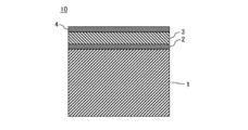
- FIG. 3 is a schematic diagram showing a state where the piezoelectric laminated body 10 is obtained by separation. It is a figure which shows an example of the cross-section of the piezoelectric laminated body 10 concerning the modification of this invention.
- a laminated body (laminated substrate) 10 (hereinafter, also referred to as a piezoelectric laminated body 10) having a piezoelectric film according to the present embodiment includes a substrate 1 and a substrate 1.
- the lower electrode film 2 formed on the lower electrode film 2, the piezoelectric film (piezoelectric thin film) 3 formed on the lower electrode film 2, and the upper electrode film 4 formed on the piezoelectric film 3.
- the substrate 1 is a substrate (transparent substrate) having a light transmittance of, for example, 65% or more at least in the visible light wavelength region (about 380 to 800 nm), preferably in the visible light and near infrared wavelength region (380 to 1,400 nm). ) Is preferably used.
- the substrate for example, strontium titanate (SrTiO 3 , abbreviated as STO) substrate, quartz glass (SiO 2 ) substrate, sapphire (Al 2 O 3 ) substrate, gallium nitride (GaN) substrate, gallium oxide (Ga 2 O 3 ) substrate
- the thickness of the substrate 1 is, for example, 300 to 1,000 ⁇ m.
- the lower electrode film 2 is preferably composed of an electrode (transparent electrode) having a light transmittance of, for example, 65% or more at least in the visible light wavelength region, preferably in the visible light and near-infrared wavelength regions.
- the lower electrode film 2 can be formed using a metal oxide such as strontium ruthenate (SrRuO 3 , abbreviated: SRO), lanthanum nickelate (LaNiO 3 , abbreviated: LNO).
- SRO strontium ruthenate
- LaNiO 3 lanthanum nickelate
- LNO lanthanum nickelate
- the lower electrode film 2 is a single crystal film or a polycrystalline film. When the lower electrode film 2 is formed using SRO, it is preferable that the crystals forming the lower electrode film 2 (SRO film) are preferentially oriented in the (100) plane orientation with respect to the surface of the substrate 1.
- the surface of the SRO film (the surface that is the base of the piezoelectric film 3) is mainly composed of the SRO (100) surface.
- the lower electrode film 2 can be formed by a method such as a sputtering method or a vapor deposition method.
- the lower electrode film 2 may be formed using indium oxide such as indium tin oxide (ITO), indium zinc oxide (IZO), and indium gallium zinc oxide (IGZO) in addition to SRO and LNO. it can.
- the thickness of the lower electrode film 2 is, for example, 10 to 400 nm.
- the lower electrode film 2 may be a thin film (metal thin film) formed by using various metals such as platinum (Pt) and gold (Au) and alloys containing these as the main components.
- Pt platinum
- Au gold
- the lower electrode film 2 is preferable that the lower electrode film 2 (Pt film) is preferentially oriented in the (111) plane direction with respect to the surface of the substrate 1. That is, the surface of the Pt film is preferably composed of the Pt(111) plane.
- the lower electrode film 2 (Pt film) can be formed by a method such as a sputtering method or a vapor deposition method.
- the thickness of the lower electrode film 2 (Pt film) is, for example, 1 to 10 nm, preferably 2 to 5 nm.
- the piezoelectric film 3 contains, for example, potassium (K), sodium (Na), and niobium (Nb), and is an alkaline niobium oxide represented by a composition formula (K 1-x Na x )Nb y O 3 , that is, niobium.
- the film can be formed using potassium sodium acidate (KNN).
- the piezoelectric film 3 is a KNN polycrystalline film (hereinafter, also referred to as a KNN film 3).
- the crystal structure of KNN is a perovskite structure.
- the crystal forming the KNN film 3 is preferably preferentially oriented in the (001) plane orientation with respect to the surface of the substrate 1. That is, it is preferable that the surface of the KNN film 3 (the surface serving as the base of the upper electrode film 4) is mainly composed of the KNN (001) surface.
- the crystal forming the KNN film 3 can be easily oriented in the (001) plane orientation with respect to the surface of the substrate 1.
- the crystals forming the KNN film 3 are oriented in the (001) plane orientation with respect to the surface of the substrate 1, and 80% or more of the surface of the KNN film 3 is KNN(001). ) It becomes possible to be a surface.
- the thickness of the KNN film 3 is, for example, 0.1 to 10 ⁇ m.
- the KNN film 3 can be formed by a method such as a sputtering method, a PLD (Pulsed Laser Deposition) method, a sol-gel method or the like.
- the composition ratio of the KNN film 3 can be adjusted, for example, by controlling the composition of the target material used during sputtering film formation.
- the target material can be produced, for example, by mixing and firing K 2 CO 3 powder, Na 2 CO 3 powder, Nb 2 O 5 powder, or the like.
- the composition of the target material can be controlled by adjusting the mixing ratio of K 2 CO 3 powder, Na 2 CO 3 powder, Nb 2 O 5 powder and the like.
- the KNN film 3 has optical transparency (transparency).
- the KNN film 3 has an average light transmittance of 65% or more in the visible light and near-infrared wavelength range (380 to 1,400 nm).
- the average light transmittance of the KNN film 3 in the visible light wavelength region (380 to 800 nm) is, for example, 56% or more.
- the upper limit of the average light transmittance is not particularly limited, and the upper limit is preferably 100%. However, at the current state of the art, the upper limit of the average light transmittance of the KNN film 3 in the visible and near infrared wavelength regions is about 75%.
- the average light transmittance is the average value of the light transmittance of the KNN film 3 in a predetermined wavelength region (range).
- the light transmittance of the KNN film 3 can be measured by a known light transmittance measuring device.
- the light transmittance of the KNN film is measured by a spectroscopic ellipsometer (JA-Woollam, M-2000).
- the average light transmittance of the KNN film 3 in the wavelength range of violet visible light (380 nm or more and less than 450 nm) is preferably 39.5% or more and 39.9% or less.
- the average light transmittance of the KNN film 3 in the wavelength region of blue visible light (450 nm or more and less than 495 nm) is preferably 48.5% or more and 54% or less.
- the average light transmittance of the KNN film 3 in the wavelength region of green visible light (495 nm or more and less than 570 nm) is preferably 55% or more and 61.5% or less.
- the average light transmittance of the KNN film 3 in the yellow visible light wavelength region (570 nm or more and less than 590 nm) is preferably 58.5% or more and 65% or less.
- the average light transmittance of the KNN film 3 in the orange visible light wavelength region (590 nm or more and less than 620 nm) is preferably 60% or more and 66.5% or less.
- the average light transmittance of the KNN film 3 in the wavelength region of red visible light (620 nm or more and less than 750 nm) is preferably 63.5% or more and 70% or less.
- the average light transmittance of the KNN film 3 in the wavelength region of violet visible light (750 nm or more and 800 nm or less) is preferably 66.5% or more and 71.5% or less.
- a mixed gas (Ar/O 2 mixed gas) of, for example, an argon (Ar) gas and an oxygen (O 2 ) gas is used as an atmospheric gas when the KNN film 3 is formed by sputtering.
- the partial pressure of water (H 2 O partial pressure) contained in the Ar/O 2 mixed gas during sputtering film formation may be increased, or after the KNN film 3 is formed, It is effective to heat-treat the KNN film 3 in the air or an oxygen-containing atmosphere before forming the upper electrode film 4 described later. With these, the KNN film 3 can be sufficiently oxidized, and oxygen vacancies in the KNN film 3 can be reduced. As a result, the light transmittance of the KNN film 3 can be increased.
- the light transmittance of the KNN film 3 can be set within the above range.
- the heat treatment is preferably performed at a temperature equal to or higher than the film forming temperature of the KNN film 3.
- the light transmittance of the KNN film 3 can be set within the above range by setting the H 2 O partial pressure at the time of forming the KNN film 3 to 0.05 Pa or more.
- the KNN film 3 preferably contains a metal element selected from the group consisting of copper (Cu) and manganese (Mn) at a concentration within the range of 0.2 to 2.0 at %.
- the film characteristics of the KNN film 3 can be improved by adding at least one of Cu and Mn in the KNN film 3 within the above-mentioned concentration range.
- the insulating property (leak resistance) of the KNN film 3 can be enhanced, and the relative dielectric constant of the KNN film 3 can be set to a suitable size according to the application of the piezoelectric laminated body 10.
- a fluorine-based etching solution for example, hydrogen fluoride (HF) and ammonium fluoride (NH 4 F) is added, respectively).
- BHF buffered hydrofluoric acid
- the light transmittance of the KNN film 3 tends to decrease.
- the film forming atmosphere of the KNN film 3 is as described above.
- the light transmittance of the KNN film 3 can be set within the above range by increasing the H 2 O partial pressure in the inside or by performing heat treatment after forming the KNN film 3.
- the relative dielectric constant of the KNN film 3 does not become excessive, and the sensitivity is lowered when the piezoelectric laminate 10 is applied to, for example, a sensor.
- the addition amount of Cu or Mn is appropriate and it is difficult to preferentially orient the crystals forming the KNN film 3 in the (001) plane orientation with respect to the surface of the substrate 1. Be done. Even when the H 2 O partial pressure in the atmosphere for forming the KNN film 3 is increased or the heat treatment is performed after forming the KNN film 3, the light transmittance of the KNN film 3 falls within the above range. Tend to be able to.
- the KNN film 3 can maintain elements such as lithium (Li), Ta and antimony (Sb) other than K, Na, Nb, Cu and Mn in the light transmittance of the KNN film 3 within the above range. It may be contained at a concentration of, for example, 5 at% or less.
- elements such as lithium (Li), Ta and antimony (Sb) other than K, Na, Nb, Cu and Mn in the light transmittance of the KNN film 3 within the above range. It may be contained at a concentration of, for example, 5 at% or less.
- the upper electrode film 4 is preferably composed of an electrode (transparent electrode) having a light transmittance of, for example, 65% or more at least in the visible light wavelength region, preferably in the visible light and near infrared wavelength regions.
- the upper electrode film 4 can be formed using a metal oxide such as SRO or LNO, or an indium oxide such as ITO, IZO or IGZO.
- the upper electrode film 4 does not greatly affect the crystal structure of the KNN film 3, unlike the lower electrode film 2. Therefore, the crystal structure of the upper electrode film 4 and the film forming method are not particularly limited.
- the upper electrode film 4 can be formed by a method such as a sputtering method, a vapor deposition method, a plating method, a metal paste method or the like.
- the thickness of the upper electrode film 4 is, for example, 3 to 1,000 nm. Further, the upper electrode film 4 may be a thin film (metal thin film) formed by using various metals such as Pt and Au, or alloys containing these as the main components. When the upper electrode film 4 is formed using Pt, Au or the like, the thickness of the upper electrode film 4 is, for example, 1 to 10 nm, preferably 2 to 5 nm. Further, the upper electrode film 4 may be a thin wire (metal thin wire) formed by using various metals such as Pt and Au, and alloys containing these as the main components.
- the piezoelectric laminated body 10 includes the substrate 1 (transparent substrate), the lower electrode film 2 (transparent electrode), the transparent KNN film 3 and the upper electrode film 4 (transparent electrode), so that the piezoelectric laminated body 10 is
- the overall light transmittance (average light transmittance) in at least the visible light wavelength region, preferably in the visible light and near-infrared wavelength region, can be 50% or more, and preferably 60% or more.
- FIG. 2 shows a schematic configuration diagram of the piezoelectric device 30 in the present embodiment.
- the piezoelectric device 30 is configured to include at least a piezoelectric element 20 obtained by molding the above-described piezoelectric laminated body 10 into a predetermined shape, and voltage detection means 11a or voltage application means 11b connected to the piezoelectric element 20. It
- the piezoelectric device 30 can function as a sensor.
- the deformation generates a voltage between the lower electrode film 2 and the upper electrode film 4.
- the piezoelectric device 30 can be suitably used for applications that require a light transmissive property (transparency).
- the piezoelectric device 30 can be suitably used as a sensor for a touch panel or a display of a mobile phone.
- the piezoelectric device 30 By connecting the voltage applying means 11b between the lower electrode film 2 and the upper electrode film 4 of the piezoelectric element 20, the piezoelectric device 30 can function as an actuator. By applying a voltage between the lower electrode film 2 and the upper electrode film 4 by the voltage applying means 11b, the KNN film 3 can be deformed. By this deforming operation, various members connected to the piezoelectric device 30 can be operated.
- the lower electrode film 2 is formed on one of the main surfaces of the substrate 1.
- the KNN film 3 is formed on the lower electrode film 2 by using, for example, the RF sputtering method.
- the KNN film 3 is heat-treated.
- the upper electrode film 4 is formed on the KNN film 3 after the heat treatment by using, for example, the RF sputtering method.
- a piezoelectric element 20 is obtained by forming the piezoelectric laminate 10 into a predetermined shape by etching or the like, and a piezoelectric device 30 is obtained by connecting the voltage detecting means 11a or the voltage applying means 11b to the piezoelectric element 20.
- the following conditions are exemplified as the conditions for forming the lower electrode film 2, the KNN film 3, and the upper electrode film 4, and the heat treatment conditions for the KNN film 3.
- Temperature film forming temperature, eg substrate temperature: Room temperature (about 27° C.) to 500° C., preferably 150 to 250° C., more preferably about 200° C.
- Discharge power 100 to 500 W, preferably 200 to 400 W
- Introduced gas Ar gas Ar gas atmosphere pressure: 1 to 10 Pa, preferably 3 to 5 Pa
- Film formation time 3 to 10 minutes, preferably 5 to 6 minutes
- Temperature film forming temperature, eg substrate temperature: 100 to 500°C, preferably 200 to 400°C Discharge power: 1,000 to 1,500 W, preferably 1,200 to 1,300 W
- Processing atmosphere Ar gas atmosphere
- Atmospheric pressure 0.1 to 0.5 Pa, preferably 0.2 to 0.4 Pa
- Processing time 30 seconds to 2 minutes, preferably about 1 minute
- Temperature film forming temperature, eg substrate temperature: 500 to 700° C., preferably 600° C.
- Discharge power 2,000 to 2,400 W, preferably 2,200 W
- Introduced gas Ar+O 2 mixed gas
- Ar+O 2 mixed gas atmosphere pressure 0.2 to 0.5 Pa, preferably 0.25 to 0.4 Pa
- Partial pressure of Ar gas with respect to O 2 gas Ar/O 2 partial pressure ratio: 30/1 to 20/1, preferably 27/1 to 23/1
- Film formation rate 0.5 to 2 ⁇ m/hr, preferably 1 to 1.5 ⁇ m/hr
- Atmosphere Air or oxygen-containing atmosphere
- Temperature 600 to 1,000° C., preferably 650 to 900° C., more preferably a temperature within the above range and higher than the treatment temperature of the KNN film
- Heat treatment time KNN film thickness 0.5 ⁇ m or more per 1 ⁇ m, preferably 24 hours or more, more preferably 40 hours or more
- the partial pressure of H 2 O in the atmosphere for forming the KNN film 3 may be increased.
- the light transmittance of the KNN film 3 can be increased as in the case where the above heat treatment is performed.
- the partial pressure of H 2 O in the atmosphere for forming the KNN film 3 may be increased, and the heat treatment may be performed on the KNN film 3 after the formation of the KNN film 3 and before the formation of the upper electrode 4. Thereby, the light transmittance of the KNN film 3 can be further increased.
- etching method for forming the piezoelectric laminated body 10 into a predetermined shape by etching or the like for example, a dry etching method such as reactive ion etching or a wet etching method using a predetermined etching liquid can be used.
- a photoresist pattern as an etching mask for dry etching is formed on the piezoelectric laminate 10 (the upper electrode film 4 and the KNN film 3 when the upper electrode film 4 is not provided) by photolithography. It is formed by a lithography process or the like.
- a noble metal film such as a chromium (Cr) film, a nickel (Ni) film, a platinum (Pt) film, or a Ti film may be formed by a sputtering method.
- etching is performed on the piezoelectric laminate 10 (the upper electrode film 4, the KNN film 3, etc.) using a gas containing a halogen element as an etching gas.
- the halogen element includes chlorine (Cl), fluorine (F), and the like.
- BCl 3 gas, SiCl 4 gas, chlorine (Cl 2 ) gas, CF 4 gas, C 4 F 8 gas, or the like can be used as the gas containing a halogen element.
- the piezoelectric laminated body 10 When the piezoelectric laminated body 10 is formed by wet etching, silicon oxide (SiO x as an etching mask for the wet etching is formed on the piezoelectric laminated body 10 (the upper electrode film 4 and the KNN film 3 when the upper electrode film 4 is not provided)). ) Form a film or the like. Then, for example, the piezoelectric laminate 10 is immersed in an etching solution containing an alkaline aqueous solution of a chelating agent and containing no hydrofluoric acid, and the piezoelectric laminate 10 (the upper electrode film 4, the KNN film 3, etc.) is wet-etched.
- silicon oxide SiO x as an etching mask for the wet etching
- etching solution containing an alkaline aqueous solution of a chelating agent and containing no hydrofluoric acid an etching solution obtained by mixing ethylenediaminetetraacetic acid as a chelating agent, ammonia water, and hydrogen peroxide solution can be used.
- the KNN film 3 according to this embodiment has an average light transmittance of 65% or more in the visible light and near-infrared wavelength regions. Since the KNN film 3 has a light-transmitting property as described above, the transparent substrate is used as the substrate 1 and the transparent electrodes are used as the lower electrode film 2 and the upper electrode film 4, so that the entire piezoelectric laminate 10 has a light-transmitting property. It becomes possible to obtain a high laminated body. For example, the light transmittance of at least the visible light wavelength region of the entire piezoelectric layered body 10 can be set to 50% or more.
- the piezoelectric device 30 manufactured by processing such a piezoelectric laminated body 10 can be suitably applied to electronic components such as a touch panel, a display of a mobile phone, and a communication device. That is, the versatility of the piezoelectric device 30 can be improved.
- the average light transmittance is 56% or more even when viewed only in the visible light wavelength region. Therefore, the piezoelectric device 30 can be more suitably applied to an electronic component such as a touch panel or a display that requires visible light transmission.
- the piezoelectric device 30 When the average light transmittance of the KNN film 3 in the visible light and near-infrared wavelength regions is less than 65%, when the above-described piezoelectric device 30 is applied to a touch panel, for example, the piezoelectric device 30 (KNN film 3) provides a display. The displayed image may be blurred or blurry. Therefore, the piezoelectric device 30 described above may not be applied to the touch panel.
- the relative dielectric constant of the KNN film 3 can be set to a suitable size according to the application of the piezoelectric laminate 10.
- the piezoelectric laminated body 10 may not include the lower electrode film 2. That is, the piezoelectric laminated body 10 includes the substrate 1, the KNN film (piezoelectric film) 3 formed on the substrate 1, and the upper electrode film 4 (electrode film 4) formed on the KNN film 3. It may be provided.
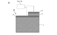
- FIG. 3 shows a schematic configuration diagram of a piezoelectric device 30 manufactured using the piezoelectric laminate 10 according to the present modification.
- the piezoelectric device 30 is configured to include at least a piezoelectric element 20 obtained by molding the piezoelectric laminated body 10 into a predetermined shape, and a voltage detection means 11a and a voltage application means 11b connected to the piezoelectric element 20. ..
- the piezoelectric element 20 has a pattern electrode formed by molding the electrode film 4 into a predetermined pattern.
- the piezoelectric element 20 has a pair of positive and negative pattern electrodes 4p 1 on the input side and a pair of positive and negative pattern electrodes 4p 2 on the output side.
- a comb-shaped electrode Inter Digital Transducer, abbreviated as IDT
- the piezoelectric device 30 is a filter such as a surface acoustic wave (abbreviation: SAW) filter. It can function as a device.
- SAW surface acoustic wave
- the frequency of the SAW to be excited can be adjusted, for example, by adjusting the pitch of the pattern electrode 4p 1 . For example, the shorter the IDT pitch as the pattern electrode 4p 1 , the higher the SAW frequency, and the longer the pitch, the lower the SAW frequency.
- the SAW having reached the pattern electrode 4p 2 propagates the KNN layer 3, SAW having a predetermined frequency (frequency component) which is determined according to the pitch or the like of the IDT as pattern electrode 4p 2 As a result, a voltage is generated between the pattern electrodes 4p 2 .
- the SAW having a predetermined frequency can be extracted from the excited SAW.
- the term "predetermined frequency” used herein may include not only the predetermined frequency but also a predetermined frequency band whose center frequency is the predetermined frequency.
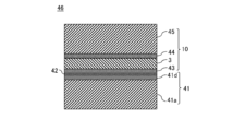
- the sacrificial layer 42 is formed on the first substrate 41, the first electrode film 43 is formed on the sacrificial layer 42, and the piezoelectric film ( The KNN film 3) is formed, the second electrode film 44 is formed on the KNN film 3, and the second substrate 45 is attached on the second electrode film 44 to form a laminated body 46.
- the KNN film 3 can be sufficiently oxidized to increase the light transmittance of the KNN film 3.
- the sacrificial layer 42 of the laminated body 46 is etched to form the laminated body 46 into the first substrate 41, the first electrode film 43, the KNN film 3, and the second electrode film 44. , And the piezoelectric laminated body 10 having the second substrate 45.
- the first substrate 41 is a substrate separated from the stacked body 46 as described later. Therefore, the first substrate 41 does not have to be a transparent substrate like the substrate 1 described above.
- the first substrate 41 as shown in FIG. 4A, single crystal silicon (Si) on which a surface oxide film (SiO 2 film) 41b such as a thermal oxide film or a CVD (Chemical Vapor Deposition) oxide film is formed.
- the substrate 41a that is, the Si substrate with the surface oxide film can be preferably used.
- the first substrate 41 as shown in FIG. 5, it is also possible to use a Si substrate 41a on the surface of which an insulating film 41d made of an insulating material other than SiO 2 is formed.
- the first substrate 41 it is also possible to use a Si substrate 41a having an exposed Si(100) face, Si(111) face, or the like, that is, a Si substrate having no surface oxide film 41b or insulating film 41d. it can.
- a Si substrate 41a As the first substrate 41, an SOI (Silicon On Insulator) substrate, a gallium arsenide (GaAs) substrate, or a metal substrate made of a metal material such as stainless steel can be used.
- the single crystal Si substrate 41a has a thickness of, for example, 300 to 1,000 ⁇ m
- the surface oxide film 41b has a thickness of, for example, 5 to 3,000 nm.
- the sacrificial layer 42 is formed using a material that disappears by etching described later.
- the sacrificial layer 42 can be formed using, for example, Ti, SRO, or zinc oxide (ZnO).
- the sacrificial layer 42 can be formed by a method such as a sputtering method or a vapor deposition method.
- the thickness of the sacrificial layer 42 can be set to, for example, 1 to 200 nm.
- Temperature eg substrate temperature: normal temperature (about 27°C) to 500°C, preferably 100 to 300°C Discharge power: 100-500W, preferably 200-400W
- Atmosphere Ar gas atmosphere Pressure of Ar gas atmosphere: 1 to 10 Pa, preferably 3 to 5 Pa Time: 3-8 minutes, preferably 3-6 minutes
- Temperature eg substrate temperature: 100-500°C, preferably 200-400°C
- Discharge power 1,000 to 1,500 W, preferably 1,200 to 1,300 W
- Atmosphere Ar gas atmosphere Pressure of Ar gas atmosphere: 0.1 to 0.5 Pa, preferably 0.2 to 0.4 Pa
- Processing time 30 seconds to 3 minutes, preferably 1 minute
- the first electrode film 43 is preferably composed of an electrode (transparent electrode) having a light transmittance of, for example, 65% or more in at least the visible light wavelength region, preferably in the visible light and near infrared wavelength regions.
- the first electrode film 43 is a film that is a base of the KNN film 3. Therefore, the first electrode film 43 preferably has the same crystal structure as the lower electrode film 2 in the above-described embodiment.
- the first electrode film 43 can be formed by using the same material, film forming method, conditions and the like as those of the lower electrode film 2 described above.
- the first electrode film 43 is a film serving as an upper electrode film in the piezoelectric element 20 (piezoelectric device 30) manufactured using the piezoelectric laminate 10.
- the second electrode film 44 is preferably composed of an electrode (transparent electrode) having a light transmittance of, for example, 65% or more in at least the visible light wavelength region, preferably the visible light and near-infrared wavelength regions.
- the second electrode film 44 does not greatly affect the crystal structure of the KNN film 3 unlike the first electrode film 43. Therefore, similarly to the upper electrode film 4 in the above-described embodiment, the crystal structure of the second electrode film 44 and the film forming method are not particularly limited.
- the second electrode film 44 can be formed by using the same material, film forming method, conditions and the like as those of the above-mentioned upper electrode film 4.
- the second electrode film 44 is a film serving as a lower electrode film in the piezoelectric element 20 (piezoelectric device 30) manufactured by using the piezoelectric laminate 10.
- the second substrate 45 it is preferable to use a substrate (transparent substrate) having a light transmittance of, for example, 65% or more at least in the visible light, preferably in the visible light and near-infrared wavelength region.
- the second substrate 45 like the second electrode film 44, does not significantly affect the crystal structure of the KNN film 3. Therefore, the material of the second substrate 45, the crystal structure, the surface (main surface) state such as the surface roughness, the forming method, the thickness, etc. are not particularly limited.
- the second substrate 45 preferably has flexibility in addition to light transmittance.
- a resin substrate (resin film) such as a polyimide substrate (polyimide film) can be preferably used.
- the bonding of the second substrate 45 onto the second electrode film 44 can be performed by adhesion, fusion, or the like.
- an adhesive containing an epoxy resin, a silicone resin or the like as a main component can be used.
- the above-mentioned adhesive is applied on the second electrode film 44 by a spin coating method or the like to form an adhesive layer, and the second substrate 45 is arranged on the adhesive layer, whereby The two substrates 45 can be bonded together.
- a metal such as gold (Au) or a heat-fusible material such as a heat-fusing film is used instead of the adhesive, and the second substrate 45 is placed on the above-mentioned material in a molten state. After the arrangement, the above materials can be solidified to carry out the bonding.
- the sacrifice layer 42 is etched by etching a solution containing either hydrogen chloride (HCl), diammonium cerium nitrate ((NH 4 ) 2 [Ce(NO 3 ) 6 ]), or acetic acid (CH 3 COOH). It can be performed by wet etching used as a liquid.
- the etching conditions such as the concentration of the etching solution, the etching time, and the etching temperature are adjusted depending on the material for forming the sacrificial layer 42, the thickness, the plane area, and the like.
- the stacked body 46 is immersed in a solution containing HCl at a concentration of 36.8%, for example, and the sacrificial layer 42 is etched. Further, for example, when the sacrificial layer 42 is formed using SRO, the laminated body 46 is immersed in a solution containing diammonium cerium nitrate at a concentration of, for example, 50 mol% to etch the sacrificial layer 42.
- the laminated body 46 is immersed in a solution containing acetic acid at a concentration of 33% and heated to 50 to 60° C., and the sacrificial layer 42 is etched.
- the present inventors have confirmed that, when the etching liquid is supplied to the laminated body 46 under the above-described conditions, only the etching of the sacrificial layer 42 of the laminated body 46 can be advanced. The sacrificial layer 42 disappears by etching.
- the second electrode film 44 may not be formed. That is, the second substrate 45 may be directly bonded onto the KNN film 3. Also in this case, the same bonding method and bonding conditions as described above can be used.
- the adhesion between the substrate 1 and the lower electrode film 2 or between the KNN film 3 and the upper electrode film 4 can be improved.
- Layers may be provided. The thickness of these adhesion layers can be, for example, 1 to 10 nm.
- the piezoelectric device 30 manufactured by using the piezoelectric laminated body 10 can be applied as long as it can be applied to a desired application such as a sensor or an actuator.
- the substrate 1 may be removed from the laminated body 10.
- the piezoelectric device 30 manufactured by processing the piezoelectric laminated body 10 is used for the application requiring the light transmittance as described above has been described, but the present invention is not limited to this.
- sensors such as an angular velocity sensor, an ultrasonic sensor, a pressure sensor, and an acceleration sensor, a head for an inkjet printer, a MEMS mirror for a scanner, an actuator such as a vibrator for an ultrasonic generator, and the like have optical transparency. It can also be used for applications that are not required to have.
- the substrate 1 does not have to be a transparent substrate.
- the substrate 1 for example, the same substrate as the first substrate 41 in the above modification may be used.
- the lower electrode film 2 (second electrode film 44) may not be formed of a transparent electrode.
- the lower electrode film 2 (second electrode film 44) can also be formed by using various metals such as Pt, Au, ruthenium (Ru), and iridium (Ir), and alloys containing these as the main components. In this case, the thickness of the lower electrode film 2 (second electrode film 44) can be set to 100 to 400 nm, for example.
- the upper electrode film 4 (first electrode film 43) does not have to be formed of a transparent electrode.
- the upper electrode film 4 (first electrode film 43) can be formed using, for example, various metals such as Pt, Au, aluminum (Al), and Cu, and alloys thereof.
- the thickness of the upper electrode film 4 (first electrode film 43) can be set to, for example, 100 to 5,000 nm.
- the adhesion layer may have a thickness of 1 to 200 nm, for example. Good.
- the second substrate 45 of the above-described modification may be a substrate formed of a metal material such as stainless steel or the like. Alternatively, a substrate formed of a plastic material or the like can be used. Further, as the second substrate 45, various substrates such as a Si substrate having a silicon nitride (SiN) film formed on its surface, a poly-Si substrate, or the like can be used. Further, as the second substrate 45, an SOI substrate or a SiO 2 substrate having a quality lower than that required for the substrate 1 or the first substrate 41 can be used. As an example of the low quality substrate, a substrate whose surface is rougher than that of the substrate 1 or the first substrate 41 (having a larger surface roughness than the substrate 1) can be given.
- a Si substrate (the surface is preferentially oriented in the (100) plane direction, thickness: 610 ⁇ m, diameter: 6 inches) was prepared.
- a thermal oxide film (thickness: 200 nm) is formed on the surface of the Si substrate.
- a Pt film as a lower electrode film preferential orientation in the (111) plane orientation with respect to the surface of the substrate, thickness: 200 nm
- a KNN film as a piezoelectric film (of the substrate)
- a preferential orientation in the (001) plane direction and a thickness of 2 ⁇ m were sequentially formed on the surface to form a piezoelectric laminate.
- the KNN film was heat-treated under predetermined conditions.
- the Pt film was formed by using the RF magnetron sputtering method.
- the conditions for forming the Pt film were as follows. Processing temperature: 300°C Discharge power: 1,200W Introduced gas: Ar gas Ar atmosphere pressure: 0.3 Pa Film formation time: 5 minutes
- the KNN film was formed by using the RF magnetron sputtering method.
- the conditions for forming the KNN film were as follows. Film forming temperature: 600°C Discharge power: 2,200W Introduced gas: Ar+O 2 mixed gas Ar+O 2 mixed gas atmosphere pressure: 0.3 Pa Partial pressure of Ar gas with respect to O 2 gas (Ar/O 2 partial pressure ratio): 25/1 Film formation speed: 1 ⁇ m/hr
- As the target material K 2 CO 3 powder, Na 2 CO 3 powder, Nb 2 O 5 powder, and CuO powder were mixed for 24 hours using a ball mill, and calcined at 850° C. for 10 hours, and then the ball mill was used again. It was produced by crushing with, and molding at a pressure of 200 MPa, and then firing at 1080°C.
- the composition of the target material is controlled by adjusting the mixing ratio of K 2 CO 3 powder, Na 2 CO 3 powder, Nb 2 O 5 powder, and CuO powder, and EDX (energy dispersive X Line spectroscopy).
- the heat treatment conditions applied to the KNN film were as follows. Heat treatment atmosphere: Air Heat treatment temperature: 650°C Heat treatment time: 48 hours
- the average light transmittance of the KNN film was evaluated by the following procedure. Using a spectroscopic ellipsometer, the light transmittance of the piezoelectric film (KNN film) of the piezoelectric laminate in the wavelength range of 380 to 1,400 nm was measured before and after the heat treatment. The light transmittance was measured every 1 nm in the wavelength range of 380 to 1,400 nm. Then, the average value (arithmetic average value) of the measured values of the light transmittance within the predetermined wavelength range was calculated, and the calculated value was defined as the average light transmittance. The calculation results of the average light transmittance are as shown in Table 1 below.
- the average light transmittance of the piezoelectric film in the visible light and near-infrared wavelength regions is higher after heat treatment than before heat treatment in any wavelength region. .. That is, it can be seen from Table 1 that the heat treatment can increase the light transmittance of the piezoelectric film in the visible and near-infrared wavelength regions. Further, it can be seen from Table 1 that even the KNN film containing Cu has an average light transmittance of 65% or more in the visible light and near infrared wavelength regions.
- (Appendix 1) According to one aspect of the invention, Board, An electrode film, A piezoelectric film made of an alkali niobium oxide having a perovskite structure represented by a composition formula (K 1-x Na x )NbO 3 (0 ⁇ x ⁇ 1), There is provided a piezoelectric laminate having an average light transmittance of 65% or more in the visible light and near-infrared wavelength regions of the piezoelectric film.
- Appendix 2 The piezoelectric laminate according to appendix 1, preferably The average light transmittance of the piezoelectric film in the visible light wavelength region is 56% or more.
- the piezoelectric laminate according to appendix 1 or 2 preferably, The piezoelectric film contains at least one metal element selected from the group consisting of Cu and Mn in a concentration of 0.2 at% or more and 2.0 at% or less.
- the electrode film has a light transmittance of 65% or more in at least a visible light wavelength region.
- Substrate, lower electrode film formed on the substrate, and perovskite film formed on the lower electrode film and represented by a composition formula (K 1-x Na x )NbO 3 (0 ⁇ x ⁇ 1) A piezoelectric film made of an alkali niobium oxide having a structure, and an upper electrode film formed on the piezoelectric film, and There is provided a piezoelectric element or a piezoelectric device having an average light transmittance of 65% or more in the visible light and near-infrared wavelength regions of the piezoelectric film.
- the piezoelectric element or the piezoelectric device of Supplementary Note 7 preferably, The light transmittance of at least the visible light wavelength region of the substrate, the lower electrode film, and the upper electrode film is 65% or more.
- Appendix 10 A piezoelectric element or a piezoelectric device according to Appendix 9, wherein The light transmittance of at least the visible light wavelength region of the substrate and the electrode film is 65% or more.
- the piezoelectric element or device according to any one of appendices 7 to 9 The piezoelectric element or device according to any one of appendices 7 to 9, The light transmittance of at least the visible light wavelength region of the entire piezoelectric laminate is 50% or more, preferably 60% or more.
- (A) A perovskite structure represented by a composition formula (K 1-x Na x )NbO 3 (0 ⁇ x ⁇ 1) on a substrate or on a substrate on which an electrode film is formed. And a step of forming a piezoelectric film made of alkali niobium oxide, In (a), by increasing the partial pressure of H 2 O in the film forming atmosphere of the piezoelectric film, the piezoelectric laminate in which the average light transmittance of the piezoelectric film in the wavelength region of visible light and near infrared light is 65% or more. A method of manufacturing the same is provided.
- (A) A perovskite structure represented by a composition formula (K 1-x Na x )NbO 3 (0 ⁇ x ⁇ 1) on a substrate or on a substrate on which an electrode film is formed.
- a step of forming a piezoelectric film made of alkali niobium oxide (B) performing a heat treatment on the piezoelectric film in the air or an oxygen-containing atmosphere, By carrying out (b) after carrying out (a), there is provided a method for manufacturing a piezoelectric laminate in which the piezoelectric film has an average light transmittance of 65% or more in the visible and near infrared wavelength regions.
Landscapes
- Chemical & Material Sciences (AREA)
- Engineering & Computer Science (AREA)
- Organic Chemistry (AREA)
- Manufacturing & Machinery (AREA)
- Materials Engineering (AREA)
- Physics & Mathematics (AREA)
- Ceramic Engineering (AREA)
- Acoustics & Sound (AREA)
- Inorganic Chemistry (AREA)
- Chemical Kinetics & Catalysis (AREA)
- Mechanical Engineering (AREA)
- Metallurgy (AREA)
- Thermal Sciences (AREA)
- Physical Vapour Deposition (AREA)
- Piezo-Electric Or Mechanical Vibrators, Or Delay Or Filter Circuits (AREA)
- Inorganic Compounds Of Heavy Metals (AREA)
Abstract
Description
基板と、
電極膜と、
組成式(K1-xNax)NbO3(0<x<1)で表されるペロブスカイト構造のアルカリニオブ酸化物からなる圧電膜と、を備え、
前記圧電膜の可視光および近赤外線の波長領域における平均光透過率が65%以上である圧電積層体およびその関連技術が提供される。
以下、本発明の一実施形態について図1~図2を参照しながら説明する。
図1に示すように、本実施形態にかかる圧電膜を有する積層体(積層基板)10(以下、圧電積層体10とも称する)は、基板1と、基板1上に製膜された下部電極膜2と、下部電極膜2上に製膜された圧電膜(圧電薄膜)3と、圧電膜3上に製膜された上部電極膜4と、を備えている。
図2に、本実施形態における圧電デバイス30の概略構成図を示す。圧電デバイス30は、上述の圧電積層体10を所定の形状に成形して得られる圧電素子20と、圧電素子20に接続される電圧検出手段11aまたは電圧印加手段11bと、を少なくとも備えて構成される。
続いて、上述の圧電積層体10の製造方法について説明する。まず、基板1のいずれかの主面上に下部電極膜2を製膜する。なお、いずれかの主面上に下部電極膜2が予め製膜された基板1を用意してもよい。続いて、下部電極膜2上に、例えばRFスパッタリング法を用いてKNN膜3を製膜する。その後、KNN膜3に対して熱処理を行う。そして、熱処理後のKNN膜3上に、例えばRFスパッタリング法を用いて上部電極膜4を製膜する。これにより、圧電積層体10が得られる。圧電積層体10をエッチング等により所定の形状に成形することで、圧電素子20が得られ、圧電素子20に電圧検出手段11aまたは電圧印加手段11bを接続することで、圧電デバイス30が得られる。
温度(製膜温度、例えば基板温度):常温(27℃程度)~500℃、好ましくは150~250℃、より好ましくは200℃程度
放電パワー:100~500W、好ましくは200~400W
導入ガス:Arガス
Arガス雰囲気の圧力:1~10Pa、好ましくは3~5Pa
製膜時間:3~10分、好ましくは5~6分
温度(製膜温度、例えば基板温度):100~500℃、好ましくは200~400℃
放電パワー:1,000~1,500W、好ましくは1,200~1300W
処理雰囲気:Arガス雰囲気
雰囲気圧力:0.1~0.5Pa、好ましくは0.2~0.4Pa
処理時間:30秒から2分、好ましくは1分程度
温度(製膜温度、例えば基板温度):500~700℃、好ましくは600℃
放電パワー:2,000~2,400W、好ましくは2,200W
導入ガス:Ar+O2混合ガス
Ar+O2混合ガス雰囲気の圧力:0.2~0.5Pa、好ましくは0.25~0.4Pa
O2ガスに対するArガスの分圧(Ar/O2分圧比):30/1~20/1、好ましくは27/1~23/1
製膜速度:0.5~2μm/hr、好ましくは1~1.5μm/hr
雰囲気:大気または酸素含有雰囲気
温度:600~1,000℃、好ましくは650~900℃、より好ましくは、上記範囲内の温度であってKNN膜の処理温度以上の温度
熱処理時間:KNN膜の厚さ1μmあたり0.5時間以上、好ましくは24時間以上、より好ましくは40時間以上
本実施形態によれば、以下に示す1つまたは複数の効果が得られる。
本実施形態は上述の態様に限定されず、以下のように変形することもできる。
圧電積層体10は、下部電極膜2を備えていなくてもよい。すなわち、圧電積層体10は、基板1と、基板1上に製膜されたKNN膜(圧電膜)3と、KNN膜3上に製膜された上部電極膜4(電極膜4)と、を備えて構成されていてもよい。
上述の実施形態では、基板1上に下部電極膜2、KNN膜3、および上部電極膜4を、この順に製膜して圧電積層体10を作製する場合について説明したが、これに限定されるものではない。圧電積層体10を以下のように作製してもよい。なお、本変形例では、上述の実施形態と同一の構成要素には、同一の符号を付し、その説明を省略する。
温度(例えば基板温度):常温(27℃程度)~500℃、好ましくは100~300℃
放電パワー:100~500W、好ましくは200~400W
雰囲気:Arガス雰囲気
Arガス雰囲気の圧力:1~10Pa、好ましくは3~5Pa
時間:3~8分、好ましくは3~6分
温度(例えば基板温度):100~500℃、好ましくは200~400℃
放電パワー:1,000~1,500W、好ましくは1,200~1,300W
雰囲気:Arガス雰囲気
Arガス雰囲気の圧力:0.1~0.5Pa、好ましくは0.2~0.4Pa
処理時間:30秒から3分、好ましくは1分
圧電積層体10全体の上述の光透過率を例えば50%以上に保つことができれば、基板1と下部電極膜2との間や、KNN膜3と上部電極膜4との間に、これらの密着性を高めるため、例えばチタン(Ti)、タンタル(Ta)、酸化チタン(TiO2)、ニッケル(Ni)、ルテニウム酸化物(RuOx)、イリジウム酸化物(IrOx)等を主成分とする密着層を設けてもよい。これらの密着層の厚さは例えば1~10nmとすることができる。
上述の圧電積層体10を圧電素子20に成形する際、圧電積層体10(圧電素子20)を用いて作製した圧電デバイス30をセンサやアクチュエータ等の所望の用途に適用することができる限り、圧電積層体10から基板1を除去してもよい。
以上、本発明の実施形態を具体的に説明した。但し、本発明は上述の実施形態に限定されるものではなく、その要旨を逸脱しない範囲で種々変更可能である。
処理温度:300℃
放電パワー:1,200W
導入ガス:Arガス
Ar雰囲気の圧力:0.3Pa
製膜時間:5分
製膜温度:600℃
放電パワー:2,200W
導入ガス:Ar+O2混合ガス
Ar+O2混合ガス雰囲気の圧力:0.3Pa
O2ガスに対するArガスの分圧(Ar/O2分圧比):25/1
製膜速度:1μm/hr
熱処理雰囲気:大気
熱処理温度:650℃
熱処理時間:48時間
KNN膜の平均光透過率の評価は、以下の手順で行った。分光エリプソメータを用い、熱処理を行う前と熱処理を行った後で、圧電積層体が有する圧電膜(KNN膜)の380~1,400nmの波長領域における光透過率を測定した。光透過率は、380~1,400nmの波長領域において1nm毎に測定した。そして、所定の波長範囲内における光透過率の測定値の平均値(算術平均値)を算出し、この算出した値を平均光透過率とした。平均光透過率の算出結果は下記の表1に示す通りである。

以下、本発明の好ましい態様について付記する。
本発明の一態様によれば、
基板と、
電極膜と、
組成式(K1-xNax)NbO3(0<x<1)で表されるペロブスカイト構造のアルカリニオブ酸化物がからなる圧電膜と、を備え、
前記圧電膜の可視光および近赤外線の波長領域における平均光透過率が65%以上である圧電積層体が提供される。
付記1の圧電積層体であって、好ましくは、
前記圧電膜の可視光の波長領域における平均光透過率が56%以上である。
付記1または2の圧電積層体であって、好ましくは、
前記圧電膜は、CuおよびMnからなる群より選択される少なくとも1つ以上の金属元素を、0.2at%以上2.0at%以下の濃度で含む。
付記1~3のいずれかの圧電積層体であって、好ましくは、
前記基板は、少なくとも可視光の波長領域における光透過率が65%以上である。
付記1~4のいずれかの圧電積層体であって、好ましくは、
前記電極膜は、少なくとも可視光の波長領域における光透過率が65%以上である。
付記1~5のいずれかの圧電積層体であって、好ましくは、
前記圧電積層体全体の少なくとも可視光の波長領域における光透過率が50%以上、好ましくは60%以上である。
本発明のさらに他の態様によれば、
基板と、前記基板上に製膜された下部電極膜と、前記下部電極膜上に製膜され、組成式(K1-xNax)NbO3(0<x<1)で表されるペロブスカイト構造のアルカリニオブ酸化物からなる圧電膜と、前記圧電膜上に製膜された上部電極膜と、を有する圧電積層体を備え、
前記圧電膜の可視光および近赤外線の波長領域における平均光透過率が65%以上である圧電素子または圧電デバイスが提供される。
付記7の圧電素子または圧電デバイスであって、好ましくは、
前記基板、前記下部電極膜、および前記上部電極膜の少なくとも可視光の波長領域における光透過率が65%以上である。
本発明のさらに他の態様によれば、
基板と、前記基板上に製膜され、組成式(K1-xNax)NbO3(0<x<1)で表されるペロブスカイト構造のアルカリニオブ酸化からなる圧電膜と、前記圧電膜上に製膜された電極膜と、を有する圧電積層体を備え、
前記圧電膜の可視光および近赤外線の波長領域における平均光透過率が65%以上である圧電素子または圧電デバイスが提供される。
付記9の圧電素子または圧電デバイスであって、
前記基板および前記電極膜の少なくとも可視光の波長領域における光透過率が65%以上である。
付記7~9のいずれかの圧電素子または圧電デバイスであって、
前記圧電積層体全体の少なくとも可視光の波長領域における光透過率が50%以上、好ましくは60%以上である。
本発明のさらに他の態様によれば、
(a)基板上、またはいずれかの主面上に電極膜が製膜された基板上に、組成式(K1-xNax)NbO3(0<x<1)で表されるペロブスカイト構造のアルカリニオブ酸化物からなる圧電膜を製膜する工程を有し、
(a)では、前記圧電膜の製膜雰囲気中のH2O分圧を高めることで、前記圧電膜の可視光および近赤外線の波長領域における平均光透過率を65%以上とする圧電積層体の製造方法が提供される。
本発明のさらに他の態様によれば、
(a)基板上、またはいずれかの主面上に電極膜が製膜された基板上に、組成式(K1-xNax)NbO3(0<x<1)で表されるペロブスカイト構造のアルカリニオブ酸化物からなる圧電膜を製膜する工程と、
(b)大気または酸素含有雰囲気で、前記圧電膜に対して熱処理を行う工程と、を有し、
(a)を行った後(b)を行うことで、前記圧電膜の可視光および近赤外線の波長領域における平均光透過率を65%以上とする圧電積層体の製造方法が提供される。
2 電極膜(下部電極膜)
3 圧電膜
4 電極膜(上部電極膜)
10 圧電積層体
Claims (8)
- 基板と、
電極膜と、
組成式(K1-xNax)NbO3(0<x<1)で表されるペロブスカイト構造のアルカリニオブ酸化物からなる圧電膜と、を備え、
前記圧電膜の可視光および近赤外線の波長領域における平均光透過率が65%以上である圧電積層体。 - 前記圧電膜の可視光の波長領域における平均光透過率が56%以上である請求項1に記載の圧電積層体。
- 前記基板は、少なくとも可視光の波長領域における光透過率が65%以上である請求項1または2に記載の圧電積層体。
- 前記電極膜は、少なくとも可視光の波長領域における光透過率が65%以上である請求項1~3のいずれか1項に記載の圧電積層体。
- 前記圧電積層体全体の少なくとも可視光の波長領域における光透過率が50%以上である請求項1~4のいずれか1項に記載の圧電積層体。
- 基板と、
電極膜と、
組成式(K1-xNax)NbO3(0<x<1)で表されるペロブスカイト構造のアルカリニオブ酸化からなる圧電膜と、を備え、
前記圧電膜の可視光および近赤外線の波長領域における平均光透過率が65%以上である圧電素子。 - (a)基板上、またはいずれかの主面上に電極膜が製膜された基板上に、組成式(K1-xNax)NbO3(0<x<1)で表されるペロブスカイト構造のアルカリニオブ酸化物からなる圧電膜を製膜する工程を有し、
(a)では、前記圧電膜の製膜雰囲気中のH2O分圧を高めることで、前記圧電膜の可視光および近赤外線の波長領域における平均光透過率を65%以上とする圧電積層体の製造方法。 - (a)基板上、またはいずれかの主面上に電極膜が製膜された基板上に、組成式(K1-xNax)NbO3(0<x<1)で表されるペロブスカイト構造のアルカリニオブ酸化物からなる圧電膜を製膜する工程と、
(b)大気または酸素含有雰囲気で、前記圧電膜に対して熱処理を行う工程と、を有し、
(a)を行った後(b)を行うことで、前記圧電膜の可視光および近赤外線の波長領域における平均光透過率を65%以上とする圧電積層体の製造方法。
Priority Applications (2)
| Application Number | Priority Date | Filing Date | Title |
|---|---|---|---|
| US17/299,951 US12408556B2 (en) | 2018-12-07 | 2019-11-14 | Piezoelectric stack, piezoelectric element, and method of manufacturing piezoelectric stack |
| EP19893646.0A EP3901097B1 (en) | 2018-12-07 | 2019-11-14 | Piezoelectric laminate, piezoelectric element, and piezoelectric laminate manufacturing method |
Applications Claiming Priority (2)
| Application Number | Priority Date | Filing Date | Title |
|---|---|---|---|
| JP2018-229831 | 2018-12-07 | ||
| JP2018229831A JP7352347B2 (ja) | 2018-12-07 | 2018-12-07 | 圧電積層体、圧電素子および圧電積層体の製造方法 |
Publications (1)
| Publication Number | Publication Date |
|---|---|
| WO2020116123A1 true WO2020116123A1 (ja) | 2020-06-11 |
Family
ID=70973987
Family Applications (1)
| Application Number | Title | Priority Date | Filing Date |
|---|---|---|---|
| PCT/JP2019/044775 Ceased WO2020116123A1 (ja) | 2018-12-07 | 2019-11-14 | 圧電積層体、圧電素子および圧電積層体の製造方法 |
Country Status (4)
| Country | Link |
|---|---|
| US (1) | US12408556B2 (ja) |
| EP (1) | EP3901097B1 (ja) |
| JP (1) | JP7352347B2 (ja) |
| WO (1) | WO2020116123A1 (ja) |
Cited By (2)
| Publication number | Priority date | Publication date | Assignee | Title |
|---|---|---|---|---|
| EP4318621A4 (en) * | 2021-03-30 | 2024-09-11 | FUJIFILM Corporation | Piezoelectric element and method for manufacturing piezoelectric element |
| TWI870582B (zh) * | 2020-06-30 | 2025-01-21 | 日商住友化學股份有限公司 | 壓電積層體、壓電元件及壓電積層體的製造方法 |
Families Citing this family (4)
| Publication number | Priority date | Publication date | Assignee | Title |
|---|---|---|---|---|
| EP3995454A4 (en) * | 2019-07-04 | 2023-08-09 | Sumitomo Chemical Company, Limited | PIEZOELECTRIC FILM, PIEZOELECTRIC LAMINATE BODY, PIEZOELECTRIC ELEMENT AND METHOD FOR MAKING PIEZOELECTRIC LAMINATE BODY |
| CN117084003A (zh) * | 2021-03-30 | 2023-11-17 | 富士胶片株式会社 | 压电元件及压电元件的制造方法 |
| KR102704454B1 (ko) * | 2021-11-30 | 2024-09-10 | 한국재료연구원 | 투명 knn 계열 페로브스카이트 시드 및 이의 제조방법 |
| TW202342632A (zh) * | 2022-04-21 | 2023-11-01 | 日商Dic股份有限公司 | 鉭酸鹽粒子、鉭酸鹽粒子的製造方法、樹脂組成物及成形體 |
Citations (6)
| Publication number | Priority date | Publication date | Assignee | Title |
|---|---|---|---|---|
| JP2007184513A (ja) | 2005-12-06 | 2007-07-19 | Seiko Epson Corp | 圧電体積層体、表面弾性波素子、薄膜圧電共振子および圧電アクチュエータ |
| JP2008159807A (ja) | 2006-12-22 | 2008-07-10 | Hitachi Cable Ltd | 圧電薄膜素子及び圧電薄膜素子を用いて製造したアクチュエータとセンサ |
| JP2011143259A (ja) * | 2011-02-28 | 2011-07-28 | Toshiba Corp | 生体情報計測装置 |
| US20150376068A1 (en) * | 2013-02-06 | 2015-12-31 | Agency for Science, Tecnology and Research | Electro-optic ceramic materials |
| JP2017538189A (ja) * | 2014-10-14 | 2017-12-21 | コーニング インコーポレイテッド | 圧電フィルム構造体およびセンサ並びにそれらを用いた表示アセンブリ |
| JP2018190891A (ja) * | 2017-05-10 | 2018-11-29 | 株式会社サイオクス | 圧電膜を有する積層基板の製造方法、圧電膜を有する素子の製造方法および圧電膜を有する積層体 |
Family Cites Families (9)
| Publication number | Priority date | Publication date | Assignee | Title |
|---|---|---|---|---|
| JP2011179021A (ja) | 2010-02-26 | 2011-09-15 | Tohoku Univ | 導電体および導電体の製造方法 |
| JP5071503B2 (ja) * | 2010-03-25 | 2012-11-14 | 日立電線株式会社 | 圧電薄膜素子及び圧電薄膜デバイス |
| JP5056914B2 (ja) * | 2010-07-07 | 2012-10-24 | 日立電線株式会社 | 圧電薄膜素子および圧電薄膜デバイス |
| JP2013197553A (ja) | 2012-03-22 | 2013-09-30 | Hitachi Cable Ltd | 圧電体膜付き基板、圧電体膜素子及びその製造方法 |
| JP6239566B2 (ja) * | 2015-10-16 | 2017-11-29 | 株式会社サイオクス | 圧電薄膜付き積層基板、圧電薄膜素子およびその製造方法 |
| CN105819856B (zh) | 2016-03-14 | 2018-03-06 | 陕西师范大学 | 铌酸钾钠基无铅透明铁电陶瓷材料及其制备方法 |
| WO2018064722A1 (en) * | 2016-10-05 | 2018-04-12 | Newsouth Innovations Pty Limited | Piezoelectric contact sensor |
| JP2019021994A (ja) * | 2017-07-12 | 2019-02-07 | 株式会社サイオクス | 圧電膜を有する積層基板、圧電膜を有する素子および圧電膜を有する積層基板の製造方法 |
| JP6502460B2 (ja) | 2017-11-01 | 2019-04-17 | 株式会社サイオクス | 圧電薄膜付き積層基板および圧電薄膜素子 |
-
2018
- 2018-12-07 JP JP2018229831A patent/JP7352347B2/ja active Active
-
2019
- 2019-11-14 WO PCT/JP2019/044775 patent/WO2020116123A1/ja not_active Ceased
- 2019-11-14 EP EP19893646.0A patent/EP3901097B1/en active Active
- 2019-11-14 US US17/299,951 patent/US12408556B2/en active Active
Patent Citations (6)
| Publication number | Priority date | Publication date | Assignee | Title |
|---|---|---|---|---|
| JP2007184513A (ja) | 2005-12-06 | 2007-07-19 | Seiko Epson Corp | 圧電体積層体、表面弾性波素子、薄膜圧電共振子および圧電アクチュエータ |
| JP2008159807A (ja) | 2006-12-22 | 2008-07-10 | Hitachi Cable Ltd | 圧電薄膜素子及び圧電薄膜素子を用いて製造したアクチュエータとセンサ |
| JP2011143259A (ja) * | 2011-02-28 | 2011-07-28 | Toshiba Corp | 生体情報計測装置 |
| US20150376068A1 (en) * | 2013-02-06 | 2015-12-31 | Agency for Science, Tecnology and Research | Electro-optic ceramic materials |
| JP2017538189A (ja) * | 2014-10-14 | 2017-12-21 | コーニング インコーポレイテッド | 圧電フィルム構造体およびセンサ並びにそれらを用いた表示アセンブリ |
| JP2018190891A (ja) * | 2017-05-10 | 2018-11-29 | 株式会社サイオクス | 圧電膜を有する積層基板の製造方法、圧電膜を有する素子の製造方法および圧電膜を有する積層体 |
Cited By (2)
| Publication number | Priority date | Publication date | Assignee | Title |
|---|---|---|---|---|
| TWI870582B (zh) * | 2020-06-30 | 2025-01-21 | 日商住友化學股份有限公司 | 壓電積層體、壓電元件及壓電積層體的製造方法 |
| EP4318621A4 (en) * | 2021-03-30 | 2024-09-11 | FUJIFILM Corporation | Piezoelectric element and method for manufacturing piezoelectric element |
Also Published As
| Publication number | Publication date |
|---|---|
| EP3901097B1 (en) | 2025-08-06 |
| JP7352347B2 (ja) | 2023-09-28 |
| US12408556B2 (en) | 2025-09-02 |
| EP3901097C0 (en) | 2025-08-06 |
| US20230135208A1 (en) | 2023-05-04 |
| JP2020092228A (ja) | 2020-06-11 |
| EP3901097A1 (en) | 2021-10-27 |
| EP3901097A4 (en) | 2023-06-28 |
Similar Documents
| Publication | Publication Date | Title |
|---|---|---|
| JP7352347B2 (ja) | 圧電積層体、圧電素子および圧電積層体の製造方法 | |
| JP6239566B2 (ja) | 圧電薄膜付き積層基板、圧電薄膜素子およびその製造方法 | |
| US8446074B2 (en) | Piezoelectric thin-film element and piezoelectric thin-film device | |
| CN102959751B (zh) | 压电膜器件和压电膜装置 | |
| JP7074512B2 (ja) | 圧電積層体、圧電積層体の製造方法、圧電素子、およびスパッタリングターゲット材 | |
| JP6342040B1 (ja) | 圧電膜を有する積層基板、圧電膜を有する素子および圧電膜を有する積層基板の製造方法 | |
| JP2014187094A (ja) | 圧電体薄膜積層基板、圧電体薄膜素子、およびそれらの製造方法 | |
| JP7044600B2 (ja) | 圧電積層体、圧電積層体の製造方法および圧電デバイス | |
| TW202505987A (zh) | 壓電積層體、壓電積層體的製造方法、及壓電元件 | |
| US20200161533A1 (en) | Laminated substrate having piezoelectric film, element having piezoelectric film and method for manufacturing this laminated substrate | |
| JP7696347B2 (ja) | 圧電積層体、圧電素子および圧電積層体の製造方法 | |
| JP6934746B2 (ja) | 圧電膜を有する積層基板、圧電膜を有する素子および圧電膜を有する積層基板の製造方法 | |
| JP7022853B2 (ja) | スパッタリングターゲット材、スパッタリングターゲット材の製造方法、および圧電薄膜付き積層基板の製造方法 | |
| JP7037892B2 (ja) | 圧電膜を有する積層基板の製造方法、圧電膜を有する素子の製造方法および圧電膜を有する積層体 | |
| JP6964511B2 (ja) | 圧電積層体、圧電積層体の製造方法および圧電素子 | |
| JP7464360B2 (ja) | 圧電積層体、圧電素子および圧電積層体の製造方法 | |
| JP6502460B2 (ja) | 圧電薄膜付き積層基板および圧電薄膜素子 | |
| JP6758444B2 (ja) | 圧電薄膜付き積層基板および圧電薄膜素子 | |
| JP6607993B2 (ja) | 圧電膜を有する積層基板、圧電膜を有する素子および圧電膜を有する積層基板の製造方法 | |
| TW202137590A (zh) | 壓電膜、壓電積層體、壓電元件及壓電積層體的製造方法 | |
| JP7320098B2 (ja) | 圧電積層体、圧電積層体の製造方法および圧電デバイス | |
| JP6961770B2 (ja) | 圧電薄膜付き積層基板および圧電薄膜素子 | |
| JP7320091B2 (ja) | 圧電薄膜付き積層基板、圧電薄膜付き積層基板の製造方法、圧電薄膜素子、スパッタリングターゲット材、およびスパッタリングターゲット材の製造方法 | |
| JP6804615B2 (ja) | 圧電膜を有する積層基板、圧電膜を有する素子および圧電膜を有する積層基板の製造方法 | |
| TW202439963A (zh) | 壓電積層體、壓電積層體的製造方法、及壓電元件 |
Legal Events
| Date | Code | Title | Description |
|---|---|---|---|
| 121 | Ep: the epo has been informed by wipo that ep was designated in this application |
Ref document number: 19893646 Country of ref document: EP Kind code of ref document: A1 |
|
| NENP | Non-entry into the national phase |
Ref country code: DE |
|
| ENP | Entry into the national phase |
Ref document number: 2019893646 Country of ref document: EP Effective date: 20210707 |
|
| WWG | Wipo information: grant in national office |
Ref document number: 2019893646 Country of ref document: EP |
|
| WWG | Wipo information: grant in national office |
Ref document number: 17299951 Country of ref document: US |