WO2020121600A1 - 部分放電検出装置及び部分放電検出方法 - Google Patents
部分放電検出装置及び部分放電検出方法 Download PDFInfo
- Publication number
- WO2020121600A1 WO2020121600A1 PCT/JP2019/032828 JP2019032828W WO2020121600A1 WO 2020121600 A1 WO2020121600 A1 WO 2020121600A1 JP 2019032828 W JP2019032828 W JP 2019032828W WO 2020121600 A1 WO2020121600 A1 WO 2020121600A1
- Authority
- WO
- WIPO (PCT)
- Prior art keywords
- partial discharge
- digital signal
- converter
- waveform
- data
- Prior art date
- Legal status (The legal status is an assumption and is not a legal conclusion. Google has not performed a legal analysis and makes no representation as to the accuracy of the status listed.)
- Ceased
Links
Images


Classifications
-
- G—PHYSICS
- G01—MEASURING; TESTING
- G01R—MEASURING ELECTRIC VARIABLES; MEASURING MAGNETIC VARIABLES
- G01R31/00—Arrangements for testing electric properties; Arrangements for locating electric faults; Arrangements for electrical testing characterised by what is being tested not provided for elsewhere
- G01R31/12—Testing dielectric strength or breakdown voltage ; Testing or monitoring effectiveness or level of insulation, e.g. of a cable or of an apparatus, for example using partial discharge measurements; Electrostatic testing
- G01R31/1227—Testing dielectric strength or breakdown voltage ; Testing or monitoring effectiveness or level of insulation, e.g. of a cable or of an apparatus, for example using partial discharge measurements; Electrostatic testing of components, parts or materials
- G01R31/1263—Testing dielectric strength or breakdown voltage ; Testing or monitoring effectiveness or level of insulation, e.g. of a cable or of an apparatus, for example using partial discharge measurements; Electrostatic testing of components, parts or materials of solid or fluid materials, e.g. insulation films, bulk material; of semiconductors or LV electronic components or parts; of cable, line or wire insulation
- G01R31/1272—Testing dielectric strength or breakdown voltage ; Testing or monitoring effectiveness or level of insulation, e.g. of a cable or of an apparatus, for example using partial discharge measurements; Electrostatic testing of components, parts or materials of solid or fluid materials, e.g. insulation films, bulk material; of semiconductors or LV electronic components or parts; of cable, line or wire insulation of cable, line or wire insulation, e.g. using partial discharge measurements
-
- G—PHYSICS
- G01—MEASURING; TESTING
- G01R—MEASURING ELECTRIC VARIABLES; MEASURING MAGNETIC VARIABLES
- G01R19/00—Arrangements for measuring currents or voltages or for indicating presence or sign thereof
- G01R19/25—Arrangements for measuring currents or voltages or for indicating presence or sign thereof using digital measurement techniques
- G01R19/2506—Arrangements for conditioning or analysing measured signals, e.g. for indicating peak values ; Details concerning sampling, digitizing or waveform capturing
- G01R19/2509—Details concerning sampling, digitizing or waveform capturing
-
- G—PHYSICS
- G01—MEASURING; TESTING
- G01R—MEASURING ELECTRIC VARIABLES; MEASURING MAGNETIC VARIABLES
- G01R31/00—Arrangements for testing electric properties; Arrangements for locating electric faults; Arrangements for electrical testing characterised by what is being tested not provided for elsewhere
- G01R31/12—Testing dielectric strength or breakdown voltage ; Testing or monitoring effectiveness or level of insulation, e.g. of a cable or of an apparatus, for example using partial discharge measurements; Electrostatic testing
- G01R31/14—Circuits therefor, e.g. for generating test voltages, sensing circuits
-
- G—PHYSICS
- G01—MEASURING; TESTING
- G01R—MEASURING ELECTRIC VARIABLES; MEASURING MAGNETIC VARIABLES
- G01R31/00—Arrangements for testing electric properties; Arrangements for locating electric faults; Arrangements for electrical testing characterised by what is being tested not provided for elsewhere
- G01R31/50—Testing of electric apparatus, lines, cables or components for short-circuits, continuity, leakage current or incorrect line connections
- G01R31/52—Testing for short-circuits, leakage current or ground faults
Definitions
- the present invention relates to a partial discharge detection device and a partial discharge detection method.
- CT current measuring device
- Patent Document 1 discloses a technique for observing a sign of insulation deterioration of a cable by measuring a charge amount of partial discharge generated when a high voltage is applied to a cable insulator.
- the partial discharge discharge pulse measured by the current measuring device is an analog signal, it is necessary to digitize the analog signal with the AD converter. Partial discharge is observed as an analog waveform of a high-frequency pulse generated at minute intervals, so it is necessary to measure the discharge pulse of the partial discharge in a wide frequency band. Further, the AD converter needs to operate so as to satisfy the sampling theorem.
- ultra-high-speed sampling is required for the AD converter to digitize and measure analog signals in a wide range of frequency bands under the conditions that satisfy the sampling theorem.
- An AD converter capable of ultra-high-speed sampling is extremely expensive, and AD-converted digital data is also output at ultra-high speed.
- signal processing of digital data is also required to be extremely fast.
- a high-speed and expensive FPGA Field Programmable Gate Array
- executes signal processing is used in order to support signal processing performed at ultra-high speed. Therefore, the hardware for measuring the partial discharge pulse becomes expensive.
- the inventor has studied to adopt an AD converter that does not operate at ultra-high speed under the condition that the sampling theorem is not satisfied.
- the analog signal is AD-converted under the condition that the sampling theorem is not satisfied, the partial discharge pulse is observed as aliasing noise in the entire Nyquist frequency band of the first, second, third,..., Nth Nyquist. If it suffices only to check the presence or absence of the partial discharge pulse, there is no problem even if the aliasing noise is observed.
- the SN ratio (Signal-to-Noise ratio) in the frequency band of the 1st, 2nd, 3rd,..., Nth Nyquist boundary becomes significantly worse. If the frequency band of the partial discharge pulse was at the boundary of Nyquist, the SN ratio would be poor, and the partial discharge pulse could not be observed.
- the present invention has been made in view of such a situation, and an object thereof is to make it possible to detect a partial discharge pulse under a condition that does not satisfy the sampling theorem even in a wide band.
- the present invention is a partial discharge detection device for detecting a partial discharge in a power cable to grasp the insulation deterioration state of the power cable.
- the partial discharge detection device includes a first converter that converts an analog signal of an AC waveform flowing in a power cable into a digital signal, and a partial discharge of a partial discharge in a plurality of Nyquist frequency regions defined for two different sampling frequencies.
- a signal processing unit that detects the occurrence of partial discharge based on the maximum value or sum of current values obtained from the digital signal of the partial discharge current converted in.
- FIG. 3 is an enlarged view of one segment and segmentation of a specific phase interval of an AC waveform of a measured current used for processing partial discharge data according to the first embodiment of the present invention.
- 4 is a flowchart of a method of processing partial discharge data according to the first embodiment of the present invention. It is a block diagram which shows the detailed structural example of the digital signal processing part of the partial discharge detection of the partial discharge detection apparatus which concerns on the 1st Embodiment of this invention.
- FIG. 6 is a flowchart showing an example of a process of clearing the partial discharge information table and transmitting partial discharge information to a communication unit according to the first embodiment of the present invention. It is explanatory drawing which shows the example of the timing which clears the partial discharge information table which concerns on the 1st Embodiment of this invention, and the timing which partial discharge information is transmitted. It is a flowchart which shows the example of the process which the high-order measuring apparatus which concerns on the 1st Embodiment of this invention determines the presence or absence of insulation deterioration of a power cable. It is a block diagram which shows the schematic structural example of the partial discharge detection system 1 comprised using the partial discharge detection apparatus which concerns on the 2nd Embodiment of this invention.
- FIG. 1 is a block diagram showing a schematic configuration example of a partial discharge detection system 1 configured by using the partial discharge detection device 1000 according to the first embodiment.
- the intermediate junction box 10 is provided so as to connect the power cables 30 to each other, and is grounded by a ground wire.
- a current measuring device (for example, high frequency CT) 40 for measuring partial discharge is attached to the ground wire.
- the Rogowski coil 20 for measuring an AC waveform is attached to the power cable 30.
- the partial discharge detection device 1000 is connected to the current measuring device 40 and the Rogowski coil 20, respectively. Then, the partial discharge detection device 1000 can detect the partial discharge in the power cable 30 and grasp the insulation deterioration state of the power cable 30 by using the partial discharge detection method according to the present embodiment.
- the partial discharge detection device 1000 is configured to exchange data with the host measurement device 60 via the external network 50. As described above, the Rogowski coil 20, the current measuring device 40, and the partial discharge detection device 1000 are provided for the power cable 30 and the intermediate junction box 10, and the partial discharge detection device 1000 and the upper measurement device 60 exchange data.
- the partial discharge detection system 1 is configured to do so.
- the analog signals (analog values) output from the current measuring device 40 and the Rogowski coil 20 are input to the partial discharge detection device 1000.
- the signal output from the current measuring device 40 is a current signal flowing through the ground line during partial discharge.
- the partial discharge detection device 1000 includes a low frequency analog input circuit 1100, a low speed AD converter 1110, a high frequency analog input circuit 1200, a high speed AD converter 1210, a partial discharge detection digital signal processing unit 1300, and a communication unit 1400.
- the low-frequency analog input circuit 1100 is supplied with the analog signal of the AC waveform of the commercial frequency output from the Rogowski coil 20.
- the partial discharge detection digital signal processing unit 1300 acquires voltage phase information from this signal.
- the low-speed AD converter 1110 corresponds to a first converter that converts an AC waveform analog signal flowing through the power cable 30 into a digital signal, and is an AC waveform analog input to the low-frequency analog input circuit 1100. Digitize the signal.
- the AC waveform digital signal digitized by the low-speed AD converter 1110 is input to the partial discharge detection digital signal processing unit 1300.
- the analog signal of the partial discharge current output from the current measuring device 40 is input to the high frequency analog input circuit 1200.
- the high-speed AD converter 1210 corresponds to a second converter that converts an analog signal of a partial discharge current into a digital signal in a plurality of Nyquist frequency regions defined for each of two different sampling frequencies. .. Therefore, the high-speed AD converter 1210 digitizes the analog signal of the partial discharge current input from the high-frequency analog input circuit 1200.
- the partial discharge digital signal digitized by the high-speed AD converter 1210 is input to the partial discharge detection digital signal processing unit 1300.
- the sampling frequency switch 1220 switches the sampling mode of the high-speed AD converter 1210 based on the switching signal input from the digital signal processing unit 1300 for detecting partial discharge.
- the sampling mode includes, for example, a 180 MHz mode and a 200 MHz mode. Then, the sampling frequency switch 1220 outputs a sampling clock of either 180 MHz or 200 MHz to the high-speed AD converter 1210 according to the sampling mode signal.
- the high-speed AD converter 1210 switches the sampling frequency for each cycle of the AC waveform according to the sampling clock input from the sampling frequency switch 1220, and samples the analog signal of the partial discharge current at 180 MHz or 200 MHz to digitize it. ..
- the high-speed AD converter 1210 uses the first sampling frequency (180 MHz) and the second sampling frequency (200 MHz) as the two different sampling frequencies.
- the value of the least common multiple (900 MHz) of the half value (90 MHz) of the first sampling frequency and the half value (100 MHz) of the second sampling frequency. Is larger than the frequency band of partial discharge (for example, 50 MHz to 800 MHz).
- the digital signal processing unit 1300 for detecting partial discharge includes a portion converted by the high-speed AD converter 1210 for each phase of the AC waveform obtained from the digital signal of the AC waveform flowing through the power cable 30 converted by the low-speed AD converter 1110. Occurrence of partial discharge is detected based on the maximum value or sum of current values obtained from the digital signal of discharge current. Therefore, the partial discharge detection digital signal processing unit 1300 obtains the phase of the AC waveform from the AC waveform digital signal digitized by the low-speed AD converter 1110. Then, the phase information of the obtained AC waveform is used to process the digital signal of the partial discharge current digitized in the high-speed AD converter 1210.
- the communication unit 1400 outputs the data (detection result of partial discharge) recorded in the partial discharge information table 1305 shown in FIG. 4 to the upper measurement device 60 connected to the external network 50 and monitoring partial discharge.
- the data output to the upper-level measuring device 60 is all the data recorded in the partial discharge information table 1305, but may be only a part of the data.
- a plurality of partial discharge detection devices 1000 are provided for the whole of a large number of power cables 30 connected by the intermediate junction box 10.
- the upper-level measuring device 60 comprehensively monitors the detection results of the plurality of partial discharge detecting devices 1000 via the external network 50, and determines a sign of insulation deterioration of the power cable 30.
- the partial discharge detection device 1000 uses both the baseband sampling method and the undersampling method to perform analog/digital conversion in the high-speed AD converter 1210.
- the baseband sampling method the first Nyquist frequency band 0 to 1/2 ⁇ Fs (sampling frequency) is an analog input band that can be digitized.
- the under-sampling method corresponds to an analog input in a frequency band higher than the sampling frequency, and includes the second, third,... Nth Nyquist frequency bands (n-1)/2 to n/2. This is a sampling method limited to a specific Nyquist frequency band such as Fs. Then, by using the baseband sampling method and the undersampling method together, the high frequency analog input circuit 1200 can input a wideband analog signal to the high speed AD converter 1210.
- FIG. 2 is an enlarged view showing an example of one section and division into specific phase intervals of the AC waveform of the measured current used for processing the partial discharge data.
- the horizontal axis represents the phase and the vertical axis represents the voltage.
- the partial discharge detection digital signal processing unit 1300 obtains the charge amount in that section of the partial discharge from the digitized signal. As the charge amount, the sum of the partial discharge pulse signals 1320 or the maximum value 1330 of the partial discharge pulse signals 1320 is obtained. Similarly, the partial discharge detection digital signal processing unit 1300 obtains the sum or maximum value 1330 of the partial discharge pulse signals 1320 as the charge amount of each section in all sections of a specific phase interval.
- the specific phase interval is calculated by dividing one cycle 360° of the AC waveform of 50 Hz or 60 Hz by a predetermined number. For example, by dividing one cycle of 360° into 96 sections, one section can have a phase interval of 3.75°. Note that, in FIG. 2, for convenience of illustration, one cycle of the AC waveform is divided into 20 sections for convenience, but it is not limited to 20 sections in FIG. 2.
- an AC waveform digital signal digitized from the AC waveform analog signal in the low-speed AD converter 1110 is used. Then, the phase of the AC waveform is obtained from the digital signal of the AC waveform, and the obtained phase of the AC waveform is used to divide into specific phase intervals as shown in FIG.
- the digital signal processing unit 1300 for detecting partial discharge obtains the sum or maximum value of the partial discharge pulse signals 1320 as the charge amount of partial discharge in all sections of a specific phase interval. Then, by the signal processing in the digital signal processing unit 1300 for detecting partial discharge, the data of the obtained charge amount of partial discharge is thinned out.
- the charge amount of partial discharge (the total sum or the maximum value of the amplitudes of the partial discharge pulse signals 1320) in all the intervals of a specific phase interval in a predetermined cycle of the AC waveform. ), only the maximum charge amount is extracted and recorded. As a result, the digital data of the predetermined number of cycles in the entire interval of the phase interval is thinned out into one data representing the maximum charge amount.
- the predetermined cycle of the AC waveform is selected from the range of 5 to 20 cycles, for example.
- the maximum value charge amount after thinning changes depending on the presence or absence of partial discharge.
- the presence or absence of partial discharge is reflected in the maximum charge amount. Therefore, the presence or absence of partial discharge can be detected by the maximum charge amount.
- the partial discharge detection digital signal processing unit 1300 thins out the data, and the remaining data (the extracted maximum amount of charge amount data) is transferred from the communication unit 1400 via the external network 50 to the higher-level measuring device 60. Send to.
- the upper-level measuring device 60 monitors the transition of the data (the maximum charge amount data) received from the external network 50. By monitoring the transition of the maximum charge amount in the upper measurement device 60, it is possible to monitor the sign of the insulation deterioration of the power cable 30. In addition, the life of the existing power cable 30 can be predicted by checking the deterioration state of the power cable 30. Then, in the upper measuring device 60, if the comparison of the current maximum charge amount data of the partial discharge received and the maximum charge amount data of the partial discharge received in the past is continuously performed, It is possible to grasp the progress status of deterioration of the large number of power cables 30 at any time.
- FIG. 3 is a flowchart showing an example of a method of processing partial discharge data.
- the partial discharge detection digital signal processing unit 1300 obtains the maximum value or the sum of the currents in each section of the AC waveform at a specific phase interval in all sections, and sets this as the charge amount in each section (S1). ..
- the partial discharge detection digital signal processing unit 1300 extracts the maximum value of the charge amount in the section for each predetermined number of cycles of the AC waveform (S2). As a result, (the number of sections in one cycle ⁇ the number of cycles) pieces of data are thinned out to one piece of data.
- the partial discharge detection digital signal processing unit 1300 transmits the extracted maximum value data of the charge amount to the host measuring device 60 via the communication unit 1400 (S3). In this way, the data thinned out by the extraction is transmitted to the upper measuring apparatus 60, so that the amount of data to be transmitted to the upper measuring apparatus 60 can be reduced.
- the partial discharge detection device 1000 is always installed in the power cable 30, and monitors the state of the power cable 30. Then, the partial discharge detection apparatus 1000 can reduce the cost and power consumption of the digital signal processing unit 1300 for partial discharge detection by thinning out the data and reducing the amount of data to be sent to the upper measurement apparatus 60. As a result, it is possible to always install the partial discharge detection device 1000.
- the low-frequency analog input circuit 1100, the high-frequency analog input circuit 1200, the low-speed AD converter 1110, the high-speed AD converter 1210, and the partial discharge detection digital signal processing unit 1300 shown in FIG. 1 are either hardware or computer software. But it can be configured. When each processing unit is configured by hardware, it is configured by an integrated circuit or the like provided in the partial discharge detection device 1000. When each processing unit is configured by computer software, a processor such as a microcomputer can interpret and execute a program that realizes each function of an analog input circuit, an AD converter, and a digital signal processing unit for partial discharge detection. It is configured so that It is also possible to configure part of the hardware and the rest of the computer software.
- the low frequency analog input circuit 1100, the high frequency analog input circuit 1200, the low speed AD converter 1110, the high speed AD converter 1210, and the partial discharge detection digital signal processing unit 1300 shown in FIG. 1 are configured by hardware.
- these processing units are configured by computer software, a memory for storing calculation results and the like is required, and power for activating the software and operating the memory is also required.
- power for starting the software and the operation of the memory is not required, so that the operation of the partial discharge detection apparatus 1000 can be performed as compared with the case of being configured by computer software. The required power can be reduced. As a result, it is possible to install a larger number of partial discharge detection devices 1000 for the entire number of power cables 30.
- the folding noise filter of the high frequency analog input circuit 1200 it is possible to pass analog signals in a plurality of Nyquist frequency regions as shown in FIG. 6 described later. Then, in the high-speed AD converter 1210, the analog signals in the plurality of Nyquist frequency regions are converted into digital signals. As a result, an analog signal in a wide band (for example, 50 MHz to 800 MHz) of a plurality of Nyquist frequency regions is converted into a digital signal, so that partial discharge that occurs over a wide band can be detected.
- a wide band for example, 50 MHz to 800 MHz
- the sampling frequency can be reduced compared to the baseband sampling method that converts the analog signal in the first Nyquist frequency domain. Accordingly, it is not necessary to use expensive components for the high-speed AD converter 1210 and the digital signal processing unit 1300, and the high-speed AD converter 1210 and the digital signal processing unit 1300 can be configured with relatively inexpensive components. Therefore, it is possible to realize a configuration for detecting partial discharge by combining relatively inexpensive parts.
- the partial discharge detection digital signal processing unit 1300 divides one cycle of the AC waveform into a predetermined phase interval, and the charge amount of the partial discharge (the maximum value of the partial discharge current value is Value or sum). As a result, the whole signal of the partial discharge current digital signal digitally converted by the high-speed AD converter 1210 becomes a signal of the partial discharge charge amount (maximum value or sum of currents), so that the amount of the signal is reduced. It
- the partial discharge detection digital signal processing unit 1300 extracts the maximum value of the partial discharge charge amount in each predetermined number of cycles of the AC waveform in the entire section. As a result, the signals of the charge amount of (the number of sections ⁇ the predetermined number of cycles) are thinned out to one signal of the maximum charge amount, and the amount of the signal is reduced.
- the partial discharge detection digital signal processing unit 1300 performs processing for reducing the amount of the partial discharge current signal that has been digitally converted by the high-speed AD converter 1210. This reduces the amount of processed signals even when handling signals in a wide range of Nyquist frequency regions. Since the amount of signals is reduced, the configuration (memory or the like) for storing signals is simplified, overflow is prevented when data is transmitted from the communication unit 1400 to the external network 50, and the power consumption of the partial discharge detection device 1000 is reduced. It becomes possible to realize reductions and the like.
- the phase of the AC waveform is obtained from the digital signal of the AC waveform that has been digitally converted by the low-speed AD converter 1110, and the phase of the AC waveform is used to divide into sections of a predetermined phase interval to reduce the partial discharge signal. It is carried out.
- the phase of the AC waveform By using the phase of the AC waveform, the amount of the signal can be easily reduced from the signal in the wide frequency range.
- the power consumption of the partial discharge detection device 1000 can be reduced, it is possible to install a larger number of partial discharge detection devices 1000 for the entire number of power cables 30. Further, in contrast to the conventional detection method, which was mainly to move the partial discharge detection device to a position to be measured, a large number of partial discharge detection devices 1000 were installed stationary, and the partial discharge detection device 60 It becomes possible to constantly monitor the occurrence.
- the first embodiment from the entire signal of the digital signal of the partial discharge current digitally converted by the high-speed AD converter 1210, one of the maximum charge amounts is obtained for each predetermined number of cycles of the AC waveform. Since it is reduced to a signal, the amount of signal is greatly reduced. As a result, the effect of simplifying the configuration (memory or the like) for storing signals and reducing the power consumption of the partial discharge detection apparatus 1000 is increased, and the configuration of the partial discharge detection apparatus 1000 is simplified and the cost of parts is reduced. Can be achieved.
- the partial discharge detection device 1000 is provided with a communication unit 1400, the communication unit 1400 is connected to the host measurement device 60 via the external network 50, and the communication unit 1400 is configured to transmit data.
- the degree of freedom in installing the partial discharge detection device 1000 is increased compared to the case where the partial discharge detection device 1000 and the upper-level measurement device 60 are connected by wire, and the number of power cables 30 is greater than that of the entire power cable 30. It becomes possible to install the partial discharge detection device 1000 of.
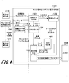
- FIG. 4 is a block diagram showing a detailed configuration example of the partial discharge detection digital signal processing unit 1300 of the partial discharge detection apparatus 1000.
- the partial discharge detection digital signal processing unit 1300 includes a phase zero detection unit 1301, a cycle counter 1302, a high-speed AD data input count counter 1303, a phase counter 1304, a partial discharge information table 1305, and a magnitude determination unit 1306.
- the phase zero detector 1301 detects the phase 0 (phase 0°) of the AC waveform from the AC waveform sample data from the low speed AD converter 1110. After the detection, a reset is output to the phase counter 1304, and the sampling frequency switch 1220 switches the sampling mode signal.
- the cycle counter 1302 counts the cycle of the AC waveform by using the signal from the phase zero detector 1301 and outputs the counted cycle number to the partial discharge information table 1305. Further, the cycle counter 1302 outputs a transmission instruction to transmit all the data in the partial discharge information table 1305 to the communication unit 1400 at a predetermined timing, and then issues an instruction to clear all the data in the partial discharge information table 1305.
- the timing at which the transmission instruction is output from the cycle counter 1302 is, for example, every 10 cycles of the AC waveform.
- the high-speed AD data input number counter 1303 counts the number of times of sampling of partial discharge data (the number of times of data acquisition).
- the phase counter 1304 resets the phase count of the AC waveform by resetting from the phase zero detector 1301 which is output at the timing when the phase 0 of the AC waveform is detected. Then, the phase of the AC waveform is counted using the signal input from the high-speed AD data input number counter 1303.
- the partial discharge information table 1305 is obtained by dividing one cycle of the AC waveform into the digital signal data converted at the first sampling frequency (180 MHz) and the digital signal data converted at the second sampling frequency (200 MHz). Record at every predetermined phase interval.
- a detailed configuration example of the partial discharge information table 1305 will be described later with reference to FIG.
- the size determination unit 1306 compares the data recorded in the partial discharge information table 1305 with the data of the digital signal converted by the high-speed AD converter 1210 at the same phase intervals to determine the size. Then, the size determination unit 1306 determines that the data recorded in the partial discharge information table 1305 is the data of the digital signal converted by the high-speed AD converter 1210, which is determined to be larger than the data recorded in the partial discharge information table 1305. Update.
- the size determination unit 1306 compares the partial discharge sample data from the high-speed AD converter 1210 with the read data in the partial discharge information table 1305 to determine the size of these data. Then, when the sample data of the partial discharge is larger than the read data, the size determining unit 1306 writes the write data for writing the sample data of the partial discharge in the partial discharge information table 1305 (in the figure, “maximum value update write data”). ”) is output. The maximum value of the partial discharge information table 1305 is updated by the write data output from the size determination unit 1306.
- the respective units 1301 to 1306 of the partial discharge detection digital signal processing unit 1300 can be configured by either hardware or computer software.
- each unit 1301 to 1306 is configured by hardware, it is configured by an integrated circuit or the like.
- a processor such as a microcomputer is configured to interpret and execute the program using a program that realizes each function of each unit 1301 to 1306. To do. It is also possible to configure part of each of the units 1301 to 1306 with hardware and the rest with computer software.
- FIG. 5 is an explanatory diagram showing an example of sampling switching timing of the high-speed AD converter 1210.
- the waveform diagram (1) in FIG. 5 shows an example of an AC waveform at a commercial frequency.
- the commercial frequency is, for example, 50 Hz or 60 Hz. In the present embodiment, the commercial frequency will be described as 50 Hz.
- the sampling switching timing (2) in FIG. 5 represents the timing at which the high speed AD converter 1210 switches the sampling frequency.
- the sampling frequency of the high-speed AD converter 1210 is switched to either 180 MHz or 200 MHz for each cycle of the AC waveform of the commercial frequency.
- the high-speed AD converter 1210 performs a process of converting an analog signal into a digital signal at the first sampling frequency (180 MHz) and a process of converting an analog signal into a digital signal at the second sampling frequency (200 MHz). , Are alternately switched at every predetermined cycle of the AC waveform.
- the sampling data (3) in FIG. 5 represents the sampling data of the partial discharge pulse of 180 MHz or 200 MHz output from the high speed AD converter 1210 for each cycle of the AC waveform. Whether the sampling data of 180 MHz and 200 MHz is larger than the maximum value stored in the partial discharge information table 1305 is judged. Then, the data in the partial discharge information table 1305 is updated with the larger value.
- All the data recorded in the partial discharge information table 1305 is passed to the communication unit 1400 and then output to the external network 50 as a partial discharge detection result. Then, the upper-level measuring device 60 receives all the data of the partial discharge information table 1305 via the external network 50 and comprehensively monitors the partial discharge.
- FIG. 6 is an explanatory diagram showing frequency bands at the time of sampling 200 MHz and 180 MHz in the high speed AD converter 1210.
- the first to nth Nyquist boundaries have a band interval of 1 ⁇ 2 of the sampling frequency. That is, the Nyquist boundary appears every 100 MHz in the case of 200 MHz sampling, and appears every 90 MHz in the case of 180 MHz sampling.
- the frequency band of the partial discharge pulse is considered to occur within the range of 50 MHz to 800 MHz. Therefore, the two types of sampling frequencies are set so that the Nyquist boundaries do not overlap with each other in the widest possible band.
- the sampling frequency is set under the condition that the value of the least common multiple of the two types of sampling frequencies 1/2 (the frequency at the Nyquist boundary) is larger than the frequency band of the partial discharge pulse.
- the partial discharge pulse when the partial discharge pulse is 200 MHz, even if the partial discharge pulse cannot be detected under the 200 MHz sampling condition, the partial discharge pulse can be detected under the 180 MHz sampling condition.
- the partial discharge pulse when the partial discharge pulse is 180 MHz, even if the partial discharge pulse cannot be detected under the 180 MHz sampling condition, the partial discharge pulse can be detected under the 200 MHz sampling condition.
- the partial discharge pulse can be reliably observed even with the high-speed AD converter 1210 that does not satisfy the sampling theorem.
- FIG. 7 is a flow chart showing an example of AC waveform phase counting and partial discharge detection processing.
- FIG. 8 is an explanatory diagram showing how the magnitude determination unit 1306 detects partial discharge in one cycle of the AC waveform.
- the phase zero detection unit 1301 is based on the AC waveform sample data input from the low-speed AD converter 1110 for AC waveform acquisition of 50 Hz.
- the phase 0° of the AC waveform is detected.
- the AC waveform 1310 is the zero cross point at the left end.
- phase zero detector 1301 detects a phase of 0°
- the phase zero detector 1301 outputs a reset pulse (initialization pulse) to the phase counter 1304 to initialize the phase counter 1304 ( S11).
- the value of the phase counter 1304 becomes “0”.
- the magnitude determination unit 1306 acquires the maximum detection value corresponding to the phase of the phase counter 1304 from the partial discharge information table 1305 that refers to the phase counter 1304 (S12).
- the phase of the phase counter 1304 is sent to the partial discharge information table 1305 as a reference address.
- the detected maximum value (read data) corresponding to the reference address is acquired from the partial discharge information table 1305 and sent to the size determination unit 1306.
- the partial discharge information table 1305 shows the phase of each 3.75° phase (96 sections) and the maximum detected value of 10 cycles of the AC waveform in the section of the phase. (Maximum charge amount of partial discharge for 10 cycles). Then, the magnitude determination unit 1306 uses the value of the phase (0, 3.75, 7.5,..., 356.25) of the phase counter 1304 as a reference address, and outputs the section of the phase from the partial discharge information table 1305. The maximum detection value (read data) for 10 cycles of the AC waveform is acquired.
- the size determination unit 1306 acquires the input value (charge amount) of the partial discharge from the sample data of the partial discharge acquired from the high-speed AD converter 1210 (S13).
- the input value (charge amount) of the partial discharge is sampled at a 180 MHz sampling interval (5.55 ns) of the high-speed AD converter 1210 or a 200 MHz sampling interval (5 ns) of the high-speed AD converter 1210, as shown in FIG. Represented as a partial discharge pulse signal 1320.
- the size determination unit 1306 compares the detected maximum value of the partial discharge acquired from the partial discharge information table 1305 with the input value (charge amount) of the partial discharge acquired from the high speed AD converter 1210 (S14).
- the maximum value (detection maximum value of the partial discharge information table 1305) ⁇ input value (Yes in S14) the magnitude determination unit 1306 updates the maximum value (detection maximum value) of the partial discharge information table 1305 to the input value. (S15), the process proceeds to step S16.
- the size determination unit 1306 determines whether the value of the sampling frequency is 180 MHz or 200 MHz (S16).
- the magnitude determination unit 1306 determines that the sampling frequency value is 200 MHz, whether the high-speed AD data input number counter 1303 has acquired the input value from the high-speed AD converter 1210 41600 times (phase 3.75° has elapsed). Is confirmed based on the elapsed time (S17).
- the signal may be output from the high-speed AD data input number counter 1303 every time 208 ⁇ s has elapsed.
- step S17 when the high-speed AD data input count counter 1303 acquires the input value of 41600 times (Yes in S17), the process proceeds to step S19. On the other hand, when the high-speed AD data input number counter 1303 has not acquired the input value 41600 times (No in S17), the process returns to step S12 to continue the processing.
- the high-speed AD data input number counter 1303 has acquired the input value of 37444 times from the high-speed AD converter 1210 (phase 3). Whether .75° has elapsed) is confirmed based on the elapsed time (S18).
- the signal may be output from the high-speed AD data input number counter 1303 every time 208 ⁇ s has elapsed.
- step S18 when the high-speed AD data input number counter 1303 acquires the input value of 37444 times (Yes in S18), the process proceeds to step S19. On the other hand, when the high-speed AD data input count counter 1303 has not acquired the input value of 37444 times (No in S18), the process returns to step S12 to continue the processing.
- the steps S12 to S18 are performed. Each step is repeated.
- the maximum value 1330 of the input values (charge amount) of the partial discharge pulse signal 1320 shown in FIG. 8 is compared with the detected maximum value of the partial discharge information table 1305. If the maximum input value 1330 is larger, the maximum detected value in the partial discharge information table 1305 is updated to the maximum input value 1330.
- step S17 the phase counter 1304 is advanced by +3.75° (S19), and the process proceeds to step S12.
- the high-speed AD data input count counter 1303 outputs a 3.75° increment increment signal to the phase counter 1304.
- the phase counter 1304 moves to the next phase section.
- the section moves from the phase 3.75 section to the phase 7.5 section.
- the input value of the partial discharge is acquired and the input value and the detected maximum value of the partial discharge information table 1305 are compared.
- the input value (charge amount) of the partial discharge is detected for each section at a predetermined phase interval of the AC waveform, and each section is detected.
- the maximum value of the electric charge amount of the partial discharge is extracted.
- the phase zero detector 1301 instructs the sampling frequency switch 1220 to switch the sampling mode.
- the sampling mode of the high-speed AD converter 1210 is switched to a sampling mode different from the sampling mode set in the cycle of the previous AC waveform 1310. For example, if the 180 MHz mode is set in the previous cycle, the 200 MHz sampling mode is set in the next cycle. On the contrary, if the 200 MHz sampling mode is set in the previous cycle, the 180 MHz sampling mode is set in the next cycle. Thereafter, the processing shown in FIG. 7 is performed in the switched sampling mode.
- FIG. 9 is a flowchart showing an example of a process of clearing the partial discharge information table 1305 and a process of transmitting the partial discharge information to the communication unit 1400.
- FIG. 10 is an explanatory diagram showing an example of the timing at which the partial discharge information table 1305 is cleared and the timing at which the partial discharge information is transmitted.
- the AC waveform cycle counter 1302 is initialized (S21). At this time, the cycle counter 1302 is initialized to the value "0" as shown in FIG.
- the partial discharge information table 1305 is cleared (S22).
- a table clear signal is sent from the cycle counter 1302 to the partial discharge information table 1305.
- the partial discharge information table 1305 to which the table clear signal has been input is cleared.
- step S23 represents the same process as the detection of the phase 0° described in the uppermost part (starting point) of the flowchart of FIG.
- the process proceeds to step S24, and when the phase 0° is not detected (No in S23), the process returns to the step before step S23.
- step S24 the cycle counter 1302 confirms whether the AC waveform is at the 10th cycle (S24). If the AC waveform is in the 10th cycle (Yes in S24), the process proceeds to step S25. If the AC waveform is not in the 10th cycle (No in S24), the process proceeds to step S26.
- the cycle counter 1302 determines that it is the 10th cycle of the AC waveform (Yes in S24)
- all the data of the partial discharge information table 1305 is transmitted from the partial discharge information table 1305 to the communication unit 1400 (S25).
- the phase zero detector 1301 initializes the cycle counter 1302.
- the value of the cycle counter 1302 is “9” corresponding to the 10th cycle. After that, the cycle counter 1302 is initialized, and the value of the cycle counter 1302 returns to “0” which corresponds to the first cycle.
- the cycle counter 1302 determines that it is not the 10th cycle of the AC waveform (No in S24)
- the AC cycle increment signal from the phase zero detector 1301 is input to the cycle counter 1302 and the cycle counter 1302 is incremented. (S26).
- the value of the cycle counter 1302 is incremented by 1 from 0 to 1, 1 to 2, 2 to 3, and the cycle shifts to the next cycle of the AC waveform.
- steps S23 to S26 are repeated until the AC waveform has passed 10 cycles.
- the cycle of the AC waveform is measured starting from the phase 0° of the AC waveform, and every time 10 cycles of the AC waveform elapse, all the data is transmitted from the partial discharge information table 1305 to the communication unit 1400. Then, the cycle counter 1302 is initialized and the partial discharge information table 1305 is cleared, and then the processing shifts to the next 10 cycles.
- the upper-level measurement device 60 compares the data of the partial discharge information table 1305 received from the communication unit 1400 of the partial discharge detection device 1000 with reference to the partial discharge information table 1305 received in the past. Then, it is determined that the data of the current partial discharge information table 1305 received from the communication unit 1400 is larger than the data of the previously received partial discharge information table 1305 referred to, and the increase in the maximum detection value of the partial discharge is large. If so, the power cable 30 warns that there is a sign of insulation deterioration.
- the reception time of the partial discharge information table 1305 received in the past from the partial discharge detection device 1000 may be arbitrarily set by the user, such as 1 day ago, 1 month ago, 1 year ago, etc. It is preferable to be able to choose. Further, as a criterion for determining that the increase in the maximum detection value of partial discharge is large, for example, a predetermined reference may be selected such that the maximum detection value is double or more.
- FIG. 11 is a flowchart showing an example of a process in which the upper-level measuring device 60 determines whether there is insulation deterioration of the power cable.
- the upper measuring apparatus 60 receives the partial discharge information table 1305. That is, all the data of the partial discharge information table 1305 transmitted from the communication unit 1400 is received by the host measuring device 60.
- the upper-level measuring device 60 refers to the partial discharge information table 1305 received in the past (S31).
- the high-order measuring device 60 compares the data of the table received in the past with the data of the table currently received for each phase of the AC waveform (S32).
- the upper-level measuring device 60 determines whether the increase in the maximum value of the data detected as the partial discharge is large as compared with the past (S33). When it is determined that the increase in the maximum value of the data detected as the partial discharge is large as compared with the past (Yes in S33), the upper-level measuring device 60 outputs a warning "There is a sign of insulation deterioration" (S34). , This process ends.
- the AD converter 1210 in order to prevent the frequency component of the partial discharge pulse from becoming the boundary of the first, second, third and nth Nyquist frequency bands, has two sampling frequencies (180 MHz or 200 MHz). Further, the switching of the sampling frequency is performed at the timing of each cycle of the commercial frequency.
- the high-speed AD converter 1210 observes the partial discharge pulse under conditions that do not satisfy the sampling theorem, and switches between two types of sampling frequencies at the commercial frequency timing. Then, the high speed AD converter 1210 digitizes the analog signal input from the high frequency analog input circuit 1200.
- the size determination unit 1306 compares the partial discharge sample data input from the high frequency analog input circuit 1200 with the read data in the partial discharge information table 1305 to determine the size of the data, and the larger data is used for the partial discharge information.
- the table 1305 is updated. Therefore, the partial discharge information table 1305 allows the digital signal processing unit 1300 for detecting partial discharge to detect the presence or absence of a partial discharge pulse under conditions that do not satisfy the sampling theorem.
- the partial discharge detection apparatus 1000 even if the frequency band of the partial discharge pulse overlaps the Nyquist boundary of the analog signal of the partial discharge current sampled at a certain sampling frequency, another sampling frequency is used.
- the partial discharge pulse can be detected at a position different from the Nyquist boundary of the analog signal sampled by.
- the upper-level measuring device 60 compares the partial discharge information table 1305 received in the past with the partial discharge information table 1305 currently received for each phase of the AC waveform, and detects the partial discharge in comparison with the past. Determine whether the maximum increase in data is large. If there is a large increase in the maximum value of the data, it is possible to issue a warning that there is a sign of insulation deterioration.
- the sampling frequency of the high-speed AD converter 1210 is 180 MHz or 200 MHz, but sampling may be performed at different sampling frequencies other than 180 MHz and 200 MHz. Even in this case, it is desirable that the value of the least common multiple of the values of 1/2 of the two kinds of sampling frequencies be larger than the frequency band of partial discharge.
- FIG. 12 is a block diagram showing a schematic configuration example of a partial discharge detection system 1A configured by using the partial discharge detection device 1000A according to the second embodiment.
- two high frequency analog input circuits 1200 and 1500 are connected to the current measuring device 40.
- the same analog signal is input from the current measuring device 40 to the high frequency analog input circuits 1200 and 1500.
- the analog signal from the high frequency analog input circuit 1200 is input to the first high speed AD converter 1230.
- the first high-speed AD converter 1230 digitizes the analog signal input from the high frequency analog input circuit 1200 at a sampling frequency of 200 MHz based on the sampling clock of 200 MHz input from the 200 MHz oscillator 1240. Then, the AC waveform digital signal digitized at the sampling frequency of 200 MHz is input to the partial discharge detection digital signal processing unit 1300A.
- the digital signal input to the digital signal processing unit 1300A by the first high-speed AD converter 1230 is also referred to as "first sample data of partial discharge".
- the analog signal from the high frequency analog input circuit 1500 is input to the second high speed AD converter 1510.
- the second high-speed AD converter 1510 digitizes the analog signal input from the high frequency analog input circuit 1500 at a sampling frequency of 180 MHz based on the sampling clock of 180 MHz input from the 180 MHz oscillator 1520. Then, the AC waveform digital signal digitized at the sampling frequency of 180 MHz is input to the partial discharge detection digital signal processing unit 1300A.
- the digital signal input to the digital signal processing unit 1300A by the second high-speed AD converter 1510 is also referred to as “second sample data of partial discharge”.
- the partial discharge detection digital signal processing unit 1300A includes a digital signal of an AC waveform of a commercial frequency input from the low-speed AD converter 1110, and a portion input from the first high-speed AD converter 1230 and the second high-speed AD converter 1510, respectively. Digital signal processing for partial discharge detection is performed based on the digital signal of the discharge current. For this reason, the partial discharge detection apparatus 1000A according to the present embodiment does not require the sampling frequency switch 1220 included in the partial discharge detection apparatus 1000 according to the first embodiment.
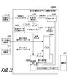
- FIG. 13 is a block diagram showing a detailed configuration example of the partial discharge detection digital signal processing unit 1300A of the partial discharge detection apparatus 1000.
- the partial discharge detection digital signal processing unit 1300A has the same configuration as the partial discharge detection digital signal processing unit 1300 according to the first embodiment, but the data input to the magnitude determination unit 1306A is different. Specifically, the first sample data of partial discharge is input from the first high-speed AD converter 1230 and the second sample data of partial discharge is input from the second high-speed AD converter 1510 to the size determination unit 1306A. It
- the size determination unit 1306A determines whether the value obtained by overlapping the first sample data and the second sample data of the partial discharge or the maximum value read from the partial discharge information table 1305 is larger. When the value obtained by superimposing the first sample data and the second sample data of the partial discharge is larger than the maximum value read from the partial discharge information table 1305, the size determination unit 1306A updates the data of the partial discharge information table 1305.
- FIG. 14 is an explanatory diagram showing an example of sampling data of the first high speed AD converter 1230 and the second high speed AD converter 1510.
- the waveform diagram (1) in FIG. 14 shows an example of an AC waveform at a commercial frequency.
- the commercial frequency is, for example, 50 Hz or 60 Hz.
- the sampling data (2) in FIG. 14 represents the sampling data of the partial discharge pulse sampled by the first high-speed AD converter 1230 at the sampling frequency of 200 MHz.
- the first high-speed AD converter 1230 performs a process of converting an analog signal into a digital signal at the first sampling frequency (200 MHz).
- the sampling data (3) in FIG. 14 represents the sampling data of the partial discharge pulse sampled by the second high-speed AD converter 1510 at the sampling frequency of 180 MHz.
- the second high-speed AD converter 1510 performs a process of converting an analog signal into a digital signal at the second sampling frequency (180 MHz).
- the sampling data (4) in FIG. 14 represents the superimposed 200 MHz sampling data and 180 MHz sampling data.
- the first high-speed AD converter 1230 and the second high-speed AD converter 1510 convert the analog signals into digital signals, respectively, at the same phase intervals obtained by dividing one cycle of the AC waveform.
- the magnitude determination unit 1306A can obtain the maximum value of the sampling data for each phase of the AC waveform of the commercial frequency.
- FIG. 15 is an explanatory diagram showing how the magnitude determination unit 1306A detects partial discharge in one cycle of the AC waveform.
- the values (input values) of the sampling data of 200 MHz and the sampling data of 180 MHz are partially It is compared with the detected maximum value for 10 cycles of the AC waveform acquired from the discharge information table 1305. Then, when the maximum value (detection maximum value of the partial discharge information table 1305) ⁇ input value, the magnitude determination unit 1306A updates the maximum value (detection maximum value) of the partial discharge information table 1305 to the input value.
- the maximum value updated at each phase in one cycle of the AC waveform is read from the partial discharge information table 1305 and sent to the upper measurement device 60 via the communication unit 1400. Then, the upper-level measurement device 60 compares the data of the partial discharge information table 1305 received from the communication unit 1400 of the partial discharge detection device 1000 with the data obtained by referring to the partial discharge information table 1305 received in the past. When it is determined that the maximum value of the data detected as the partial discharge is large as compared with the past, the upper-level measuring device 60 can output the warning “There is a sign of insulation deterioration”.
- the partial discharge detection apparatus 1000A includes the first high-speed AD converter 1230 and the second high-speed AD converter 1510, so that two different types of AC waveforms have the same phase interval. It becomes possible to digitize analog signals at the sampling frequency of. Then, the size determination unit 1306A compares the two types of sample data with the read data in the partial discharge information table 1305 to determine the size of the data. As a result, the digital signal processing unit 1300 for detecting partial discharge can reliably confirm the presence or absence of the partial discharge pulse.
- the specific phase interval of the AC waveform 1310 is a 96-division phase 3.75° section, and the predetermined period of the AC waveform 1310 for extracting the maximum value of the charge amount is 10 cycles.
- the number of divisions of a specific phase interval of the AC waveform and the number of cycles of the AC waveform for extracting the maximum value of the charge amount are not limited to this example, and may be other numbers. Then, the number of divisions of the phase interval and the number of cycles of the AC waveform may be used as parameters to constitute a controllable computer program or the like.
- the number of cycles of the AC waveform for extracting the maximum value of the charge amount is, for example, in accordance with the range of the Nyquist frequency region in which partial discharge is detected, in the case of only the first Nyquist region, one period is defined as the first to The period may be (n ⁇ 2) when confirming the n Nyquist region.
- the process of obtaining the charge amount of the partial discharge from the partial discharge pulse signal 1320 shown in FIGS. 2 and 8 is performed for the entire section (for example, 96 divisions) of a specific phase interval of the AC waveform 1310. (All sections).
- the partial discharge digital signal processing units 1300 and 1300A can also perform the process of obtaining the partial discharge charge amount in a part of a specific phase interval of the AC waveform.
- the partial discharge digital signal processing units 1300 and 1300A calculate the partial discharge charge amount for some sections, when partial discharge occurs in a section where the partial discharge charge amount processing is not performed. Moreover, the generated partial discharge cannot be detected. Therefore, the section for performing the process for obtaining the charge amount of the partial discharge is selected according to the actual frequency of the partial discharge.
- the frequency of partial discharge is high near the zero cross (zero point where the sign of the current amount changes, the phase is 0°, 180°, 360°) of the AC waveform of 50 Hz or 60 Hz, and the partial discharge is distributed before and after the zero cross.
- a predetermined number of sections for example, 50 or 70 sections
- the electric charge amount of the partial discharge may be obtained for.
- the AC signal is converted into the AC signal from the AC waveform digital signal.
- the phase of the waveform is obtained, and the phase of the obtained AC waveform is used to divide the waveform into specific phase intervals.
- the charge amount of partial discharge is obtained for all or a part of the specific phase interval of the AC waveform, and the maximum value of the charge amount is extracted for each predetermined number of cycles. Then, the amount of signal was reduced.
- the method of processing for reducing the amount of a signal of a partial discharge digital signal is not limited to the method of the above-described embodiment and modification, and other methods can be adopted. Even when other methods are adopted, the phase of the AC waveform is obtained from the digital signal of the AC waveform, and the phase of the obtained AC waveform is used to reduce the signal amount of the digital signal of the partial discharge. ..
- the digital signal of the partial discharge can be made to correspond to the phase of the AC waveform, so that the amount of the digital signal of the partial discharge can be detected while more reliably detecting the partial discharge that tends to occur in the vicinity of the zero cross that is the specific phase. It becomes possible to reduce.
- the present invention is not limited to the above-described embodiments, and it goes without saying that various other application examples and modifications can be made without departing from the scope of the present invention described in the claims.
- the above-described embodiment is a detailed and specific description of the configuration of the device and the system in order to explain the present invention in an easy-to-understand manner, and is not necessarily limited to one having all the configurations described.
- part of the configuration of the embodiment described here can be replaced with the configuration of another embodiment, and further, the configuration of another embodiment can be added to the configuration of one embodiment. It is possible.
- the control lines and information lines are shown as being considered necessary for explanation, and not all the control lines and information lines in the product are necessarily shown. In practice, it may be considered that almost all configurations are connected to each other.
- the configuration example in which the Rogowski coil 20 is installed in the power cable 30, the current signal is detected, and the voltage phase information is acquired has been described. Since it is necessary to consider workability and safety when measuring the voltage phase information, the AC voltage signal is taken from the commercial power source that has been voltage-converted via the transformer into the power cable system for partial discharge detection, and the voltage phase It can be realized even if it is acquired as information. A phase shift occurs between the AC voltage signal of the commercial power supply and the AC voltage signal of the cable system due to passing through a transformer, and this phase shift can be corrected by calculation.
- Partial discharge detection system 40... Current measuring device, 60... Upper measurement device, 1000... Partial discharge detection device, 1100... Low frequency analog input circuit, 1110... Low speed AD converter, 1200... High frequency analog input circuit, 1210... High-speed AD converter, 1220... Sampling frequency switcher, 1300... Digital signal processing unit, 1301... Phase zero detection unit, 1302... Cycle counter, 1303... High-speed AD data input frequency counter, 1304... Phase counter, 1305... Partial discharge information Table, 1306... Size determination unit, 1400... Communication unit
Landscapes
- Physics & Mathematics (AREA)
- General Physics & Mathematics (AREA)
- Testing Relating To Insulation (AREA)
Abstract
部分放電検出装置は、電力ケーブルに流れる交流波形のアナログ信号をデジタル信号に変換する低速AD変換器と、2種類の異なるサンプリング周波数毎に規定される複数のナイキスト周波数領域にある、部分放電の電流のアナログ信号をデジタル信号に変換する高速AD変換器と、低速AD変換器で変換された電力ケーブルに流れる交流波形のデジタル信号から求めた交流波形の位相毎に、高速AD変換器で変換された部分放電の電流のデジタル信号から求めた電流値の最大値又は総和に基づいて、部分放電を検出する部分放電検出のデジタル信号処理部と、を備える。
Description
本発明は、部分放電検出装置及び部分放電検出方法に関する。
電力ケーブルの絶縁劣化の兆候を観測するには、電力ケーブルの絶縁物に高電圧を印加した際に発生する、部分放電の電荷量を測定することが一般的である。電力ケーブルの中間接続箱には、ケーブルの絶縁物と接続された接地線がある。部分放電発生時に接地線に流れる電流を、電流測定器(CT:Current Transformer)が測定することが可能である。そして、電流測定器が測定した部分放電発生時の電流は、AD(Analog-to-Digital)変換によりデジタル値に変換され、ケーブルに流れる交流波形の位相に応じて、部分放電の電流が評価される。
例えば、特許文献1には、ケーブルの絶縁物に高電圧を印加した際に発生する部分放電の電荷量を測定することで、ケーブルの絶縁劣化の兆候を観測する技術が開示されている。
電流測定器が測定した部分放電の放電パルスはアナログ信号であるため、AD変換器でアナログ信号をデジタル化する必要がある。部分放電は、微小間隔で発生する高周波パルスのアナログ波形で観測されるため、部分放電の放電パルスを広範囲な周波数帯域で測定することが求められる。また、AD変換器は、サンプリング定理を満たすように動作することが必要である。
しかし、サンプリング定理を満たす条件で、広範囲な周波数帯域のアナログ信号をAD変換器がデジタル化して測定するには、超高速サンプリングが必要となる。超高速サンプリングが可能なAD変換器は非常に高価であり、また、AD変換したデジタルデータも超高速で出力されることとなる。この場合、デジタルデータの信号処理も超高速化が要求される。また、信号処理を実施するFPGA(Field Programmable Gate Array)には、超高速で行われる信号処理に対応するため、高速かつ高価なものが使用される。よって、部分放電パルスを測定するためのハードウェアが高価になってしまう。
そこで、広帯域で発生する部分放電パルスを検出するAD変換器として、サンプリング定理を満たさない条件で、超高速に動作しないAD変換器を採用することが発明者により検討された。サンプリング定理を満たさない条件でアナログ信号をAD変換すると、第1、第2、第3、…、第nナイキストの全ナイキストの周波数帯域に、部分放電パルスが折返しノイズで観測される。部分放電パルスの有無を確認するだけでよければ、折返しノイズが観測されても問題ない。
しかし、サンプリング定理を満たさない条件で行われるAD変換は、第1、第2、第3、…、第nナイキスト境界の周波数帯域におけるSN比(Signal-to-Noise ratio)が著しく悪くなる。仮に、部分放電パルスの周波数帯域がナイキストの境界であった場合、SN比が悪くなるため、部分放電パルスを観測できなかった。
本発明はこのような状況に鑑みて成されたものであり、広い帯域であってもサンプリング定理を満たさない条件で部分放電パルスを検出できるようにすることを目的とする。
本発明は、電力ケーブルにおける部分放電を検出して電力ケーブルの絶縁劣化状態を把握するための部分放電検出装置である。部分放電検出装置は、電力ケーブルに流れる交流波形のアナログ信号をデジタル信号に変換する第1の変換器と、2種類の異なるサンプリング周波数毎に規定される複数のナイキスト周波数領域にある、部分放電の電流のアナログ信号をデジタル信号に変換する第2の変換器と、第1の変換器で変換された電力ケーブルに流れる交流波形のデジタル信号から求めた交流波形の位相毎に、第2の変換器で変換された部分放電の電流のデジタル信号から求めた電流値の最大値又は総和に基づいて、部分放電の発生を検出する信号処理部と、を備える。
本発明によれば、あるサンプリング周波数でサンプリングされた部分放電の電流のアナログ信号のナイキスト境界に部分放電パルスの周波数帯域が重なっていても、別のサンプリング周波数でサンプリングされたアナログ信号のナイキスト境界とは異なる場所で部分放電パルスが検出される。
上記した以外の課題、構成及び効果は、以下の実施の形態の説明により明らかにされる。
上記した以外の課題、構成及び効果は、以下の実施の形態の説明により明らかにされる。
以下、本発明を実施するための形態について、添付図面を参照して説明する。本明細書及び図面において、実質的に同一の機能又は構成を有する構成要素については、同一の符号を付することにより重複する説明を省略する。
[第1の実施の形態]
<部分放電検出システムの構成例>
始めに、本発明の第1の実施の形態に係る部分放電検出システムの構成例について説明する。
図1は、第1の実施の形態に係る部分放電検出装置1000を用いて構成される部分放電検出システム1の概略構成例を示すブロック図である。
<部分放電検出システムの構成例>
始めに、本発明の第1の実施の形態に係る部分放電検出システムの構成例について説明する。
図1は、第1の実施の形態に係る部分放電検出装置1000を用いて構成される部分放電検出システム1の概略構成例を示すブロック図である。
中間接続箱10は、電力ケーブル30同士を接続するように設けられ、接地線により接地されている。接地線には、部分放電を測定する電流測定器(例えば高周波CT)40が取り付けられている。また、電力ケーブル30には、交流波形を測定するロゴスキーコイル20が取り付けられている。
部分放電検出装置1000は、電流測定器40と、ロゴスキーコイル20にそれぞれ接続される。そして、部分放電検出装置1000は、本実施の形態に係る部分放電検出方法を用いて、電力ケーブル30における部分放電を検出して電力ケーブル30の絶縁劣化状態を把握することが可能である。この部分放電検出装置1000は、外部ネットワーク50を介して、上位計測装置60とデータのやりとりを行うように構成されている。
このように、電力ケーブル30と中間接続箱10に対して、ロゴスキーコイル20と電流測定器40と部分放電検出装置1000を設けて、部分放電検出装置1000と上位計測装置60がデータのやりとりを行うように、部分放電検出システム1が構成される。
このように、電力ケーブル30と中間接続箱10に対して、ロゴスキーコイル20と電流測定器40と部分放電検出装置1000を設けて、部分放電検出装置1000と上位計測装置60がデータのやりとりを行うように、部分放電検出システム1が構成される。
部分放電検出装置1000には、電流測定器40とロゴスキーコイル20からそれぞれ出力されたアナログ信号(アナログ値)が入力される。なお、電流測定器40から出力される信号は、部分放電時に接地線に流れる電流信号である。
部分放電検出装置1000は、低周波アナログ入力回路1100、低速AD変換器1110、高周波アナログ入力回路1200、高速AD変換器1210、部分放電検出のデジタル信号処理部1300及び通信部1400を備える。
低周波アナログ入力回路1100には、ロゴスキーコイル20から出力された、商用周波数の交流波形のアナログ信号が入力される。部分放電検出のデジタル信号処理部1300は、この信号から電圧位相情報を取得する。
低速AD変換器1110は、電力ケーブル30に流れる交流波形のアナログ信号をデジタル信号に変換する第1の変換器に相当するものであり、低周波アナログ入力回路1100に入力された、交流波形のアナログ信号をデジタル化する。低速AD変換器1110においてデジタル化された、交流波形のデジタル信号は、部分放電検出のデジタル信号処理部1300に入力される。
低速AD変換器1110は、電力ケーブル30に流れる交流波形のアナログ信号をデジタル信号に変換する第1の変換器に相当するものであり、低周波アナログ入力回路1100に入力された、交流波形のアナログ信号をデジタル化する。低速AD変換器1110においてデジタル化された、交流波形のデジタル信号は、部分放電検出のデジタル信号処理部1300に入力される。
高周波アナログ入力回路1200には、電流測定器40から出力された、部分放電の電流のアナログ信号が入力される。
高速AD変換器1210は、2種類の異なるサンプリング周波数毎に規定される複数のナイキスト周波数領域にある、部分放電の電流のアナログ信号をデジタル信号に変換する第2の変換器に相当するものである。このため、高速AD変換器1210は、高周波アナログ入力回路1200から入力された、部分放電の電流のアナログ信号をデジタル化する。高速AD変換器1210においてデジタル化された、部分放電のデジタル信号は、部分放電検出のデジタル信号処理部1300に入力される。
高速AD変換器1210は、2種類の異なるサンプリング周波数毎に規定される複数のナイキスト周波数領域にある、部分放電の電流のアナログ信号をデジタル信号に変換する第2の変換器に相当するものである。このため、高速AD変換器1210は、高周波アナログ入力回路1200から入力された、部分放電の電流のアナログ信号をデジタル化する。高速AD変換器1210においてデジタル化された、部分放電のデジタル信号は、部分放電検出のデジタル信号処理部1300に入力される。
サンプリング周波数切換器1220は、部分放電検出のデジタル信号処理部1300から入力される切換信号に基づいて、高速AD変換器1210のサンプリングモードを切換える。サンプリングモードは、例えば180MHzモードと200MHzモードとがある。そして、サンプリング周波数切換器1220は、高速AD変換器1210に対してサンプリングモード信号に応じて180MHzと200MHzのいずれかのサンプリングクロックを出力する。
高速AD変換器1210は、サンプリング周波数切換器1220から入力されたサンプリングクロックに従って、交流波形の1周期ごとにサンプリング周波数を切換え、部分放電の電流のアナログ信号を180MHz又は200MHzでサンプリングしてデジタル化する。このように高速AD変換器1210は、2種類の異なるサンプリング周波数として、第1のサンプリング周波数(180MHz)及び第2のサンプリング周波数(200MHz)を用いる。ここで、後述する図6に示すように第1のサンプリング周波数の1/2の値(90MHz)と、第2のサンプリング周波数の1/2の値(100MHz)との最小公倍数の値(900MHz)が、部分放電の周波数帯域(例えば、50MHz~800MHz)より大きい値とする。
部分放電検出のデジタル信号処理部1300は、低速AD変換器1110で変換された電力ケーブル30に流れる交流波形のデジタル信号から求めた交流波形の位相毎に、高速AD変換器1210で変換された部分放電の電流のデジタル信号から求めた電流値の最大値又は総和に基づいて、部分放電の発生を検出する。このため、部分放電検出のデジタル信号処理部1300は、低速AD変換器1110においてデジタル化された交流波形のデジタル信号から交流波形の位相を求める。そして、求めた交流波形の位相情報を用いて、高速AD変換器1210においてデジタル化された部分放電の電流のデジタル信号を処理する。
通信部1400は、図4に示す部分放電情報テーブル1305に記録されたデータ(部分放電の検出結果)を、外部ネットワーク50に接続され、部分放電を監視する上位計測装置60に出力する。上位計測装置60に出力されるデータは、該部分放電情報テーブル1305に記録された全データであるが、一部のデータだけとしてもよい。
また、中間接続箱10で接続された、多数の電力ケーブル30の全体に対して、複数の部分放電検出装置1000が設けられる。上位計測装置60は、外部ネットワーク50を介して、複数の部分放電検出装置1000の検出結果を、総合的に監視し、電力ケーブル30の絶縁劣化の兆候を判断する。
部分放電検出装置1000では、ベースバンド・サンプリング方式とアンダー・サンプリング方式を併用して、高速AD変換器1210におけるアナログ・デジタル変換を行う。ここで、ベースバンド・サンプリング方式は、第1ナイキスト周波数帯域0~1/2・Fs(サンプリング周波数)を、デジタル化可能なアナログ入力帯域としている。アンダー・サンプリング方式は、サンプリング周波数よりも高周波帯域のアナログ入力に対応するもので、第1以外の、第2、第3、…第nナイキスト周波数帯域(n-1)/2~n/2・Fsといった特定のナイキスト周波数帯域に限定した、サンプリング方式である。そして、ベースバンド・サンプリング方式とアンダー・サンプリング方式を併用することで、高周波アナログ入力回路1200が、広帯域のアナログ信号を高速AD変換器1210に入力させることが可能となる。
次に、第1の実施の形態に係る部分放電のデータの処理方法について、図2と図3を参照して説明する。
図2は、部分放電のデータの処理に使用される、測定された電流の交流波形の特定の位相間隔の区間分けと、1つの区間の例を示す拡大図である。図2に示すチャートは、横軸を位相、縦軸を電圧として表される。
図2は、部分放電のデータの処理に使用される、測定された電流の交流波形の特定の位相間隔の区間分けと、1つの区間の例を示す拡大図である。図2に示すチャートは、横軸を位相、縦軸を電圧として表される。
交流波形1310の特定の位相間隔で規定される1つの区間において、部分放電検出のデジタル信号処理部1300は、デジタル化した信号から、部分放電のその区間の電荷量を求める。この電荷量として、部分放電パルス信号1320の総和、又は、部分放電パルス信号1320の最大値1330が求められる。同様に、部分放電検出のデジタル信号処理部1300は、特定の位相間隔の全ての区間において、各区間の電荷量として、部分放電パルス信号1320の総和又は最大値1330を求める。
特定の位相間隔は、50Hz又は60Hzの交流波形の1周期360°を、所定数で分割して求められる。例えば、1周期360°を96区間に分割することで、1つの区間を3.75°の位相間隔とすることができる。なお、図2では、図示の都合により、便宜的に、交流波形の1周期を20区間に分割しているが、図2の20区間に限定されるものではない。
また、交流波形1310としては、低速AD変換器1110において交流波形のアナログ信号からデジタル化された、交流波形のデジタル信号を用いる。そして、交流波形のデジタル信号から交流波形の位相を求めて、求めた交流波形の位相を用いて、図2に示したように、特定の位相間隔に分割する。
上述したように、部分放電検出のデジタル信号処理部1300は、特定の位相間隔の全ての区間において、部分放電の電荷量として、部分放電パルス信号1320の総和又は最大値を求める。そして、部分放電検出のデジタル信号処理部1300における信号処理によって、求めた部分放電の電荷量のデータを間引く。
そこで、部分放電検出のデジタル信号処理部1300における信号処理は、交流波形の所定周期中において、特定の位相間隔の全区間の部分放電の電荷量(部分放電パルス信号1320の振幅の総和又は最大値)のうち、最大値の電荷量のみを抽出して記録する。これにより、位相間隔の全区間の所定周期数のデジタルデータが、最大値の電荷量を表す1つのデータに間引かれる。交流波形の所定周期は、例えば、5周期~20周期の範囲から選定される。
例えば、前述した1周期360°を96区間に分割して電荷量を求めて、交流波形の所定周期を10周期とした場合には、96×10=960個の部分放電の電荷量のデータが記録される。このため、部分放電検出のデジタル信号処理部1300は、部分放電の電荷量の最大値を表す1個のデータだけが残るように、他のデータを間引く。
上述したように位相間隔の全区間の所定周期数のデジタルデータを1つの最大値の電荷量に間引いても、間引いた後の最大値の電荷量が部分放電の有無に応じて変化するので、最大値の電荷量に部分放電の有無が反映される。従って、最大値の電荷量によって、部分放電の有無を検出することができる。
このように部分放電検出のデジタル信号処理部1300は、データを間引いて、残ったデータ(抽出した最大値の電荷量のデータ)を、通信部1400から外部ネットワーク50を介して、上位計測装置60に送信する。
上位計測装置60では、外部ネットワーク50から受信したデータ(最大値の電荷量のデータ)の推移を監視する。上位計測装置60において、最大値の電荷量の推移を監視することにより、電力ケーブル30の絶縁劣化の兆候を監視することができる。また、既設の電力ケーブル30の劣化の状態を調べて、寿命を予測することができる。
そして、上位計測装置60において、受信した現在の部分放電の最大の電荷量のデータと、過去に受信した部分放電の最大の電荷量のデータとの比較を、継続的に行うようにすれば、多数の電力ケーブル30全体の劣化の進行状況を随時把握することができる。
そして、上位計測装置60において、受信した現在の部分放電の最大の電荷量のデータと、過去に受信した部分放電の最大の電荷量のデータとの比較を、継続的に行うようにすれば、多数の電力ケーブル30全体の劣化の進行状況を随時把握することができる。
以上説明した部分放電のデータの処理方法を、フローチャートにまとめて図3に示す。
図3は、部分放電のデータの処理方法の例を示すフローチャートである。
図3は、部分放電のデータの処理方法の例を示すフローチャートである。
始めに、部分放電検出のデジタル信号処理部1300は、交流波形の特定の位相間隔の区間毎の電流の最大値又は総和を全ての区間で求め、これを各区間の電荷量とする(S1)。
次に、部分放電検出のデジタル信号処理部1300は、交流波形の所定周期数毎に、区間の電荷量の最大値を抽出する(S2)。これにより、(1周期の区間数×周期数)個のデータが1個のデータに間引かれる。
次に、部分放電検出のデジタル信号処理部1300は、交流波形の所定周期数毎に、区間の電荷量の最大値を抽出する(S2)。これにより、(1周期の区間数×周期数)個のデータが1個のデータに間引かれる。
次に、部分放電検出のデジタル信号処理部1300は、抽出した電荷量の最大値のデータを、通信部1400を介して上位計測装置60に送信する(S3)。
このようにして、抽出により間引いたデータが上位計測装置60に送信されるので、上位計測装置60に送るデータの量を減らすことができる。
このようにして、抽出により間引いたデータが上位計測装置60に送信されるので、上位計測装置60に送るデータの量を減らすことができる。
部分放電検出装置1000は、電力ケーブル30に常時設置されており、電力ケーブル30の状態を監視する。そして、部分放電検出装置1000は、データを間引いて、上位計測装置60に送るデータの量を減らすことにより、部分放電検出のデジタル信号処理部1300のコストや消費電力を低減することができる。これにより、部分放電検出装置1000の常時設置を実現することが可能になる。
なお、図1に示した低周波アナログ入力回路1100、高周波アナログ入力回路1200、低速AD変換器1110、高速AD変換器1210、部分放電検出のデジタル信号処理部1300は、ハードウェア又はコンピュータソフトウェアのいずれでも構成することが可能である。
各処理部をハードウェアで構成する場合には、部分放電検出装置1000内に設けられた集積回路等で構成する。
各処理部をコンピュータソフトウェアで構成する場合には、アナログ入力回路、AD変換器、部分放電検出のデジタル信号処理部のそれぞれの機能を実現するプログラムをマイクロコンピュータ等のプロセッサが解釈して、実行可能となるように構成する。
また、一部をハードウェアで構成して、残りをコンピュータソフトウェアで構成することも可能である。
各処理部をハードウェアで構成する場合には、部分放電検出装置1000内に設けられた集積回路等で構成する。
各処理部をコンピュータソフトウェアで構成する場合には、アナログ入力回路、AD変換器、部分放電検出のデジタル信号処理部のそれぞれの機能を実現するプログラムをマイクロコンピュータ等のプロセッサが解釈して、実行可能となるように構成する。
また、一部をハードウェアで構成して、残りをコンピュータソフトウェアで構成することも可能である。
より好ましくは、図1に示した低周波アナログ入力回路1100、高周波アナログ入力回路1200、低速AD変換器1110、高速AD変換器1210、部分放電検出のデジタル信号処理部1300をハードウェアで構成する。
これらの処理部をコンピュータソフトウェアで構成した場合には、計算結果等を記憶するメモリが必要になり、ソフトウェアの起動やメモリの動作のための電力も必要となる。
これに対して、ハードウェアで構成した場合には、ソフトウェアの起動やメモリの動作のための電力は不要であるため、コンピュータソフトウェアで構成した場合と比較して、部分放電検出装置1000の動作に必要な電力を少なくすることができる。これにより、多数の電力ケーブル30全体に対して、より多くの部分放電検出装置1000を設置することが可能になる。
これらの処理部をコンピュータソフトウェアで構成した場合には、計算結果等を記憶するメモリが必要になり、ソフトウェアの起動やメモリの動作のための電力も必要となる。
これに対して、ハードウェアで構成した場合には、ソフトウェアの起動やメモリの動作のための電力は不要であるため、コンピュータソフトウェアで構成した場合と比較して、部分放電検出装置1000の動作に必要な電力を少なくすることができる。これにより、多数の電力ケーブル30全体に対して、より多くの部分放電検出装置1000を設置することが可能になる。
そして、高周波アナログ入力回路1200の折返しノイズフィルタの特性により、後述する図6に示すように複数のナイキスト周波数領域のアナログ信号を通過させることができる。そして、高速AD変換器1210において、複数のナイキスト周波数領域のアナログ信号に対して、デジタル信号への変換が行われる。これにより、複数のナイキスト周波数領域という広帯域(例えば、50MHz~800MHz)のアナログ信号をデジタル信号に変換するので、広帯域にわたって発生する部分放電を検出することができる。
また、複数のナイキスト周波数領域のアナログ信号を変換するので、第1ナイキスト周波数領域のアナログ信号を変換するベースバンド・サンプリング方式と比較して、サンプリング周波数を低減することができる。これにより、高速AD変換器1210とデジタル信号処理部1300に高価な部品を使用する必要がなく、比較的安価な部品で高速AD変換器1210とデジタル信号処理部1300を構成することができる。このため、比較的安価な部品を組み合わせて、部分放電を検出するための構成を実現することが可能である。
また、部分放電検出のデジタル信号処理部1300は、交流波形の1周期を所定の位相間隔に分割して、所定の位相間隔の全区間について、部分放電の電荷量(部分放電の電流値の最大値又は総和)を求める。これにより、高速AD変換器1210においてデジタル変換した部分放電の電流のデジタル信号の全体の信号から、部分放電の電荷量(電流の最大値又は総和)の信号になるため、信号の量が低減される。
さらに、部分放電検出のデジタル信号処理部1300は、全区間の交流波形の所定の周期数毎における部分放電の電荷量の最大値を抽出する。これにより、(区間数×所定の周期数)の個数の電荷量の信号が、最大値の電荷量の1個の信号に間引かれて、信号の量が低減される。
このように、部分放電検出のデジタル信号処理部1300が、高速AD変換器1210においてデジタル変換された、部分放電の電流の信号の量を低減する処理を行っている。これにより、複数のナイキスト周波数領域という広範囲の周波数領域の信号を取り扱っていても、処理の後の信号の量が少なくなる。信号の量が少なくなるので、信号を記憶するための構成(メモリ等)の簡略化、通信部1400から外部ネットワーク50にデータを送信する際のオーバーフローの防止、部分放電検出装置1000の消費電力の低減、等を実現することが可能になる。
また、低速AD変換器1110においてデジタル変換された、交流波形のデジタル信号から交流波形の位相を求め、この交流波形の位相を用いて所定位相間隔の区間に分割して、部分放電の信号の低減を行っている。交流波形の位相を用いることにより、広範囲の周波数領域の信号から、容易に信号の量を低減することができる。
また、通信部1400から外部ネットワーク50に送信する際に、オーバーフローを防止することができることにより、上位計測装置60において、リアルタイムで確実に部分放電の発生を把握することが可能になる。
部分放電検出装置1000の消費電力を低減できることにより、多数の電力ケーブル30全体に対して、より多くの部分放電検出装置1000を設置することが可能になる。また、部分放電検出装置を測定したい箇所に移動させることが主体であった、従来の検出方法に対して、多数の部分放電検出装置1000を据え置きで設置して、上位計測装置60において部分放電の発生を常時監視することが可能になる。
そして、第1の実施の形態では、高速AD変換器1210においてデジタル変換した部分放電の電流のデジタル信号の全体の信号から、交流波形の所定の周期数毎に最大値の電荷量の1個の信号に低減されるので、信号の量が大幅に低減される。これにより、信号を記憶するための構成(メモリ等)の簡略化や、部分放電検出装置1000の消費電力の低減の効果が大きくなり、部分放電検出装置1000の構成の簡略化や部品コストの低減を図ることが可能になる。
さらに、部分放電検出装置1000が通信部1400を備え、通信部1400が外部ネットワーク50を介して上位計測装置60と接続され、通信部1400からデータを送信するように構成している。これにより、部分放電検出装置1000と上位計測装置60とを有線で接続した場合と比較して、部分放電検出装置1000の設置の自由度が高まり、多数の電力ケーブル30全体に対して、より多くの部分放電検出装置1000を設置することが可能になる。
<部分放電検出のデジタル信号処理部の構成例>
図4は、部分放電検出装置1000の部分放電検出のデジタル信号処理部1300の詳細な構成例を示すブロック図である。
図4は、部分放電検出装置1000の部分放電検出のデジタル信号処理部1300の詳細な構成例を示すブロック図である。
部分放電検出のデジタル信号処理部1300は、位相ゼロ検出部1301、周期カウンタ1302、高速ADデータ入力回数カウンタ1303、位相カウンタ1304、部分放電情報テーブル1305及び大小判定部1306を有する。
位相ゼロ検出部1301は、低速AD変換器1110からの交流波形サンプルデータから、交流波形の位相0(位相0°)を検出する。検出後は位相カウンタ1304にリセットを出力すると共に、サンプリング周波数切換器1220にサンプリングモード信号の切換を実施する。
周期カウンタ1302は、位相ゼロ検出部1301からの信号を用いて、交流波形の周期をカウントし、カウントした周期数を部分放電情報テーブル1305に出力する。また、周期カウンタ1302は、所定のタイミングで部分放電情報テーブル1305の全データを通信部1400に送信する送信指示を出力し、その後、部分放電情報テーブル1305の全データをクリアする指示を行う。周期カウンタ1302から送信指示が出力されるタイミングは、例えば、交流波形の10周期毎である。
高速ADデータ入力回数カウンタ1303は、部分放電のデータのサンプリング回数(データ取得回数)をカウントする。
位相カウンタ1304は、交流波形の位相0が検出されたタイミングで出力される位相ゼロ検出部1301からリセットにより、交流波形の位相カウントをリセットする。その後、高速ADデータ入力回数カウンタ1303から入力する信号を用いて、交流波形の位相をカウントする。
位相カウンタ1304は、交流波形の位相0が検出されたタイミングで出力される位相ゼロ検出部1301からリセットにより、交流波形の位相カウントをリセットする。その後、高速ADデータ入力回数カウンタ1303から入力する信号を用いて、交流波形の位相をカウントする。
部分放電情報テーブル1305は、第1のサンプリング周波数(180MHz)で変換されたデジタル信号のデータ、及び第2のサンプリング周波数(200MHz)で変換されたデジタル信号のデータを交流波形の1周期を分割した所定の位相間隔毎に記録する。部分放電情報テーブル1305の詳細な構成例は、後述する図8にて説明する。
大小判定部1306は、部分放電情報テーブル1305に記録されたデータと、高速AD変換器1210により変換されたデジタル信号のデータとを同じ位相間隔毎に比較して大小判定を行う。そして、大小判定部1306は、部分放電情報テーブル1305に記録されたデータより大きいと判定した、高速AD変換器1210により変換されたデジタル信号のデータにより、部分放電情報テーブル1305に記録されたデータを更新する。
例えば、大小判定部1306は、高速AD変換器1210からの部分放電のサンプルデータと、部分放電情報テーブル1305内のリードデータとを比較して、これらのデータの大小を判定する。そして、大小判定部1306は、部分放電のサンプルデータがリードデータより大きい場合に、部分放電のサンプルデータを部分放電情報テーブル1305に書込むためのライトデータ(図中では、「最大値更新ライトデータ」と記載)を出力する。大小判定部1306から出力されたライトデータにより部分放電情報テーブル1305の最大値が更新される。
なお、部分放電検出のデジタル信号処理部1300の各部1301~1306は、ハードウェア又はコンピュータソフトウェアのいずれでも構成することが可能である。
各部1301~1306をハードウェアで構成する場合には、集積回路等で構成する。
また、各部1301~1306をコンピュータソフトウェアで構成する場合には、各部1301~1306のそれぞれの機能を実現するプログラムを使用して、マイクロコンピュータ等のプロセッサがプログラムを解釈して、実行するように構成する。
また、各部1301~1306の一部をハードウェアで構成して、残りをコンピュータソフトウェアで構成することも可能である。
各部1301~1306をハードウェアで構成する場合には、集積回路等で構成する。
また、各部1301~1306をコンピュータソフトウェアで構成する場合には、各部1301~1306のそれぞれの機能を実現するプログラムを使用して、マイクロコンピュータ等のプロセッサがプログラムを解釈して、実行するように構成する。
また、各部1301~1306の一部をハードウェアで構成して、残りをコンピュータソフトウェアで構成することも可能である。
<サンプリング切換タイミング>
図5は、高速AD変換器1210のサンプリング切換タイミングの例を示す説明図である。
図5は、高速AD変換器1210のサンプリング切換タイミングの例を示す説明図である。
図5の波形図(1)は、商用周波数の交流波形の例を表す。商用周波数は、例えば、50Hz又は60Hzである。本実施の形態では、商用周波数を50Hzとして説明する。
図5のサンプリング切換タイミング(2)は、高速AD変換器1210がサンプリング周波数を切替えるタイミングを表す。商用周波数の交流波形の1周期毎に、高速AD変換器1210のサンプリング周波数が、180MHz又は200MHzのいずれかに切換えられる。このように高速AD変換器1210は、第1のサンプリング周波数(180MHz)でアナログ信号をデジタル信号に変換する処理と、第2のサンプリング周波数(200MHz)でアナログ信号をデジタル信号に変換する処理とを、交流波形の所定の周期毎に交互に切換える。
図5のサンプリングデータ(3)は、交流波形の1周期毎に高速AD変換器1210から出力される180MHz又は200MHzの部分放電パルスのサンプリングデータを表す。180MHzと200MHzのサンプリングデータは、部分放電情報テーブル1305に記憶される最大値よりも大きいか否かを判定する大小判定が実施される。そして、大きい方の値で、部分放電情報テーブル1305のデータが更新される。
部分放電情報テーブル1305に記録される全データは、通信部1400に渡された後、部分放電検出結果として外部ネットワーク50に出力される。そして、上位計測装置60が、外部ネットワーク50を介して部分放電情報テーブル1305の全データを受信して、総合的に部分放電の監視を実施する。
図6は、高速AD変換器1210における200MHzと180MHzサンプリング時の周波数帯域を示す説明図である。第1~第nのナイキスト境界は、サンプリング周波数の1/2の帯域間隔となる。即ち、ナイキストの境界は、例えば200MHzサンプリングの場合に100MHz毎に現れ、180MHzサンプリングの場合に90MHz毎に現れる。
図6の上段に示すように、部分放電パルスの周波数帯域は、50MHz~800MHzの範囲内で発生すると考えられる。このため、2種類のサンプリング周波数は、できるだけ広帯域でナイキスト境界が重複しないように設定される。ここで、サンプリング周波数の設定は、2種類のサンプリング周波数1/2(ナイキスト境界の周波数)の最小公倍数の値が、部分放電パルスの周波数帯域より大きい条件に設定する。
例えば部分放電パルスが200MHzであった場合、200MHzサンプリング条件では、部分放電パルスを検出できなくても、180MHzサンプリング条件では部分放電パルスを検出できる。逆に、部分放電パルスが180MHzであった場合、180MHzサンプリング条件では、部分放電パルスを検出できなくても、200MHzサンプリング条件では、部分放電パルスを検出できる。
以上により、サンプリング定理を満たさない高速AD変換器1210であっても、確実に部分放電パルスを観測することができる。
以上により、サンプリング定理を満たさない高速AD変換器1210であっても、確実に部分放電パルスを観測することができる。
<交流波形の位相のカウント処理、及び部分放電の検出処理>
次に、部分放電のデータの処理方法のうちの、交流波形の位相のカウントと、部分放電の検出について、図7及び図8を参照して説明する。
図7は、交流波形の位相のカウントと、部分放電の検出処理の例を示すフローチャートである。
図8は、交流波形の1周期で大小判定部1306が部分放電を検出する様子を示す説明図である。
次に、部分放電のデータの処理方法のうちの、交流波形の位相のカウントと、部分放電の検出について、図7及び図8を参照して説明する。
図7は、交流波形の位相のカウントと、部分放電の検出処理の例を示すフローチャートである。
図8は、交流波形の1周期で大小判定部1306が部分放電を検出する様子を示す説明図である。
始めに、図7の最上部(即ち、開始時点)に示すように、位相ゼロ検出部1301が、50Hzの交流波形取得用の低速AD変換器1110から入力される交流波形サンプルデータに基づいて、交流波形の位相0°を検出する。
この時、図8に示すように、交流波形1310が左端のゼロクロス点となっている。
この時、図8に示すように、交流波形1310が左端のゼロクロス点となっている。
次に、位相ゼロ検出部1301が位相0°を検出したときに、位相ゼロ検出部1301から位相カウンタ1304へ、リセットパルス(初期化のパルス)を出力して、位相カウンタ1304を初期化する(S11)。この時、図8の左上に示すように、位相カウンタ1304の値が「0」になる。
次に、大小判定部1306は、位相カウンタ1304を参照する部分放電情報テーブル1305より、位相カウンタ1304の位相に対応する検出最大値を取得する(S12)。ここで、位相カウンタ1304の位相が参照アドレスとして部分放電情報テーブル1305に送られる。そして、参照アドレスに対応する検出最大値(リードデータ)が部分放電情報テーブル1305から取得され、大小判定部1306に送られる。
部分放電情報テーブル1305は、図8の右下に示すように、位相の3.75°毎の区間(96個の区間)の位相と、その位相の区間の交流波形10周期分の検出最大値(10周期分の部分放電の電荷量の最大値)とから構成されている。そして、大小判定部1306は、位相カウンタ1304の位相(0,3.75,7.5,・・・,356.25)の値を参照アドレスとして、部分放電情報テーブル1305から、その位相の区間の交流波形10周期分の検出最大値(リードデータ)を取得する。
次に、大小判定部1306は、高速AD変換器1210より取得した部分放電のサンプルデータから部分放電の入力値(電荷量)を取得する(S13)。部分放電の入力値(電荷量)は、図8に示すように、高速AD変換器1210の180MHzのサンプリング間隔(5.55ns)、又は高速AD変換器1210の200MHzのサンプリング間隔(5ns)でサンプリングされた、部分放電パルス信号1320として表される。
次に、大小判定部1306は、部分放電情報テーブル1305より取得した部分放電の検出最大値と、高速AD変換器1210より取得した部分放電の入力値(電荷量)を比較する(S14)。最大値(部分放電情報テーブル1305の検出最大値)<入力値の場合(S14のYes)、大小判定部1306は、部分放電情報テーブル1305の最大値(検出最大値)を入力値に更新して(S15)、ステップS16に進む。
最大値(部分放電情報テーブル1305の検出最大値)≧入力値の場合(S14のNo)、部分放電情報テーブル1305の更新は行われない。そして、S14のNo、又はステップS15の処理の後、大小判定部1306は、サンプリング周波数の値が、180MHz又は200MHzのいずれであるかを判定する(S16)。
大小判定部1306により、サンプリング周波数の値が200MHzと判定された場合、高速ADデータ入力回数カウンタ1303は、高速AD変換器1210から41600回入力値を取得したか(位相3.75°を経過したか)を、経過時間に基づいて確認する(S17)。
ここで、入力値の回数=(経過時間/サンプリング間隔5ns)であり、41600回の入力値となるのは約208μsである。このため、208μs経過する毎に、高速ADデータ入力回数カウンタ1303から信号を出力すればよい。
そして、高速ADデータ入力回数カウンタ1303は、41600回入力値を取得した場合(S17のYes)、ステップS19に進む。一方、高速ADデータ入力回数カウンタ1303は、41600回入力値を取得していない場合(S17のNo)、ステップS12に戻って処理を続ける。
一方、ステップS16にて大小判定部1306により、サンプリング周波数の値が180MHzと判定された場合、高速ADデータ入力回数カウンタ1303は、高速AD変換器1210から37444回入力値を取得したか(位相3.75°を経過したか)を、経過時間に基づいて確認する(S18)。
ここで、入力値の回数=(経過時間/サンプリング間隔5.55ns)であり、37444回の入力値となるのは約208μsである。このため、208μs経過する毎に、高速ADデータ入力回数カウンタ1303から信号を出力すればよい。
そして、高速ADデータ入力回数カウンタ1303は、37444回入力値を取得した場合(S18のYes)、ステップS19に進む。一方、高速ADデータ入力回数カウンタ1303は、37444回入力値を取得していない場合(S18のNo)、ステップS12に戻って処理を続ける。
このように、サンプリング周波数の値が、180MHzであれば37444回、サンプリング周波数の値が、200MHzであれば41600回、高速ADデータ入力回数カウンタ1303が入力値を取得するまで、ステップS12~S18の各ステップが繰り返される。これにより、図8に示す部分放電パルス信号1320の入力値(電荷量)のうちの最大値1330を、部分放電情報テーブル1305の検出最大値と比較することになる。そして、入力値の最大値1330の方が大きければ、部分放電情報テーブル1305の検出最大値が入力値の最大値1330に更新される。
ステップS17のYes、又はステップS18のYesの後、位相カウンタ1304を+3.75°進め(S19)、ステップS12に進む。この時、高速ADデータ入力回数カウンタ1303から、位相カウンタ1304へ、3.75°経過インクリメントの信号を出力する。
この時、図8においては、位相カウンタ1304が、次の位相の区間に移る。例えば位相3.75の区間から位相7.5の区間に移る。
そして、次の位相の区間について、部分放電の入力値の取得、及び、入力値と部分放電情報テーブル1305の検出最大値の比較が実行される。このようにして、交流波形の位相のカウントと、部分放電の検出が実行されることにより、交流波形の所定位相間隔の各区間について、部分放電の入力値(電荷量)が検出され、各区間の部分放電の電荷量の最大値が抽出される。
さらに、交流波形1310の次の周期では、位相ゼロ検出部1301がサンプリングモードの切換えをサンプリング周波数切換器1220に指示する。そして、高速AD変換器1210のサンプリングモードが、前の交流波形1310の周期で設定されていたサンプリングモードとは異なるサンプリングモードに切換わる。例えば、前の周期で180MHzモードが設定されていれば、次の周期で200MHzのサンプリングモードが設定される。逆に、前の周期で200MHzのサンプリングモードが設定されていれば、次の周期で180MHzのサンプリングモードが設定される。その後、切換わったサンプリングモードにより、図7に示した処理が行われる。
<部分放電情報テーブルのクリアと、部分放電情報の通信部への送信処理>
次に、部分放電のデータの処理方法のうちの、部分放電情報テーブル1305のクリアと、部分放電情報の通信部1400への送信について、図4、図9及び図10を参照して説明する。
図9は、部分放電情報テーブル1305をクリアする処理と、部分放電情報の通信部1400への送信処理の例を示すフローチャートである。
図10は、部分放電情報テーブル1305がクリアされるタイミングと、部分放電情報が送信されるタイミングの例を示す説明図である。
次に、部分放電のデータの処理方法のうちの、部分放電情報テーブル1305のクリアと、部分放電情報の通信部1400への送信について、図4、図9及び図10を参照して説明する。
図9は、部分放電情報テーブル1305をクリアする処理と、部分放電情報の通信部1400への送信処理の例を示すフローチャートである。
図10は、部分放電情報テーブル1305がクリアされるタイミングと、部分放電情報が送信されるタイミングの例を示す説明図である。
始めに、交流波形の周期カウンタ1302が初期化される(S21)。この時、周期カウンタ1302は、図10に示すように、値「0」に初期化される。
次に、部分放電情報テーブル1305がクリアされる(S22)。この時、周期カウンタ1302から部分放電情報テーブル1305へ、テーブルクリアの信号が送られる。そして、図10に示すように、テーブルクリアの信号が入力された、部分放電情報テーブル1305がクリアされる。
次に、位相ゼロ検出部1301は、交流波形の位相0°を検出したかを確認する(S23)。このステップS23は、図7のフローチャートの最上部(開始時点)に記載された、位相0°の検出と同じ処理を表す。位相ゼロ検出部1301が位相0°を検出した場合(S23のYes)、ステップS24に進み、位相0°を検出していない場合(S23のNo)、ステップS23の前に戻る。
次に、ステップS23のYesの場合、周期カウンタ1302は、交流波形が10周期目であるかを確認する(S24)。交流波形が10周期目である場合(S24のYes)、ステップS25に進み、交流波形が10周期目ではない場合(S24のNo)、ステップS26に進む。
周期カウンタ1302が、交流波形の10周期目と判定した場合(S24のYes)、部分放電情報テーブル1305から、部分放電情報テーブル1305の全データが通信部1400に送信される(S25)。その後、位相ゼロ検出部1301は、周期カウンタ1302を初期化する。
この時、図10では、周期カウンタ1302の値が10周期目に当たる「9」である。その後、周期カウンタ1302が初期化されることにより、周期カウンタ1302の値が1周期目に当たる「0」に戻る。
また、周期カウンタ1302を初期化し、部分放電情報テーブル1305をクリアする前に、通信部1400に送信した部分放電情報テーブル1305の全データが通信部1400から上位計測装置60へ送信される。そして、周期カウンタ1302を初期化する際に、部分放電情報テーブル1305のクリアも実行される。
周期カウンタ1302が、交流波形の10周期目ではないと判定した場合(S24のNo)、位相ゼロ検出部1301からの交流周期インクリメントの信号が、周期カウンタ1302に入力されて、周期カウンタ1302がインクリメントされる(S26)。この時、図10に示すように、周期カウンタ1302の値が、0から1、1から2、2から3と、1つ増えて、交流波形の次の周期に移行する。
このように、交流波形が10周期を経過するまで、ステップS23~S26の各ステップが繰り返される。これにより、交流波形の位相0°を起点として交流波形の周期が計測され、交流波形の10周期が経過する毎に、部分放電情報テーブル1305から全データが通信部1400に送信される。そして、周期カウンタ1302が初期化され、部分放電情報テーブル1305がクリアされた後、次の10周期における処理に移行する。
<上位計測装置におけるデータの推移の監視>
次に、上位計測装置60におけるデータの推移の監視について説明する。
上位計測装置60は、部分放電検出装置1000の通信部1400から受信した部分放電情報テーブル1305のデータを、過去に受信した部分放電情報テーブル1305を参照して、比較を行う。そして、通信部1400から受信した、現在の部分放電情報テーブル1305のデータが、参照した過去に受信した部分放電情報テーブル1305のデータと比較して、部分放電の検出最大値の増加が大きいと判定した場合には、電力ケーブル30に絶縁劣化の兆候があることを警告する。
次に、上位計測装置60におけるデータの推移の監視について説明する。
上位計測装置60は、部分放電検出装置1000の通信部1400から受信した部分放電情報テーブル1305のデータを、過去に受信した部分放電情報テーブル1305を参照して、比較を行う。そして、通信部1400から受信した、現在の部分放電情報テーブル1305のデータが、参照した過去に受信した部分放電情報テーブル1305のデータと比較して、部分放電の検出最大値の増加が大きいと判定した場合には、電力ケーブル30に絶縁劣化の兆候があることを警告する。
なお、上位計測装置60が参照する、過去に部分放電検出装置1000から受信した部分放電情報テーブル1305の受信時期は、ユーザーの設定により、1日前、1ヶ月前、1年前、等々、任意に選べるようにすることが好ましい。
また、部分放電の検出最大値の増加が大きいと判定する基準としては、例えば、検出最大値が2倍以上になる等、所定の基準を選定すればよい。
また、部分放電の検出最大値の増加が大きいと判定する基準としては、例えば、検出最大値が2倍以上になる等、所定の基準を選定すればよい。
<電力ケーブルの絶縁劣化の有無の判定方法>
次に、電力ケーブルの絶縁劣化の有無の判定方法について、説明する。
図11は、上位計測装置60が電力ケーブルの絶縁劣化の有無を判定する処理の例を示すフローチャートである。
次に、電力ケーブルの絶縁劣化の有無の判定方法について、説明する。
図11は、上位計測装置60が電力ケーブルの絶縁劣化の有無を判定する処理の例を示すフローチャートである。
始めに、図11の最上部(即ち、開始時点)に示すように、上位計測装置60が部分放電情報テーブル1305を受信する。即ち、通信部1400から送信された、部分放電情報テーブル1305の全データを、上位計測装置60で受信する。
次に、上位計測装置60は、過去に受信した部分放電情報テーブル1305を参照する(S31)。次に、上位計測装置60は、過去に受信したテーブルのデータと、現在の受信したテーブルのデータとを、交流波形の位相毎に比較する(S32)。
そして、上位計測装置60は、過去と比較して部分放電として検出されたデータの最大値の増加が大きいか判定する(S33)。上位計測装置60は、過去と比較して部分放電として検出されたデータの最大値の増加が大きいと判定した場合(S33のYes)、「絶縁劣化の兆候有り」の警告を出力し(S34)、本処理を終了する。
一方、上位計測装置60は、過去と比較して部分放電として検出されたデータの最大値の増加が大きくないと判定した場合(S33のNo)、「絶縁劣化の兆候無し」として、警告は行わず(S35)、本処理を終了する。
このようにして、上位計測装置60において、絶縁劣化の兆候が有ると判定した場合には、警告を出力して、絶縁劣化の兆候を周知させることができる。
以上説明した第1の実施の形態に係る部分放電検出装置1000では、部分放電パルスの周波数成分が、第1、第2、第3、第nナイキスト周波数帯域の境界になるのを防ぐため、高速AD変換器1210のサンプリング周波数を2種類(180MHz又は200MHz)としている。また、サンプリング周波数の切換は、商用周波数の周期毎のタイミングで実施される。
このため、広帯域の部分放電パルスに対して、サンプリング定理を満たさない条件で高速AD変換器1210が部分放電パルスの観測を行い、商用周波数のタイミングで、2種類のサンプリング周波数を切換える。そして、高速AD変換器1210が高周波アナログ入力回路1200から入力されたアナログ信号をデジタル化する。大小判定部1306は、高周波アナログ入力回路1200から入力する部分放電のサンプルデータと、部分放電情報テーブル1305内のリードデータとを比較してデータの大小を判定し、大きい方のデータで部分放電情報テーブル1305を更新する。このため、部分放電情報テーブル1305により、部分放電検出のデジタル信号処理部1300が、サンプリング定理を満たさない条件で部分放電パルスの有無を検出できる。このように本実施の形態に係る部分放電検出装置1000では、あるサンプリング周波数でサンプリングされた部分放電の電流のアナログ信号のナイキスト境界に部分放電パルスの周波数帯域が重なっていても、別のサンプリング周波数でサンプリングされたアナログ信号のナイキスト境界とは異なる場所で部分放電パルスを検出することができる。
また、上位計測装置60は、過去に受信した部分放電情報テーブル1305と、現在、受信した部分放電情報テーブル1305とを交流波形の位相毎に比較し、過去と比較して部分放電として検出されたデータの最大値の増加が大きいかを判定する。データの最大値の増加が大きければ、「絶縁劣化の兆候有り」の警告を行うことができる。
また、上述した実施の形態では、高速AD変換器1210のサンプリング周波数を180MHz又は200MHzとしたが、180MHz及び200MHz以外の異なるサンプリング周波数でサンプリングを行ってもよい。この場合であっても、2種類のサンプリング周波数の1/2の値の最小公倍数の値は、部分放電の周波数帯域より大きい値とすることが望ましい。
[第2の実施の形態]
次に、本発明の第2の実施の形態に係る部分放電検出装置の構成例について、図12~図15を参照して説明する。
次に、本発明の第2の実施の形態に係る部分放電検出装置の構成例について、図12~図15を参照して説明する。
図12は、第2の実施の形態に係る部分放電検出装置1000Aを用いて構成される部分放電検出システム1Aの概略構成例を示すブロック図である。
第2の実施の形態に係る部分放電検出システム1Aを構成する部分放電検出装置1000Aでは、電流測定器40に2つの高周波アナログ入力回路1200,1500が接続される。高周波アナログ入力回路1200,1500には、電流測定器40から同じアナログ信号(アナログ値)が入力される。
高周波アナログ入力回路1200からのアナログ信号が、第1高速AD変換器1230に入力される。第1高速AD変換器1230は、200MHz発振器1240から入力される200MHzのサンプリングクロックに基づいて、200MHzのサンプリング周波数で高周波アナログ入力回路1200から入力したアナログ信号をデジタル化する。そして、200MHzのサンプリング周波数でデジタル化された交流波形のデジタル信号が、部分放電検出のデジタル信号処理部1300Aに入力される。第1高速AD変換器1230がデジタル信号処理部1300Aに入力するデジタル信号を、「部分放電の第1サンプルデータ」とも呼ぶ。
また、高周波アナログ入力回路1500からのアナログ信号が、第2高速AD変換器1510に入力される。第2高速AD変換器1510は、180MHz発振器1520から入力される180MHzのサンプリングクロックに基づいて、180MHzのサンプリング周波数で、高周波アナログ入力回路1500から入力したアナログ信号をデジタル化する。そして、180MHzのサンプリング周波数でデジタル化された交流波形のデジタル信号が、部分放電検出のデジタル信号処理部1300Aに入力される。第2高速AD変換器1510がデジタル信号処理部1300Aに入力するデジタル信号を、「部分放電の第2サンプルデータ」とも呼ぶ。
部分放電検出のデジタル信号処理部1300Aは、低速AD変換器1110から入力される商用周波数の交流波形のデジタル信号、第1高速AD変換器1230及び第2高速AD変換器1510からそれぞれ入力される部分放電電流のデジタル信号に基づいて、部分放電検出のためのデジタル信号処理を行う。このため、本実施の形態に係る部分放電検出装置1000Aでは、第1の実施の形態に係る部分放電検出装置1000が備えていたサンプリング周波数切換器1220が不要となる。
<部分放電検出のデジタル信号処理部の構成例>
図13は、部分放電検出装置1000の部分放電検出のデジタル信号処理部1300Aの詳細な構成例を示すブロック図である。
図13は、部分放電検出装置1000の部分放電検出のデジタル信号処理部1300Aの詳細な構成例を示すブロック図である。
部分放電検出のデジタル信号処理部1300Aは、第1の実施の形態に係る部分放電検出のデジタル信号処理部1300と同様の構成としているが、大小判定部1306Aに入力されるデータが異なる。具体的には、大小判定部1306Aに対して、第1高速AD変換器1230から部分放電の第1サンプルデータが入力され、第2高速AD変換器1510から部分放電の第2サンプルデータが入力される。
そして、大小判定部1306Aは、部分放電の第1サンプルデータ及び第2サンプルデータを重ねた値と、部分放電情報テーブル1305から読み出した最大値のいずれが大きいか大小判定を実施する。部分放電の第1サンプルデータ及び第2サンプルデータを重ねた値が、部分放電情報テーブル1305から読み出した最大値より大きい場合に、大小判定部1306Aは、部分放電情報テーブル1305のデータを更新する。
図14は、第1高速AD変換器1230及び第2高速AD変換器1510のサンプリングデータの例を示す説明図である。
図14の波形図(1)は、商用周波数の交流波形の例を表す。商用周波数は、例えば、50Hz又は60Hzである。
図14のサンプリングデータ(2)は、第1高速AD変換器1230が200MHzのサンプリング周波数でサンプリングした部分放電パルスのサンプリングデータを表す。このとき、第1高速AD変換器1230は、第1のサンプリング周波数(200MHz)でアナログ信号をデジタル信号に変換する処理を行う。
図14のサンプリングデータ(3)は、第2高速AD変換器1510が180MHzのサンプリング周波数でサンプリングした部分放電パルスのサンプリングデータを表す。このとき、第2高速AD変換器1510は、第2のサンプリング周波数(180MHz)でアナログ信号をデジタル信号に変換する処理を行う。
図14のサンプリングデータ(4)は、重ねられた200MHzのサンプリングデータと180MHzのサンプリングデータを表す。第1高速AD変換器1230及び第2高速AD変換器1510がそれぞれアナログ信号をデジタル信号に変換する処理は、交流波形の1周期を分割した同じ位相間隔毎に行われる。
このように200MHzのサンプリングデータと180MHzのサンプリングデータが重ねられることで、大小判定部1306Aは、商用周波数の交流波形の位相毎に、サンプリングデータの最大値を求めることが可能となる。
図15は、交流波形の1周期で大小判定部1306Aが部分放電を検出する様子を示す説明図である。
上述したように、位相カウンタ1304の位相(0,3.75,7.5,・・・,356.25)毎に、200MHzのサンプリングデータと180MHzのサンプリングデータの値(入力値)が、部分放電情報テーブル1305から取得された交流波形10周期分の検出最大値と比較される。そして、最大値(部分放電情報テーブル1305の検出最大値)<入力値の場合、大小判定部1306Aは、部分放電情報テーブル1305の最大値(検出最大値)を、入力値に更新する。
上述したように、位相カウンタ1304の位相(0,3.75,7.5,・・・,356.25)毎に、200MHzのサンプリングデータと180MHzのサンプリングデータの値(入力値)が、部分放電情報テーブル1305から取得された交流波形10周期分の検出最大値と比較される。そして、最大値(部分放電情報テーブル1305の検出最大値)<入力値の場合、大小判定部1306Aは、部分放電情報テーブル1305の最大値(検出最大値)を、入力値に更新する。
交流波形の1周期における各位相で更新される最大値は、部分放電情報テーブル1305から読み出され、通信部1400を介して上位計測装置60に送られる。そして、上位計測装置60は、部分放電検出装置1000の通信部1400から受信した部分放電情報テーブル1305のデータと、過去に受信した部分放電情報テーブル1305を参照して得たデータとを比較する。上位計測装置60は、過去と比較して部分放電として検出されたデータの最大値の増加が大きいと判定した場合、「絶縁劣化の兆候有り」の警告を出力することができる。
以上説明した第2の実施の形態に係る部分放電検出装置1000Aでは、第1高速AD変換器1230及び第2高速AD変換器1510を備えたことで、交流波形の同じ位相間隔で、異なる2種類のサンプリング周波数でアナログ信号をデジタル化することが可能となる。そして、大小判定部1306Aは、2種類のサンプルデータを部分放電情報テーブル1305内のリードデータとを比較してデータの大小を判定する。これにより、部分放電検出のデジタル信号処理部1300が、部分放電パルスの有無を確実に確認できるようになる。
[変形例]
上述した各実施の形態では、交流波形1310の特定の位相間隔を、96分割の位相3.75°の区間とし、さらに電荷量の最大値を抽出する交流波形1310の所定周期を10周期とした例で説明を行った。しかし、交流波形の特定の位相間隔の分割の数や、電荷量の最大値を抽出する交流波形の周期の数は、この例に限定されず、その他の数としてもよい。
そして、位相間隔の分割の数や、交流波形の周期の数をパラメータとして、任意に設定を変更できるよう制御可能なコンピュータプログラム等で構成してもよい。
上述した各実施の形態では、交流波形1310の特定の位相間隔を、96分割の位相3.75°の区間とし、さらに電荷量の最大値を抽出する交流波形1310の所定周期を10周期とした例で説明を行った。しかし、交流波形の特定の位相間隔の分割の数や、電荷量の最大値を抽出する交流波形の周期の数は、この例に限定されず、その他の数としてもよい。
そして、位相間隔の分割の数や、交流波形の周期の数をパラメータとして、任意に設定を変更できるよう制御可能なコンピュータプログラム等で構成してもよい。
また、電荷量の最大値を抽出する交流波形の周期の数は、例えば、部分放電を検出するナイキスト周波数領域の範囲に合わせて、第1ナイキスト領域のみの場合に1周期として、第1~第nナイキスト領域を確認する場合に(n×2)周期としてもよい。
上述した各実施の形態では、図2や図8に示した部分放電パルス信号1320から、部分放電の電荷量を求める処理を、交流波形1310の特定の位相間隔の全区間(例えば、96分割の全区間)について行った。
これに対して、部分放電のデジタル信号処理部1300,1300Aは、交流波形の特定の位相間隔のうちの一部の区間について、部分放電の電荷量を求める処理を行うことも可能である。一部の区間について部分放電の電荷量を求めることにより、全区間について部分放電の電荷量を求めるよりも、データの量を予め減らすことが可能になる。
これに対して、部分放電のデジタル信号処理部1300,1300Aは、交流波形の特定の位相間隔のうちの一部の区間について、部分放電の電荷量を求める処理を行うことも可能である。一部の区間について部分放電の電荷量を求めることにより、全区間について部分放電の電荷量を求めるよりも、データの量を予め減らすことが可能になる。
ただし、部分放電のデジタル信号処理部1300,1300Aが、一部の区間について部分放電の電荷量を求めた場合には、部分放電の電荷量を求める処理を行わない区間において部分放電が発生したときに、発生した部分放電を検出することができない。したがって、実際の部分放電の発生頻度に対応して、部分放電の電荷量を求める処理を行う区間を選定することになる。
部分放電の発生頻度は、50Hzまたは60Hzの交流波形のゼロクロス(電流量の符号が変わるゼロ点、位相が0°,180°,360°の点)近傍が高く、部分放電はゼロクロスの前後に分布する。そこで、例えば、前述した96分割した96個の区間のうち、ゼロクロスの前後の部分放電の発生頻度が高い方の所定個数(例えば、50個や70個)の区間を選定して、選定した区間について部分放電の電荷量を求めればよい。
上述したように、部分放電のデジタル信号処理部1300,1300Aが、交流波形の特定の位相間隔のうちの一部の区間について、部分放電の電荷量を求める場合でも、交流波形のデジタル信号から交流波形の位相を求めて、求めた交流波形の位相を用いて特定の位相間隔に分割する。
また、上述した各実施の形態と変形例では、交流波形の特定の位相間隔の全てまたは一部の区間について部分放電の電荷量を求め、所定周期数毎に電荷量の最大値を抽出するようにして、信号の量を低減していた。
部分放電のデジタル信号に対して、信号の量を低減する処理の方法は、上述した実施の形態と変形例の方法に限定されず、その他の方法を採用することもできる。その他の方法を採用する場合でも、交流波形のデジタル信号から交流波形の位相を求め、求めた交流波形の位相を用いて、部分放電のデジタル信号に対して、信号の量を低減する処理を行う。これにより、部分放電のデジタル信号を交流波形の位相と対応させることができるので、特定の位相であるゼロクロス近傍に発生しやすい部分放電をより確実に検出しつつ、部分放電のデジタル信号の量を低減することが可能になる。
部分放電のデジタル信号に対して、信号の量を低減する処理の方法は、上述した実施の形態と変形例の方法に限定されず、その他の方法を採用することもできる。その他の方法を採用する場合でも、交流波形のデジタル信号から交流波形の位相を求め、求めた交流波形の位相を用いて、部分放電のデジタル信号に対して、信号の量を低減する処理を行う。これにより、部分放電のデジタル信号を交流波形の位相と対応させることができるので、特定の位相であるゼロクロス近傍に発生しやすい部分放電をより確実に検出しつつ、部分放電のデジタル信号の量を低減することが可能になる。
なお、本発明は上述した実施の形態に限られるものではなく、請求の範囲に記載した本発明の要旨を逸脱しない限りその他種々の応用例、変形例を取り得ることは勿論である。
例えば、上述した実施の形態は本発明を分かりやすく説明するために装置及びシステムの構成を詳細かつ具体的に説明したものであり、必ずしも説明した全ての構成を備えるものに限定されない。また、ここで説明した実施の形態の構成の一部を他の実施の形態の構成に置き換えることは可能であり、さらにはある実施の形態の構成に他の実施の形態の構成を加えることも可能である。また、各実施の形態の構成の一部について、他の構成の追加、削除、置換をすることも可能である。
また、制御線や情報線は説明上必要と考えられるものを示しており、製品上必ずしも全ての制御線や情報線を示しているとは限らない。実際には殆ど全ての構成が相互に接続されていると考えてもよい。
上述した実施の形態では、電力ケーブル30にロゴスキーコイル20を設置して電流信号を検出し、電圧位相情報を取得する構成例について説明した。電圧位相情報を計測する際は作業性、安全性を考慮する必要があることから、部分放電検出対象の電力ケーブル系統に変圧器を介して電圧変換した商用電源から交流電圧信号を取込み、電圧位相情報として取得しても実現できる。なお、商用電源の交流電圧信号とケーブル系統の交流電圧信号には変圧器を介することによる位相ずれが生じるが、この位相ずれを演算補正して対処することができる。
1…部分放電検出システム、40…電流測定器、60…上位計測装置、1000…部分放電検出装置、1100…低周波アナログ入力回路、1110…低速AD変換器、1200…高周波アナログ入力回路、1210…高速AD変換器、1220…サンプリング周波数切換器、1300…デジタル信号処理部、1301…位相ゼロ検出部、1302…周期カウンタ、1303…高速ADデータ入力回数カウンタ、1304…位相カウンタ、1305…部分放電情報テーブル、1306…大小判定部、1400…通信部
Claims (7)
- 電力ケーブルにおける部分放電を検出して前記電力ケーブルの絶縁劣化状態を把握するための部分放電検出装置であって、
前記電力ケーブルに流れる交流波形のアナログ信号をデジタル信号に変換する第1の変換器と、
2種類の異なるサンプリング周波数毎に規定される複数のナイキスト周波数領域にある、部分放電の電流のアナログ信号をデジタル信号に変換する第2の変換器と、
前記第1の変換器で変換された前記電力ケーブルに流れる前記交流波形のデジタル信号から求めた前記交流波形の位相毎に、前記第2の変換器で変換された前記部分放電の電流の前記デジタル信号から求めた電流値の最大値又は総和に基づいて、前記部分放電を検出する信号処理部と、を備える
部分放電検出装置。 - 前記第2の変換器は、2種類の異なる前記サンプリング周波数として、第1のサンプリング周波数及び第2のサンプリング周波数を用い、
前記第1のサンプリング周波数の1/2の値と、前記第2のサンプリング周波数の1/2の値との最小公倍数の値が、前記部分放電の周波数帯域より大きい値とする
請求項1に記載の部分放電検出装置。 - 前記信号処理部は、前記第2の変換器によって前記第1のサンプリング周波数で変換された前記デジタル信号のデータ、及び前記第2のサンプリング周波数で変換された前記デジタル信号のデータを前記交流波形の1周期を分割した所定の位相間隔毎に記録するテーブルと、
前記テーブルに記録された前記データと、前記第2の変換器により変換された前記デジタル信号のデータとを同じ前記位相間隔毎に比較して大小判定を行い、前記テーブルに記録された前記データより大きい前記デジタル信号のデータにより前記テーブルに記録された前記データを更新する大小判定部と、を有する
請求項2に記載の部分放電検出装置。 - 前記第2の変換器は、前記第1のサンプリング周波数で前記アナログ信号を前記デジタル信号に変換する処理と、前記第2のサンプリング周波数で前記アナログ信号を前記デジタル信号に変換する処理とを、前記交流波形の所定の周期毎に交互に切換えて行う
請求項3に記載の部分放電検出装置。 - 前記第2の変換器は、前記第1のサンプリング周波数で前記アナログ信号を前記デジタル信号に変換する処理と、前記第2のサンプリング周波数で前記アナログ信号を前記デジタル信号に変換する処理とを、同じ前記位相間隔毎に行う
請求項3に記載の部分放電検出装置。 - さらに、前記テーブルに記録された前記データを、外部ネットワークに接続され、前記部分放電を監視する上位計測装置に出力する通信部を備える
請求項3に記載の部分放電検出装置。 - 電力ケーブルにおける部分放電を検出して前記電力ケーブルの絶縁劣化状態を把握するための部分放電検出方法であって、
前記電力ケーブルに流れる交流波形のアナログ信号をデジタル信号に変換し、
2種類の異なるサンプリング周波数毎に規定される複数のナイキスト周波数領域にある、部分放電の電流のアナログ信号をデジタル信号に変換し、
前記電力ケーブルに流れる前記交流波形のデジタル信号から求めた前記交流波形の位相毎に、前記部分放電の電流の前記デジタル信号から求めた電流値の最大値又は総和に基づいて、前記部分放電を検出する
部分放電検出方法。
Priority Applications (3)
| Application Number | Priority Date | Filing Date | Title |
|---|---|---|---|
| US17/290,284 US11644498B2 (en) | 2018-12-12 | 2019-08-22 | Partial discharge detection apparatus and partial discharge detection method |
| EP19895244.2A EP3896467B1 (en) | 2018-12-12 | 2019-08-22 | Partial discharge detection device and partial discharge detection method |
| SG11202104904RA SG11202104904RA (en) | 2018-12-12 | 2019-08-22 | Partial discharge detection apparatus and partial discharge detection method |
Applications Claiming Priority (2)
| Application Number | Priority Date | Filing Date | Title |
|---|---|---|---|
| JP2018232934A JP7130542B2 (ja) | 2018-12-12 | 2018-12-12 | 部分放電検出装置及び部分放電検出方法 |
| JP2018-232934 | 2018-12-12 |
Publications (1)
| Publication Number | Publication Date |
|---|---|
| WO2020121600A1 true WO2020121600A1 (ja) | 2020-06-18 |
Family
ID=71075532
Family Applications (1)
| Application Number | Title | Priority Date | Filing Date |
|---|---|---|---|
| PCT/JP2019/032828 Ceased WO2020121600A1 (ja) | 2018-12-12 | 2019-08-22 | 部分放電検出装置及び部分放電検出方法 |
Country Status (5)
| Country | Link |
|---|---|
| US (1) | US11644498B2 (ja) |
| EP (1) | EP3896467B1 (ja) |
| JP (1) | JP7130542B2 (ja) |
| SG (1) | SG11202104904RA (ja) |
| WO (1) | WO2020121600A1 (ja) |
Cited By (1)
| Publication number | Priority date | Publication date | Assignee | Title |
|---|---|---|---|---|
| WO2022176799A1 (ja) * | 2021-02-16 | 2022-08-25 | 株式会社 東芝 | 部分放電計測システムおよび部分放電計測方法 |
Families Citing this family (9)
| Publication number | Priority date | Publication date | Assignee | Title |
|---|---|---|---|---|
| JP7505319B2 (ja) * | 2020-08-07 | 2024-06-25 | 富士電機株式会社 | 部分放電電荷量算出装置及び部分放電電荷量算出方法 |
| WO2022044626A1 (ja) * | 2020-08-26 | 2022-03-03 | パナソニックIpマネジメント株式会社 | アーク検出装置、アーク検出システム、アーク検出方法、及びプログラム |
| JP2023014017A (ja) * | 2021-07-14 | 2023-01-26 | 住友電気工業株式会社 | 部分放電検出装置および部分放電検出方法 |
| CN114280432B (zh) * | 2021-11-24 | 2023-10-13 | 浙江新图维电子科技有限公司 | 一种电缆局放监测设备及方法 |
| JP7773434B2 (ja) * | 2022-05-23 | 2025-11-19 | 日東工業株式会社 | 放電検出システム |
| IT202200024321A1 (it) * | 2022-11-25 | 2024-05-25 | Ferrari Spa | Metodo per valutare l'invecchiamento di una connessione elettrica installata in un veicolo |
| JP7716536B1 (ja) | 2024-05-28 | 2025-07-31 | 株式会社かんでんエンジニアリング | 部分放電監視装置、部分放電監視方法 |
| CN119738680B (zh) * | 2025-03-05 | 2025-05-30 | 国网山西省电力公司营销服务中心 | 一种配电设备绝缘潜伏性故障评估方法及系统 |
| CN120028664B (zh) * | 2025-04-23 | 2025-07-08 | 山西迎润新能源有限公司 | 一种配电网电缆终端表面局部放电检测装置及方法 |
Citations (3)
| Publication number | Priority date | Publication date | Assignee | Title |
|---|---|---|---|---|
| JPH0580112A (ja) * | 1991-09-24 | 1993-04-02 | Fujikura Ltd | 電力ケーブルの異常診断装置 |
| JPH05256893A (ja) * | 1992-03-13 | 1993-10-08 | Furukawa Electric Co Ltd:The | 電力ケーブルの部分放電測定方法および装置 |
| JPH0996657A (ja) | 1995-09-29 | 1997-04-08 | Fujikura Ltd | ケーブル検査装置 |
Family Cites Families (17)
| Publication number | Priority date | Publication date | Assignee | Title |
|---|---|---|---|---|
| JP2670424B2 (ja) * | 1994-02-14 | 1997-10-29 | 東京電力株式会社 | 部分放電測定システム |
| JPH10170596A (ja) * | 1996-12-09 | 1998-06-26 | Hitachi Ltd | 絶縁機器診断システム及び部分放電検出法 |
| CA2508428A1 (fr) * | 2005-05-20 | 2006-11-20 | Hydro-Quebec | Detection, localisation et interpretation de decharge partielle |
| US7112968B1 (en) * | 2005-11-30 | 2006-09-26 | Haneron Co., Ltd. | Method and apparatus for detecting a partial discharge in a high-voltage transmission and distribution system |
| KR101308812B1 (ko) * | 2011-09-28 | 2013-09-13 | 한국전력공사 | 부분방전 노이즈 제거 장치 및 그 방법 |
| DK2994856T3 (da) * | 2013-05-10 | 2019-12-09 | Prysmian Spa | Fremgangsmåde og indretning til signalbehandling af partiel udladning under anvendelse af et neuralt netværk |
| KR101496442B1 (ko) * | 2013-07-01 | 2015-02-27 | 한빛이디에스(주) | 케이블 부분방전 진단 장치 |
| JP2015040763A (ja) * | 2013-08-22 | 2015-03-02 | 株式会社日立製作所 | 部分放電計測装置及びその方法 |
| GB201315089D0 (en) * | 2013-08-23 | 2013-10-09 | Camlin Technologies Ltd | Diagnostic method for automatic discrimination of phase-to-ground partial discharge, phase-to-phase partial discharge and electromagnetic noise |
| JP6253775B2 (ja) * | 2014-06-10 | 2017-12-27 | 株式会社日立製作所 | 部分放電診断システム及び部分放電診断方法 |
| JP6246751B2 (ja) * | 2015-02-12 | 2017-12-13 | 株式会社日立製作所 | 絶縁劣化検出システム、絶縁劣化検出方法および絶縁劣化検出用センサ |
| KR101719741B1 (ko) * | 2015-05-20 | 2017-03-24 | (주)스프링웨이브 | 전력 케이블 진단 장치로 데이터를 전송하기 위한 장치 및 방법 |
| JP6345803B2 (ja) * | 2015-07-31 | 2018-06-20 | 株式会社日立製作所 | 部分放電検出装置及び部分放電検出方法 |
| KR101641515B1 (ko) * | 2016-04-05 | 2016-07-22 | (주)서전기전 | Hfct가 내장된 진단 장치를 적용한 배전반 |
| DE102017116613B3 (de) * | 2017-07-24 | 2018-08-09 | Maschinenfabrik Reinhausen Gmbh | Verfahren und Prüfvorrichtung zur Messung von Teilentladungsimpulsen eines geschirmten Kabels |
| JP2020537754A (ja) * | 2017-10-17 | 2020-12-24 | エコトゥモロー コリア カンパニー リミテッドEcotomorrow Korea Co.,Ltd. | 部分放電処理装置及び方法 |
| WO2019182246A1 (en) * | 2018-03-18 | 2019-09-26 | Lg Electronics Inc. | Partial discharge detecting system |
-
2018
- 2018-12-12 JP JP2018232934A patent/JP7130542B2/ja active Active
-
2019
- 2019-08-22 WO PCT/JP2019/032828 patent/WO2020121600A1/ja not_active Ceased
- 2019-08-22 SG SG11202104904RA patent/SG11202104904RA/en unknown
- 2019-08-22 EP EP19895244.2A patent/EP3896467B1/en active Active
- 2019-08-22 US US17/290,284 patent/US11644498B2/en active Active
Patent Citations (3)
| Publication number | Priority date | Publication date | Assignee | Title |
|---|---|---|---|---|
| JPH0580112A (ja) * | 1991-09-24 | 1993-04-02 | Fujikura Ltd | 電力ケーブルの異常診断装置 |
| JPH05256893A (ja) * | 1992-03-13 | 1993-10-08 | Furukawa Electric Co Ltd:The | 電力ケーブルの部分放電測定方法および装置 |
| JPH0996657A (ja) | 1995-09-29 | 1997-04-08 | Fujikura Ltd | ケーブル検査装置 |
Non-Patent Citations (1)
| Title |
|---|
| See also references of EP3896467A4 |
Cited By (4)
| Publication number | Priority date | Publication date | Assignee | Title |
|---|---|---|---|---|
| WO2022176799A1 (ja) * | 2021-02-16 | 2022-08-25 | 株式会社 東芝 | 部分放電計測システムおよび部分放電計測方法 |
| JP2022124610A (ja) * | 2021-02-16 | 2022-08-26 | 株式会社東芝 | 部分放電計測システムおよび部分放電計測方法 |
| JP7482058B2 (ja) | 2021-02-16 | 2024-05-13 | 株式会社東芝 | 部分放電計測システムおよび部分放電計測方法 |
| US12429514B2 (en) | 2021-02-16 | 2025-09-30 | Kabushiki Kaisha Toshiba | Partial discharge measurement system that includes a first bandpass filter and a second bandpass filter and partial discharge measurement method |
Also Published As
| Publication number | Publication date |
|---|---|
| SG11202104904RA (en) | 2021-06-29 |
| JP7130542B2 (ja) | 2022-09-05 |
| EP3896467C0 (en) | 2024-10-09 |
| US20210373065A1 (en) | 2021-12-02 |
| JP2020094909A (ja) | 2020-06-18 |
| EP3896467A4 (en) | 2022-10-05 |
| EP3896467B1 (en) | 2024-10-09 |
| EP3896467A1 (en) | 2021-10-20 |
| US11644498B2 (en) | 2023-05-09 |
Similar Documents
| Publication | Publication Date | Title |
|---|---|---|
| WO2020121600A1 (ja) | 部分放電検出装置及び部分放電検出方法 | |
| KR101472822B1 (ko) | 샘플 레이트 변환 시스템에서의 보간계수 계산 방법 및 장치 | |
| EP1090302B1 (en) | System measuring partial discharge using digital peak detection | |
| JP5399592B1 (ja) | 電力系統の情報を収集するマージングユニット | |
| US8892933B2 (en) | Synchronization of multiple signal converters by transmitting signal conversion data and receiving unique correction values for the respective counters through the same data interface pins | |
| JP5597635B2 (ja) | 部分放電モニター | |
| CN101980029B (zh) | 一种电压采样方法及装置 | |
| JP2001526768A (ja) | 信号波形解析のための方法及び装置 | |
| CN103809088A (zh) | 用于测量电气系统中局部放电的仪器和方法 | |
| CN107144781B (zh) | 具有数字边沿触发检测电路的测量系统 | |
| EP3588110B1 (en) | Partial discharge measurement system | |
| CN109283375B (zh) | 监测信号发生器上的被测设备波形 | |
| US20230070298A1 (en) | Real-equivalent-time clock recovery for a nearly-real-time real-equivalent-time oscilloscope | |
| KR101840828B1 (ko) | 연속파 레이더의 도플러 주파수를 검지하는 에스디알 수신기 및 그 동작 방법 | |
| JP6886430B2 (ja) | 部分放電検出装置および部分放電検出方法 | |
| CN107478883A (zh) | 一种实现任意n倍等效采样的方法和装置 | |
| JP2019526791A (ja) | 送電管路内の障害の位置決めにおける改良、または関連する改良 | |
| JP6132778B2 (ja) | 電力計測装置および保護制御システム | |
| US10254330B2 (en) | Partial discharge detection bandwidth expansion through input signal aliasing | |
| CN108880505B (zh) | 基于启动判定元件和小波变换的接地网电位差滤波方法 | |
| JP2018059848A (ja) | 回転機診断システムおよびそのデータ処理方法 | |
| EP2423691A2 (en) | Re-Sampling Acquired Data to Prevent Coherent Sampling Artifacts | |
| JP6365049B2 (ja) | ディジタル形保護リレー装置の異常監視装置及び異常監視方法 | |
| Khuzyashev et al. | Algorithms for locating current and voltage signal in a single phase-to-earth fault in distribution overhead networks | |
| WO2002084234A1 (en) | Apparatus and method for the analysis of signal frequencies |
Legal Events
| Date | Code | Title | Description |
|---|---|---|---|
| 121 | Ep: the epo has been informed by wipo that ep was designated in this application |
Ref document number: 19895244 Country of ref document: EP Kind code of ref document: A1 |
|
| NENP | Non-entry into the national phase |
Ref country code: DE |
|
| ENP | Entry into the national phase |
Ref document number: 2019895244 Country of ref document: EP Effective date: 20210712 |