WO2020121819A1 - 基板処理装置及び基板処理方法 - Google Patents
基板処理装置及び基板処理方法 Download PDFInfo
- Publication number
- WO2020121819A1 WO2020121819A1 PCT/JP2019/046429 JP2019046429W WO2020121819A1 WO 2020121819 A1 WO2020121819 A1 WO 2020121819A1 JP 2019046429 W JP2019046429 W JP 2019046429W WO 2020121819 A1 WO2020121819 A1 WO 2020121819A1
- Authority
- WO
- WIPO (PCT)
- Prior art keywords
- voltage
- power supply
- substrate processing
- supply unit
- processing apparatus
- Prior art date
- Legal status (The legal status is an assumption and is not a legal conclusion. Google has not performed a legal analysis and makes no representation as to the accuracy of the status listed.)
- Ceased
Links
Images


Classifications
-
- C—CHEMISTRY; METALLURGY
- C23—COATING METALLIC MATERIAL; COATING MATERIAL WITH METALLIC MATERIAL; CHEMICAL SURFACE TREATMENT; DIFFUSION TREATMENT OF METALLIC MATERIAL; COATING BY VACUUM EVAPORATION, BY SPUTTERING, BY ION IMPLANTATION OR BY CHEMICAL VAPOUR DEPOSITION, IN GENERAL; INHIBITING CORROSION OF METALLIC MATERIAL OR INCRUSTATION IN GENERAL
- C23C—COATING METALLIC MATERIAL; COATING MATERIAL WITH METALLIC MATERIAL; SURFACE TREATMENT OF METALLIC MATERIAL BY DIFFUSION INTO THE SURFACE, BY CHEMICAL CONVERSION OR SUBSTITUTION; COATING BY VACUUM EVAPORATION, BY SPUTTERING, BY ION IMPLANTATION OR BY CHEMICAL VAPOUR DEPOSITION, IN GENERAL
- C23C16/00—Chemical coating by decomposition of gaseous compounds, without leaving reaction products of surface material in the coating, i.e. chemical vapour deposition [CVD] processes
- C23C16/44—Chemical coating by decomposition of gaseous compounds, without leaving reaction products of surface material in the coating, i.e. chemical vapour deposition [CVD] processes characterised by the method of coating
- C23C16/50—Chemical coating by decomposition of gaseous compounds, without leaving reaction products of surface material in the coating, i.e. chemical vapour deposition [CVD] processes characterised by the method of coating using electric discharges
- C23C16/515—Chemical coating by decomposition of gaseous compounds, without leaving reaction products of surface material in the coating, i.e. chemical vapour deposition [CVD] processes characterised by the method of coating using electric discharges using pulsed discharges
-
- H—ELECTRICITY
- H05—ELECTRIC TECHNIQUES NOT OTHERWISE PROVIDED FOR
- H05H—PLASMA TECHNIQUE; PRODUCTION OF ACCELERATED ELECTRICALLY-CHARGED PARTICLES OR OF NEUTRONS; PRODUCTION OR ACCELERATION OF NEUTRAL MOLECULAR OR ATOMIC BEAMS
- H05H1/00—Generating plasma; Handling plasma
- H05H1/24—Generating plasma
- H05H1/46—Generating plasma using applied electromagnetic fields, e.g. high frequency or microwave energy
-
- H—ELECTRICITY
- H10—SEMICONDUCTOR DEVICES; ELECTRIC SOLID-STATE DEVICES NOT OTHERWISE PROVIDED FOR
- H10P—GENERIC PROCESSES OR APPARATUS FOR THE MANUFACTURE OR TREATMENT OF DEVICES COVERED BY CLASS H10
- H10P50/00—Etching of wafers, substrates or parts of devices
- H10P50/20—Dry etching; Plasma etching; Reactive-ion etching
- H10P50/24—Dry etching; Plasma etching; Reactive-ion etching of semiconductor materials
- H10P50/242—Dry etching; Plasma etching; Reactive-ion etching of semiconductor materials of Group IV materials
Definitions
- the present disclosure relates to a substrate processing apparatus and a substrate processing method.
- a substrate processing apparatus performs processing on a substrate such as a semiconductor wafer (hereinafter sometimes referred to as “substrate processing”).
- substrate processing for example, the substrate is placed in a chamber (processing container) that is set to a predetermined vacuum degree, and a film-forming source gas is supplied into the chamber to generate plasma. A film is formed on.
- the conventional substrate processing apparatus includes a power supply unit having an AC power supply of a relatively high frequency and a power supply having an AC power supply or a DC power supply of a relatively low frequency in order to control each of the radical density and the ion energy. Two power supply units of the unit are provided. As described above, since the conventional substrate processing apparatus is provided with at least two power supply units, the apparatus scale of the substrate processing apparatus is large.
- the present disclosure provides a technology capable of reducing the scale of a substrate processing apparatus.
- a substrate processing apparatus includes a processing container that can be evacuated, a lower electrode, an upper electrode, and a power supply unit.
- a substrate to be processed can be placed on the lower electrode.
- the upper electrode is arranged to face the lower electrode in the processing container.
- the power supply unit applies a DC pulse voltage to the upper electrode.
- a substrate processing apparatus includes a power supply unit that applies an AC voltage to an upper electrode, a power supply unit that applies an AC voltage to a lower electrode, and a power supply unit that applies a DC voltage to a lower electrode. do not do.
- the apparatus scale of the substrate processing apparatus can be reduced.
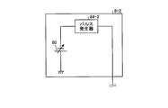
- FIG. 1 is a diagram illustrating a configuration example of the substrate processing apparatus according to the first embodiment.
- FIG. 2 is a diagram illustrating a configuration example of the power supply unit according to the first embodiment.
- FIG. 3 is a diagram showing an example of an ideal DC pulse voltage waveform according to the first embodiment.
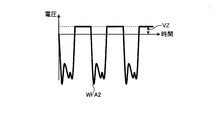
- FIG. 4 is a diagram showing an example of an actual DC pulse voltage waveform according to the first embodiment.
- FIG. 5 is a diagram illustrating a configuration example of the power supply unit according to the second embodiment.
- FIG. 6 is a diagram showing an example of an ideal DC pulse voltage waveform according to the second embodiment.
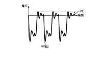
- FIG. 7 is a diagram showing an example of an actual DC pulse voltage waveform according to the second embodiment.
- FIG. 8 is a diagram illustrating a configuration example of the substrate processing apparatus according to the third embodiment.
- FIG. 9 is a diagram illustrating an example of voltage limitation according to the third embodiment.
- FIG. 10 is a diagram illustrating an example of voltage limitation according to the third embodiment.
- FIG. 11 is a diagram illustrating a configuration example of the substrate processing apparatus according to the fourth embodiment.
- FIG. 12 is a diagram illustrating a configuration example of the voltage controller according to the fourth embodiment.
- FIG. 13 is a diagram illustrating a configuration example of the voltage controller according to the fourth embodiment.
- FIG. 14 is a diagram illustrating a configuration example of the voltage controller according to the fourth embodiment.
- FIG. 15 is a diagram showing a configuration example of the substrate processing apparatus according to the fifth embodiment.
- FIG. 16 is a diagram illustrating an example of waveform shaping according to the fifth embodiment.
- FIG. 17 is a diagram illustrating an example of waveform shaping according to the fifth embodiment.
- FIG. 18 is a diagram illustrating an example of waveform shaping according to the fifth embodiment.
- FIG. 19 is a diagram illustrating an example of waveform shaping according to the fifth embodiment.
- FIG. 20 is a diagram illustrating an example of waveform shaping according to the fifth embodiment.
- FIG. 21 is a diagram showing a configuration example of the substrate processing apparatus according to the sixth embodiment.
- FIG. 1 is a diagram illustrating a configuration example of the substrate processing apparatus according to the first embodiment.
- the substrate processing apparatus 1 shown in FIG. 1 is configured as a capacitively coupled parallel plate substrate processing apparatus.
- the substrate processing apparatus 1 has a chamber 10 which is a metal processing container made of, for example, aluminum or stainless steel.
- the chamber 10 is grounded for safety.
- a disk-shaped susceptor 12 is horizontally arranged in the chamber 10. On the susceptor 12, a semiconductor wafer W as a substrate to be processed for substrate processing can be placed. The susceptor 12 also functions as a lower electrode. A gate valve 28 that opens and closes a loading/unloading port for the semiconductor wafer W is attached to a sidewall of the chamber 10.
- the susceptor 12 is made of, for example, AlN ceramic or the like, and is supported by an insulating cylindrical support portion 14 extending vertically upward from the bottom of the chamber 10.
- An annular exhaust passage 18 is formed between the side wall of the chamber 10 and a conductive cylindrical support portion (inner wall portion) 16 extending vertically upward from the bottom of the chamber 10 along the outer periphery of the cylindrical support portion 14. There is. An exhaust port 22 is provided at the bottom of the exhaust passage 18.
- An exhaust device 26 is connected to the exhaust port 22 via an exhaust pipe 24.
- the exhaust device 26 has a vacuum pump such as a turbo molecular pump, and reduces the processing space PS in the chamber 10 to a desired vacuum degree.
- the inside of the chamber 10 is preferably maintained at a constant pressure in the range of, for example, 10 mTorr to 3500 mTorr.
- the susceptor 12 used as the lower electrode is grounded via the connecting rod 36.
- a semiconductor wafer W to be processed is placed on the susceptor 12, and an edge ring 38 is provided so as to surround the semiconductor wafer W.
- the edge ring 38 is made of a conductive material (for example, Ni, Al, etc.) and is detachably attached to the upper surface of the susceptor 12.
- An electrostatic chuck 40 for attracting a wafer is provided on the upper surface of the susceptor 12.
- the electrostatic chuck 40 is formed by sandwiching a sheet-shaped or mesh-shaped conductor between film-shaped or plate-shaped dielectrics.
- a DC power source 42 arranged outside the chamber 10 is electrically connected to a conductor inside the electrostatic chuck 40 via an ON/OFF switch 44 and a power supply line 46.
- the semiconductor wafer W is attracted and held on the electrostatic chuck 40 by the Coulomb force generated in the electrostatic chuck 40 by the DC voltage applied from the DC power source 42 to the electrostatic chuck 40.
- an annular coolant chamber 48 extending in the circumferential direction is provided inside the susceptor 12.
- a coolant for example, cooling water
- a chiller unit (not shown)
- the temperature of the semiconductor wafer W on the electrostatic chuck 40 is controlled.
- the heat transfer gas for example, He gas
- the heat transfer gas supply unit is passed through the gas supply pipe 51 and the gas passage 56 in the susceptor 12. And is supplied between the electrostatic chuck 40 and the semiconductor wafer W.
- a disk-shaped inner upper electrode 60 and a ring-shaped outer upper electrode 62 are concentrically provided on the ceiling of the chamber 10 so as to face (that is, face each other) in parallel with the susceptor 12.
- the inner upper electrode 60 has a diameter (diameter) similar to that of the semiconductor wafer W
- the outer upper electrode 62 has a diameter (inner diameter/outer diameter) similar to that of the edge ring 38. ing.
- the inner upper electrode 60 and the outer upper electrode 62 are electrically insulated from each other.
- a ring-shaped insulator 63 made of, for example, ceramic is inserted between the electrodes 60 and 62.
- the inner upper electrode 60 has an electrode plate 64 that faces the susceptor 12 directly in front, and an electrode support 66 that detachably supports the electrode plate 64 from behind (above) it.
- a material for the electrode plate 64 a conductive material such as Ni or Al is preferable.
- the electrode support 66 is made of, for example, alumite-treated aluminum.
- the outer upper electrode 62 also has an electrode plate 68 that faces the susceptor 12, and an electrode support 70 that detachably supports the electrode plate 68 from behind (above) it.
- the electrode plate 68 and the electrode support member 70 are preferably made of the same material as the electrode plate 64 and the electrode support member 66, respectively.
- the inner upper electrode 60 and the outer upper electrode 62 may be collectively referred to as "upper electrodes 60, 62".
- the disk-shaped susceptor 12 that is, the lower electrode
- the disk-shaped upper electrodes 60 and 62 are arranged in parallel to each other and face each other.
- the case where the upper electrodes 60 and 62 are composed of two members, that is, the inner upper electrode 60 and the outer upper electrode 62 has been described as an example.
- the upper electrode may be composed of one member.
- the gas supply unit 76 supplies a film forming raw material gas to the chamber 10 as a processing gas.
- the inner upper electrode 60 is also used as a shower head in order to supply the film forming raw material gas to the processing space PS set between the upper electrodes 60 and 62 and the susceptor 12.
- the gas diffusion chamber 72 is provided inside the electrode support 66, and a large number of gas ejection holes 74 penetrating from the gas diffusion chamber 72 to the susceptor 12 side are formed in the electrode support 66 and the electrode plate 64.
- a gas supply pipe 78 extending from the gas supply unit 76 is connected to the gas introduction port 72 a provided in the upper portion of the gas diffusion chamber 72.
- the shower head may be provided not only on the inner upper electrode 60 but also on the outer upper electrode 62.
- a power supply unit 8 is arranged outside the chamber 10.
- the power supply unit 8 is connected to the upper electrodes 60 and 62 via a power supply line 88 and applies a DC pulse voltage to the upper electrodes 60 and 62.
- a ring-shaped ground part 96 made of a conductive material such as Ni or Al is attached to an appropriate portion of the chamber 10 facing the processing space PS (for example, the outer side of the outer upper electrode 62 in the radial direction). ..
- the ground part 96 is attached to a ring-shaped insulator 98 made of, for example, ceramic, connected to the ceiling wall of the chamber 10, and grounded via the chamber 10.
- control unit The individual operation of each component in the substrate processing apparatus 1 and the overall operation (sequence) of the substrate processing apparatus 1 are controlled by a control unit (not shown).
- control unit the operations of the exhaust device 26, the on/off switch 44, the gas supply unit 76, the chiller unit (not shown), the heat transfer gas supply unit (not shown), etc. are controlled by the control unit (not shown).
- a microcomputer is an example of the control unit.
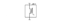
- FIG. 2 is a diagram illustrating a configuration example of the power supply unit according to the first embodiment.
- the power supply unit 8-1 shown in FIG. 2 corresponds to the power supply unit 8 shown in FIG. In FIG. 2, the power supply unit 8-1 has variable DC power supplies 81-1 and 81-2 and a pulse generator 84-1.
- the output terminal of the variable DC power supply 81-1 is connected to the pulse generator 84-1 and the variable DC power supply 81-1 outputs a negative DC voltage (that is, a negative DC voltage) to the pulse generator 84-1.
- the output terminal of the variable DC power supply 81-2 is connected to the pulse generator 84-1, and the variable DC power supply 81-2 outputs a positive DC voltage (that is, a positive DC voltage) to the pulse generator 84-1.
- the pulse generator 84-1 uses a negative DC voltage input from the variable DC power supply 81-1 and a positive DC voltage input from the variable DC power supply 81-2 to generate a DC pulse voltage (that is, a DC pulse voltage).
- the frequency of the DC pulse voltage generated by the pulse generator 84-1 is preferably 10 kHz to 1 MHz, for example.
- the duty ratio of the DC pulse voltage generated by the pulse generator 84-1 is preferably 5% to 95%.
- FIG. 3 is a diagram showing an example of an ideal DC pulse voltage waveform according to the first embodiment.
- V11 negative voltage
- V12 positive voltage
- VC1 positive steady voltage
- WFA1 A DC pulse voltage of a rectangular wave WFA1 having the following is output.
- FIG. 4 is a diagram showing an example of an actual DC pulse voltage waveform according to the first embodiment. That is, the DC pulse voltage having the waveform WFA2 has the overshoot OS11 that exceeds the steady voltage VC1. In particular, when the inductance of the discharge path in the chamber 10 is large, the overshoot OS11 occurs.
- the negative voltage is applied to the upper electrodes 60 and 62 in the periods I11, I13, and I15, and the positive voltage having the overshoot OS11 is generated in the periods I12, I14, and I16. It is applied to the upper electrodes 60 and 62. That is, the pulse generator 84-1 uses the negative DC voltage input from the variable DC power supply 81-1 and the positive DC voltage input from the variable DC power supply 81-2 to generate the DC pulse voltage of the waveform WFA2. By outputting, both positive and negative voltages are applied to the upper electrodes 60 and 62.
- the pulse generator 84-1 outputs the DC pulse voltage of the waveform WFA2, whereby the radical density control and the ion energy control can be alternately performed in time series. That is, it becomes possible to control both the radical density and the ion energy with the single power supply unit 8-1.
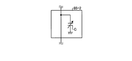
- FIG. 5 is a diagram illustrating a configuration example of the power supply unit according to the second embodiment.
- the power supply unit 8-2 shown in FIG. 5 corresponds to the power supply unit 8 shown in FIG.
- the power supply unit 8-2 has a variable DC power supply 80 and a pulse generator 84-2.
- the output terminal of the variable DC power supply 80 is connected to the pulse generator 84-2, and the variable DC power supply 80 outputs a negative DC voltage to the pulse generator 84-2.
- the pulse generator 84-2 uses the negative DC voltage input from the variable DC power supply 80 to generate a DC pulse voltage, and supplies the generated DC pulse voltage to the upper electrodes 60 and 62 via the power supply line 88. To do.
- the frequency of the DC pulse voltage generated by the pulse generator 84-2 is preferably 10 kHz to 1 MHz, for example.
- the duty ratio of the DC pulse voltage generated by the pulse generator 84-2 is preferably 5% to 95%.
- FIG. 6 is a diagram showing an example of an ideal DC pulse voltage waveform according to the second embodiment.
- FIG. 7 is a diagram showing an example of an actual DC pulse voltage waveform according to the second embodiment. That is, the DC pulse voltage having the waveform WFB2 has the overshoot OS21 that exceeds the steady voltage VC2. In particular, when the inductance of the discharge path in the chamber 10 is large, the overshoot OS21 occurs.
- the pulse generator 84-2 outputs the DC pulse voltage of the waveform WFB2 using the negative DC voltage input from the variable DC power supply 80, so that both positive and negative voltages are applied to the upper electrodes 60 and 62. ..
- the pulse generator 84-2 outputs the DC pulse voltage of the waveform WFB2, whereby the radical density control and the ion energy control can be alternately performed in time series. That is, both the radical density and the ion energy can be controlled by the single power supply unit 8-2.
- the substrate processing apparatus 1 includes the chamber 10 that can be evacuated, the susceptor 12 used as the lower electrode, the upper electrodes 60 and 62, and the power supply unit 8.
- a substrate to be processed is placed on the susceptor 12.
- the upper electrodes 60 and 62 are arranged inside the chamber 10 so as to face the susceptor 12.
- the power supply unit 8 applies a DC pulse voltage to the upper electrodes 60 and 62.
- the substrate processing apparatus 1 does not have a power supply unit that applies an AC voltage to the upper electrodes 60 and 62, a power supply unit that applies an AC voltage to the susceptor 12, and a power supply unit that applies a DC voltage to the susceptor 12.
- the power supply unit 8-1 includes a variable DC power supply 81-1 that outputs a negative DC voltage, a variable DC power supply 81-2 that outputs a positive DC voltage, and a pulse generator 84-1.
- the pulse generator 84-1 generates a DC pulse voltage using the negative DC voltage output from the variable DC power supply 81-1 and the positive DC voltage output from the variable DC power supply 81-2.
- the power supply unit 8-2 has the variable DC power supply 80 that outputs a negative DC voltage and the pulse generator 84-2.
- the pulse generator 84-2 uses the negative DC voltage output from the variable DC power supply 80 to generate a DC pulse voltage.
- the substrate processing apparatus 1 does not have a power supply unit other than the power supply unit 8 and can apply both positive and negative voltages to the upper electrodes 60 and 62 with only the single power supply unit 8. Therefore, both the radical density and the ion energy can be controlled without using a power supply unit other than the power supply unit 8. Therefore, the scale of the substrate processing apparatus 1 can be reduced.
- FIG. 8 is a diagram illustrating a configuration example of the substrate processing apparatus according to the third embodiment.
- the substrate processing apparatus 2 (FIG. 8) according to the third embodiment is different from the substrate processing apparatus 1 (FIG. 1) according to the first embodiment in that it has a voltage limiter 82.
- the voltage limiter 82 limits the maximum value of the positive voltage in the DC pulse voltage output from the power supply unit 8.
- the voltage limiter 82 is realized by using, for example, a Zener diode.
- the voltage limiter 82 sets the maximum value of the positive voltage in the DC pulse voltage having the waveform WFA2 as shown in FIG. Limit to the voltage value VZ.
- the voltage limiter 82 has the maximum value of the positive voltage in the DC pulse voltage having the waveform WFB2 as shown in FIG. Is limited to the voltage value VZ.
- 9 and 10 are diagrams showing an example of voltage limitation according to the third embodiment.
- the potential difference between the upper electrodes 60 and 62 and the susceptor 12 is different from the first and second embodiments. Can be extended for a long period. By making the period during which the potential difference between the upper electrodes 60 and 62 and the susceptor 12 is constant longer than that in the first embodiment, the width of the ion energy distribution can be made narrower than that in the first embodiment.
- FIG. 11 is a diagram illustrating a configuration example of the substrate processing apparatus according to the fourth embodiment.
- the substrate processing apparatus 3 (FIG. 11) according to the fourth embodiment is different from the substrate processing apparatus 1 (FIG. 1) according to the first embodiment in that it has a voltage controller 85.
- the voltage controller 85 controls the magnitude of the positive voltage in the DC pulse voltage output from the power supply unit 8.
- FIG 12, 13, and 14 are diagrams showing a configuration example of the voltage controller according to the fourth embodiment.
- the voltage controller 85 has the configuration shown in FIG.
- the voltage controller 85-1 shown in FIG. 12 corresponds to the voltage controller 85 shown in FIG.
- the voltage controller 85-1 is formed by the variable coil L connected in series between the power supply unit 8 and the upper electrodes 60 and 62. As the inductance of the variable coil L is increased, the magnitude of the positive voltage in the DC pulse voltage is increased and the ion energy can be increased.
- the voltage controller 85 has the configuration shown in FIG.
- the voltage controller 85-2 shown in FIG. 13 corresponds to the voltage controller 85 shown in FIG.
- the voltage controller 85-2 is formed by the variable capacitor C connected in parallel between the upper electrodes 60 and 62 and the ground. As the capacitance of the variable capacitor C is reduced, the magnitude of the positive voltage in the DC pulse voltage is increased, and the ion energy can be increased.
- the voltage controller 85 has the configuration shown in FIG.
- the voltage controller 85-3 shown in FIG. 14 corresponds to the voltage controller 85 shown in FIG.
- the voltage controller 85-3 is formed by a variable resistor R connected in series between the power supply unit 8 and the upper electrodes 60 and 62. The smaller the resistance value of the variable resistor R, the larger the magnitude of the positive voltage in the DC pulse voltage, and the more the ion energy can be increased.
- the voltage controller 85 is formed by using the variable coil L, the variable capacitor C, or the variable resistor R, but the voltage controller 85 is formed by using a non-variable coil, capacitor, or resistor. 85 may be formed.
- the amount of ion energy can be controlled by controlling the magnitude of the positive voltage in the DC pulse voltage.
- the fourth embodiment has been described above.
- FIG. 15 is a diagram showing a configuration example of the substrate processing apparatus according to the fifth embodiment.
- the substrate processing apparatus 4 (FIG. 15) according to the fifth embodiment is different from the substrate processing apparatus 1 (FIG. 1) according to the first embodiment in that a waveform shaping device 83 is included.
- the waveform shaper 83 shapes the waveform of the DC pulse voltage output from the power supply unit 8.
- 16 to 20 are diagrams showing an example of waveform shaping according to the fifth embodiment.
- the waveform shaper 83 shapes the waveform of the DC pulse voltage output from the power supply unit 8 into a sine wave WF01 as shown in the left diagram of FIG.
- the maximum and minimum values of the DC pulse voltage that is, the maximum and minimum values of the sine wave WF01
- the waveform shaper 83 shapes the waveform of the DC pulse voltage output from the power supply unit 8 into a triangular wave WF02, as shown in FIG.
- the waveform shaper 83 shapes the waveform of the DC pulse voltage output from the power supply unit 8 into a triangular wave WF02, as shown in FIG.
- the waveform shaper 83 shapes the waveform of the DC pulse voltage output from the power supply unit 8 into a rectangular wave WF03, as shown in FIG.
- the waveform shaper 83 shapes the waveform of the DC pulse voltage output from the power supply unit 8 into a rectangular wave WF03, as shown in FIG.
- the substrate processing apparatus 4 since the substrate processing apparatus 4 has the waveform shaping device 83, it is possible to obtain the ion energy distribution according to the waveform after shaping.
- the fifth embodiment has been described above.
- FIG. 21 is a diagram showing a configuration example of the substrate processing apparatus according to the sixth embodiment.
- the substrate processing apparatus 5 (FIG. 21) according to the sixth embodiment is different from the substrate processing apparatus 1 (FIG. 1) according to the first embodiment in that the susceptor 12 is not grounded and is floating.
- the susceptor 12 is grounded by connecting the connector 86-1 and the connector 86-2. On the other hand, by separating the connector 86-1 and the connector 86-2, the susceptor 12 is floated without being grounded.
- the susceptor 12 is floated without being grounded, so that the potential of the susceptor 12 easily follows the potentials of the upper electrodes 60 and 62. Therefore, the potential difference between the upper electrodes 60 and 62 and the susceptor 12 becomes small, so that the acceleration voltage of ions becomes small. Therefore, the ion energy can be reduced by floating the susceptor 12 without being grounded.
- the embodiments of the present disclosure are illustrative in all points and not restrictive. Indeed, the above embodiments may be implemented in various forms. Further, the above-described embodiment may be omitted, replaced, or modified in various forms without departing from the scope and spirit of the claims.
- film formation has been described as an example of substrate processing in the above description, the substrate processing to which the technique of the present disclosure is applicable is not limited to film formation.
- the technique of the present disclosure can be applied to etching, which is one of substrate processing.
Landscapes
- Chemical & Material Sciences (AREA)
- Physics & Mathematics (AREA)
- Engineering & Computer Science (AREA)
- Plasma & Fusion (AREA)
- General Chemical & Material Sciences (AREA)
- Spectroscopy & Molecular Physics (AREA)
- Electromagnetism (AREA)
- Chemical Kinetics & Catalysis (AREA)
- Materials Engineering (AREA)
- Mechanical Engineering (AREA)
- Metallurgy (AREA)
- Organic Chemistry (AREA)
- Plasma Technology (AREA)
- Drying Of Semiconductors (AREA)
- Chemical Vapour Deposition (AREA)
Abstract
本開示の基板処理装置は、真空排気可能な処理容器と、下部電極と、上部電極と、電源ユニットとを有する。下部電極には被処理基板を載置可能である。上部電極は、処理容器内で下部電極に対向して配置される。電源ユニットは、直流パルス電圧を上部電極に印加する。一方で、本開示の基板処理装置は、交流電圧を上部電極に印加する電源ユニット、交流電圧を下部電極に印加する電源ユニット、及び、直流電圧を下部電極に印加する電源ユニットを有しない。
Description
本開示は、基板処理装置及び基板処理方法に関する。
半導体集積回路の製造では、基板処理装置によって、半導体ウエハ等の基板に対する処理(以下では「基板処理」と呼ぶことがある)が行われる。基板処理装置では、基板処理として、例えば、所定の真空度にされたチャンバ(処理容器)内に基板が配置され、チャンバ内に成膜原料ガスが供給されてプラズマが生成されることにより、基板に対して成膜が行われる。
上記のようなプラズマを用いた成膜では、ラジカル密度及びイオンエネルギが膜質に影響を与える。これに対し、従来の基板処理装置では、チャンバの上部電極に比較的高周波の交流電源が接続されてプラズマの生成が行われる一方で、基板が存在する下部電極に比較的低周波の交流電源または直流電源が接続されてイオンの引き込み(つまり、上部電極から下部電極へのイオンの加速)が行われている。このため、従来の基板処理装置には、ラジカル密度及びイオンエネルギの各々を制御するために、比較的高周波の交流電源を有する電源ユニット、及び、比較的低周波の交流電源または直流電源を有する電源ユニットの2つの電源ユニットが備えられている。このように、従来の基板処理装置には少なくとも2つの電源ユニットが備えられているため、基板処理装置の装置規模が大きくなっていた。
本開示は、基板処理装置の装置規模を小さくすることができる技術を提供する。
本開示の一態様の基板処理装置は、真空排気可能な処理容器と、下部電極と、上部電極と、電源ユニットとを有する。下部電極には被処理基板を載置可能である。上部電極は、処理容器内で下部電極に対向して配置される。電源ユニットは、直流パルス電圧を上部電極に印加する。一方で、本開示の一態様の基板処理装置は、交流電圧を上部電極に印加する電源ユニット、交流電圧を下部電極に印加する電源ユニット、及び、直流電圧を下部電極に印加する電源ユニットを有しない。
本開示の技術によれば、基板処理装置の装置規模を小さくすることができる。
以下に、本開示の技術の実施形態を図面に基づいて説明する。各実施形態において同一の構成には同一の符号を付すことにより、実施形態間で重複する説明は省略する。
[実施形態1]
<基板処理装置の構成>
図1は、実施形態1に係る基板処理装置の構成例を示す図である。図1に示す基板処理装置1は、容量結合型の平行平板基板処理装置として構成されている。
<基板処理装置の構成>
図1は、実施形態1に係る基板処理装置の構成例を示す図である。図1に示す基板処理装置1は、容量結合型の平行平板基板処理装置として構成されている。
図1において、基板処理装置1は、例えばアルミニウムまたはステンレス鋼等からなる金属製の処理容器であるチャンバ10を有する。チャンバ10は保安接地されている。
チャンバ10内には、円盤状のサセプタ12が水平に配置されている。サセプタ12には、基板処理の被処理基板としての半導体ウエハWを載置可能である。サセプタ12は、下部電極としても機能する。チャンバ10の側壁には、半導体ウエハWの搬入出口を開閉するゲートバルブ28が取り付けられている。サセプタ12は、例えばAlNセラミック等からなり、チャンバ10の底から鉛直上方に延びる絶縁性の筒状支持部14に支持されている。
筒状支持部14の外周に沿ってチャンバ10の底から鉛直上方に延びる導電性の筒状支持部(内壁部)16とチャンバ10の側壁との間に、環状の排気路18が形成されている。排気路18の底には排気口22が設けられている。
排気口22には排気管24を介して排気装置26が接続されている。排気装置26は、例えばターボ分子ポンプ等の真空ポンプを有しており、チャンバ10内の処理空間PSを所望の真空度まで減圧する。チャンバ10内は、例えば、10mTorr~3500mTorrの範囲の一定の圧力に保たれるのが好ましい。
下部電極として用いられるサセプタ12は、接続棒36を介して接地されている。
サセプタ12の上には基板処理対象の半導体ウエハWが載置され、半導体ウエハWを囲むようにエッジリング38が設けられている。エッジリング38は、導電材(例えばNi,Al等)からなり、サセプタ12の上面に着脱可能に取り付けられる。
また、サセプタ12の上面には、ウエハ吸着用の静電チャック40が設けられている。静電チャック40は、膜状または板状の誘電体の間にシート状またはメッシュ状の導電体を挟んで形成される。静電チャック40内の導電体には、チャンバ10の外に配置される直流電源42がオン/オフ切替スイッチ44及び給電線46を介して電気的に接続されている。直流電源42より静電チャック40へ印加される直流電圧によって静電チャック40に発生するクーロン力により、半導体ウエハWが静電チャック40上に吸着保持される。
サセプタ12の内部には、円周方向に延びる環状の冷媒室48が設けられている。冷媒室48には、チラーユニット(図示せず)より配管50,52を介して、所定温度の冷媒(例えば冷却水)が循環供給される。冷媒の温度を制御することによって静電チャック40上の半導体ウエハWの温度が制御される。さらに、半導体ウエハWの温度の精度を高めるために、伝熱ガス供給部(図示せず)からの伝熱ガス(例えばHeガス)が、ガス供給管51及びサセプタ12内のガス通路56を介して、静電チャック40と半導体ウエハWとの間に供給される。
チャンバ10の天井には、サセプタ12と平行に向かい合って(つまり、対向して)、円盤状の内側上部電極60及びリング状の外側上部電極62が同心状に設けられている。径方向の好適なサイズとして、内側上部電極60は半導体ウエハWと同程度の口径(直径)を有し、外側上部電極62はエッジリング38と同程度の口径(内径・外径)を有している。内側上部電極60と外側上部電極62とは互いに電気的に絶縁されている。両電極60,62の間には、例えばセラミックからなるリング状の絶縁体63が挿入されている。
内側上部電極60は、サセプタ12と真正面に向かい合う電極板64と、電極板64をその背後(上)から着脱可能に支持する電極支持体66とを有している。電極板64の材質として、NiまたはAl等の導電材が好ましい。電極支持体66は、例えばアルマイト処理されたアルミニウムで構成される。外側上部電極62も、サセプタ12と向かい合う電極板68と、電極板68をその背後(上)から着脱可能に支持する電極支持体70とを有している。電極板68及び電極支持体70は、電極板64及び電極支持体66とそれぞれ同じ材質で構成されるのが好ましい。以下では、内側上部電極60と外側上部電極62とを「上部電極60,62」と総称することがある。このように、基板処理装置1では、円盤状のサセプタ12(つまり、下部電極)と、円盤状の上部電極60,62とが互いに平行に対向して配置されている。
なお、本実施形態では、上部電極60,62が、内側上部電極60と外側上部電極62との2つの部材で構成される場合を一例として挙げた。しかし、上部電極は1つの部材で構成されても良い。
ガス供給部76は、処理ガスとして、チャンバ10に成膜原料ガスを供給する。上部電極60,62とサセプタ12との間に設定される処理空間PSに成膜原料ガスを供給するために、内側上部電極60がシャワーヘッドとして兼用される。より詳細には、電極支持体66の内部にガス拡散室72が設けられ、ガス拡散室72からサセプタ12側に貫ける多数のガス吐出孔74が電極支持体66及び電極板64に形成される。ガス拡散室72の上部に設けられるガス導入口72aには、ガス供給部76から延びるガス供給管78が接続されている。なお、内側上部電極60だけでなく外側上部電極62にもシャワーヘッドを設ける構成としても良い。
チャンバ10の外には、電源ユニット8が配置されている。電源ユニット8は、給電ライン88を介して上部電極60,62に接続され、直流パルス電圧を上部電極60,62に印加する。
チャンバ10内で処理空間PSに面する適当な箇所(例えば、外側上部電極62の半径方向外側)には、例えばNi,Al等の導電性部材からなるリング状のグランドパーツ96が取り付けられている。グランドパーツ96は、例えばセラミックからなるリング状の絶縁体98に取り付けられるとともに、チャンバ10の天井壁に接続されており、チャンバ10を介して接地されている。プラズマ処理中に上部電極60,62に電圧が印加されると、プラズマを介して上部電極60,62とグランドパーツ96との間で電子電流が流れる。
基板処理装置1内の各構成の個々の動作、及び、基板処理装置1全体の動作(シーケンス)は、制御部(図示せず)によって制御される。例えば、排気装置26、オン/オフ切替スイッチ44、ガス供給部76、チラーユニット(図示せず)、伝熱ガス供給部(図示せず)等の動作は、制御部(図示せず)によって制御される。制御部の一例として、マイクロコンピュータが挙げられる。
<電源ユニットの構成>
図2は、実施形態1に係る電源ユニットの構成例を示す図である。図2に示す電源ユニット8-1は、図1に示す電源ユニット8に該当する。図2において、電源ユニット8-1は、可変直流電源81-1,81-2と、パルス発生器84-1とを有する。
図2は、実施形態1に係る電源ユニットの構成例を示す図である。図2に示す電源ユニット8-1は、図1に示す電源ユニット8に該当する。図2において、電源ユニット8-1は、可変直流電源81-1,81-2と、パルス発生器84-1とを有する。
可変直流電源81-1の出力端子はパルス発生器84-1に接続され、可変直流電源81-1は、負の直流電圧(つまり負のDC電圧)をパルス発生器84-1に出力する。また、可変直流電源81-2の出力端子はパルス発生器84-1に接続され、可変直流電源81-2は、正の直流電圧(つまり正のDC電圧)をパルス発生器84-1に出力する。パルス発生器84-1は、可変直流電源81-1から入力される負の直流電圧と、可変直流電源81-2から入力される正の直流電圧とを用いて、直流パルス電圧(つまりDCパルス電圧)を発生し、発生した直流パルス電圧を給電ライン88を介して上部電極60,62に供給する。パルス発生器84-1が発生する直流パルス電圧の周波数は、例えば、10kHz~1MHzであることが好ましい。また、パルス発生器84-1が発生する直流パルス電圧のデューティ比は、5%~95%であることが好ましい。
図3は、実施形態1に係る理想的な直流パルス電圧波形の一例を示す図である。チャンバ10での放電経路の電気的特性が理想的な状態にあるときは、パルス発生器84-1からは、負電圧V11と、正電圧V12と、正の定常電圧VC1(VC1=V12)とを有する矩形波WFA1の直流パルス電圧が出力される。
しかし、一般的に、チャンバ10での放電経路の電気的特性は理想的な状態にないため、パルス発生器84-1から出力される直流パルス電圧は、実際には、図4に示す波形WFA2を有する電圧となる。図4は、実施形態1に係る実際の直流パルス電圧波形の一例を示す図である。すなわち、波形WFA2を有する直流パルス電圧には、定常電圧VC1を超過したオーバーシュートOS11が生じる。特に、チャンバ10での放電経路のインダクタンスが大きい場合に、オーバーシュートOS11が生じる。
このように、実際の直流パルス電圧は波形WFA2を有するため、期間I11,I13,I15では負電圧が上部電極60,62に印加され、期間I12,I14,I16ではオーバーシュートOS11を有する正電圧が上部電極60,62に印加される。つまり、パルス発生器84-1が、可変直流電源81-1から入力される負の直流電圧と、可変直流電源81-2から入力される正の直流電圧とを用いて波形WFA2の直流パルス電圧を出力することにより、正負両電圧が上部電極60,62に印加される。
期間I11,I13,I15では、負電圧が上部電極60,62に印加されるため、チャンバ10内でプラズマが生成され、生成されたプラズマが維持される。負電圧の大きさの絶対値が大きいほど、プラズマの生成量は大きくなる。一方で、期間I12,I14,I16では、正電圧が上部電極60,62に印加されるため、チャンバ10内でイオンがZ方向(図1)に加速される。正電圧の大きさが大きいほど、イオンの加速量は大きくなる。よって、パルス発生器84-1が波形WFA2の直流パルス電圧を出力することで、ラジカル密度の制御と、イオンエネルギの制御とを、時系列で交互に行うことができる。つまり、単一の電源ユニット8-1によって、ラジカル密度及びイオンエネルギの双方を制御することが可能になる。
以上、実施形態1について説明した。
[実施形態2]
実施形態2では、電源ユニット8の構成が実施形態1と異なる。
実施形態2では、電源ユニット8の構成が実施形態1と異なる。
<電源ユニットの構成>
図5は、実施形態2に係る電源ユニットの構成例を示す図である。図5に示す電源ユニット8-2は、図1に示す電源ユニット8に該当する。図5において、電源ユニット8-2は、可変直流電源80と、パルス発生器84-2とを有する。
図5は、実施形態2に係る電源ユニットの構成例を示す図である。図5に示す電源ユニット8-2は、図1に示す電源ユニット8に該当する。図5において、電源ユニット8-2は、可変直流電源80と、パルス発生器84-2とを有する。
可変直流電源80の出力端子はパルス発生器84-2に接続され、可変直流電源80は、負の直流電圧をパルス発生器84-2に出力する。パルス発生器84-2は、可変直流電源80から入力される負の直流電圧を用いて、直流パルス電圧を発生し、発生した直流パルス電圧を給電ライン88を介して上部電極60,62に供給する。パルス発生器84-2が発生する直流パルス電圧の周波数は、例えば、10kHz~1MHzであることが好ましい。また、パルス発生器84-2が発生する直流パルス電圧のデューティ比は、5%~95%であることが好ましい。
図6は、実施形態2に係る理想的な直流パルス電圧波形の一例を示す図である。チャンバ10での放電経路の電気的特性が理想的な状態にあるときは、パルス発生器84-2からは、負電圧V21と、定常電圧VC2(VC2=0V)とを有する矩形波WFB1の直流パルス電圧が出力される。
しかし、一般的に、チャンバ10での放電経路の電気的特性は理想的な状態にないため、パルス発生器84-2から出力される直流パルス電圧は、実際には、図7に示す波形WFB2を有する電圧となる。図7は、実施形態2に係る実際の直流パルス電圧波形の一例を示す図である。すなわち、波形WFB2を有する直流パルス電圧には、定常電圧VC2を超過したオーバーシュートOS21が生じる。特に、チャンバ10での放電経路のインダクタンスが大きい場合に、オーバーシュートOS21が生じる。
このように、実際の直流パルス電圧は波形WFB2を有するため、期間I21,I23,I25では負電圧が上部電極60,62に印加され、期間I22,I24,I26ではオーバーシュートOS21を有する正電圧が上部電極60,62に印加される。つまり、パルス発生器84-2が、可変直流電源80から入力される負の直流電圧を用いて波形WFB2の直流パルス電圧を出力することにより、正負両電圧が上部電極60,62に印加される。
期間I21,I23,I25では、負電圧が上部電極60,62に印加されるため、チャンバ10内でプラズマが生成され、生成されたプラズマが維持される。負電圧の大きさの絶対値が大きいほど、プラズマの生成量は大きくなる。一方で、期間I22,I24,I26では、正電圧が上部電極60,62に印加されるため、チャンバ10内でイオンがZ方向に加速される。オーバーシュートOS21の大きさ(つまり、正電圧の大きさ)が大きいほど、イオンの加速量は大きくなる。よって、パルス発生器84-2が波形WFB2の直流パルス電圧を出力することで、ラジカル密度の制御と、イオンエネルギの制御とを、時系列で交互に行うことができる。つまり、単一の電源ユニット8-2によって、ラジカル密度及びイオンエネルギの双方を制御することが可能になる。
以上、実施形態2について説明した。
以上のように、実施形態1,2では、基板処理装置1は、真空排気可能なチャンバ10と、下部電極として用いられるサセプタ12、上部電極60,62と、電源ユニット8とを有する。サセプタ12には被処理基板が載置される。上部電極60,62は、チャンバ10内でサセプタ12に対向して配置される。電源ユニット8は、直流パルス電圧を上部電極60,62に印加する。一方で、基板処理装置1は、交流電圧を上部電極60,62に印加する電源ユニット、交流電圧をサセプタ12に印加する電源ユニット、及び、直流電圧をサセプタ12に印加する電源ユニットを有しない。
例えば、実施形態1では、電源ユニット8-1は、負の直流電圧を出力する可変直流電源81-1と、正の直流電圧を出力する可変直流電源81-2と、パルス発生器84-1とを有する。パルス発生器84-1は、可変直流電源81-1から出力される負の直流電圧と、可変直流電源81-2から出力される正の直流電圧とを用いて、直流パルス電圧を発生する。
また例えば、実施形態2では、電源ユニット8-2は、負の直流電圧を出力する可変直流電源80と、パルス発生器84-2とを有する。パルス発生器84-2は、可変直流電源80から出力される負の直流電圧を用いて、直流パルス電圧を発生する。
こうすることで、基板処理装置1は、電源ユニット8以外の電源ユニットを有さずに、単一の電源ユニット8だけで、正負両電圧を上部電極60,62に印加することができる。このため、電源ユニット8以外の電源ユニットを用いずに、ラジカル密度及びイオンエネルギの双方を制御することが可能になる。よって、基板処理装置1の装置規模を小さくすることができる。
[実施形態3]
図8は、実施形態3に係る基板処理装置の構成例を示す図である。実施形態3に係る基板処理装置2(図8)は、実施形態1に係る基板処理装置1(図1)と比べ、電圧制限器82を有する点が異なる。
図8は、実施形態3に係る基板処理装置の構成例を示す図である。実施形態3に係る基板処理装置2(図8)は、実施形態1に係る基板処理装置1(図1)と比べ、電圧制限器82を有する点が異なる。
電圧制限器82は、電源ユニット8から出力される直流パルス電圧における正電圧の最大値を制限する。電圧制限器82は、例えばツェナーダイオードを用いて実現される。
例えば、電源ユニット8が実施形態1(図2)に記載の構成を採る場合には、電圧制限器82は、図9に示すように、波形WFA2を有する直流パルス電圧における正電圧の最大値を電圧値VZに制限する。また例えば、電源ユニット8が実施形態2(図5)に記載の構成を採る場合には、電圧制限器82は、図10に示すように、波形WFB2を有する直流パルス電圧における正電圧の最大値を電圧値VZに制限する。図9及び図10は、実施形態3に係る電圧制限の一例を示す図である。
このように、実施形態3では、直流パルス電圧における正電圧の最大値を所定の電圧値に制限することにより、実施形態1,2に比べ、上部電極60,62とサセプタ12との間の電位差が一定になる期間を長くすることができる。上部電極60,62とサセプタ12との間の電位差が一定になる期間を実施形態1よりも長くすることにより、イオンエネルギ分布の幅を実施形態1よりも狭くすることができる。
以上、実施形態3について説明した。
[実施形態4]
図11は、実施形態4に係る基板処理装置の構成例を示す図である。実施形態4に係る基板処理装置3(図11)は、実施形態1に係る基板処理装置1(図1)と比べ、電圧制御器85を有する点が異なる。
図11は、実施形態4に係る基板処理装置の構成例を示す図である。実施形態4に係る基板処理装置3(図11)は、実施形態1に係る基板処理装置1(図1)と比べ、電圧制御器85を有する点が異なる。
電圧制御器85は、電源ユニット8から出力される直流パルス電圧における正電圧の大きさを制御する。
図12,13,14は、実施形態4に係る電圧制御器の構成例を示す図である。
例えば、電圧制御器85は図12に示す構成を採る。図12に示す電圧制御器85-1は、図11に示す電圧制御器85に該当する。電圧制御器85-1は、電源ユニット8と上部電極60,62との間に直列に接続された可変コイルLにより形成される。可変コイルLのインダクタンスを大きくするほど直流パルス電圧における正電圧の大きさがより大きくなり、イオンエネルギを増加させることができる。
また例えば、電圧制御器85は図13に示す構成を採る。図13に示す電圧制御器85-2は、図11に示す電圧制御器85に該当する。電圧制御器85-2は、上部電極60,62と接地との間に並列に接続された可変コンデンサCにより形成される。可変コンデンサCの静電容量を小さくするほど直流パルス電圧における正電圧の大きさがより大きくなり、イオンエネルギを増加させることができる。
また例えば、電圧制御器85は図14に示す構成を採る。図14に示す電圧制御器85-3は、図11に示す電圧制御器85に該当する。電圧制御器85-3は、電源ユニット8と上部電極60,62との間に直列に接続された可変抵抗Rにより形成される。可変抵抗Rの抵抗値を小さくするほど直流パルス電圧における正電圧の大きさがより大きくなり、イオンエネルギを増加させることができる。
なお、図12,13,14では、可変コイルL、可変コンデンサC、または、可変抵抗Rを用いて電圧制御器85を形成したが、可変でないコイル、コンデンサ、または、抵抗を用いて電圧制御器85を形成しても良い。
このように、実施形態4では、基板処理装置3は電圧制御器85を有するため、直流パルス電圧における正電圧の大きさを制御することにより、イオンエネルギ量を制御することができる。
以上、実施形態4について説明した。
[実施形態5]
図15は、実施形態5に係る基板処理装置の構成例を示す図である。実施形態5に係る基板処理装置4(図15)は、実施形態1に係る基板処理装置1(図1)と比べ、波形成型器83を有する点が異なる。
図15は、実施形態5に係る基板処理装置の構成例を示す図である。実施形態5に係る基板処理装置4(図15)は、実施形態1に係る基板処理装置1(図1)と比べ、波形成型器83を有する点が異なる。
波形成型器83は、電源ユニット8から出力される直流パルス電圧の波形を成形する。
図16~20は、実施形態5に係る波形成形の一例を示す図である。
例えば、波形成型器83は、電源ユニット8から出力される直流パルス電圧の波形を、図16の左図に示すように、サイン波WF01に成形する。直流パルス電圧の波形がサイン波WF01に成形されることにより、直流パルス電圧の最大値及び最小値(つまり、サイン波WF01の最大値及び最小値)が上部電極60,62に印加される時間を比較的長くすることができる。よって、直流パルス電圧の波形がサイン波WF01に成形されることにより、図16の右図に示すように、低エネルギ端及び高エネルギ端の両端にピークを持つイオンエネルギ分布ED01を得ることができる。
また例えば、波形成型器83は、電源ユニット8から出力される直流パルス電圧の波形を、図17に示すように、三角波WF02に成形する。直流パルス電圧の波形が三角波WF02に成形されることにより、直流パルス電圧における各電圧が上部電極60,62に印加される時間を等しくすることができる。よって、直流パルス電圧の波形が三角波WF02に成形されることにより、図18に示すように、低エネルギから高エネルギの全体に渡って一定のイオン量となるイオンエネルギ分布ED02を得ることができる。
また例えば、波形成型器83は、電源ユニット8から出力される直流パルス電圧の波形を、図19に示すように、矩形波WF03に成形する。直流パルス電圧の波形が矩形波WF03に成形されることにより、直流パルス電圧において、上部電極60,62に印加される電圧を特定の電圧に制限することができる。よって、直流パルス電圧の波形が矩形波WF03に成形されることにより、図20に示すように、イオンエネルギが特定の値に偏ったイオンエネルギ分布ED03を得ることができる。
このように、実施形態5では、基板処理装置4は波形成型器83を有するため、成形後の波形に応じたイオンエネルギ分布を得ることができる。
以上、実施形態5について説明した。
[実施形態6]
図21は、実施形態6に係る基板処理装置の構成例を示す図である。実施形態6に係る基板処理装置5(図21)は、実施形態1に係る基板処理装置1(図1)と比べ、サセプタ12が、接地されずにフローティングされている点が異なる。
図21は、実施形態6に係る基板処理装置の構成例を示す図である。実施形態6に係る基板処理装置5(図21)は、実施形態1に係る基板処理装置1(図1)と比べ、サセプタ12が、接地されずにフローティングされている点が異なる。
図21において、コネクタ86-1とコネクタ86-2とが接続されることにより、サセプタ12が接地される。一方で、コネクタ86-1とコネクタ86-2とが分離されることにより、サセプタ12は、接地されずにフローティングされる。
このように、実施形態6では、サセプタ12が接地されずにフローティングされるため、サセプタ12の電位が上部電極60,62の電位に追従しやすくなる。このため、上部電極60,62とサセプタ12との間の電位差が小さくなるので、イオンの加速電圧が小さくなる。よって、サセプタ12が接地されずにフローティングされることにより、イオンエネルギを減少させることができる。
以上、実施形態6について説明した。
なお、本開示の実施形態はすべての点で例示であって制限的なものではないと考えられるべきである。実に、上記の実施形態は多様な形態で具現され得る。また、上記の実施形態は、特許請求の範囲及びその趣旨を逸脱することなく、様々な形態で省略、置換、変更されても良い。例えば、上記説明では基板処理の一例として成膜を挙げて説明したが、本開示の技術が適用可能な基板処理は成膜に限定されない。例えば、処理空間PSの真空度、及び、処理ガスをエッチングに適したものに変更することにより、本開示の技術を、基板処理の一つであるエッチングに適用することも可能である。
1,2,3,4,5 基板処理装置
8,8-1,8-2 電源ユニット
80,81-1,81-2 可変直流電源
10 チャンバ
12 サセプタ
60 内側上部電極
62 外側上部電極
8,8-1,8-2 電源ユニット
80,81-1,81-2 可変直流電源
10 チャンバ
12 サセプタ
60 内側上部電極
62 外側上部電極
Claims (11)
- 真空排気可能な処理容器と、
前記処理容器内で被処理基板を載置可能な下部電極と、
前記処理容器内で前記下部電極に対向して配置される上部電極と、
直流パルス電圧を前記上部電極に印加する電源ユニットと、を具備し、
交流電圧を前記上部電極に印加する電源ユニット、前記交流電圧を前記下部電極に印加する電源ユニット、及び、直流電圧を前記下部電極に印加する電源ユニットを具備しない、
基板処理装置。 - 前記電源ユニットは、負の直流電圧を出力する第一電源と、正の直流電圧を出力する第二電源と、前記負の直流電圧と前記正の直流電圧とを用いて前記直流パルス電圧を発生するパルス発生器と、を具備する、
請求項1に記載の基板処理装置。 - 前記電源ユニットは、負の直流電圧を出力する電源と、前記負の直流電圧を用いて前記直流パルス電圧を発生するパルス発生器と、を具備する、
請求項1に記載の基板処理装置。 - 前記直流パルス電圧における正電圧の最大値を制限する電圧制限器、をさらに具備する、
請求項1に記載の基板処理装置。 - 前記直流パルス電圧における正電圧の大きさを制御する電圧制御器、をさらに具備する、
請求項1に記載の基板処理装置。 - 前記電圧制御器は、前記電源ユニットと前記上部電極との間に直列に接続されたコイルにより形成される、
請求項5に記載の基板処理装置。 - 前記電圧制御器は、前記上部電極と接地との間に並列に接続されたコンデンサにより形成される、
請求項5に記載の基板処理装置。 - 前記電圧制御器は、前記電源ユニットと前記上部電極との間に直列に接続された抵抗により形成される、
請求項5に記載の基板処理装置。 - 前記直流パルス電圧の波形を成形する波形成型器、をさらに具備する、
請求項1に記載の基板処理装置。 - 前記下部電極が接地されずにフローティングされている、
請求項1に記載の基板処理装置。 - 真空排気可能な処理容器と、
前記処理容器内で被処理基板を載置可能な下部電極と、
前記処理容器内で前記下部電極に対向して配置される上部電極と、
直流パルス電圧を前記上部電極に印加する電源ユニットと、を具備する一方で、
交流電圧を前記上部電極に印加する電源ユニット、前記交流電圧を前記下部電極に印加する電源ユニット、及び、直流電圧を前記下部電極に印加する電源ユニットを具備しない基板処理装置における基板処理方法であって、
前記処理容器内に処理ガスを供給することと、
前記基板処理装置が具備する前記電源ユニットにより、前記上部電極に前記直流パルス電圧を印加することと、
を有する基板処理方法。
Applications Claiming Priority (2)
| Application Number | Priority Date | Filing Date | Title |
|---|---|---|---|
| JP2018230882A JP2020095793A (ja) | 2018-12-10 | 2018-12-10 | 基板処理装置及び基板処理方法 |
| JP2018-230882 | 2018-12-10 |
Publications (1)
| Publication Number | Publication Date |
|---|---|
| WO2020121819A1 true WO2020121819A1 (ja) | 2020-06-18 |
Family
ID=71076375
Family Applications (1)
| Application Number | Title | Priority Date | Filing Date |
|---|---|---|---|
| PCT/JP2019/046429 Ceased WO2020121819A1 (ja) | 2018-12-10 | 2019-11-27 | 基板処理装置及び基板処理方法 |
Country Status (2)
| Country | Link |
|---|---|
| JP (1) | JP2020095793A (ja) |
| WO (1) | WO2020121819A1 (ja) |
Cited By (26)
| Publication number | Priority date | Publication date | Assignee | Title |
|---|---|---|---|---|
| US11462388B2 (en) | 2020-07-31 | 2022-10-04 | Applied Materials, Inc. | Plasma processing assembly using pulsed-voltage and radio-frequency power |
| US11476090B1 (en) | 2021-08-24 | 2022-10-18 | Applied Materials, Inc. | Voltage pulse time-domain multiplexing |
| US11476145B2 (en) | 2018-11-20 | 2022-10-18 | Applied Materials, Inc. | Automatic ESC bias compensation when using pulsed DC bias |
| US11495470B1 (en) | 2021-04-16 | 2022-11-08 | Applied Materials, Inc. | Method of enhancing etching selectivity using a pulsed plasma |
| US11508554B2 (en) | 2019-01-24 | 2022-11-22 | Applied Materials, Inc. | High voltage filter assembly |
| US20230013551A1 (en) * | 2021-07-16 | 2023-01-19 | Tokyo Electron Limited | Plasma processing apparatus and processing method |
| US11569066B2 (en) | 2021-06-23 | 2023-01-31 | Applied Materials, Inc. | Pulsed voltage source for plasma processing applications |
| US11694876B2 (en) | 2021-12-08 | 2023-07-04 | Applied Materials, Inc. | Apparatus and method for delivering a plurality of waveform signals during plasma processing |
| US11699572B2 (en) | 2019-01-22 | 2023-07-11 | Applied Materials, Inc. | Feedback loop for controlling a pulsed voltage waveform |
| US11791138B2 (en) | 2021-05-12 | 2023-10-17 | Applied Materials, Inc. | Automatic electrostatic chuck bias compensation during plasma processing |
| US11798790B2 (en) | 2020-11-16 | 2023-10-24 | Applied Materials, Inc. | Apparatus and methods for controlling ion energy distribution |
| US11810760B2 (en) | 2021-06-16 | 2023-11-07 | Applied Materials, Inc. | Apparatus and method of ion current compensation |
| US11901157B2 (en) | 2020-11-16 | 2024-02-13 | Applied Materials, Inc. | Apparatus and methods for controlling ion energy distribution |
| US11948780B2 (en) | 2021-05-12 | 2024-04-02 | Applied Materials, Inc. | Automatic electrostatic chuck bias compensation during plasma processing |
| US11967483B2 (en) | 2021-06-02 | 2024-04-23 | Applied Materials, Inc. | Plasma excitation with ion energy control |
| US11972924B2 (en) | 2022-06-08 | 2024-04-30 | Applied Materials, Inc. | Pulsed voltage source for plasma processing applications |
| US11984306B2 (en) | 2021-06-09 | 2024-05-14 | Applied Materials, Inc. | Plasma chamber and chamber component cleaning methods |
| US12106938B2 (en) | 2021-09-14 | 2024-10-01 | Applied Materials, Inc. | Distortion current mitigation in a radio frequency plasma processing chamber |
| US12148595B2 (en) | 2021-06-09 | 2024-11-19 | Applied Materials, Inc. | Plasma uniformity control in pulsed DC plasma chamber |
| US20250006471A1 (en) * | 2021-11-19 | 2025-01-02 | Tokyo Electron Limited | Nitride film forming method and plasma processing apparatus |
| US12198966B2 (en) | 2017-09-20 | 2025-01-14 | Applied Materials, Inc. | Substrate support with multiple embedded electrodes |
| US12272524B2 (en) | 2022-09-19 | 2025-04-08 | Applied Materials, Inc. | Wideband variable impedance load for high volume manufacturing qualification and on-site diagnostics |
| US12315732B2 (en) | 2022-06-10 | 2025-05-27 | Applied Materials, Inc. | Method and apparatus for etching a semiconductor substrate in a plasma etch chamber |
| US12525433B2 (en) | 2021-06-09 | 2026-01-13 | Applied Materials, Inc. | Method and apparatus to reduce feature charging in plasma processing chamber |
| US12586768B2 (en) | 2022-08-10 | 2026-03-24 | Applied Materials, Inc. | Pulsed voltage compensation for plasma processing applications |
| TWI923353B (zh) | 2024-03-08 | 2026-04-21 | 日商斯庫林集團股份有限公司 | 基板處理方法及基板處理裝置 |
Families Citing this family (1)
| Publication number | Priority date | Publication date | Assignee | Title |
|---|---|---|---|---|
| JP2022057423A (ja) * | 2020-09-30 | 2022-04-11 | 東京エレクトロン株式会社 | プラズマ処理装置 |
Citations (3)
| Publication number | Priority date | Publication date | Assignee | Title |
|---|---|---|---|---|
| JP2000144434A (ja) * | 1998-11-09 | 2000-05-26 | Sekisui Chem Co Ltd | 傾斜機能材料の製造方法 |
| JP2002343768A (ja) * | 2001-05-15 | 2002-11-29 | Tokyo Electron Ltd | プラズマ処理装置 |
| WO2008026712A1 (en) * | 2006-08-29 | 2008-03-06 | Ngk Insulators, Ltd. | Plasma generating method, organic material film etching method, negative ion generating method and oxidizing or nitriding treatment method |
-
2018
- 2018-12-10 JP JP2018230882A patent/JP2020095793A/ja not_active Withdrawn
-
2019
- 2019-11-27 WO PCT/JP2019/046429 patent/WO2020121819A1/ja not_active Ceased
Patent Citations (3)
| Publication number | Priority date | Publication date | Assignee | Title |
|---|---|---|---|---|
| JP2000144434A (ja) * | 1998-11-09 | 2000-05-26 | Sekisui Chem Co Ltd | 傾斜機能材料の製造方法 |
| JP2002343768A (ja) * | 2001-05-15 | 2002-11-29 | Tokyo Electron Ltd | プラズマ処理装置 |
| WO2008026712A1 (en) * | 2006-08-29 | 2008-03-06 | Ngk Insulators, Ltd. | Plasma generating method, organic material film etching method, negative ion generating method and oxidizing or nitriding treatment method |
Cited By (40)
| Publication number | Priority date | Publication date | Assignee | Title |
|---|---|---|---|---|
| US12198966B2 (en) | 2017-09-20 | 2025-01-14 | Applied Materials, Inc. | Substrate support with multiple embedded electrodes |
| US11476145B2 (en) | 2018-11-20 | 2022-10-18 | Applied Materials, Inc. | Automatic ESC bias compensation when using pulsed DC bias |
| US12057292B2 (en) | 2019-01-22 | 2024-08-06 | Applied Materials, Inc. | Feedback loop for controlling a pulsed voltage waveform |
| US11699572B2 (en) | 2019-01-22 | 2023-07-11 | Applied Materials, Inc. | Feedback loop for controlling a pulsed voltage waveform |
| US11508554B2 (en) | 2019-01-24 | 2022-11-22 | Applied Materials, Inc. | High voltage filter assembly |
| US11776789B2 (en) | 2020-07-31 | 2023-10-03 | Applied Materials, Inc. | Plasma processing assembly using pulsed-voltage and radio-frequency power |
| US11462389B2 (en) | 2020-07-31 | 2022-10-04 | Applied Materials, Inc. | Pulsed-voltage hardware assembly for use in a plasma processing system |
| US11462388B2 (en) | 2020-07-31 | 2022-10-04 | Applied Materials, Inc. | Plasma processing assembly using pulsed-voltage and radio-frequency power |
| US11848176B2 (en) | 2020-07-31 | 2023-12-19 | Applied Materials, Inc. | Plasma processing using pulsed-voltage and radio-frequency power |
| US12237148B2 (en) | 2020-07-31 | 2025-02-25 | Applied Materials, Inc. | Plasma processing assembly using pulsed-voltage and radio-frequency power |
| US11798790B2 (en) | 2020-11-16 | 2023-10-24 | Applied Materials, Inc. | Apparatus and methods for controlling ion energy distribution |
| US12183557B2 (en) | 2020-11-16 | 2024-12-31 | Applied Materials, Inc. | Apparatus and methods for controlling ion energy distribution |
| US11901157B2 (en) | 2020-11-16 | 2024-02-13 | Applied Materials, Inc. | Apparatus and methods for controlling ion energy distribution |
| US11495470B1 (en) | 2021-04-16 | 2022-11-08 | Applied Materials, Inc. | Method of enhancing etching selectivity using a pulsed plasma |
| US11791138B2 (en) | 2021-05-12 | 2023-10-17 | Applied Materials, Inc. | Automatic electrostatic chuck bias compensation during plasma processing |
| US11948780B2 (en) | 2021-05-12 | 2024-04-02 | Applied Materials, Inc. | Automatic electrostatic chuck bias compensation during plasma processing |
| US11967483B2 (en) | 2021-06-02 | 2024-04-23 | Applied Materials, Inc. | Plasma excitation with ion energy control |
| US12347647B2 (en) | 2021-06-02 | 2025-07-01 | Applied Materials, Inc. | Plasma excitation with ion energy control |
| US11984306B2 (en) | 2021-06-09 | 2024-05-14 | Applied Materials, Inc. | Plasma chamber and chamber component cleaning methods |
| US12394596B2 (en) | 2021-06-09 | 2025-08-19 | Applied Materials, Inc. | Plasma uniformity control in pulsed DC plasma chamber |
| US12525441B2 (en) | 2021-06-09 | 2026-01-13 | Applied Materials, Inc. | Plasma chamber and chamber component cleaning methods |
| US12525433B2 (en) | 2021-06-09 | 2026-01-13 | Applied Materials, Inc. | Method and apparatus to reduce feature charging in plasma processing chamber |
| US12148595B2 (en) | 2021-06-09 | 2024-11-19 | Applied Materials, Inc. | Plasma uniformity control in pulsed DC plasma chamber |
| US11810760B2 (en) | 2021-06-16 | 2023-11-07 | Applied Materials, Inc. | Apparatus and method of ion current compensation |
| US11887813B2 (en) | 2021-06-23 | 2024-01-30 | Applied Materials, Inc. | Pulsed voltage source for plasma processing |
| US11569066B2 (en) | 2021-06-23 | 2023-01-31 | Applied Materials, Inc. | Pulsed voltage source for plasma processing applications |
| US12125673B2 (en) | 2021-06-23 | 2024-10-22 | Applied Materials, Inc. | Pulsed voltage source for plasma processing applications |
| US20230013551A1 (en) * | 2021-07-16 | 2023-01-19 | Tokyo Electron Limited | Plasma processing apparatus and processing method |
| US11476090B1 (en) | 2021-08-24 | 2022-10-18 | Applied Materials, Inc. | Voltage pulse time-domain multiplexing |
| US12261019B2 (en) | 2021-08-24 | 2025-03-25 | Applied Materials, Inc. | Voltage pulse time-domain multiplexing |
| US12106938B2 (en) | 2021-09-14 | 2024-10-01 | Applied Materials, Inc. | Distortion current mitigation in a radio frequency plasma processing chamber |
| US20250006471A1 (en) * | 2021-11-19 | 2025-01-02 | Tokyo Electron Limited | Nitride film forming method and plasma processing apparatus |
| US12482633B2 (en) | 2021-12-08 | 2025-11-25 | Applied Materials, Inc. | Apparatus and method for delivering a plurality of waveform signals during plasma processing |
| US11694876B2 (en) | 2021-12-08 | 2023-07-04 | Applied Materials, Inc. | Apparatus and method for delivering a plurality of waveform signals during plasma processing |
| US12368020B2 (en) | 2022-06-08 | 2025-07-22 | Applied Materials, Inc. | Pulsed voltage source for plasma processing applications |
| US11972924B2 (en) | 2022-06-08 | 2024-04-30 | Applied Materials, Inc. | Pulsed voltage source for plasma processing applications |
| US12315732B2 (en) | 2022-06-10 | 2025-05-27 | Applied Materials, Inc. | Method and apparatus for etching a semiconductor substrate in a plasma etch chamber |
| US12586768B2 (en) | 2022-08-10 | 2026-03-24 | Applied Materials, Inc. | Pulsed voltage compensation for plasma processing applications |
| US12272524B2 (en) | 2022-09-19 | 2025-04-08 | Applied Materials, Inc. | Wideband variable impedance load for high volume manufacturing qualification and on-site diagnostics |
| TWI923353B (zh) | 2024-03-08 | 2026-04-21 | 日商斯庫林集團股份有限公司 | 基板處理方法及基板處理裝置 |
Also Published As
| Publication number | Publication date |
|---|---|
| JP2020095793A (ja) | 2020-06-18 |
Similar Documents
| Publication | Publication Date | Title |
|---|---|---|
| WO2020121819A1 (ja) | 基板処理装置及び基板処理方法 | |
| US20260106116A1 (en) | Plasma processing method and plasma processing apparatus | |
| US20220084787A1 (en) | Plasma processing apparatus and plasma processing method | |
| US11410834B2 (en) | Substrate processing method | |
| CN109411322B (zh) | 等离子体处理方法和等离子体处理装置 | |
| US11257661B2 (en) | Plasma processing apparatus | |
| US8366833B2 (en) | Plasma processing apparatus and plasma processing method | |
| WO2019239872A1 (ja) | 成膜装置及び成膜装置におけるクリーニング方法 | |
| US11387077B2 (en) | Plasma processing method and plasma processing apparatus | |
| JP7782995B2 (ja) | プラズマ処理装置及びプラズマ処理方法 | |
| US12136535B2 (en) | Plasma processing apparatus and plasma processing method | |
| US12437970B2 (en) | Plasma processing method and plasma processing apparatus | |
| US12334305B2 (en) | Plasma processing apparatus | |
| US11887817B2 (en) | Plasma processing apparatus and plasma processing method | |
| US11417502B2 (en) | Plasma processing system and substrate processing method | |
| US12400832B2 (en) | Plasma processing apparatus and plasma processing method | |
| US11923171B2 (en) | Plasma processing apparatus and plasma processing method | |
| US10497545B2 (en) | Plasma processing apparatus and cleaning method | |
| US20230377844A1 (en) | Plasma processing apparatus and plasma processing method | |
| US20190122863A1 (en) | Plasma processing apparatus | |
| US11532456B2 (en) | Inspection method, inspection apparatus, and plasma processing apparatus | |
| US20220108878A1 (en) | Plasma processing apparatus and plasma processing method | |
| US12020899B2 (en) | Plasma processing apparatus and plasma processing method | |
| US11062882B2 (en) | Plasma processing apparatus and plasma processing method | |
| KR20220117646A (ko) | 플라즈마 공정용 이온에너지 제어 장치 |
Legal Events
| Date | Code | Title | Description |
|---|---|---|---|
| 121 | Ep: the epo has been informed by wipo that ep was designated in this application |
Ref document number: 19894677 Country of ref document: EP Kind code of ref document: A1 |
|
| NENP | Non-entry into the national phase |
Ref country code: DE |
|
| 122 | Ep: pct application non-entry in european phase |
Ref document number: 19894677 Country of ref document: EP Kind code of ref document: A1 |